EP3029831A1 - Process skew resilient digital CMOS circuit - Google Patents
Process skew resilient digital CMOS circuit Download PDFInfo
- Publication number
- EP3029831A1 EP3029831A1 EP14196607.7A EP14196607A EP3029831A1 EP 3029831 A1 EP3029831 A1 EP 3029831A1 EP 14196607 A EP14196607 A EP 14196607A EP 3029831 A1 EP3029831 A1 EP 3029831A1
- Authority
- EP
- European Patent Office
- Prior art keywords
- transistor
- pull
- circuit
- cmos circuit
- digital cmos
- Prior art date
- Legal status (The legal status is an assumption and is not a legal conclusion. Google has not performed a legal analysis and makes no representation as to the accuracy of the status listed.)
- Granted
Links
Images




Classifications
-
- G—PHYSICS
- G06—COMPUTING OR CALCULATING; COUNTING
- G06F—ELECTRIC DIGITAL DATA PROCESSING
- G06F1/00—Details not covered by groups G06F3/00 - G06F13/00 and G06F21/00
- G06F1/04—Generating or distributing clock signals or signals derived directly therefrom
- G06F1/10—Distribution of clock signals, e.g. skew
-
- G—PHYSICS
- G11—INFORMATION STORAGE
- G11C—STATIC STORES
- G11C29/00—Checking stores for correct operation ; Subsequent repair; Testing stores during standby or offline operation
- G11C29/02—Detection or location of defective auxiliary circuits, e.g. defective refresh counters
- G11C29/021—Detection or location of defective auxiliary circuits, e.g. defective refresh counters in voltage or current generators
-
- H—ELECTRICITY
- H02—GENERATION; CONVERSION OR DISTRIBUTION OF ELECTRIC POWER
- H02M—APPARATUS FOR CONVERSION BETWEEN AC AND AC, BETWEEN AC AND DC, OR BETWEEN DC AND DC, AND FOR USE WITH MAINS OR SIMILAR POWER SUPPLY SYSTEMS; CONVERSION OF DC OR AC INPUT POWER INTO SURGE OUTPUT POWER; CONTROL OR REGULATION THEREOF
- H02M3/00—Conversion of DC power input into DC power output
- H02M3/02—Conversion of DC power input into DC power output without intermediate conversion into AC
- H02M3/04—Conversion of DC power input into DC power output without intermediate conversion into AC by static converters
- H02M3/10—Conversion of DC power input into DC power output without intermediate conversion into AC by static converters using discharge tubes with control electrode or semiconductor devices with control electrode
-
- H—ELECTRICITY
- H03—ELECTRONIC CIRCUITRY
- H03K—PULSE TECHNIQUE
- H03K19/00—Logic circuits, i.e. having at least two inputs acting on one output; Inverting circuits
- H03K19/0175—Coupling arrangements; Interface arrangements
- H03K19/0185—Coupling arrangements; Interface arrangements using field effect transistors only
- H03K19/018585—Coupling arrangements; Interface arrangements using field effect transistors only programmable
-
- H—ELECTRICITY
- H03—ELECTRONIC CIRCUITRY
- H03K—PULSE TECHNIQUE
- H03K5/00—Manipulating of pulses not covered by one of the other main groups of this subclass
- H03K5/01—Shaping pulses
- H03K5/08—Shaping pulses by limiting; by thresholding; by slicing, i.e. combined limiting and thresholding
- H03K5/082—Shaping pulses by limiting; by thresholding; by slicing, i.e. combined limiting and thresholding with an adaptive threshold
-
- H—ELECTRICITY
- H03—ELECTRONIC CIRCUITRY
- H03K—PULSE TECHNIQUE
- H03K5/00—Manipulating of pulses not covered by one of the other main groups of this subclass
- H03K5/159—Applications of delay lines not covered by the preceding subgroups
Definitions
- the present disclosure relates to digital CMOS circuits and more specifically to a process skew resilient digital CMOS circuit arrangement by which performance mismatch can be compensated.
- Advanced semiconductor fabrication techniques have resulted in the fabrication of devices, such as transistors, with continually decreasing feature sizes having a substantial amount of so called process variations. These process variations are due to the inability of accurately printing geometrical features and the inability to correctly control the diffusion of dopants. The presence of process variations translates to variations in key electrical parameters of the devices, which in turn leads to variations in the electrical performance of the fabricated devices.
- Process variations of the fabricated devices may be analysed using the process corners technique, which represent the extremes of these parameter variations within which the fabricated device must function correctly.
- the process variations using the process corners analysis technique may be differentiated between so called straight corners and skewed corners.
- CMOS circuit device designed using NMOS and PMOS transistors
- the straight corners refer to process variations where both NMOS and PMOS transistors experience similar changes in device performance, e.g slow-slow, fast-fast, typical-typical.
- the NMOS and PMOS transistors experience opposite changes in device performance, e.g slow-fast, fast-slow, etc.
- a CMOS circuit device operating in skewed corners may lead to imbalanced timing paths and reduced operating noise margins, which may lead to inefficient implementations and ultimately limit the voltage scaling potential.
- an inverter CMOS circuit operating in skewed corners may experience a delay mismatch between the rising and falling transitions of the inverter output due to the performance mismatch between the NMOS and PMOS transistors.
- CMOS design techniques compensate the effects of process variations in CMOS circuit devices operating in skewed corners using a biasing technique whereby the bulk terminal connection of the transistor is biased to a predetermined voltage level so as to adjust the performance of the NMOS and PMOS devices.
- CMOS devices which is an undesirable effect in the design of low-power digital circuits.
- new CMOS devices such as finFET or tunnel FET devices, do not feature an explicit bulk terminal thus their performance cannot be adjusted using the biasing technique.
- CMOS devices operating in skewed corners may be compensated by increasing the size of the transistors.
- CMOS process technology a PMOS/NMOS width ratio of 11 may be necessary for achieving best noise margin at low-voltage.
- increasing the size of the transistors results in a substantial increase of the area overhead and power consumption of the digital circuit, which is undesirable for the design of high density and low power digital circuits.
- a digital CMOS circuit arrangement is provided.
- the digital CMOS circuit arrangement is provided with at least one pull-up circuit, which comprises at least one transistor of a first type.
- the first type transistor is operable between an on-state and an off-state based on a predetermined voltage level supplied to a gate terminal of the at least one first type transistor.
- the pull-up circuit is arranged when the at least one first type transistor is in the on-state to switch an output node of the digital CMOS circuit arrangement from a first voltage level to a second voltage level within a rising transition delay.
- the digital CMOS circuit arrangement is further provided with at least one pull-down circuit, which comprises at least one transistor of a second type.
- the second type transistor is operable between an on-state and an off-state based on a predetermined voltage level supplied to a gate terminal of the at least one second type transistor.
- the pull-down circuit is arranged when the at least one second type transistor is in the on-state to switch the voltage level of the output node of the digital CMOS circuit arrangement from the second voltage level to the first voltage level within a falling transition delay, which is different from the rising transition delay of the pull-up circuit.
- the delay difference between the rising and falling transition indicating a performance mismatch between the first and second type transistors.
- the performance mismatch may be due to the effects of process variation, which would cause the digital CMOS circuit arrangement to operate in skewed corners.
- the first and second type transistors is serially connected at the output node of the digital circuit.
- the drain terminal of the first type transistor may be connected to the drain terminal of the second type transistor.
- the digital CMOS circuit arrangement may comprise at least one performance matching transistor, which may be serially connected to the first and second type transistors.
- the performance matching transistor may be provided between the first type and second type transistors.
- the gate terminal of the at least one matching performance transistor may be connected to biasing means arranged for biasing the at least one performance matching transistor in such a way so as to compensate the performance mismatch between the at least one first and second type transistors.
- a performance matching transistor can overcome or reduce the need for compensating the effects of process variation by means of biasing or transistor sizing and provide an alternative way to, ensure reliable device operation for digital CMOS devices operating in skewed process corners.
- the introduction of the performance matching transistor in the digital CMOS circuit arrangement may ensure that the pull-up and pull-down circuits experience the same process skew. Therefore, connecting the performance matching transistor in series with the first and second type transistors may ensure that the pull-up path follows the same process variation trend, either slow or fast, as the pull-down path.
- the introduction of the performance matching transistor can cause the digital CMOS device to operate in the straight corners instead of the skewed corners so that the first type and second type transistors experience similar changes in device performance, e.g slow-slow, fast-fast, etc, which may lead to the development of process skew resilient logic families.
- the biasing means may be arranged for supplying a predetermined fixed voltage to the gate terminal of the performance matching transistor so that the performance matching transistor is maintained in the on-state.
- the fixed voltage may be supplied directly from the power supply of the circuit, e.g VDD or VSS, thereby minimising the need for providing additional inputs for supplying the biasing voltage.
- the fixed voltage may be regulated so as to ensure better compensation of the process variation effects. For example, this may be achieved by providing a control voltage to the performance matching transistor, which may be adapted based on the parametric variations determined by the manufacturing process, supply voltage variations, or temperature.
- the biasing means may comprise an inverter circuit the output of which is connected to the gate terminal of at least one performance matching transistor.
- the use of an inverter to control the switching activity of the matching performance transistor may improve the on to off current ratio of the corresponding pull-up and pull-down circuits.
- the use of the inverter may greatly simplify the process of identifying the optimal width ratio between the different transistors of the digital CMOS circuit. This is because, in this configuration the on and off-currents of the pull-up and pull-down paths can be controlled by means of the inverter. As a result, a better on-to-off current ratio can be achieved between the pull-up and pull-down network by controlling both transitions between on and off states. Therefore, by controlling both the on and off-currents of the pull-up and pull-down paths the process of identifying the optimal width ratio for the transistors in the pull-down and pull-up path is greatly simplified.
- the size, e.g the transistor width and/or length, ratio between the first and second type transistors may be chosen such that a predetermined device performance is achieved in combination with the presence of the presence of the performance matching transistor.
- the width of the first type transistor may be at least equal to the size of the second type transistor, which ensures low area overhead of the digital CMOS circuit.
- the size of the first type transistor may be at most three time the size of the second type transistor so as to ensure faster device performance. This size relationship between the first and second type transistors is achievable due to the presence of the performance matching transistor.
- top, bottom, over, under and the like in the description and the claims are used for descriptive purposes and not necessarily for describing relative positions. The terms so used are interchangeable under appropriate circumstances and the embodiments of the disclosure described herein can operate in other orientations than described or illustrated herein.
- transistor size it is intended to mean the area occupied by the transistor designed in a specific process technology.
- the size of the transistor is defined by its dimensions, e.g width, length, or height, which can be adapted to meet a predetermine electrical performance.
- size ratio it is intended to mean the transistor size comparison between NMOS and PMOS transistors of a digital CMOS circuits.
- Embodiments of the present disclosure may be exemplified with the aid of the exemplified digital CMOS circuits shown in figures 1 to 10 .
- Figure 1 show an example of a prior art digital CMOS circuit device 10 comprising a pull-up circuit 11 and a pull-down circuit 12 each respectively comprising at least one first type transistor, e.g PMOS, and at least one second type transistor, e.g NMOS transistor, the gate terminals of which are connected to a common input node.
- the pull-up 11 and pull-down 12 circuits are operable between an on-state and an off-state depending on the voltage level supplied to the gate terminal of the corresponding first and second type transistors.
- the pull-up circuit 11 may be activated by supplying in the gate terminal of the PMOS transistor a first voltage level, e.g a low voltage equal to the VSS voltage, while the pull-down 12 network may be activated by supplying to the gate terminal of the NMOS transistor a second voltage level, e.g a high voltage level equal to the VDD voltage.
- the voltage at the output node will switch to the corresponding voltage level within a predetermined transition delay.
- the pull-up circuit 11 will be activated causing the voltage at the output node to switch from a low voltage level to a high voltage level within a rising transition delay Tr.
- the pull-down circuit 12 is activated instead, the output voltage at the output node will switch from a high voltage level to a low voltage level within a falling transition delay Tf.
- the rising Tr and falling Tf transition delays may be substantially equal since the transistors in the pull-up 11 and pull-down 12 circuits experience same changes in the electrical performance.
- CMOS circuit 10 operates in the skewed process corners the rising Tr and falling Tf transition delays may not be equal due to the electrical performance mismatch between the transistors in the pull-up 11 and pull-down 12 circuits, as shown in figure 1 .
- a CMOS circuit device operating in skewed corners may lead to imbalanced timing paths and reduced operating noise margins, which may lead to inefficient implementations and ultimately limit the voltage scaling potential.
- CMOS circuit arrangement of the present disclosure may be used.
- a performance matching transistor may be serially connected to the at least one first type transistor, e.g PMOS, of the pull-up circuit and the at least one second type transistor, e.g NMOS, of the pull-down circuit.
- the gate terminal of the performance matching transistor may be connected to biasing means arranged for biasing the at least one performance matching transistor in such a way so as to compensate the performance mismatch between the at least one first and second type transistors.
- the process variation effects of a CMOS circuit operating in skewed corners may be compensated without the need for explicit bulk terminal connection or by substantially increasing the size, e.g width and/or length, of the transistors in the pull-up and pull-down circuits.
- FIG. 2 shows an example of a digital CMOS circuit 20 according to embodiments of the present disclosure.
- a CMOS inverter 20 operating in a similar manner to the CMOS inverter of figure 1 may be used as an example.
- the CMOS inverter 20 may be implemented as a skew resilient logic so as to compensate the effects of process variation by matching the electrical performance of the pull-down circuit 22 with the pull-up circuit 21. This may be achieved by providing a performance matching transistor 23 of an N-type in the pull-up circuit 21 between the PMOS transistor and the output node of the CMOS inverter 20.
- the NMOS performance matching transistor 23 in the pull-up path may cause the pull-up circuit 21 to experience the same process skew as the pull-down circuit 22, thereby causing the pull-up path to follow the same process variation trend, either slow or fast, as the pull-down path.
- the gate terminal of the NMOS performance matching transistor 23 may be connected to biasing means arranged for supplying a fixed voltage, e.g VDD, so that the performance matching transistor may be maintained in the on-state.
- the fixed voltage may be supplied directly from the power supply of the circuit, e.g VDD or VSS, thereby minimising the need for providing additional inputs for supplying the biasing voltage.
- a PMOS performance matching transistor may be provided in the pull-down circuit of a digital CMOS device.
- Figure 3 shows a digital CMOS device, such as a CMOS inverter 30 operating in a similar manner to the one presented in figure 2 .
- the CMOS inverter 30 may be implemented as a skew resilient logic so as to compensate the effects of process variation by matching the electrical performance of the pull-up circuit 31 with the pull-down circuit 32. This may be achieved by providing a performance matching transistor 33 of a P-type in the pull-down circuit 32 between the NMOS transistor and the output node.
- the PMOS performance matching transistor 33 in the pull-down path may cause the pull-down circuit 32 to experience the same process skew as the pull-up circuit 31, thereby causing the pull-down path to follow the same process variation trend, either slow or fast, as the pull-up path.
- the gate terminal of the PMOS performance matching transistor 33 may be connected to biasing means arranged for supplying a fixed voltage, e.g Vss, so that the performance matching transistor 33 may be maintained in the on-state.
- the fixed voltage may be supplied directly from the power supply of the circuit, e.g VDD or VSS, thereby minimising the need for providing additional inputs for supplying the biasing voltage.
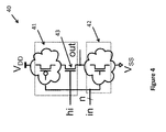
- the digital CMOS circuit arrangement according to the present disclosure may be used with digital CMOS circuits having multiple inputs for matching the electrical performance of the pull-down circuit with the pull-up circuit and vice versa, as shown in figure 4 .
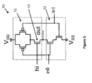
- a two-input CMOS AND logic gate 50 may be implemented as a skew resilient logic so as to compensate the effects of process variation by matching the electrical performance of the pull-down circuit 52 with the pull-up circuit 51.
- This may be achieved by providing at least one NMOS type performance matching transistor 53 between the PMOS transistors of the pull-up circuit 51 and the output node.
- the NMOS performance matching transistor 53 may be serially connected to the PMOS transistors of the pull-up circuit 51 and to the NMOS transistors of the pull-down circuit 52.
- the drain terminal of the at least one NMOS performance matching transistor 53 may be connected to the drain terminals of the PMOS transistors of the pull-up circuit 51, while the source terminal of the NMOS performance matching transistor 53 may be connected to the drain terminal of at least one of the NMOS transistor of the pull-down circuit 52.
- the NMOS performance matching transistor 53 in the pull-up path may cause the pull-up circuit 51 to experience the same process skew as the pull-down circuit 52, thereby causing the pull-up path to follow the same process variation trend, either slow or fast, as the pull-down path.
- the gate terminal of the NMOS performance matching transistor 53 may be connected to biasing means arranged for supplying a fixed voltage, e.g VDD, so that the performance matching transistor may be maintained in the on-state.
- the fixed voltage may be supplied directly from the power supply of the circuit, e.g VDD or VSS, thereby minimising the need for providing additional inputs for supplying the biasing voltage.
- the CMOS AND logic gate 50 may be implemented as a skew resilient logic so as to compensate the effects of process variation by matching the electrical performance of the pull-up circuit 51 with the pull-down circuit 52 by providing a performance matching transistor 33 of a P-type in the pull-down circuit 52 between the NMOS transistors and the output node.
- a Cascode Voltage Switch Logic (CVSL) 60 may be implemented as a skew resilient logic so as to compensate the effects of process variation by matching the electrical performance of the pull-down circuit 62 with the pull-up circuit 61.
- two NMOS performance matching transistors 63 may be provided in the pull-path, which may be serially connected to the PMOS transistors in the pull-up path.
- the two NMOS performance matching transistors 63 in the pull-up path will experience the same process skew as the NMOS transistors in the pull-down circuit 62 causing the pull-up path to follow the same process corner trend, slow-slow or fast-fast, as the pull-down path.
- each of the NMOS performance matching transistor 63 may be connected to biasing means arranged for supplying a fixed voltage, e.g VDD, so that the performance matching transistor may be maintained in the on-state.
- a fixed voltage e.g VDD
- the fixed voltage may be supplied directly from the power supply of the circuit, e.g VDD or VSS, thereby minimising the need for providing additional inputs for supplying the biasing voltage.
- the CSVL circuit 60 may be implemented as a skew resilient logic so as to compensate the effects of process variation by matching the electrical performance of the pull-up circuit 61 with the pull-down circuit 62 by providing performance matching transistors 63 of a P-type in the pull-down circuit 62, which may be serially connected to the NMOS transistors of the pull-down circuit 62.
- the present disclosure may be used for the development of skew resilient CMOS logic families, such as logic gates or other circuits, having lower area overhead and reduced propagation delay than comparable standard CMOS implementations.
- the biasing means may be provided with an inverter the output of which may be connected to the gate terminal of the performance matching transistor.
- the inverter may be used to control the switching activity of the matching performance transistor so as to improve the on to off current ratio of the corresponding pull-up and pull-down circuits.
- the inverter circuit may be used for power gating the digital CMOS circuit so as achieve a leakage power reduction, which may lead to the scaling of the operating voltage and/or process skew of the digital CMOS circuit due to the improved on to off ratio.
- a CMOS inverter 70 may be implemented as a skew resilient logic so as to compensate the effects of process variation by matching the electrical performance of the pull-down circuit 72 with the pull-up circuit 71.
- this may be achieved by providing a performance matching transistor 73 of an N-type in the pull-up circuit 71 between the PMOS transistor and the output node.
- the NMOS performance matching transistor 73 in the pull-up path may cause the pull-up circuit 71 to experience the same process skew as the pull-down circuit 72, thereby causing the pull-up path to follow the same process variation trend, either slow or fast, as the pull-down path.
- the gate terminal of the NMOS performance matching transistor 73 may be connected to the output of an inverter 74, which may be part of the biasing means, the input of which may connected to the gate terminal of at least one of the transistors in the pull-up 71 or pull-down circuit 72.
- the input of the inverter 74 is connected to the input node of the CMOS inverter 70, so that when the input voltage supplied to the input node of the CMOS inverter 70 switches from a high voltage, e.g VDD, to a low voltage, e.g Vss, causes the NMOS performance matching transistor 73 to switch from the off-state to the on-state, thereby causing the pull-up path to follow the same process corner trend with that of the pull-down path.
- a high voltage e.g VDD
- Vss a low voltage
- CMOS inverter 70 when the input voltage supplied to the input node of the CMOS inverter 70 switches from a low voltage, e.g Vss, to a high voltage, e.g VDD, causes the NMOS performance matching transistor 73 to switch from the on-state to the off-state, thereby reducing the leakage power of the CMOS inverter 70, which may lead to the scaling of the operating voltage and/or process skew due to the improved on to off current ratio.
- Vss low voltage
- VDD high voltage
- an inverter 84 may be used to control the switching activity of a PMOS performance matching transistor 83 provided in pull-down circuit 82 of a circuit device, such as CMOS inverter 80, implemented as a skew resilient logic so as to compensate the effects of process variation by matching the electrical performance of the pull-up circuit 81 with the pull-down circuit 82.
- the gate terminal of the PMOS performance matching transistor 83 may be connected to the output of an inverter 84, which may be part of the biasing means, the input of which may connected to the gate terminal of at least one of the transistors in the pull-up 81 or pull-down circuit 82.
- the input of the inverter 84 is connected to the input node of the CMOS inverter 80, so that when the input voltage supplied to the input node of the CMOS inverter 80 switches from a low voltage, e.g Vss, to a high voltage, e.g VDD, causes the PMOS performance matching transistor 83 to switch from the off-state to the on-state, thereby causing the pull-down path to follow the same process corner trend with that of the pull-up path.
- a low voltage e.g Vss
- VDD high voltage
- the input voltage supplied to the input node of the CMOS inverter 80 switches from a high voltage, e.g VDD, to a low voltage, e.g Vss, causes the PMOS performance matching transistor 83 to switch from the on-state to the off-state, thereby reducing the leakage power of the CMOS inverter 80, which may lead to the scaling of the operating voltage and/or process skew due to the improved on to off current ratio
- the use of the inverter circuit to control the switching activity of the performance matching transistor greatly reduces the sizing requirements of the transistors in the pull-up and pull-down circuits for achieving a predetermine device performance. This is due to the improved on to off current ratio, which may result in the size ratio between the transistors of the pull-up and pull-down circuit being smaller than comparable standard CMOS implementations. This is because, in this configuration the on and off-current of the pull-up and pull-down paths can be controlled by means of the inverter. Therefore, by controlling both the on and off-currents of the pull-up and pull-down paths the process of identifying the optimal width ratio for the transistors in the pull-down and pull-up path is greatly simplified.
- the size, e.g the transistor width and/or length, ratio between the transistors of the pull-up and pull-down circuits may be chosen such that a predetermined device performance may be achieved in combination with the presence of the performance matching transistor.
- a CMOS digital circuit 90 such as a CMOS inverter may be implemented as a skew resilient logic according to embodiments of the present invention, so as to compensate the effects of process variation by matching the electrical performance of the pull-up circuit 91 with the pull-down circuit 92, which may be achieved by providing a PMOS performance matching transistor 93 between the at least one NMOS transistor of the pull-down circuit 92 and the output node of the CMOS digital circuit 90.
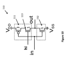
- CMOS digital circuit 110 such as a CMOS inverter
- CMOS inverter may be implemented as a skew resilient logic according to embodiments of the present invention, so as to compensate the effects of process variation by matching the electrical performance of the pull-down circuit 112 with the pull-up circuit 111 by providing a NMOS performance matching transistor 113 between the PMOS transistors of the pull-up circuit 111 and the output node of the CMOS digital circuit 110.
- the size of the PMOS transistors of the digital CMOS circuit 110 may be at most three times the size selected for the NMOS transistors of the digital CMOS circuit 110.
- digital CMOS circuits may be implemented with transistors that have no explicit bulk terminal connections.
- the transistors in the pull-up and pull-down circuits and the at least one performance matching transistor may be multi-gate transistors such as finFET, tunnel field-effect transistors, or the like.
Landscapes
- Engineering & Computer Science (AREA)
- Physics & Mathematics (AREA)
- Nonlinear Science (AREA)
- Computer Hardware Design (AREA)
- General Engineering & Computer Science (AREA)
- Theoretical Computer Science (AREA)
- Computing Systems (AREA)
- Mathematical Physics (AREA)
- General Physics & Mathematics (AREA)
- Power Engineering (AREA)
- Logic Circuits (AREA)
- Metal-Oxide And Bipolar Metal-Oxide Semiconductor Integrated Circuits (AREA)
Abstract
Description
- The present disclosure relates to digital CMOS circuits and more specifically to a process skew resilient digital CMOS circuit arrangement by which performance mismatch can be compensated.
- Advanced semiconductor fabrication techniques have resulted in the fabrication of devices, such as transistors, with continually decreasing feature sizes having a substantial amount of so called process variations. These process variations are due to the inability of accurately printing geometrical features and the inability to correctly control the diffusion of dopants. The presence of process variations translates to variations in key electrical parameters of the devices, which in turn leads to variations in the electrical performance of the fabricated devices. Process variations of the fabricated devices may be analysed using the process corners technique, which represent the extremes of these parameter variations within which the fabricated device must function correctly. The process variations using the process corners analysis technique may be differentiated between so called straight corners and skewed corners. Using the example of a CMOS circuit device designed using NMOS and PMOS transistors, the straight corners refer to process variations where both NMOS and PMOS transistors experience similar changes in device performance, e.g slow-slow, fast-fast, typical-typical. On the other hand, using the same example, in the skewed corners the NMOS and PMOS transistors experience opposite changes in device performance, e.g slow-fast, fast-slow, etc. A CMOS circuit device operating in skewed corners may lead to imbalanced timing paths and reduced operating noise margins, which may lead to inefficient implementations and ultimately limit the voltage scaling potential. For example, an inverter CMOS circuit operating in skewed corners may experience a delay mismatch between the rising and falling transitions of the inverter output due to the performance mismatch between the NMOS and PMOS transistors.
- Current CMOS design techniques compensate the effects of process variations in CMOS circuit devices operating in skewed corners using a biasing technique whereby the bulk terminal connection of the transistor is biased to a predetermined voltage level so as to adjust the performance of the NMOS and PMOS devices. However, such solution substantially increases the power consumption requirements of the CMOS devices, which is an undesirable effect in the design of low-power digital circuits. Moreover, new CMOS devices, such as finFET or tunnel FET devices, do not feature an explicit bulk terminal thus their performance cannot be adjusted using the biasing technique.
- In the absence of a bulk terminal connection the effects of process variation in CMOS devices operating in skewed corners may be compensated by increasing the size of the transistors. For example, in a 90nm CMOS process technology a PMOS/NMOS width ratio of 11 may be necessary for achieving best noise margin at low-voltage. However, increasing the size of the transistors results in a substantial increase of the area overhead and power consumption of the digital circuit, which is undesirable for the design of high density and low power digital circuits.
- It is an aim of the present disclosure to provide a digital CMOS circuit arrangement in which the effects of process variation in digital CMOS circuits operating in skewed corners may be compensated in an alternative way.
- This aim is achieved according to the disclosure with the digital CMOS circuit arrangement showing the technical characteristics of the first independent claim.
- More in particular according to embodiments of the present disclosure a digital CMOS circuit arrangement is provided. The digital CMOS circuit arrangement is provided with at least one pull-up circuit, which comprises at least one transistor of a first type. The first type transistor is operable between an on-state and an off-state based on a predetermined voltage level supplied to a gate terminal of the at least one first type transistor. The pull-up circuit is arranged when the at least one first type transistor is in the on-state to switch an output node of the digital CMOS circuit arrangement from a first voltage level to a second voltage level within a rising transition delay. The digital CMOS circuit arrangement is further provided with at least one pull-down circuit, which comprises at least one transistor of a second type. The second type transistor is operable between an on-state and an off-state based on a predetermined voltage level supplied to a gate terminal of the at least one second type transistor. The pull-down circuit is arranged when the at least one second type transistor is in the on-state to switch the voltage level of the output node of the digital CMOS circuit arrangement from the second voltage level to the first voltage level within a falling transition delay, which is different from the rising transition delay of the pull-up circuit. The delay difference between the rising and falling transition indicating a performance mismatch between the first and second type transistors. The performance mismatch may be due to the effects of process variation, which would cause the digital CMOS circuit arrangement to operate in skewed corners. The first and second type transistors is serially connected at the output node of the digital circuit. For example, the drain terminal of the first type transistor may be connected to the drain terminal of the second type transistor. The digital CMOS circuit arrangement may comprise at least one performance matching transistor, which may be serially connected to the first and second type transistors. For example, the performance matching transistor may be provided between the first type and second type transistors. The gate terminal of the at least one matching performance transistor may be connected to biasing means arranged for biasing the at least one performance matching transistor in such a way so as to compensate the performance mismatch between the at least one first and second type transistors.
- It has been found that the use of a performance matching transistor can overcome or reduce the need for compensating the effects of process variation by means of biasing or transistor sizing and provide an alternative way to, ensure reliable device operation for digital CMOS devices operating in skewed process corners. The introduction of the performance matching transistor in the digital CMOS circuit arrangement may ensure that the pull-up and pull-down circuits experience the same process skew. Therefore, connecting the performance matching transistor in series with the first and second type transistors may ensure that the pull-up path follows the same process variation trend, either slow or fast, as the pull-down path. As a result, the introduction of the performance matching transistor can cause the digital CMOS device to operate in the straight corners instead of the skewed corners so that the first type and second type transistors experience similar changes in device performance, e.g slow-slow, fast-fast, etc, which may lead to the development of process skew resilient logic families.
- According to embodiments of the present disclosure, the biasing means may be arranged for supplying a predetermined fixed voltage to the gate terminal of the performance matching transistor so that the performance matching transistor is maintained in the on-state. This may have as a result that the operation of the digital CMOS circuit may be better controlled since in this configuration the on-current for the pull-up and pull-down paths are determined by the performance matching transistor rather than the transistors of the pull-up and pull-down circuits. Furthermore, the fixed voltage may be supplied directly from the power supply of the circuit, e.g VDD or VSS, thereby minimising the need for providing additional inputs for supplying the biasing voltage. Moreover, in the case where an additional input is provided, the fixed voltage may be regulated so as to ensure better compensation of the process variation effects. For example, this may be achieved by providing a control voltage to the performance matching transistor, which may be adapted based on the parametric variations determined by the manufacturing process, supply voltage variations, or temperature.
- According to embodiments of the present disclosure, the biasing means may comprise an inverter circuit the output of which is connected to the gate terminal of at least one performance matching transistor. The use of an inverter to control the switching activity of the matching performance transistor may improve the on to off current ratio of the corresponding pull-up and pull-down circuits. As a result, the use of the inverter may greatly simplify the process of identifying the optimal width ratio between the different transistors of the digital CMOS circuit. This is because, in this configuration the on and off-currents of the pull-up and pull-down paths can be controlled by means of the inverter. As a result, a better on-to-off current ratio can be achieved between the pull-up and pull-down network by controlling both transitions between on and off states. Therefore, by controlling both the on and off-currents of the pull-up and pull-down paths the process of identifying the optimal width ratio for the transistors in the pull-down and pull-up path is greatly simplified.
- According to embodiments of the present invention, the size, e.g the transistor width and/or length, ratio between the first and second type transistors may be chosen such that a predetermined device performance is achieved in combination with the presence of the presence of the performance matching transistor. For example, the width of the first type transistor may be at least equal to the size of the second type transistor, which ensures low area overhead of the digital CMOS circuit. The size of the first type transistor may be at most three time the size of the second type transistor so as to ensure faster device performance. This size relationship between the first and second type transistors is achievable due to the presence of the performance matching transistor.
- The disclosure will be further elucidated by means of the following description and the appended figures.
-
Figures 1 shows an example of a digital CMOS circuit according to prior art. -
Figures 2 to 8 show examples of digital CMOS circuits according to embodiments of the present disclosure -
Figures 9 and10 show examples of sizing ratios between pull-up and pull-down transistors according to embodiments of the present invention. - The present disclosure will be described with respect to particular embodiments and with reference to certain drawings but the disclosure is not limited thereto but only by the claims. The drawings described are only schematic and are non-limiting. In the drawings, the size of some of the elements may be exaggerated and not drawn on scale for illustrative purposes. The dimensions and the relative dimensions do not necessarily correspond to actual reductions to practice of the disclosure.
- Furthermore, the terms first, second, third and the like in the description and in the claims, are used for distinguishing between similar elements and not necessarily for describing a sequential or chronological order. The terms are interchangeable under appropriate circumstances and the embodiments of the disclosure can operate in other sequences than described or illustrated herein.
- Moreover, the terms top, bottom, over, under and the like in the description and the claims are used for descriptive purposes and not necessarily for describing relative positions. The terms so used are interchangeable under appropriate circumstances and the embodiments of the disclosure described herein can operate in other orientations than described or illustrated herein.
- Furthermore, the various embodiments, although referred to as "preferred" are to be construed as exemplary manners in which the disclosure may be implemented rather than as limiting the scope of the disclosure.
- The term "comprising", used in the claims, should not be interpreted as being restricted to the elements or steps listed thereafter; it does not exclude other elements or steps. It needs to be interpreted as specifying the presence of the stated features, integers, steps or components as referred to, but does not preclude the presence or addition of one or more other features, integers, steps or components, or groups thereof. Thus, the scope of the expression "a device comprising A and B" should not be limited to devices consisting only of components A and B, rather with respect to the present disclosure, the only enumerated components of the device are A and B, and further the claim should be interpreted as including equivalents of those components.
- As used herein, with "transistor size" it is intended to mean the area occupied by the transistor designed in a specific process technology. The size of the transistor is defined by its dimensions, e.g width, length, or height, which can be adapted to meet a predetermine electrical performance.
- As used herein, with "size ratio" it is intended to mean the transistor size comparison between NMOS and PMOS transistors of a digital CMOS circuits.
- Embodiments of the present disclosure may be exemplified with the aid of the exemplified digital CMOS circuits shown in
figures 1 to 10 . -
Figure 1 show an example of a prior art digitalCMOS circuit device 10 comprising a pull-upcircuit 11 and a pull-down circuit 12 each respectively comprising at least one first type transistor, e.g PMOS, and at least one second type transistor, e.g NMOS transistor, the gate terminals of which are connected to a common input node. The pull-up 11 and pull-down 12 circuits are operable between an on-state and an off-state depending on the voltage level supplied to the gate terminal of the corresponding first and second type transistors. For example, in the case of a CMOS inverter the pull-upcircuit 11 may be activated by supplying in the gate terminal of the PMOS transistor a first voltage level, e.g a low voltage equal to the VSS voltage, while the pull-down 12 network may be activated by supplying to the gate terminal of the NMOS transistor a second voltage level, e.g a high voltage level equal to the VDD voltage. Depending on which one of the pull-up 11 or pull-down 12 circuits is activated the voltage at the output node will switch to the corresponding voltage level within a predetermined transition delay. For example, in the case where a low voltage level is supplied to the input node, the pull-upcircuit 11 will be activated causing the voltage at the output node to switch from a low voltage level to a high voltage level within a rising transition delay Tr. In the case where the pull-down circuit 12 is activated instead, the output voltage at the output node will switch from a high voltage level to a low voltage level within a falling transition delay Tf. In a CMOS digital circuit operating in straight process corners, e.g slow-slow, fast-fast, etc, the rising Tr and falling Tf transition delays may be substantially equal since the transistors in the pull-up 11 and pull-down 12 circuits experience same changes in the electrical performance. However, in the case where theCMOS circuit 10 operates in the skewed process corners the rising Tr and falling Tf transition delays may not be equal due to the electrical performance mismatch between the transistors in the pull-up 11 and pull-down 12 circuits, as shown infigure 1 . A CMOS circuit device operating in skewed corners may lead to imbalanced timing paths and reduced operating noise margins, which may lead to inefficient implementations and ultimately limit the voltage scaling potential. - To compensate the effects of process variation in digital CMOS circuits operating in skewed corners the CMOS circuit arrangement of the present disclosure may be used. According to embodiments of the present disclosure a performance matching transistor may be serially connected to the at least one first type transistor, e.g PMOS, of the pull-up circuit and the at least one second type transistor, e.g NMOS, of the pull-down circuit. The gate terminal of the performance matching transistor may be connected to biasing means arranged for biasing the at least one performance matching transistor in such a way so as to compensate the performance mismatch between the at least one first and second type transistors. As a result, with the digital CMOS circuit arrangement of the present invention the process variation effects of a CMOS circuit operating in skewed corners may be compensated without the need for explicit bulk terminal connection or by substantially increasing the size, e.g width and/or length, of the transistors in the pull-up and pull-down circuits.
-
Figure 2 shows an example of adigital CMOS circuit 20 according to embodiments of the present disclosure. In this case aCMOS inverter 20 operating in a similar manner to the CMOS inverter offigure 1 may be used as an example. TheCMOS inverter 20 may be implemented as a skew resilient logic so as to compensate the effects of process variation by matching the electrical performance of the pull-down circuit 22 with the pull-upcircuit 21. This may be achieved by providing aperformance matching transistor 23 of an N-type in the pull-upcircuit 21 between the PMOS transistor and the output node of theCMOS inverter 20. The NMOSperformance matching transistor 23 in the pull-up path may cause the pull-upcircuit 21 to experience the same process skew as the pull-down circuit 22, thereby causing the pull-up path to follow the same process variation trend, either slow or fast, as the pull-down path. The gate terminal of the NMOSperformance matching transistor 23 may be connected to biasing means arranged for supplying a fixed voltage, e.g VDD, so that the performance matching transistor may be maintained in the on-state. For example, the fixed voltage may be supplied directly from the power supply of the circuit, e.g VDD or VSS, thereby minimising the need for providing additional inputs for supplying the biasing voltage. - According to embodiments of the present disclosure, in order to match the electrical performance of the pull-up circuit with the pull-down circuit, a PMOS performance matching transistor may be provided in the pull-down circuit of a digital CMOS device.
Figure 3 shows a digital CMOS device, such as aCMOS inverter 30 operating in a similar manner to the one presented infigure 2 . TheCMOS inverter 30 may be implemented as a skew resilient logic so as to compensate the effects of process variation by matching the electrical performance of the pull-upcircuit 31 with the pull-down circuit 32. This may be achieved by providing aperformance matching transistor 33 of a P-type in the pull-down circuit 32 between the NMOS transistor and the output node. The PMOSperformance matching transistor 33 in the pull-down path may cause the pull-down circuit 32 to experience the same process skew as the pull-upcircuit 31, thereby causing the pull-down path to follow the same process variation trend, either slow or fast, as the pull-up path. The gate terminal of the PMOSperformance matching transistor 33 may be connected to biasing means arranged for supplying a fixed voltage, e.g Vss, so that theperformance matching transistor 33 may be maintained in the on-state. For example, the fixed voltage may be supplied directly from the power supply of the circuit, e.g VDD or VSS, thereby minimising the need for providing additional inputs for supplying the biasing voltage. - According to embodiments of the present invention, the digital CMOS circuit arrangement according to the present disclosure may be used with digital CMOS circuits having multiple inputs for matching the electrical performance of the pull-down circuit with the pull-up circuit and vice versa, as shown in
figure 4 . - For example, as shown in
figure 5 , a two-input CMOS ANDlogic gate 50 may be implemented as a skew resilient logic so as to compensate the effects of process variation by matching the electrical performance of the pull-down circuit 52 with the pull-upcircuit 51. This may be achieved by providing at least one NMOS typeperformance matching transistor 53 between the PMOS transistors of the pull-upcircuit 51 and the output node. For example, the NMOSperformance matching transistor 53 may be serially connected to the PMOS transistors of the pull-upcircuit 51 and to the NMOS transistors of the pull-down circuit 52. In the exemplified circuit arrangement shown infigure 5 , the drain terminal of the at least one NMOSperformance matching transistor 53 may be connected to the drain terminals of the PMOS transistors of the pull-upcircuit 51, while the source terminal of the NMOSperformance matching transistor 53 may be connected to the drain terminal of at least one of the NMOS transistor of the pull-down circuit 52. The NMOSperformance matching transistor 53 in the pull-up path may cause the pull-upcircuit 51 to experience the same process skew as the pull-down circuit 52, thereby causing the pull-up path to follow the same process variation trend, either slow or fast, as the pull-down path. The gate terminal of the NMOSperformance matching transistor 53 may be connected to biasing means arranged for supplying a fixed voltage, e.g VDD, so that the performance matching transistor may be maintained in the on-state. For example, the fixed voltage may be supplied directly from the power supply of the circuit, e.g VDD or VSS, thereby minimising the need for providing additional inputs for supplying the biasing voltage. It should be noted, that similarly to previous embodiments the CMOS ANDlogic gate 50 may be implemented as a skew resilient logic so as to compensate the effects of process variation by matching the electrical performance of the pull-upcircuit 51 with the pull-down circuit 52 by providing aperformance matching transistor 33 of a P-type in the pull-down circuit 52 between the NMOS transistors and the output node. - According to embodiments of the present invention, a Cascode Voltage Switch Logic (CVSL) 60 may be implemented as a skew resilient logic so as to compensate the effects of process variation by matching the electrical performance of the pull-
down circuit 62 with the pull-upcircuit 61. In this case, two NMOSperformance matching transistors 63 may be provided in the pull-path, which may be serially connected to the PMOS transistors in the pull-up path. In this configuration, the two NMOSperformance matching transistors 63 in the pull-up path will experience the same process skew as the NMOS transistors in the pull-down circuit 62 causing the pull-up path to follow the same process corner trend, slow-slow or fast-fast, as the pull-down path. The gate terminal of each of the NMOSperformance matching transistor 63 may be connected to biasing means arranged for supplying a fixed voltage, e.g VDD, so that the performance matching transistor may be maintained in the on-state. For example, the fixed voltage may be supplied directly from the power supply of the circuit, e.g VDD or VSS, thereby minimising the need for providing additional inputs for supplying the biasing voltage. It should be noted, that similarly to previous embodiments theCSVL circuit 60 may be implemented as a skew resilient logic so as to compensate the effects of process variation by matching the electrical performance of the pull-upcircuit 61 with the pull-down circuit 62 by providingperformance matching transistors 63 of a P-type in the pull-down circuit 62, which may be serially connected to the NMOS transistors of the pull-down circuit 62. - According to embodiments of the present disclosure, the present disclosure may be used for the development of skew resilient CMOS logic families, such as logic gates or other circuits, having lower area overhead and reduced propagation delay than comparable standard CMOS implementations.
- According to embodiments of the present disclosure, the biasing means may be provided with an inverter the output of which may be connected to the gate terminal of the performance matching transistor. The inverter may be used to control the switching activity of the matching performance transistor so as to improve the on to off current ratio of the corresponding pull-up and pull-down circuits. For example, the inverter circuit may be used for power gating the digital CMOS circuit so as achieve a leakage power reduction, which may lead to the scaling of the operating voltage and/or process skew of the digital CMOS circuit due to the improved on to off ratio.
- For example, as shown in
figure 7 , aCMOS inverter 70 may be implemented as a skew resilient logic so as to compensate the effects of process variation by matching the electrical performance of the pull-down circuit 72 with the pull-upcircuit 71. As previously discussed, this may be achieved by providing aperformance matching transistor 73 of an N-type in the pull-upcircuit 71 between the PMOS transistor and the output node. The NMOSperformance matching transistor 73 in the pull-up path may cause the pull-upcircuit 71 to experience the same process skew as the pull-down circuit 72, thereby causing the pull-up path to follow the same process variation trend, either slow or fast, as the pull-down path. The gate terminal of the NMOSperformance matching transistor 73 may be connected to the output of aninverter 74, which may be part of the biasing means, the input of which may connected to the gate terminal of at least one of the transistors in the pull-up 71 or pull-down circuit 72. For example, as shown infigure 7 , the input of theinverter 74 is connected to the input node of theCMOS inverter 70, so that when the input voltage supplied to the input node of theCMOS inverter 70 switches from a high voltage, e.g VDD, to a low voltage, e.g Vss, causes the NMOSperformance matching transistor 73 to switch from the off-state to the on-state, thereby causing the pull-up path to follow the same process corner trend with that of the pull-down path. In contrast, when the input voltage supplied to the input node of theCMOS inverter 70 switches from a low voltage, e.g Vss, to a high voltage, e.g VDD, causes the NMOSperformance matching transistor 73 to switch from the on-state to the off-state, thereby reducing the leakage power of theCMOS inverter 70, which may lead to the scaling of the operating voltage and/or process skew due to the improved on to off current ratio. - Similarly, as shown in
figure 8 , aninverter 84 may be used to control the switching activity of a PMOSperformance matching transistor 83 provided in pull-down circuit 82 of a circuit device, such asCMOS inverter 80, implemented as a skew resilient logic so as to compensate the effects of process variation by matching the electrical performance of the pull-upcircuit 81 with the pull-down circuit 82. In this case, the gate terminal of the PMOSperformance matching transistor 83 may be connected to the output of aninverter 84, which may be part of the biasing means, the input of which may connected to the gate terminal of at least one of the transistors in the pull-up 81 or pull-down circuit 82. For example, as shown infigure 8 , the input of theinverter 84 is connected to the input node of theCMOS inverter 80, so that when the input voltage supplied to the input node of theCMOS inverter 80 switches from a low voltage, e.g Vss, to a high voltage, e.g VDD, causes the PMOSperformance matching transistor 83 to switch from the off-state to the on-state, thereby causing the pull-down path to follow the same process corner trend with that of the pull-up path. In contrast, when the input voltage supplied to the input node of theCMOS inverter 80 switches from a high voltage, e.g VDD, to a low voltage, e.g Vss, causes the PMOSperformance matching transistor 83 to switch from the on-state to the off-state, thereby reducing the leakage power of theCMOS inverter 80, which may lead to the scaling of the operating voltage and/or process skew due to the improved on to off current ratio - According to embodiments of the present disclosure, the use of the inverter circuit to control the switching activity of the performance matching transistor greatly reduces the sizing requirements of the transistors in the pull-up and pull-down circuits for achieving a predetermine device performance. This is due to the improved on to off current ratio, which may result in the size ratio between the transistors of the pull-up and pull-down circuit being smaller than comparable standard CMOS implementations. This is because, in this configuration the on and off-current of the pull-up and pull-down paths can be controlled by means of the inverter. Therefore, by controlling both the on and off-currents of the pull-up and pull-down paths the process of identifying the optimal width ratio for the transistors in the pull-down and pull-up path is greatly simplified. For example, the size, e.g the transistor width and/or length, ratio between the transistors of the pull-up and pull-down circuits may be chosen such that a predetermined device performance may be achieved in combination with the presence of the performance matching transistor. For example, as shown in
Figure 9 , a CMOSdigital circuit 90, such as a CMOS inverter may be implemented as a skew resilient logic according to embodiments of the present invention, so as to compensate the effects of process variation by matching the electrical performance of the pull-upcircuit 91 with the pull-down circuit 92, which may be achieved by providing a PMOSperformance matching transistor 93 between the at least one NMOS transistor of the pull-down circuit 92 and the output node of the CMOSdigital circuit 90. In this case, the transistor sizes for the NMOS and PMOS transistors in digital CMOS circuit may be selected to be equal. In a further example, as shown inFigure 10 , a CMOSdigital circuit 110, such as a CMOS inverter, may be implemented as a skew resilient logic according to embodiments of the present invention, so as to compensate the effects of process variation by matching the electrical performance of the pull-down circuit 112 with the pull-upcircuit 111 by providing a NMOSperformance matching transistor 113 between the PMOS transistors of the pull-upcircuit 111 and the output node of the CMOSdigital circuit 110. In this case, the size of the PMOS transistors of thedigital CMOS circuit 110 may be at most three times the size selected for the NMOS transistors of thedigital CMOS circuit 110. - According to embodiments of the present disclosure, digital CMOS circuits may be implemented with transistors that have no explicit bulk terminal connections. For example, the transistors in the pull-up and pull-down circuits and the at least one performance matching transistor may be multi-gate transistors such as finFET, tunnel field-effect transistors, or the like.
Claims (13)
- A digital CMOS circuit (20, 30, 40, 50, 60, 70, 80, 90, 110) comprising:at least one pull-up circuit (21, 31, 41, 51, 61, 71, 81, 91, 111) comprising at least one transistor of a first type, which is operable between an on-state and an off-state based on a predetermined voltage level supplied to a gate terminal of the at least one first type transistor, wherein the pull-up circuit (21, 31, 41, 51, 61, 71, 81, 91, 111) is arranged when the at least one first type transistor is in the on-state to switch an output node of the digital CMOS circuit (20, 30, 40, 50, 60, 70, 80, 90, 110) from a first voltage level to a second voltage level within a rising transition delay;at least one pull-down circuit (22, 32, 42, 52, 62, 72, 82, 92, 112) comprising at least one transistor of a second type, which is operable between an on-state and an off-state based on a predetermined voltage level supplied to a gate terminal of the at least one second type transistor, wherein the pull-down circuit (22, 32, 42, 52, 62, 72, 82, 92, 112) is arranged when the at least one second type transistor is in the on-state to switch the voltage level of the output node of the digital CMOS circuit (20, 30, 40, 50, 60, 70, 80, 90, 110) from the second voltage level to the first voltage level within a falling transition delay, which is different from the rising transition delay of the pull-up circuit (20, 30, 40, 50, 60, 70, 80, 90, 110) indicating a performance mismatch between the first and second type transistors; andwherein the first and second type transistors are serially connected at the output node of the digital circuit;characterised in that the digital CMOS circuit (20, 30, 40, 50, 60, 70, 80, 90, 110) comprises at least one performance matching transistor (23, 33, 43, 53, 63, 73, 83, 93, 113) serially connected to the first and second type transistors, the gate terminal of which is connected to biasing means arranged for biasing the at least one performance matching transistor (23, 33, 43, 53, 63, 73, 83, 93, 113) in such a way so as to compensate the performance mismatch between the at least one first and second type transistors.
- The digital CMOS circuit (20, 30, 40, 50, 60, 70, 80, 90, 110) of claim 1, wherein the biasing means is arranged for supplying a fixed voltage to the gate terminal of the performance matching transistor (23, 33, 43, 53, 63, 73, 83, 93, 113) so as to maintain the performance matching transistor (23, 33, 43, 53, 63, 73, 83, 93, 113) in the on-state.
- The digital CMOS circuit (20, 30, 40, 50, 60, 70, 80, 90, 110) of claim 1 or 2, wherein the biasing means comprises an inverter circuit (74, 84) the output of which is connected to the gate terminal of at least one performance matching transistor (74, 84) and its input is connected to at least one of the gate terminals of the first and second type transistors.
- The digital CMOS circuit (20, 30, 40, 50, 60, 70, 80, 90, 110) of any one of claims 1 to 3, wherein the size ratio between the first and second type transistors is chosen such that a predetermined device performance is achieved.
- The digital CMOS circuit (20, 30, 40, 50, 60, 70, 80, 90, 110) of any one of the preceding claims, wherein the size of the first type transistor is at least equal to the size of the second type transistor.
- The digital CMOS circuit (20, 30, 40, 50, 60, 70, 80, 90, 110) of any one claims 1 to 4, wherein the size of the first type transistor is at most three time the size of the second type transistor.
- The digital CMOS circuit (20, 30, 40, 50, 60, 70, 80, 90, 110) of any one of the preceding claims, wherein the first type transistor is an N-type transistor and the second type transistor is a P-type transistor.
- The digital CMOS circuit (20, 30, 40, 50, 60, 70, 80, 90, 110) of any one of the preceding claims, wherein the at least one performance matching transistor is provided between the first type transistor and the output node of the digital CMOS circuit.
- The digital CMOS circuit (20, 30, 40, 50, 60, 70, 80, 90, 110) of claim 8, wherein the at least one performance matching transistor is an N-type transistor.
- The digital CMOS circuit (20, 30, 40, 50, 60, 70, 80, 90, 110) of any one of claims 1 to 7, wherein the at least one performance matching transistor is provided between the second type transistor and the output node of the digital CMOS circuit (20, 30, 40, 50, 60, 70, 80, 90, 110).
- The digital CMOS circuit (20, 30, 40, 50, 60, 70, 80, 90, 110) of claim 10, wherein the at least one performance transistor is a P-type transistor.
- The digital CMOS circuit (20, 30, 40, 50, 60, 70, 80, 90, 110) of any one of the preceding claims, wherein the first type transistor, the second type transistor, and the at least one performance matching transistor (23, 33, 43, 53, 63, 73, 83, 93, 113) are transistors with no bulk terminal such as multi-gate transistors or tunnel field-effect transistors (TFET).
- A digital system comprising a digital CMOS circuit (20, 30, 40, 50, 60, 70, 80, 90, 110) according to claims 1 to 12.
Priority Applications (2)
| Application Number | Priority Date | Filing Date | Title |
|---|---|---|---|
| EP14196607.7A EP3029831B1 (en) | 2014-12-05 | 2014-12-05 | Process skew resilient digital CMOS circuit |
| US14/959,518 US20160161979A1 (en) | 2014-12-05 | 2015-12-04 | Process Skew Resilient Digital CMOS Circuit |
Applications Claiming Priority (1)
| Application Number | Priority Date | Filing Date | Title |
|---|---|---|---|
| EP14196607.7A EP3029831B1 (en) | 2014-12-05 | 2014-12-05 | Process skew resilient digital CMOS circuit |
Publications (2)
| Publication Number | Publication Date |
|---|---|
| EP3029831A1 true EP3029831A1 (en) | 2016-06-08 |
| EP3029831B1 EP3029831B1 (en) | 2018-07-25 |
Family
ID=52011068
Family Applications (1)
| Application Number | Title | Priority Date | Filing Date |
|---|---|---|---|
| EP14196607.7A Not-in-force EP3029831B1 (en) | 2014-12-05 | 2014-12-05 | Process skew resilient digital CMOS circuit |
Country Status (2)
| Country | Link |
|---|---|
| US (1) | US20160161979A1 (en) |
| EP (1) | EP3029831B1 (en) |
Citations (3)
| Publication number | Priority date | Publication date | Assignee | Title |
|---|---|---|---|---|
| US6670836B1 (en) * | 2002-08-15 | 2003-12-30 | Micron Technology, Inc. | Differential buffer having bias current gated by associated signal |
| US8004330B1 (en) * | 2009-11-30 | 2011-08-23 | Pmc-Sierra, Inc. | Reduction of electromagnetic interference for differential signals |
| US20120250734A1 (en) * | 2011-03-31 | 2012-10-04 | Hynix Semiconductor Inc. | Data output circuit of semiconductor apparatus |
Family Cites Families (1)
| Publication number | Priority date | Publication date | Assignee | Title |
|---|---|---|---|---|
| US6278295B1 (en) * | 1998-02-10 | 2001-08-21 | Cypress Semiconductor Corp. | Buffer with stable trip point |
-
2014
- 2014-12-05 EP EP14196607.7A patent/EP3029831B1/en not_active Not-in-force
-
2015
- 2015-12-04 US US14/959,518 patent/US20160161979A1/en not_active Abandoned
Patent Citations (3)
| Publication number | Priority date | Publication date | Assignee | Title |
|---|---|---|---|---|
| US6670836B1 (en) * | 2002-08-15 | 2003-12-30 | Micron Technology, Inc. | Differential buffer having bias current gated by associated signal |
| US8004330B1 (en) * | 2009-11-30 | 2011-08-23 | Pmc-Sierra, Inc. | Reduction of electromagnetic interference for differential signals |
| US20120250734A1 (en) * | 2011-03-31 | 2012-10-04 | Hynix Semiconductor Inc. | Data output circuit of semiconductor apparatus |
Also Published As
| Publication number | Publication date |
|---|---|
| EP3029831B1 (en) | 2018-07-25 |
| US20160161979A1 (en) | 2016-06-09 |
Similar Documents
| Publication | Publication Date | Title |
|---|---|---|
| US7292061B2 (en) | Semiconductor integrated circuit having current leakage reduction scheme | |
| US10133550B2 (en) | Ternary digit logic circuit | |
| US9543931B2 (en) | Low-voltage to high-voltage level shifter circuit | |
| US11942942B1 (en) | High-speed level-shifter for power-conversion applications | |
| US20150042393A1 (en) | Level shifter | |
| EP3070848A1 (en) | Nand gate circuit, display back panel, display and electronic device | |
| US20190341919A1 (en) | Boosted high-speed level shifter | |
| US10848154B2 (en) | Level shifter and driver circuit including the level shifter | |
| US9628081B2 (en) | Interconnect circuits having low threshold voltage P-channel transistors for a programmable integrated circuit | |
| KR20050084430A (en) | N-channel pull-up element and logic circuit | |
| CN115376450A (en) | Drive circuit, control method thereof and display panel | |
| KR20160137974A (en) | Multiplexor logic functions implemented with circuits having tunneling field effect transistors(tfets) | |
| US5502405A (en) | Method and apparatus for CML/EC to CMOS/TTL translators | |
| JPH02162824A (en) | Semiconductor integrated circuit device | |
| CN107623518B (en) | Level shifter circuit and method for applying level shifter circuit | |
| EP3029831B1 (en) | Process skew resilient digital CMOS circuit | |
| KR101738778B1 (en) | Post driver | |
| US20060081936A1 (en) | Semiconductor device for low power operation | |
| CN112689959A (en) | Transmission gate circuit, matrix switch and electronic equipment | |
| CN109144158B (en) | Quiescent current supply circuit for integrated circuit chip | |
| CN116406495A (en) | High-Speed Level Shifters for Power Conversion Applications | |
| US20170250688A1 (en) | Circuit and Method of a Level Shift Network with Increased Flexibility | |
| US7170772B1 (en) | Apparatus and method for dynamic control of double gate devices | |
| Lee et al. | On-chip interconnect boosting technique by using of 10-nm double gate-all-around (DGAA) transistor | |
| Patel et al. | Leakage current reduction techniques for CMOS circuits |
Legal Events
| Date | Code | Title | Description |
|---|---|---|---|
| PUAI | Public reference made under article 153(3) epc to a published international application that has entered the european phase |
Free format text: ORIGINAL CODE: 0009012 |
|
| AK | Designated contracting states |
Kind code of ref document: A1 Designated state(s): AL AT BE BG CH CY CZ DE DK EE ES FI FR GB GR HR HU IE IS IT LI LT LU LV MC MK MT NL NO PL PT RO RS SE SI SK SM TR |
|
| AX | Request for extension of the european patent |
Extension state: BA ME |
|
| STAA | Information on the status of an ep patent application or granted ep patent |
Free format text: STATUS: REQUEST FOR EXAMINATION WAS MADE |
|
| 17P | Request for examination filed |
Effective date: 20161124 |
|
| RBV | Designated contracting states (corrected) |
Designated state(s): AL AT BE BG CH CY CZ DE DK EE ES FI FR GB GR HR HU IE IS IT LI LT LU LV MC MK MT NL NO PL PT RO RS SE SI SK SM TR |
|
| RIC1 | Information provided on ipc code assigned before grant |
Ipc: H03K 5/08 20060101AFI20170727BHEP Ipc: G11C 29/02 20060101ALI20170727BHEP Ipc: H03K 19/0185 20060101ALI20170727BHEP |
|
| GRAP | Despatch of communication of intention to grant a patent |
Free format text: ORIGINAL CODE: EPIDOSNIGR1 |
|
| STAA | Information on the status of an ep patent application or granted ep patent |
Free format text: STATUS: GRANT OF PATENT IS INTENDED |
|
| INTG | Intention to grant announced |
Effective date: 20171010 |
|
| GRAJ | Information related to disapproval of communication of intention to grant by the applicant or resumption of examination proceedings by the epo deleted |
Free format text: ORIGINAL CODE: EPIDOSDIGR1 |
|
| STAA | Information on the status of an ep patent application or granted ep patent |
Free format text: STATUS: REQUEST FOR EXAMINATION WAS MADE |
|
| INTC | Intention to grant announced (deleted) | ||
| GRAP | Despatch of communication of intention to grant a patent |
Free format text: ORIGINAL CODE: EPIDOSNIGR1 |
|
| STAA | Information on the status of an ep patent application or granted ep patent |
Free format text: STATUS: GRANT OF PATENT IS INTENDED |
|
| INTG | Intention to grant announced |
Effective date: 20180312 |
|
| GRAS | Grant fee paid |
Free format text: ORIGINAL CODE: EPIDOSNIGR3 |
|
| GRAA | (expected) grant |
Free format text: ORIGINAL CODE: 0009210 |
|
| STAA | Information on the status of an ep patent application or granted ep patent |
Free format text: STATUS: THE PATENT HAS BEEN GRANTED |
|
| AK | Designated contracting states |
Kind code of ref document: B1 Designated state(s): AL AT BE BG CH CY CZ DE DK EE ES FI FR GB GR HR HU IE IS IT LI LT LU LV MC MK MT NL NO PL PT RO RS SE SI SK SM TR |
|
| REG | Reference to a national code |
Ref country code: GB Ref legal event code: FG4D |
|
| REG | Reference to a national code |
Ref country code: CH Ref legal event code: EP |
|
| REG | Reference to a national code |
Ref country code: AT Ref legal event code: REF Ref document number: 1022861 Country of ref document: AT Kind code of ref document: T Effective date: 20180815 |
|
| REG | Reference to a national code |
Ref country code: IE Ref legal event code: FG4D |
|
| REG | Reference to a national code |
Ref country code: DE Ref legal event code: R096 Ref document number: 602014029036 Country of ref document: DE |
|
| REG | Reference to a national code |
Ref country code: NL Ref legal event code: MP Effective date: 20180725 |
|
| REG | Reference to a national code |
Ref country code: LT Ref legal event code: MG4D |
|
| PG25 | Lapsed in a contracting state [announced via postgrant information from national office to epo] |
Ref country code: NL Free format text: LAPSE BECAUSE OF FAILURE TO SUBMIT A TRANSLATION OF THE DESCRIPTION OR TO PAY THE FEE WITHIN THE PRESCRIBED TIME-LIMIT Effective date: 20180725 |
|
| REG | Reference to a national code |
Ref country code: AT Ref legal event code: MK05 Ref document number: 1022861 Country of ref document: AT Kind code of ref document: T Effective date: 20180725 |
|
| PG25 | Lapsed in a contracting state [announced via postgrant information from national office to epo] |
Ref country code: BG Free format text: LAPSE BECAUSE OF FAILURE TO SUBMIT A TRANSLATION OF THE DESCRIPTION OR TO PAY THE FEE WITHIN THE PRESCRIBED TIME-LIMIT Effective date: 20181025 Ref country code: PL Free format text: LAPSE BECAUSE OF FAILURE TO SUBMIT A TRANSLATION OF THE DESCRIPTION OR TO PAY THE FEE WITHIN THE PRESCRIBED TIME-LIMIT Effective date: 20180725 Ref country code: RS Free format text: LAPSE BECAUSE OF FAILURE TO SUBMIT A TRANSLATION OF THE DESCRIPTION OR TO PAY THE FEE WITHIN THE PRESCRIBED TIME-LIMIT Effective date: 20180725 Ref country code: LT Free format text: LAPSE BECAUSE OF FAILURE TO SUBMIT A TRANSLATION OF THE DESCRIPTION OR TO PAY THE FEE WITHIN THE PRESCRIBED TIME-LIMIT Effective date: 20180725 Ref country code: AT Free format text: LAPSE BECAUSE OF FAILURE TO SUBMIT A TRANSLATION OF THE DESCRIPTION OR TO PAY THE FEE WITHIN THE PRESCRIBED TIME-LIMIT Effective date: 20180725 Ref country code: IS Free format text: LAPSE BECAUSE OF FAILURE TO SUBMIT A TRANSLATION OF THE DESCRIPTION OR TO PAY THE FEE WITHIN THE PRESCRIBED TIME-LIMIT Effective date: 20181125 Ref country code: NO Free format text: LAPSE BECAUSE OF FAILURE TO SUBMIT A TRANSLATION OF THE DESCRIPTION OR TO PAY THE FEE WITHIN THE PRESCRIBED TIME-LIMIT Effective date: 20181025 Ref country code: GR Free format text: LAPSE BECAUSE OF FAILURE TO SUBMIT A TRANSLATION OF THE DESCRIPTION OR TO PAY THE FEE WITHIN THE PRESCRIBED TIME-LIMIT Effective date: 20181026 Ref country code: FI Free format text: LAPSE BECAUSE OF FAILURE TO SUBMIT A TRANSLATION OF THE DESCRIPTION OR TO PAY THE FEE WITHIN THE PRESCRIBED TIME-LIMIT Effective date: 20180725 Ref country code: SE Free format text: LAPSE BECAUSE OF FAILURE TO SUBMIT A TRANSLATION OF THE DESCRIPTION OR TO PAY THE FEE WITHIN THE PRESCRIBED TIME-LIMIT Effective date: 20180725 |
|
| PG25 | Lapsed in a contracting state [announced via postgrant information from national office to epo] |
Ref country code: AL Free format text: LAPSE BECAUSE OF FAILURE TO SUBMIT A TRANSLATION OF THE DESCRIPTION OR TO PAY THE FEE WITHIN THE PRESCRIBED TIME-LIMIT Effective date: 20180725 Ref country code: HR Free format text: LAPSE BECAUSE OF FAILURE TO SUBMIT A TRANSLATION OF THE DESCRIPTION OR TO PAY THE FEE WITHIN THE PRESCRIBED TIME-LIMIT Effective date: 20180725 Ref country code: LV Free format text: LAPSE BECAUSE OF FAILURE TO SUBMIT A TRANSLATION OF THE DESCRIPTION OR TO PAY THE FEE WITHIN THE PRESCRIBED TIME-LIMIT Effective date: 20180725 |
|
| REG | Reference to a national code |
Ref country code: DE Ref legal event code: R097 Ref document number: 602014029036 Country of ref document: DE |
|
| PG25 | Lapsed in a contracting state [announced via postgrant information from national office to epo] |
Ref country code: EE Free format text: LAPSE BECAUSE OF FAILURE TO SUBMIT A TRANSLATION OF THE DESCRIPTION OR TO PAY THE FEE WITHIN THE PRESCRIBED TIME-LIMIT Effective date: 20180725 Ref country code: RO Free format text: LAPSE BECAUSE OF FAILURE TO SUBMIT A TRANSLATION OF THE DESCRIPTION OR TO PAY THE FEE WITHIN THE PRESCRIBED TIME-LIMIT Effective date: 20180725 Ref country code: IT Free format text: LAPSE BECAUSE OF FAILURE TO SUBMIT A TRANSLATION OF THE DESCRIPTION OR TO PAY THE FEE WITHIN THE PRESCRIBED TIME-LIMIT Effective date: 20180725 Ref country code: ES Free format text: LAPSE BECAUSE OF FAILURE TO SUBMIT A TRANSLATION OF THE DESCRIPTION OR TO PAY THE FEE WITHIN THE PRESCRIBED TIME-LIMIT Effective date: 20180725 Ref country code: CZ Free format text: LAPSE BECAUSE OF FAILURE TO SUBMIT A TRANSLATION OF THE DESCRIPTION OR TO PAY THE FEE WITHIN THE PRESCRIBED TIME-LIMIT Effective date: 20180725 |
|
| PG25 | Lapsed in a contracting state [announced via postgrant information from national office to epo] |
Ref country code: SM Free format text: LAPSE BECAUSE OF FAILURE TO SUBMIT A TRANSLATION OF THE DESCRIPTION OR TO PAY THE FEE WITHIN THE PRESCRIBED TIME-LIMIT Effective date: 20180725 Ref country code: DK Free format text: LAPSE BECAUSE OF FAILURE TO SUBMIT A TRANSLATION OF THE DESCRIPTION OR TO PAY THE FEE WITHIN THE PRESCRIBED TIME-LIMIT Effective date: 20180725 Ref country code: SK Free format text: LAPSE BECAUSE OF FAILURE TO SUBMIT A TRANSLATION OF THE DESCRIPTION OR TO PAY THE FEE WITHIN THE PRESCRIBED TIME-LIMIT Effective date: 20180725 |
|
| PLBE | No opposition filed within time limit |
Free format text: ORIGINAL CODE: 0009261 |
|
| STAA | Information on the status of an ep patent application or granted ep patent |
Free format text: STATUS: NO OPPOSITION FILED WITHIN TIME LIMIT |
|
| 26N | No opposition filed |
Effective date: 20190426 |
|
| REG | Reference to a national code |
Ref country code: CH Ref legal event code: PL |
|
| PG25 | Lapsed in a contracting state [announced via postgrant information from national office to epo] |
Ref country code: LU Free format text: LAPSE BECAUSE OF NON-PAYMENT OF DUE FEES Effective date: 20181205 Ref country code: MC Free format text: LAPSE BECAUSE OF FAILURE TO SUBMIT A TRANSLATION OF THE DESCRIPTION OR TO PAY THE FEE WITHIN THE PRESCRIBED TIME-LIMIT Effective date: 20180725 Ref country code: SI Free format text: LAPSE BECAUSE OF FAILURE TO SUBMIT A TRANSLATION OF THE DESCRIPTION OR TO PAY THE FEE WITHIN THE PRESCRIBED TIME-LIMIT Effective date: 20180725 |
|
| REG | Reference to a national code |
Ref country code: IE Ref legal event code: MM4A |
|
| REG | Reference to a national code |
Ref country code: BE Ref legal event code: MM Effective date: 20181231 |
|
| PG25 | Lapsed in a contracting state [announced via postgrant information from national office to epo] |
Ref country code: IE Free format text: LAPSE BECAUSE OF NON-PAYMENT OF DUE FEES Effective date: 20181205 |
|
| PG25 | Lapsed in a contracting state [announced via postgrant information from national office to epo] |
Ref country code: BE Free format text: LAPSE BECAUSE OF NON-PAYMENT OF DUE FEES Effective date: 20181231 |
|
| PG25 | Lapsed in a contracting state [announced via postgrant information from national office to epo] |
Ref country code: CH Free format text: LAPSE BECAUSE OF NON-PAYMENT OF DUE FEES Effective date: 20181231 Ref country code: LI Free format text: LAPSE BECAUSE OF NON-PAYMENT OF DUE FEES Effective date: 20181231 |
|
| PG25 | Lapsed in a contracting state [announced via postgrant information from national office to epo] |
Ref country code: MT Free format text: LAPSE BECAUSE OF NON-PAYMENT OF DUE FEES Effective date: 20181205 |
|
| PG25 | Lapsed in a contracting state [announced via postgrant information from national office to epo] |
Ref country code: TR Free format text: LAPSE BECAUSE OF FAILURE TO SUBMIT A TRANSLATION OF THE DESCRIPTION OR TO PAY THE FEE WITHIN THE PRESCRIBED TIME-LIMIT Effective date: 20180725 |
|
| PG25 | Lapsed in a contracting state [announced via postgrant information from national office to epo] |
Ref country code: PT Free format text: LAPSE BECAUSE OF FAILURE TO SUBMIT A TRANSLATION OF THE DESCRIPTION OR TO PAY THE FEE WITHIN THE PRESCRIBED TIME-LIMIT Effective date: 20180725 |
|
| PG25 | Lapsed in a contracting state [announced via postgrant information from national office to epo] |
Ref country code: CY Free format text: LAPSE BECAUSE OF FAILURE TO SUBMIT A TRANSLATION OF THE DESCRIPTION OR TO PAY THE FEE WITHIN THE PRESCRIBED TIME-LIMIT Effective date: 20180725 Ref country code: HU Free format text: LAPSE BECAUSE OF FAILURE TO SUBMIT A TRANSLATION OF THE DESCRIPTION OR TO PAY THE FEE WITHIN THE PRESCRIBED TIME-LIMIT; INVALID AB INITIO Effective date: 20141205 Ref country code: MK Free format text: LAPSE BECAUSE OF NON-PAYMENT OF DUE FEES Effective date: 20180725 |
|
| PGFP | Annual fee paid to national office [announced via postgrant information from national office to epo] |
Ref country code: GB Payment date: 20221116 Year of fee payment: 9 Ref country code: FR Payment date: 20221123 Year of fee payment: 9 Ref country code: DE Payment date: 20221122 Year of fee payment: 9 |
|
| REG | Reference to a national code |
Ref country code: DE Ref legal event code: R119 Ref document number: 602014029036 Country of ref document: DE |
|
| GBPC | Gb: european patent ceased through non-payment of renewal fee |
Effective date: 20231205 |
|
| PG25 | Lapsed in a contracting state [announced via postgrant information from national office to epo] |
Ref country code: DE Free format text: LAPSE BECAUSE OF NON-PAYMENT OF DUE FEES Effective date: 20240702 |
|
| PG25 | Lapsed in a contracting state [announced via postgrant information from national office to epo] |
Ref country code: GB Free format text: LAPSE BECAUSE OF NON-PAYMENT OF DUE FEES Effective date: 20231205 |
|
| PG25 | Lapsed in a contracting state [announced via postgrant information from national office to epo] |
Ref country code: FR Free format text: LAPSE BECAUSE OF NON-PAYMENT OF DUE FEES Effective date: 20231231 |
|
| PG25 | Lapsed in a contracting state [announced via postgrant information from national office to epo] |
Ref country code: GB Free format text: LAPSE BECAUSE OF NON-PAYMENT OF DUE FEES Effective date: 20231205 Ref country code: FR Free format text: LAPSE BECAUSE OF NON-PAYMENT OF DUE FEES Effective date: 20231231 Ref country code: DE Free format text: LAPSE BECAUSE OF NON-PAYMENT OF DUE FEES Effective date: 20240702 |