EP3029725A1 - Chuck for collective bonding of semiconductor dies, method of making the same and methods of usingthe same - Google Patents
Chuck for collective bonding of semiconductor dies, method of making the same and methods of usingthe same Download PDFInfo
- Publication number
- EP3029725A1 EP3029725A1 EP15185025.2A EP15185025A EP3029725A1 EP 3029725 A1 EP3029725 A1 EP 3029725A1 EP 15185025 A EP15185025 A EP 15185025A EP 3029725 A1 EP3029725 A1 EP 3029725A1
- Authority
- EP
- European Patent Office
- Prior art keywords
- chuck
- dies
- placement sites
- die placement
- films
- Prior art date
- Legal status (The legal status is an assumption and is not a legal conclusion. Google has not performed a legal analysis and makes no representation as to the accuracy of the status listed.)
- Granted
Links
Images


Classifications
-
- H—ELECTRICITY
- H10—SEMICONDUCTOR DEVICES; ELECTRIC SOLID-STATE DEVICES NOT OTHERWISE PROVIDED FOR
- H10W—GENERIC PACKAGES, INTERCONNECTIONS, CONNECTORS OR OTHER CONSTRUCTIONAL DETAILS OF DEVICES COVERED BY CLASS H10
- H10W72/00—Interconnections or connectors in packages
- H10W72/01—Manufacture or treatment
- H10W72/0198—Manufacture or treatment batch processes
-
- H—ELECTRICITY
- H10—SEMICONDUCTOR DEVICES; ELECTRIC SOLID-STATE DEVICES NOT OTHERWISE PROVIDED FOR
- H10P—GENERIC PROCESSES OR APPARATUS FOR THE MANUFACTURE OR TREATMENT OF DEVICES COVERED BY CLASS H10
- H10P72/00—Handling or holding of wafers, substrates or devices during manufacture or treatment thereof
- H10P72/70—Handling or holding of wafers, substrates or devices during manufacture or treatment thereof for supporting or gripping
- H10P72/76—Handling or holding of wafers, substrates or devices during manufacture or treatment thereof for supporting or gripping using mechanical means, e.g. clamps or pinches
- H10P72/7604—Handling or holding of wafers, substrates or devices during manufacture or treatment thereof for supporting or gripping using mechanical means, e.g. clamps or pinches the wafers being placed on a susceptor, stage or support
-
- H—ELECTRICITY
- H10—SEMICONDUCTOR DEVICES; ELECTRIC SOLID-STATE DEVICES NOT OTHERWISE PROVIDED FOR
- H10P—GENERIC PROCESSES OR APPARATUS FOR THE MANUFACTURE OR TREATMENT OF DEVICES COVERED BY CLASS H10
- H10P72/00—Handling or holding of wafers, substrates or devices during manufacture or treatment thereof
- H10P72/70—Handling or holding of wafers, substrates or devices during manufacture or treatment thereof for supporting or gripping
-
- H—ELECTRICITY
- H10—SEMICONDUCTOR DEVICES; ELECTRIC SOLID-STATE DEVICES NOT OTHERWISE PROVIDED FOR
- H10P—GENERIC PROCESSES OR APPARATUS FOR THE MANUFACTURE OR TREATMENT OF DEVICES COVERED BY CLASS H10
- H10P72/00—Handling or holding of wafers, substrates or devices during manufacture or treatment thereof
- H10P72/70—Handling or holding of wafers, substrates or devices during manufacture or treatment thereof for supporting or gripping
- H10P72/76—Handling or holding of wafers, substrates or devices during manufacture or treatment thereof for supporting or gripping using mechanical means, e.g. clamps or pinches
- H10P72/7604—Handling or holding of wafers, substrates or devices during manufacture or treatment thereof for supporting or gripping using mechanical means, e.g. clamps or pinches the wafers being placed on a susceptor, stage or support
- H10P72/7614—Handling or holding of wafers, substrates or devices during manufacture or treatment thereof for supporting or gripping using mechanical means, e.g. clamps or pinches the wafers being placed on a susceptor, stage or support characterised by a plurality of individual support members, e.g. support posts or protrusions
-
- H—ELECTRICITY
- H10—SEMICONDUCTOR DEVICES; ELECTRIC SOLID-STATE DEVICES NOT OTHERWISE PROVIDED FOR
- H10P—GENERIC PROCESSES OR APPARATUS FOR THE MANUFACTURE OR TREATMENT OF DEVICES COVERED BY CLASS H10
- H10P72/00—Handling or holding of wafers, substrates or devices during manufacture or treatment thereof
- H10P72/70—Handling or holding of wafers, substrates or devices during manufacture or treatment thereof for supporting or gripping
- H10P72/76—Handling or holding of wafers, substrates or devices during manufacture or treatment thereof for supporting or gripping using mechanical means, e.g. clamps or pinches
- H10P72/7604—Handling or holding of wafers, substrates or devices during manufacture or treatment thereof for supporting or gripping using mechanical means, e.g. clamps or pinches the wafers being placed on a susceptor, stage or support
- H10P72/7622—Handling or holding of wafers, substrates or devices during manufacture or treatment thereof for supporting or gripping using mechanical means, e.g. clamps or pinches the wafers being placed on a susceptor, stage or support characterised by supporting substrates others than wafers, e.g. chips
-
- H—ELECTRICITY
- H10—SEMICONDUCTOR DEVICES; ELECTRIC SOLID-STATE DEVICES NOT OTHERWISE PROVIDED FOR
- H10P—GENERIC PROCESSES OR APPARATUS FOR THE MANUFACTURE OR TREATMENT OF DEVICES COVERED BY CLASS H10
- H10P72/00—Handling or holding of wafers, substrates or devices during manufacture or treatment thereof
- H10P72/70—Handling or holding of wafers, substrates or devices during manufacture or treatment thereof for supporting or gripping
- H10P72/76—Handling or holding of wafers, substrates or devices during manufacture or treatment thereof for supporting or gripping using mechanical means, e.g. clamps or pinches
- H10P72/7604—Handling or holding of wafers, substrates or devices during manufacture or treatment thereof for supporting or gripping using mechanical means, e.g. clamps or pinches the wafers being placed on a susceptor, stage or support
- H10P72/7624—Handling or holding of wafers, substrates or devices during manufacture or treatment thereof for supporting or gripping using mechanical means, e.g. clamps or pinches the wafers being placed on a susceptor, stage or support characterised by the mechanical construction of the susceptor, stage or support
-
- H—ELECTRICITY
- H10—SEMICONDUCTOR DEVICES; ELECTRIC SOLID-STATE DEVICES NOT OTHERWISE PROVIDED FOR
- H10W—GENERIC PACKAGES, INTERCONNECTIONS, CONNECTORS OR OTHER CONSTRUCTIONAL DETAILS OF DEVICES COVERED BY CLASS H10
- H10W72/00—Interconnections or connectors in packages
-
- H—ELECTRICITY
- H10—SEMICONDUCTOR DEVICES; ELECTRIC SOLID-STATE DEVICES NOT OTHERWISE PROVIDED FOR
- H10W—GENERIC PACKAGES, INTERCONNECTIONS, CONNECTORS OR OTHER CONSTRUCTIONAL DETAILS OF DEVICES COVERED BY CLASS H10
- H10W99/00—Subject matter not provided for in other groups of this subclass
-
- H—ELECTRICITY
- H10—SEMICONDUCTOR DEVICES; ELECTRIC SOLID-STATE DEVICES NOT OTHERWISE PROVIDED FOR
- H10W—GENERIC PACKAGES, INTERCONNECTIONS, CONNECTORS OR OTHER CONSTRUCTIONAL DETAILS OF DEVICES COVERED BY CLASS H10
- H10W72/00—Interconnections or connectors in packages
- H10W72/01—Manufacture or treatment
- H10W72/012—Manufacture or treatment of bump connectors, dummy bumps or thermal bumps
- H10W72/01271—Cleaning, e.g. oxide removal or de-smearing
-
- H—ELECTRICITY
- H10—SEMICONDUCTOR DEVICES; ELECTRIC SOLID-STATE DEVICES NOT OTHERWISE PROVIDED FOR
- H10W—GENERIC PACKAGES, INTERCONNECTIONS, CONNECTORS OR OTHER CONSTRUCTIONAL DETAILS OF DEVICES COVERED BY CLASS H10
- H10W72/00—Interconnections or connectors in packages
- H10W72/071—Connecting or disconnecting
- H10W72/0711—Apparatus therefor
-
- H—ELECTRICITY
- H10—SEMICONDUCTOR DEVICES; ELECTRIC SOLID-STATE DEVICES NOT OTHERWISE PROVIDED FOR
- H10W—GENERIC PACKAGES, INTERCONNECTIONS, CONNECTORS OR OTHER CONSTRUCTIONAL DETAILS OF DEVICES COVERED BY CLASS H10
- H10W72/00—Interconnections or connectors in packages
- H10W72/071—Connecting or disconnecting
- H10W72/0711—Apparatus therefor
- H10W72/07118—Means for cleaning, e.g. brushes
-
- H—ELECTRICITY
- H10—SEMICONDUCTOR DEVICES; ELECTRIC SOLID-STATE DEVICES NOT OTHERWISE PROVIDED FOR
- H10W—GENERIC PACKAGES, INTERCONNECTIONS, CONNECTORS OR OTHER CONSTRUCTIONAL DETAILS OF DEVICES COVERED BY CLASS H10
- H10W72/00—Interconnections or connectors in packages
- H10W72/071—Connecting or disconnecting
- H10W72/0711—Apparatus therefor
- H10W72/07141—Means for applying energy, e.g. ovens or lasers
-
- H—ELECTRICITY
- H10—SEMICONDUCTOR DEVICES; ELECTRIC SOLID-STATE DEVICES NOT OTHERWISE PROVIDED FOR
- H10W—GENERIC PACKAGES, INTERCONNECTIONS, CONNECTORS OR OTHER CONSTRUCTIONAL DETAILS OF DEVICES COVERED BY CLASS H10
- H10W72/00—Interconnections or connectors in packages
- H10W72/071—Connecting or disconnecting
- H10W72/0711—Apparatus therefor
- H10W72/07178—Means for aligning
-
- H—ELECTRICITY
- H10—SEMICONDUCTOR DEVICES; ELECTRIC SOLID-STATE DEVICES NOT OTHERWISE PROVIDED FOR
- H10W—GENERIC PACKAGES, INTERCONNECTIONS, CONNECTORS OR OTHER CONSTRUCTIONAL DETAILS OF DEVICES COVERED BY CLASS H10
- H10W72/00—Interconnections or connectors in packages
- H10W72/071—Connecting or disconnecting
- H10W72/072—Connecting or disconnecting of bump connectors
-
- H—ELECTRICITY
- H10—SEMICONDUCTOR DEVICES; ELECTRIC SOLID-STATE DEVICES NOT OTHERWISE PROVIDED FOR
- H10W—GENERIC PACKAGES, INTERCONNECTIONS, CONNECTORS OR OTHER CONSTRUCTIONAL DETAILS OF DEVICES COVERED BY CLASS H10
- H10W72/00—Interconnections or connectors in packages
- H10W72/071—Connecting or disconnecting
- H10W72/072—Connecting or disconnecting of bump connectors
- H10W72/07221—Aligning
- H10W72/07223—Active alignment, e.g. using optical alignment using marks or sensors
-
- H—ELECTRICITY
- H10—SEMICONDUCTOR DEVICES; ELECTRIC SOLID-STATE DEVICES NOT OTHERWISE PROVIDED FOR
- H10W—GENERIC PACKAGES, INTERCONNECTIONS, CONNECTORS OR OTHER CONSTRUCTIONAL DETAILS OF DEVICES COVERED BY CLASS H10
- H10W72/00—Interconnections or connectors in packages
- H10W72/071—Connecting or disconnecting
- H10W72/072—Connecting or disconnecting of bump connectors
- H10W72/07231—Techniques
-
- H—ELECTRICITY
- H10—SEMICONDUCTOR DEVICES; ELECTRIC SOLID-STATE DEVICES NOT OTHERWISE PROVIDED FOR
- H10W—GENERIC PACKAGES, INTERCONNECTIONS, CONNECTORS OR OTHER CONSTRUCTIONAL DETAILS OF DEVICES COVERED BY CLASS H10
- H10W72/00—Interconnections or connectors in packages
- H10W72/20—Bump connectors, e.g. solder bumps or copper pillars; Dummy bumps; Thermal bumps
- H10W72/251—Materials
- H10W72/252—Materials comprising solid metals or solid metalloids, e.g. PbSn, Ag or Cu
-
- H—ELECTRICITY
- H10—SEMICONDUCTOR DEVICES; ELECTRIC SOLID-STATE DEVICES NOT OTHERWISE PROVIDED FOR
- H10W—GENERIC PACKAGES, INTERCONNECTIONS, CONNECTORS OR OTHER CONSTRUCTIONAL DETAILS OF DEVICES COVERED BY CLASS H10
- H10W72/00—Interconnections or connectors in packages
- H10W72/90—Bond pads, in general
- H10W72/951—Materials of bond pads
- H10W72/952—Materials of bond pads comprising metals or metalloids, e.g. PbSn, Ag or Cu
-
- H—ELECTRICITY
- H10—SEMICONDUCTOR DEVICES; ELECTRIC SOLID-STATE DEVICES NOT OTHERWISE PROVIDED FOR
- H10W—GENERIC PACKAGES, INTERCONNECTIONS, CONNECTORS OR OTHER CONSTRUCTIONAL DETAILS OF DEVICES COVERED BY CLASS H10
- H10W74/00—Encapsulations, e.g. protective coatings
- H10W74/10—Encapsulations, e.g. protective coatings characterised by their shape or disposition
- H10W74/15—Encapsulations, e.g. protective coatings characterised by their shape or disposition on active surfaces of flip-chip devices, e.g. underfills
-
- H—ELECTRICITY
- H10—SEMICONDUCTOR DEVICES; ELECTRIC SOLID-STATE DEVICES NOT OTHERWISE PROVIDED FOR
- H10W—GENERIC PACKAGES, INTERCONNECTIONS, CONNECTORS OR OTHER CONSTRUCTIONAL DETAILS OF DEVICES COVERED BY CLASS H10
- H10W80/00—Direct bonding of chips, wafers or substrates
- H10W80/011—Manufacture or treatment of pads or other interconnections to be direct bonded
- H10W80/016—Cleaning
-
- H—ELECTRICITY
- H10—SEMICONDUCTOR DEVICES; ELECTRIC SOLID-STATE DEVICES NOT OTHERWISE PROVIDED FOR
- H10W—GENERIC PACKAGES, INTERCONNECTIONS, CONNECTORS OR OTHER CONSTRUCTIONAL DETAILS OF DEVICES COVERED BY CLASS H10
- H10W80/00—Direct bonding of chips, wafers or substrates
- H10W80/161—Aligning
- H10W80/163—Aligning using active alignment, e.g. detecting marks and correcting position
-
- H—ELECTRICITY
- H10—SEMICONDUCTOR DEVICES; ELECTRIC SOLID-STATE DEVICES NOT OTHERWISE PROVIDED FOR
- H10W—GENERIC PACKAGES, INTERCONNECTIONS, CONNECTORS OR OTHER CONSTRUCTIONAL DETAILS OF DEVICES COVERED BY CLASS H10
- H10W80/00—Direct bonding of chips, wafers or substrates
- H10W80/301—Bonding techniques, e.g. hybrid bonding
- H10W80/312—Bonding techniques, e.g. hybrid bonding characterised by the direct bonding of electrically conductive pads
-
- H—ELECTRICITY
- H10—SEMICONDUCTOR DEVICES; ELECTRIC SOLID-STATE DEVICES NOT OTHERWISE PROVIDED FOR
- H10W—GENERIC PACKAGES, INTERCONNECTIONS, CONNECTORS OR OTHER CONSTRUCTIONAL DETAILS OF DEVICES COVERED BY CLASS H10
- H10W80/00—Direct bonding of chips, wafers or substrates
- H10W80/301—Bonding techniques, e.g. hybrid bonding
- H10W80/314—Bonding techniques, e.g. hybrid bonding characterized by direct bonding of pads or other interconnections
-
- H—ELECTRICITY
- H10—SEMICONDUCTOR DEVICES; ELECTRIC SOLID-STATE DEVICES NOT OTHERWISE PROVIDED FOR
- H10W—GENERIC PACKAGES, INTERCONNECTIONS, CONNECTORS OR OTHER CONSTRUCTIONAL DETAILS OF DEVICES COVERED BY CLASS H10
- H10W90/00—Package configurations
- H10W90/701—Package configurations characterised by the relative positions of pads or connectors relative to package parts
- H10W90/721—Package configurations characterised by the relative positions of pads or connectors relative to package parts of bump connectors
- H10W90/722—Package configurations characterised by the relative positions of pads or connectors relative to package parts of bump connectors between stacked chips
-
- H—ELECTRICITY
- H10—SEMICONDUCTOR DEVICES; ELECTRIC SOLID-STATE DEVICES NOT OTHERWISE PROVIDED FOR
- H10W—GENERIC PACKAGES, INTERCONNECTIONS, CONNECTORS OR OTHER CONSTRUCTIONAL DETAILS OF DEVICES COVERED BY CLASS H10
- H10W90/00—Package configurations
- H10W90/701—Package configurations characterised by the relative positions of pads or connectors relative to package parts
- H10W90/731—Package configurations characterised by the relative positions of pads or connectors relative to package parts of die-attach connectors
- H10W90/732—Package configurations characterised by the relative positions of pads or connectors relative to package parts of die-attach connectors between stacked chips
-
- H—ELECTRICITY
- H10—SEMICONDUCTOR DEVICES; ELECTRIC SOLID-STATE DEVICES NOT OTHERWISE PROVIDED FOR
- H10W—GENERIC PACKAGES, INTERCONNECTIONS, CONNECTORS OR OTHER CONSTRUCTIONAL DETAILS OF DEVICES COVERED BY CLASS H10
- H10W90/00—Package configurations
- H10W90/701—Package configurations characterised by the relative positions of pads or connectors relative to package parts
- H10W90/791—Package configurations characterised by the relative positions of pads or connectors relative to package parts of direct-bonded pads
- H10W90/792—Package configurations characterised by the relative positions of pads or connectors relative to package parts of direct-bonded pads between multiple chips
Definitions
- the present invention is related to a chuck for the collective bonding of integrated circuit dies in a die-to-wafer (D2W) bonding technique, or more generally any technique wherein dies are collectively bonded to a carrier substrate.
- D2W die-to-wafer
- the process flow consists of two main steps : quick placement of dies on the target wafer or on a carrier chuck, followed by collective bonding of all the dies at wafer level.
- a compliant material is needed on the chuck to compensate the stand-off height and planarity variation of the dies.
- Conventional material to make this "compliant chuck" is polymer-based, thus limited in operational temperature, pressure, thermal conductivity, and cycles of operation. Polymer-based materials are also difficult to be machined and integrated onto solid chucks with fine structures.
- the invention is related to a compliant chuck for use in a collective D2W bonding process, to the method of producing such a chuck and to bonding methods using the chuck according to invention.
- the chuck of the invention is a substrate comprising on one of its flat surfaces, a number of films of carbon nanotubes, said films being deposited on a number of die placement sites.
- the CNT films are obtainable by growing the nanotubes on the die placement sites, i.e. the CNTs are attached to the surface of the chuck at one end and the CNTs extend outward from said surface.
- the CNT films are deposited in a number of recesses etched in the surface of the chuck.
- the recesses may have different depths, in order to compensate height differences between a plurality of dies.
- the CNT films are resilient and thereby give a degree of compliance to the chuck.
- the films may also perform an adhesive force on the dies that is high in shear direction, which allows the placement accuracy of the dies to be well maintained during bonding.
- the adhesion force in the normal direction is lower but still sufficient to hold the dies firmly during pre-treatments such as wet cleaning and plasma treatment. Release of the chuck from the bonded dies is easy due to the low normal adhesive force.
- the CNT films may be pre-compressed so as to lend a higher stability to the films.
- the invention is in particular related to a chuck for the bonding of a plurality of semiconductor dies to a target wafer, said chuck comprising a plurality of die placement sites, characterized in that said die placement sites comprise on their surface a resilient film of carbon nanotubes (CNTs), said CNTs being attached to the surface of the die placement sites at one end and extending outwards from said surface.
- CNTs carbon nanotubes
- said die placement sites are formed as recesses in a surface of the chuck. Possibly, at least two of said recesses have mutually different depths.
- the chuck according to the invention may further comprise a plurality of global alignment marks for aligning the chuck to the target wafer.
- the chuck may comprise a plurality of local alignment marks around said die placement sites, for aligning a die with one of said die placement sites.
- the carbon nanotubes of said CNT films are pre-compressed, i.e. they have a length that is shorter than the non-compressed length due to the nanotubes being permanently buckled.
- the invention is equally related to a method for producing a chuck according to any one of the preceding claims, comprising the steps of :
- one or more of said die placement sites may be defined by forming recesses in said surface.
- the method may further comprise the step of producing global alignment marks along the circumference of the substrate.
- the method may also comprise the step of producing local alignment marks around said die placement sites.
- the method for producing a chuck according to the invention further comprises the step of pre-compressing the carbon nanotubes of said CNT films, i.e. forming the nanotubes so that their length is shorter than the non-compressed length due to the nanotubes being permanently buckled.
- the invention is equally related to a method for collective bonding of a plurality of dies to a target wafer, comprising the steps of :
- the above method for collective bonding may further comprise the step of collectively treating the surface of the dies on the chuck by wet cleaning or plasma methods, before the steps of aligning and bonding.
- the invention is equally related to a method for collective bonding of a plurality of dies to a target wafer, comprising the steps of :
- the compliant chuck according to the invention can be produced from a suitable flat substrate, for example a silicon wafer of 300 mm in diameter. Alternatively, a metal or ceramic substrate can be used.
- Figure 1 illustrates the fabrication steps for producing a chuck according to a preferred embodiment, starting from a circular Si-wafer. As illustrated in Figure 1a , a number of alignment marks may first be produced on the top surface of the wafer 1. Two types of marks are produced : global alignment marks 2 are made along the circumference of the substrate's top surface, at a small distance a from the substrate's edge. Local alignment marks 3 are made around a plurality of die placement sites 4, distributed over the top surface.
- the plane view of the substrate shown in Figure 1a illustrates only a few of the die placement sites 4, which normally cover the entirety of the surface in a predefined pattern.
- the alignment marks 2/3 may be produced by any suitable technique. When the substrate is a silicon wafer, the marks may be produced by lithography, i.e. by etching in the silicon with a patterned photoresist layer as a mask. Alternatively, a laser ablation technique could be used. The global and local alignment marks 2/3 are preferably produced simultaneously.
- recesses 5 are etched in the substrate at the location of the die placement sites 4.
- the depth of these recesses can be the same for all the placement sites, or this depth can vary between different placement sites, i.e. at least two sites have mutually different depths.
- a plurality of lithography steps with different masks can be used to obtain these recesses 5 with varying depths.
- the bottom surfaces of these recesses again qualify as 'die placement sites' within the context of this description.
- CNT films 6 are selectively grown on the bottom surface of the recesses 5, as illustrated in Figure 1c .
- This can be done by depositing and patterning a catalyst layer on the substrate, so that the catalyst remains only on the bottom surface of each of the recesses 5.
- Growth of the CNT films is then established according to known CNT technology, until in each of the recesses a film is obtained consisting primarily of essentially vertically upstanding carbon nanotubes, with one end attached to the surface of the recess and the bodies of the nanotubes extending outward from said surface.
- the height of the tubes may be in the order of a few tens to a few hundreds of microns, in order to ensure sufficient resilience of the films 6 during operation.
- the level difference between different recesses may be anywhere between zero and a few hundred micron.
- the preferred embodiment of the invention is a chuck 10 as produced in the above-described way, wherein at least some of the recesses 5 are at multiple mutually different levels determined on the basis of a predefined pattern of dies of different thicknesses, which are to be collectively bonded to a target substrate by means of the chuck 10.
- the alignment marks 3 and 2 respectively enable accurate local alignment on die level and global alignment on wafer level.
- the recesses 5 compensate for the height differences between the dies.
- the CNT films 6 provide a degree of compliance, by the fact that the vertical tubes have a degree of resilience when compressed in the longitudinal direction of the tubes.
- the compliance of the CNT films compensates any microscopic height differences that may not be compensated by the recesses or any non-planarities of the recesses and/or the dies. In this way, the combined effect of the recesses and the compliant CNT films results in a chuck that is suitable for use in collective bonding of dies, whilst having various advantages over known types of compliant chucks referred to above.
- the CNT films are capable of withstanding high operational temperature, pressure, and a high number of cycles of compression.
- the CNT material is also highly thermally conductive, so it can improve the thermal conduction from the chuck to the bonding interface during bonding.
- the CNT film can also provide a temporary adhesion which is high in shear direction but low in normal direction.
- the CNT films maintain their resilience and adhesive force through many use cycles.
- the CNT films are pre-compressed before the first use of the chuck.
- the tubes When the tubes are grown on the surface, they are formed as mutually parallel and essentially straight struts. When compressed, these struts buckle while remaining essentially parallel to each other, and quickly regain their original length when the compression force is removed.
- the compression i.e. the buckled status of the struts
- the tubes are permanently compressed to a thickness of for example 20% of their initial length. This phenomenon and the way in which to apply the cycles is described in US7727624 , incorporated herein by reference.
- the permanent compression can also be achieved by applying a high force with much less cycles, e.g. 1 to a few cycles.
- the film is partially pre-compressed, it is more stable during use of the chuck.
- FIG. 2 A first embodiment of a collective bonding method using a chuck according to the invention is illustrated in Figure 2 .
- Dies 11 of different height are placed onto the CNT films of the chuck. This can be done by a known pick-and-place technique wherein the local alignment marks 3 are used for aligning each die to its respective location on the chuck.
- the dies are maintained on the chuck by the dry adhesive force exhibited by the CNT films.
- the dies are substantially at the same upper level B given that the recesses 5 compensate for height differences between the dies and the depth of the recesses has been produced specifically as a function of a pre-defined pattern of dies with pre-defined heights.
- Possibly wafer level pre-treatment processes can be performed on the chuck while the dies are held by the adhesive force of the CNT films, such as wet cleaning or plasma treatments.
- the chuck is flipped and aligned to a target wafer 12, by using the global alignment marks 2 on the chuck.
- the chuck is then moved closer to the target wafer until the dies are in contact with their target location on the target wafer and bonding can take place.
- Any type of bonding technique can be applied, such as direct bonding, Cu-Cu bonding, hybrid bonding etc.
- release of the chuck is easily done by pulling the chuck away from the dies in the direction perpendicular to the dies.
- the adhesive force exhibited by the CNT films is much lower in the normal direction than in the shear direction, a low pulling force is sufficient to release the chuck.
- the dies 11 are first placed on the target wafer 12 and temporarily maintained on their respective locations, e.g. by an underfill material.
- the chuck 10 is then aligned to the target wafer by using the global alignment marks 2, and pushed down onto the dies.
- release of the chuck can again be done by a small normal force.
- the local alignment marks 3 are not strictly required.
- the recesses 5 can all have the same depth, as stated above, or the recess etch step may be skipped : the CNT films are then produced directly on the die placement sites 4 on the surface of the substrate 1 ( Figure 1a ).
- the chuck 10 has the same shape as the substrate 12 onto which the dies are to be bonded.
- This shape need not be circular but may also be rectangular for example.
- the chuck may have a smaller surface than the surface of the substrate onto which the dies are to be bonded, in order to be able to bond groups of dies to various areas of a target substrate.
- the shape of the die placement sites 4/5 need not be the same for all die placement sites on the chuck.
- One chuck may comprise die placement sites 4/5 of different shapes, e.g. smaller and larger circles or smaller and larger squares or rectangles.
- the description of a layer being present, deposited or produced 'on' another layer or substrate includes the options of
Landscapes
- Micromachines (AREA)
- Carbon And Carbon Compounds (AREA)
- Container, Conveyance, Adherence, Positioning, Of Wafer (AREA)
Abstract
Description
- The present invention is related to a chuck for the collective bonding of integrated circuit dies in a die-to-wafer (D2W) bonding technique, or more generally any technique wherein dies are collectively bonded to a carrier substrate.
- In collective bonding techniques, the process flow consists of two main steps : quick placement of dies on the target wafer or on a carrier chuck, followed by collective bonding of all the dies at wafer level. In the collective bonding step, a compliant material is needed on the chuck to compensate the stand-off height and planarity variation of the dies. Conventional material to make this "compliant chuck" is polymer-based, thus limited in operational temperature, pressure, thermal conductivity, and cycles of operation. Polymer-based materials are also difficult to be machined and integrated onto solid chucks with fine structures.
- As disclosed in the appended claims, the invention is related to a compliant chuck for use in a collective D2W bonding process, to the method of producing such a chuck and to bonding methods using the chuck according to invention. The chuck of the invention is a substrate comprising on one of its flat surfaces, a number of films of carbon nanotubes, said films being deposited on a number of die placement sites. The CNT films are obtainable by growing the nanotubes on the die placement sites, i.e. the CNTs are attached to the surface of the chuck at one end and the CNTs extend outward from said surface. Preferably the CNT films are deposited in a number of recesses etched in the surface of the chuck. The recesses may have different depths, in order to compensate height differences between a plurality of dies. The CNT films are resilient and thereby give a degree of compliance to the chuck. The films may also perform an adhesive force on the dies that is high in shear direction, which allows the placement accuracy of the dies to be well maintained during bonding. The adhesion force in the normal direction is lower but still sufficient to hold the dies firmly during pre-treatments such as wet cleaning and plasma treatment. Release of the chuck from the bonded dies is easy due to the low normal adhesive force. The CNT films may be pre-compressed so as to lend a higher stability to the films.
- The invention is in particular related to a chuck for the bonding of a plurality of semiconductor dies to a target wafer, said chuck comprising a plurality of die placement sites, characterized in that said die placement sites comprise on their surface a resilient film of carbon nanotubes (CNTs), said CNTs being attached to the surface of the die placement sites at one end and extending outwards from said surface.
- According to an embodiment, said die placement sites are formed as recesses in a surface of the chuck. Possibly, at least two of said recesses have mutually different depths.
- The chuck according to the invention may further comprise a plurality of global alignment marks for aligning the chuck to the target wafer. The chuck may comprise a plurality of local alignment marks around said die placement sites, for aligning a die with one of said die placement sites.
- According to an embodiment, the carbon nanotubes of said CNT films are pre-compressed, i.e. they have a length that is shorter than the non-compressed length due to the nanotubes being permanently buckled.
- The invention is equally related to a method for producing a chuck according to any one of the preceding claims, comprising the steps of :
- Providing a substrate,
- Defining a plurality of die placement sites on a surface of the substrate,
- Depositing a catalyst on said die placement sites,
- growing a film of carbon nanotubes on the catalyst.
- In the above method, one or more of said die placement sites may be defined by forming recesses in said surface. The method may further comprise the step of producing global alignment marks along the circumference of the substrate. The method may also comprise the step of producing local alignment marks around said die placement sites.
- According to an embodiment, the method for producing a chuck according to the invention further comprises the step of pre-compressing the carbon nanotubes of said CNT films, i.e. forming the nanotubes so that their length is shorter than the non-compressed length due to the nanotubes being permanently buckled.
- The invention is equally related to a method for collective bonding of a plurality of dies to a target wafer, comprising the steps of :
- Placing the dies onto the CNT films located on the die placement sites of a chuck according to the invention, wherein said dies are temporarily attached to the chuck by an adhesive force exhibited on the dies by the CNT films,
- Aligning the chuck to the target wafer with the dies facing the target wafer,
- Bonding the dies to the target wafer,
- When the bond is established, removing the chuck by pulling the chuck away from the dies in a direction that is substantially perpendicular to the chuck.
- The above method for collective bonding may further comprise the step of collectively treating the surface of the dies on the chuck by wet cleaning or plasma methods, before the steps of aligning and bonding.
- The invention is equally related to a method for collective bonding of a plurality of dies to a target wafer, comprising the steps of :
- Placing the dies onto the target wafer and maintaining the dies on said wafer by a temporary attachment means,
- Aligning a chuck according to the invention to the target wafer with the CNT films facing the temporarily attached dies,
- Bonding the dies to the target wafer while exerting a pressure on said dies by means of the chuck,
- When the bond is established, removing the chuck by pulling the chuck away from the dies in a direction that is substantially perpendicular to the chuck.
-
-
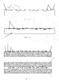
Figures 1a to 1c illustrate the method steps for producing a chuck according to the invention. -
Figure 2 illustrates a first bonding method according to the invention. -
Figure 3 illustrates a second bonding method according to the invention. - The compliant chuck according to the invention can be produced from a suitable flat substrate, for example a silicon wafer of 300 mm in diameter. Alternatively, a metal or ceramic substrate can be used.
Figure 1 illustrates the fabrication steps for producing a chuck according to a preferred embodiment, starting from a circular Si-wafer. As illustrated inFigure 1a , a number of alignment marks may first be produced on the top surface of thewafer 1. Two types of marks are produced :global alignment marks 2 are made along the circumference of the substrate's top surface, at a small distance a from the substrate's edge.Local alignment marks 3 are made around a plurality of dieplacement sites 4, distributed over the top surface. The plane view of the substrate shown inFigure 1a illustrates only a few of thedie placement sites 4, which normally cover the entirety of the surface in a predefined pattern. Thealignment marks 2/3 may be produced by any suitable technique. When the substrate is a silicon wafer, the marks may be produced by lithography, i.e. by etching in the silicon with a patterned photoresist layer as a mask. Alternatively, a laser ablation technique could be used. The global andlocal alignment marks 2/3 are preferably produced simultaneously. - Following this, as illustrated in
Figure 1b ,recesses 5 are etched in the substrate at the location of thedie placement sites 4. The depth of these recesses can be the same for all the placement sites, or this depth can vary between different placement sites, i.e. at least two sites have mutually different depths. A plurality of lithography steps with different masks can be used to obtain theserecesses 5 with varying depths. When therecesses 5 are made, the bottom surfaces of these recesses again qualify as 'die placement sites' within the context of this description. - Finally, carbon nanotube (CNT) films 6 are selectively grown on the bottom surface of the
recesses 5, as illustrated inFigure 1c . This can be done by depositing and patterning a catalyst layer on the substrate, so that the catalyst remains only on the bottom surface of each of therecesses 5. Growth of the CNT films is then established according to known CNT technology, until in each of the recesses a film is obtained consisting primarily of essentially vertically upstanding carbon nanotubes, with one end attached to the surface of the recess and the bodies of the nanotubes extending outward from said surface. The height of the tubes may be in the order of a few tens to a few hundreds of microns, in order to ensure sufficient resilience of the films 6 during operation. The level difference between different recesses may be anywhere between zero and a few hundred micron. - The preferred embodiment of the invention is a
chuck 10 as produced in the above-described way, wherein at least some of therecesses 5 are at multiple mutually different levels determined on the basis of a predefined pattern of dies of different thicknesses, which are to be collectively bonded to a target substrate by means of thechuck 10. The alignment marks 3 and 2 respectively enable accurate local alignment on die level and global alignment on wafer level. Therecesses 5 compensate for the height differences between the dies. The CNT films 6 provide a degree of compliance, by the fact that the vertical tubes have a degree of resilience when compressed in the longitudinal direction of the tubes. The compliance of the CNT films compensates any microscopic height differences that may not be compensated by the recesses or any non-planarities of the recesses and/or the dies. In this way, the combined effect of the recesses and the compliant CNT films results in a chuck that is suitable for use in collective bonding of dies, whilst having various advantages over known types of compliant chucks referred to above. The CNT films are capable of withstanding high operational temperature, pressure, and a high number of cycles of compression. The CNT material is also highly thermally conductive, so it can improve the thermal conduction from the chuck to the bonding interface during bonding. The CNT film can also provide a temporary adhesion which is high in shear direction but low in normal direction. - The CNT films maintain their resilience and adhesive force through many use cycles. According to a preferred embodiment, the CNT films are pre-compressed before the first use of the chuck. When the tubes are grown on the surface, they are formed as mutually parallel and essentially straight struts. When compressed, these struts buckle while remaining essentially parallel to each other, and quickly regain their original length when the compression force is removed. After a sufficiently high number of compression cycles, e.g. 1000 cycles, the compression, i.e. the buckled status of the struts, remains permanent. The result is that the tubes are permanently compressed to a thickness of for example 20% of their initial length. This phenomenon and the way in which to apply the cycles is described in
US7727624 , incorporated herein by reference. Alternatively, the permanent compression can also be achieved by applying a high force with much less cycles, e.g. 1 to a few cycles. When the film is partially pre-compressed, it is more stable during use of the chuck. - A first embodiment of a collective bonding method using a chuck according to the invention is illustrated in
Figure 2 . Dies 11 of different height are placed onto the CNT films of the chuck. This can be done by a known pick-and-place technique wherein the local alignment marks 3 are used for aligning each die to its respective location on the chuck. The dies are maintained on the chuck by the dry adhesive force exhibited by the CNT films. When placed on the chuck, the dies are substantially at the same upper level B given that therecesses 5 compensate for height differences between the dies and the depth of the recesses has been produced specifically as a function of a pre-defined pattern of dies with pre-defined heights. Possibly wafer level pre-treatment processes can be performed on the chuck while the dies are held by the adhesive force of the CNT films, such as wet cleaning or plasma treatments. Before bonding, the chuck is flipped and aligned to atarget wafer 12, by using the global alignment marks 2 on the chuck. The chuck is then moved closer to the target wafer until the dies are in contact with their target location on the target wafer and bonding can take place. Any type of bonding technique can be applied, such as direct bonding, Cu-Cu bonding, hybrid bonding etc. When the bond is established, release of the chuck is easily done by pulling the chuck away from the dies in the direction perpendicular to the dies. As the adhesive force exhibited by the CNT films is much lower in the normal direction than in the shear direction, a low pulling force is sufficient to release the chuck. - According to another embodiment, illustrated in
Figure 3 , the dies 11 are first placed on thetarget wafer 12 and temporarily maintained on their respective locations, e.g. by an underfill material. Thechuck 10 is then aligned to the target wafer by using the global alignment marks 2, and pushed down onto the dies. When the permanent bond is established, release of the chuck can again be done by a small normal force. For the latter embodiment, the local alignment marks 3 are not strictly required. - When all the dies that are to be bonded have the same height, the
recesses 5 can all have the same depth, as stated above, or the recess etch step may be skipped : the CNT films are then produced directly on thedie placement sites 4 on the surface of the substrate 1 (Figure 1a ). - In the above-described embodiment, the
chuck 10 has the same shape as thesubstrate 12 onto which the dies are to be bonded. This shape need not be circular but may also be rectangular for example. Alternatively, the chuck may have a smaller surface than the surface of the substrate onto which the dies are to be bonded, in order to be able to bond groups of dies to various areas of a target substrate. The shape of thedie placement sites 4/5 need not be the same for all die placement sites on the chuck. One chuck may comprise dieplacement sites 4/5 of different shapes, e.g. smaller and larger circles or smaller and larger squares or rectangles. - While the invention has been illustrated and described in detail in the drawings and foregoing description, such illustration and description are to be considered illustrative or exemplary and not restrictive. Other variations to the disclosed embodiments can be understood and effected by those skilled in the art in practicing the claimed invention, from a study of the drawings, the disclosure and the appended claims. In the claims, the word "comprising" does not exclude other elements or steps, and the indefinite article "a" or "an" does not exclude a plurality. The mere fact that certain measures are recited in mutually different dependent claims does not indicate that a combination of these measures cannot be used to advantage. Any reference signs in the claims should not be construed as limiting the scope.
- Unless specifically specified, the description of a layer being present, deposited or produced 'on' another layer or substrate, includes the options of
- said layer being present, produced or deposited directly on, i.e. in physical contact with, said other layer or substrate, and
- said layer being present, produced or deposited on one or a stack of intermediate layers between said layer and said other layer or substrate.
Claims (14)
- A chuck (10) for the bonding of a plurality of semiconductor dies to a target wafer (12), said chuck comprising a plurality of die placement sites (4,5), characterized in that said die placement sites comprise on their surface a resilient film (6) of carbon nanotubes (CNTs), said CNTs being attached to the surface of the die placement sites at one end and extending outwards from said surface.
- Chuck according to claim 1, wherein said die placement sites are formed as recesses (5) in a surface of the chuck (10).
- Chuck according to claim 2, wherein at least two of said recesses (5) have mutually different depths.
- Chuck according to any one of the preceding claims, further comprising a plurality of global alignment marks (2) for aligning the chuck to the target wafer (12).
- Chuck according to any one of claims 1 to 4, further comprising a plurality of local alignment marks (3) around said die placement sites (4,5), for aligning a die (11) with one of said die placement sites.
- Chuck according to any one of the preceding claims, wherein the carbon nanotubes of said CNT films (6) are pre-compressed.
- Method for producing a chuck (10) according to any one of the preceding claims, comprising the steps of :• Providing a substrate (1),• Defining a plurality of die placement sites (4,5) on a surface of the substrate,• Depositing a catalyst on said die placement sites (4,5),• growing a film (6) of carbon nanotubes on the catalyst.
- Method according to claim 7, wherein one or more of said die placement sites are defined by forming recesses (5) in said surface.
- Method according to claim 7 or 8, further comprising the step of producing global alignment marks (2) along the circumference of the substrate (1).
- Method according to any one of claims 7 to 9, further comprising the step of producing local alignment marks (3) around said die placement sites (4,5).
- Method according to any one of claims 7 to 10, further comprising the step of pre-compressing the carbon nanotubes of said CNT films.
- Method for collective bonding of a plurality of dies (11) to a target wafer (12), comprising the steps of :• Placing the dies (11) onto the CNT films (6) located on the die placement sites (4,5) of a chuck (10) according to any one of claims 1 to 6, wherein said dies are temporarily attached to the chuck by an adhesive force exhibited on the dies by the CNT films (6),• Aligning the chuck to the target wafer with the dies facing the target wafer,• Bonding the dies to the target wafer,• When the bond is established, removing the chuck by pulling the chuck away from the dies in a direction that is substantially perpendicular to the chuck.
- Method according to claim 12, further comprising the step of collectively treating the surface of the dies (11) on the chuck (10) by wet cleaning or plasma methods, before the steps of aligning and bonding.
- Method for collective bonding of a plurality of dies (11) to a target wafer (12), comprising the steps of :• Placing the dies (11) onto the target wafer (12) and maintaining the dies on said wafer by a temporary attachment means,• Aligning a chuck (10) according to any one of claims 1 to 6 to the target wafer (12) with the CNT films (6) facing the temporarily attached dies (11),• Bonding the dies to the target wafer while exerting a pressure on said dies by means of the chuck,• When the bond is established, removing the chuck by pulling the chuck away from the dies in a direction that is substantially perpendicular to the chuck.
Priority Applications (1)
| Application Number | Priority Date | Filing Date | Title |
|---|---|---|---|
| EP15185025.2A EP3029725B1 (en) | 2014-12-01 | 2015-09-14 | Chuck for collective bonding of semiconductor dies, method of making the same and methods of using the same |
Applications Claiming Priority (2)
| Application Number | Priority Date | Filing Date | Title |
|---|---|---|---|
| EP14195646 | 2014-12-01 | ||
| EP15185025.2A EP3029725B1 (en) | 2014-12-01 | 2015-09-14 | Chuck for collective bonding of semiconductor dies, method of making the same and methods of using the same |
Publications (2)
| Publication Number | Publication Date |
|---|---|
| EP3029725A1 true EP3029725A1 (en) | 2016-06-08 |
| EP3029725B1 EP3029725B1 (en) | 2019-10-30 |
Family
ID=51999333
Family Applications (1)
| Application Number | Title | Priority Date | Filing Date |
|---|---|---|---|
| EP15185025.2A Active EP3029725B1 (en) | 2014-12-01 | 2015-09-14 | Chuck for collective bonding of semiconductor dies, method of making the same and methods of using the same |
Country Status (2)
| Country | Link |
|---|---|
| EP (1) | EP3029725B1 (en) |
| CN (1) | CN105655282A (en) |
Cited By (4)
| Publication number | Priority date | Publication date | Assignee | Title |
|---|---|---|---|---|
| CN108878259A (en) * | 2017-05-15 | 2018-11-23 | Imec 非营利协会 | The method for forming dustproof film |
| CN115172192A (en) * | 2022-09-09 | 2022-10-11 | 之江实验室 | Hybrid bonding method for multi-core-grain wafer level integration |
| US20240047416A1 (en) * | 2020-12-10 | 2024-02-08 | Wuhan Xinxin Semiconductor Manufacturing Co., Ltd. | Chip-to-wafer stacking method |
| TWI897166B (en) * | 2023-11-08 | 2025-09-11 | 台灣積體電路製造股份有限公司 | Bonding tool and chip-on-wafer bonding process |
Citations (4)
| Publication number | Priority date | Publication date | Assignee | Title |
|---|---|---|---|---|
| US20070213419A1 (en) * | 2005-11-22 | 2007-09-13 | Rensselaer Polytechnic Institute | Super-compressible carbon nanotube films and micro-bundles |
| US20100123268A1 (en) * | 2008-11-19 | 2010-05-20 | Etienne Menard | Printing Semiconductor Elements by Shear-Assisted Elastomeric Stamp Transfer |
| US20130210194A1 (en) * | 2012-02-09 | 2013-08-15 | LuxVue Technology Corporation | Method of transferring and bonding an array of micro devices |
| US20130327811A1 (en) * | 2012-06-12 | 2013-12-12 | International Business Machines Corporation | Three dimensional flip chip system and method |
Family Cites Families (3)
| Publication number | Priority date | Publication date | Assignee | Title |
|---|---|---|---|---|
| US8398909B1 (en) * | 2008-09-18 | 2013-03-19 | Carnegie Mellon University | Dry adhesives and methods of making dry adhesives |
| US8349653B2 (en) * | 2010-06-02 | 2013-01-08 | Maxim Integrated Products, Inc. | Use of device assembly for a generalization of three-dimensional metal interconnect technologies |
| WO2013096730A1 (en) * | 2011-12-22 | 2013-06-27 | Carnegie Mellon University | Methods, apparatuses, and systems for micromanipulation with adhesive fibrillar structures |
-
2015
- 2015-09-14 EP EP15185025.2A patent/EP3029725B1/en active Active
- 2015-11-27 CN CN201510852638.2A patent/CN105655282A/en not_active Withdrawn
Patent Citations (5)
| Publication number | Priority date | Publication date | Assignee | Title |
|---|---|---|---|---|
| US20070213419A1 (en) * | 2005-11-22 | 2007-09-13 | Rensselaer Polytechnic Institute | Super-compressible carbon nanotube films and micro-bundles |
| US7727624B2 (en) | 2005-11-22 | 2010-06-01 | Rensselaer Polytechnic Institute | Super-compressible carbon nanotube films and micro-bundles |
| US20100123268A1 (en) * | 2008-11-19 | 2010-05-20 | Etienne Menard | Printing Semiconductor Elements by Shear-Assisted Elastomeric Stamp Transfer |
| US20130210194A1 (en) * | 2012-02-09 | 2013-08-15 | LuxVue Technology Corporation | Method of transferring and bonding an array of micro devices |
| US20130327811A1 (en) * | 2012-06-12 | 2013-12-12 | International Business Machines Corporation | Three dimensional flip chip system and method |
Cited By (4)
| Publication number | Priority date | Publication date | Assignee | Title |
|---|---|---|---|---|
| CN108878259A (en) * | 2017-05-15 | 2018-11-23 | Imec 非营利协会 | The method for forming dustproof film |
| US20240047416A1 (en) * | 2020-12-10 | 2024-02-08 | Wuhan Xinxin Semiconductor Manufacturing Co., Ltd. | Chip-to-wafer stacking method |
| CN115172192A (en) * | 2022-09-09 | 2022-10-11 | 之江实验室 | Hybrid bonding method for multi-core-grain wafer level integration |
| TWI897166B (en) * | 2023-11-08 | 2025-09-11 | 台灣積體電路製造股份有限公司 | Bonding tool and chip-on-wafer bonding process |
Also Published As
| Publication number | Publication date |
|---|---|
| EP3029725B1 (en) | 2019-10-30 |
| CN105655282A (en) | 2016-06-08 |
Similar Documents
| Publication | Publication Date | Title |
|---|---|---|
| JP7490108B2 (en) | Substrate structuring method | |
| US10679884B2 (en) | Film electrode for electrostatic chuck | |
| EP3029725B1 (en) | Chuck for collective bonding of semiconductor dies, method of making the same and methods of using the same | |
| EP2267761A2 (en) | Graphene wafer, method for manufacturing the graphene wafer, method for releasing a graphene layer, and method for manufacturing a graphene device | |
| US11121117B2 (en) | Method for self-assembling microelectronic components | |
| US10950462B2 (en) | Diamond substrate producing method | |
| EP2747132B1 (en) | A method for transferring a graphene sheet to metal contact bumps of a substrate for use in semiconductor device package | |
| CN103811419A (en) | Semiconductor die singulation method and apparatus | |
| CN110349912B (en) | Method for coupling a semiconductor component to a target substrate by transfer printing | |
| JP6441181B2 (en) | Imprint template, method for manufacturing the same, and method for manufacturing a semiconductor device | |
| CN113228319B (en) | Method for transferring surface layer to cavity | |
| CN104662649B (en) | Direct Bonding technique | |
| KR102656505B1 (en) | Die-to-wafer bonding utilizing micro-transfer printing | |
| JP5187705B2 (en) | Anisotropic etching method, three-dimensional structure, and device | |
| KR101467390B1 (en) | Method of manufacturing an adhesion pad | |
| KR102158176B1 (en) | Semiconductor substrate having a GaN-based thin film layer connected by fine pillar AND method for manufacturing the same | |
| JP6085757B2 (en) | Fabrication method of microstructure | |
| CN119517737A (en) | A method for preparing carbon-based semiconductor thin film material | |
| KR101386004B1 (en) | Method of Fabricating Micro-Grid Structure using Wafer Bonding Techniques | |
| JP2006323088A (en) | Manufacturing method of donor substrate and minute structure, and donor substrate | |
| JP2007335546A (en) | Mold fabrication method | |
| JP2005055582A (en) | Method for manufacturing three-dimensional layered structural body |
Legal Events
| Date | Code | Title | Description |
|---|---|---|---|
| PUAI | Public reference made under article 153(3) epc to a published international application that has entered the european phase |
Free format text: ORIGINAL CODE: 0009012 |
|
| AK | Designated contracting states |
Kind code of ref document: A1 Designated state(s): AL AT BE BG CH CY CZ DE DK EE ES FI FR GB GR HR HU IE IS IT LI LT LU LV MC MK MT NL NO PL PT RO RS SE SI SK SM TR |
|
| AX | Request for extension of the european patent |
Extension state: BA ME |
|
| STAA | Information on the status of an ep patent application or granted ep patent |
Free format text: STATUS: REQUEST FOR EXAMINATION WAS MADE |
|
| 17P | Request for examination filed |
Effective date: 20161201 |
|
| RBV | Designated contracting states (corrected) |
Designated state(s): AL AT BE BG CH CY CZ DE DK EE ES FI FR GB GR HR HU IE IS IT LI LT LU LV MC MK MT NL NO PL PT RO RS SE SI SK SM TR |
|
| GRAP | Despatch of communication of intention to grant a patent |
Free format text: ORIGINAL CODE: EPIDOSNIGR1 |
|
| STAA | Information on the status of an ep patent application or granted ep patent |
Free format text: STATUS: GRANT OF PATENT IS INTENDED |
|
| RIC1 | Information provided on ipc code assigned before grant |
Ipc: H01L 21/67 20060101ALI20190405BHEP Ipc: H01L 21/60 20060101ALI20190405BHEP Ipc: H01L 23/00 20060101AFI20190405BHEP |
|
| INTG | Intention to grant announced |
Effective date: 20190430 |
|
| GRAS | Grant fee paid |
Free format text: ORIGINAL CODE: EPIDOSNIGR3 |
|
| GRAA | (expected) grant |
Free format text: ORIGINAL CODE: 0009210 |
|
| STAA | Information on the status of an ep patent application or granted ep patent |
Free format text: STATUS: THE PATENT HAS BEEN GRANTED |
|
| AK | Designated contracting states |
Kind code of ref document: B1 Designated state(s): AL AT BE BG CH CY CZ DE DK EE ES FI FR GB GR HR HU IE IS IT LI LT LU LV MC MK MT NL NO PL PT RO RS SE SI SK SM TR |
|
| REG | Reference to a national code |
Ref country code: GB Ref legal event code: FG4D |
|
| REG | Reference to a national code |
Ref country code: CH Ref legal event code: EP |
|
| REG | Reference to a national code |
Ref country code: AT Ref legal event code: REF Ref document number: 1197063 Country of ref document: AT Kind code of ref document: T Effective date: 20191115 |
|
| REG | Reference to a national code |
Ref country code: DE Ref legal event code: R096 Ref document number: 602015040604 Country of ref document: DE |
|
| REG | Reference to a national code |
Ref country code: IE Ref legal event code: FG4D |
|
| REG | Reference to a national code |
Ref country code: LT Ref legal event code: MG4D |
|
| PG25 | Lapsed in a contracting state [announced via postgrant information from national office to epo] |
Ref country code: PT Free format text: LAPSE BECAUSE OF FAILURE TO SUBMIT A TRANSLATION OF THE DESCRIPTION OR TO PAY THE FEE WITHIN THE PRESCRIBED TIME-LIMIT Effective date: 20200302 Ref country code: FI Free format text: LAPSE BECAUSE OF FAILURE TO SUBMIT A TRANSLATION OF THE DESCRIPTION OR TO PAY THE FEE WITHIN THE PRESCRIBED TIME-LIMIT Effective date: 20191030 Ref country code: BG Free format text: LAPSE BECAUSE OF FAILURE TO SUBMIT A TRANSLATION OF THE DESCRIPTION OR TO PAY THE FEE WITHIN THE PRESCRIBED TIME-LIMIT Effective date: 20200130 Ref country code: SE Free format text: LAPSE BECAUSE OF FAILURE TO SUBMIT A TRANSLATION OF THE DESCRIPTION OR TO PAY THE FEE WITHIN THE PRESCRIBED TIME-LIMIT Effective date: 20191030 Ref country code: LV Free format text: LAPSE BECAUSE OF FAILURE TO SUBMIT A TRANSLATION OF THE DESCRIPTION OR TO PAY THE FEE WITHIN THE PRESCRIBED TIME-LIMIT Effective date: 20191030 Ref country code: LT Free format text: LAPSE BECAUSE OF FAILURE TO SUBMIT A TRANSLATION OF THE DESCRIPTION OR TO PAY THE FEE WITHIN THE PRESCRIBED TIME-LIMIT Effective date: 20191030 Ref country code: NO Free format text: LAPSE BECAUSE OF FAILURE TO SUBMIT A TRANSLATION OF THE DESCRIPTION OR TO PAY THE FEE WITHIN THE PRESCRIBED TIME-LIMIT Effective date: 20200130 Ref country code: PL Free format text: LAPSE BECAUSE OF FAILURE TO SUBMIT A TRANSLATION OF THE DESCRIPTION OR TO PAY THE FEE WITHIN THE PRESCRIBED TIME-LIMIT Effective date: 20191030 Ref country code: GR Free format text: LAPSE BECAUSE OF FAILURE TO SUBMIT A TRANSLATION OF THE DESCRIPTION OR TO PAY THE FEE WITHIN THE PRESCRIBED TIME-LIMIT Effective date: 20200131 Ref country code: NL Free format text: LAPSE BECAUSE OF FAILURE TO SUBMIT A TRANSLATION OF THE DESCRIPTION OR TO PAY THE FEE WITHIN THE PRESCRIBED TIME-LIMIT Effective date: 20191030 |
|
| REG | Reference to a national code |
Ref country code: NL Ref legal event code: MP Effective date: 20191030 |
|
| PG25 | Lapsed in a contracting state [announced via postgrant information from national office to epo] |
Ref country code: HR Free format text: LAPSE BECAUSE OF FAILURE TO SUBMIT A TRANSLATION OF THE DESCRIPTION OR TO PAY THE FEE WITHIN THE PRESCRIBED TIME-LIMIT Effective date: 20191030 Ref country code: IS Free format text: LAPSE BECAUSE OF FAILURE TO SUBMIT A TRANSLATION OF THE DESCRIPTION OR TO PAY THE FEE WITHIN THE PRESCRIBED TIME-LIMIT Effective date: 20200229 Ref country code: RS Free format text: LAPSE BECAUSE OF FAILURE TO SUBMIT A TRANSLATION OF THE DESCRIPTION OR TO PAY THE FEE WITHIN THE PRESCRIBED TIME-LIMIT Effective date: 20191030 |
|
| PG25 | Lapsed in a contracting state [announced via postgrant information from national office to epo] |
Ref country code: AL Free format text: LAPSE BECAUSE OF FAILURE TO SUBMIT A TRANSLATION OF THE DESCRIPTION OR TO PAY THE FEE WITHIN THE PRESCRIBED TIME-LIMIT Effective date: 20191030 |
|
| PG25 | Lapsed in a contracting state [announced via postgrant information from national office to epo] |
Ref country code: EE Free format text: LAPSE BECAUSE OF FAILURE TO SUBMIT A TRANSLATION OF THE DESCRIPTION OR TO PAY THE FEE WITHIN THE PRESCRIBED TIME-LIMIT Effective date: 20191030 Ref country code: DK Free format text: LAPSE BECAUSE OF FAILURE TO SUBMIT A TRANSLATION OF THE DESCRIPTION OR TO PAY THE FEE WITHIN THE PRESCRIBED TIME-LIMIT Effective date: 20191030 Ref country code: RO Free format text: LAPSE BECAUSE OF FAILURE TO SUBMIT A TRANSLATION OF THE DESCRIPTION OR TO PAY THE FEE WITHIN THE PRESCRIBED TIME-LIMIT Effective date: 20191030 Ref country code: CZ Free format text: LAPSE BECAUSE OF FAILURE TO SUBMIT A TRANSLATION OF THE DESCRIPTION OR TO PAY THE FEE WITHIN THE PRESCRIBED TIME-LIMIT Effective date: 20191030 Ref country code: ES Free format text: LAPSE BECAUSE OF FAILURE TO SUBMIT A TRANSLATION OF THE DESCRIPTION OR TO PAY THE FEE WITHIN THE PRESCRIBED TIME-LIMIT Effective date: 20191030 |
|
| REG | Reference to a national code |
Ref country code: DE Ref legal event code: R097 Ref document number: 602015040604 Country of ref document: DE |
|
| REG | Reference to a national code |
Ref country code: AT Ref legal event code: MK05 Ref document number: 1197063 Country of ref document: AT Kind code of ref document: T Effective date: 20191030 |
|
| PG25 | Lapsed in a contracting state [announced via postgrant information from national office to epo] |
Ref country code: SM Free format text: LAPSE BECAUSE OF FAILURE TO SUBMIT A TRANSLATION OF THE DESCRIPTION OR TO PAY THE FEE WITHIN THE PRESCRIBED TIME-LIMIT Effective date: 20191030 Ref country code: IT Free format text: LAPSE BECAUSE OF FAILURE TO SUBMIT A TRANSLATION OF THE DESCRIPTION OR TO PAY THE FEE WITHIN THE PRESCRIBED TIME-LIMIT Effective date: 20191030 Ref country code: SK Free format text: LAPSE BECAUSE OF FAILURE TO SUBMIT A TRANSLATION OF THE DESCRIPTION OR TO PAY THE FEE WITHIN THE PRESCRIBED TIME-LIMIT Effective date: 20191030 |
|
| PLBE | No opposition filed within time limit |
Free format text: ORIGINAL CODE: 0009261 |
|
| STAA | Information on the status of an ep patent application or granted ep patent |
Free format text: STATUS: NO OPPOSITION FILED WITHIN TIME LIMIT |
|
| 26N | No opposition filed |
Effective date: 20200731 |
|
| PG25 | Lapsed in a contracting state [announced via postgrant information from national office to epo] |
Ref country code: AT Free format text: LAPSE BECAUSE OF FAILURE TO SUBMIT A TRANSLATION OF THE DESCRIPTION OR TO PAY THE FEE WITHIN THE PRESCRIBED TIME-LIMIT Effective date: 20191030 Ref country code: SI Free format text: LAPSE BECAUSE OF FAILURE TO SUBMIT A TRANSLATION OF THE DESCRIPTION OR TO PAY THE FEE WITHIN THE PRESCRIBED TIME-LIMIT Effective date: 20191030 |
|
| REG | Reference to a national code |
Ref country code: DE Ref legal event code: R119 Ref document number: 602015040604 Country of ref document: DE |
|
| PG25 | Lapsed in a contracting state [announced via postgrant information from national office to epo] |
Ref country code: MC Free format text: LAPSE BECAUSE OF FAILURE TO SUBMIT A TRANSLATION OF THE DESCRIPTION OR TO PAY THE FEE WITHIN THE PRESCRIBED TIME-LIMIT Effective date: 20191030 |
|
| REG | Reference to a national code |
Ref country code: CH Ref legal event code: PL |
|
| GBPC | Gb: european patent ceased through non-payment of renewal fee |
Effective date: 20200914 |
|
| REG | Reference to a national code |
Ref country code: BE Ref legal event code: MM Effective date: 20200930 |
|
| PG25 | Lapsed in a contracting state [announced via postgrant information from national office to epo] |
Ref country code: LU Free format text: LAPSE BECAUSE OF NON-PAYMENT OF DUE FEES Effective date: 20200914 |
|
| PG25 | Lapsed in a contracting state [announced via postgrant information from national office to epo] |
Ref country code: FR Free format text: LAPSE BECAUSE OF NON-PAYMENT OF DUE FEES Effective date: 20200930 Ref country code: DE Free format text: LAPSE BECAUSE OF NON-PAYMENT OF DUE FEES Effective date: 20210401 |
|
| PG25 | Lapsed in a contracting state [announced via postgrant information from national office to epo] |
Ref country code: BE Free format text: LAPSE BECAUSE OF NON-PAYMENT OF DUE FEES Effective date: 20200930 Ref country code: CH Free format text: LAPSE BECAUSE OF NON-PAYMENT OF DUE FEES Effective date: 20200930 Ref country code: GB Free format text: LAPSE BECAUSE OF NON-PAYMENT OF DUE FEES Effective date: 20200914 Ref country code: LI Free format text: LAPSE BECAUSE OF NON-PAYMENT OF DUE FEES Effective date: 20200930 Ref country code: IE Free format text: LAPSE BECAUSE OF NON-PAYMENT OF DUE FEES Effective date: 20200914 |
|
| PG25 | Lapsed in a contracting state [announced via postgrant information from national office to epo] |
Ref country code: TR Free format text: LAPSE BECAUSE OF FAILURE TO SUBMIT A TRANSLATION OF THE DESCRIPTION OR TO PAY THE FEE WITHIN THE PRESCRIBED TIME-LIMIT Effective date: 20191030 Ref country code: MT Free format text: LAPSE BECAUSE OF FAILURE TO SUBMIT A TRANSLATION OF THE DESCRIPTION OR TO PAY THE FEE WITHIN THE PRESCRIBED TIME-LIMIT Effective date: 20191030 Ref country code: CY Free format text: LAPSE BECAUSE OF FAILURE TO SUBMIT A TRANSLATION OF THE DESCRIPTION OR TO PAY THE FEE WITHIN THE PRESCRIBED TIME-LIMIT Effective date: 20191030 |
|
| PG25 | Lapsed in a contracting state [announced via postgrant information from national office to epo] |
Ref country code: MK Free format text: LAPSE BECAUSE OF FAILURE TO SUBMIT A TRANSLATION OF THE DESCRIPTION OR TO PAY THE FEE WITHIN THE PRESCRIBED TIME-LIMIT Effective date: 20191030 |