EP3026443A1 - An electronic device for measuring a differential current in an electric line. - Google Patents
An electronic device for measuring a differential current in an electric line. Download PDFInfo
- Publication number
- EP3026443A1 EP3026443A1 EP14195071.7A EP14195071A EP3026443A1 EP 3026443 A1 EP3026443 A1 EP 3026443A1 EP 14195071 A EP14195071 A EP 14195071A EP 3026443 A1 EP3026443 A1 EP 3026443A1
- Authority
- EP
- European Patent Office
- Prior art keywords
- signal
- signal processing
- electronic device
- differential current
- processing means
- Prior art date
- Legal status (The legal status is an assumption and is not a legal conclusion. Google has not performed a legal analysis and makes no representation as to the accuracy of the status listed.)
- Granted
Links
Images








Classifications
-
- G—PHYSICS
- G01—MEASURING; TESTING
- G01R—MEASURING ELECTRIC VARIABLES; MEASURING MAGNETIC VARIABLES
- G01R19/00—Arrangements for measuring currents or voltages or for indicating presence or sign thereof
- G01R19/0092—Measuring current only
-
- G—PHYSICS
- G01—MEASURING; TESTING
- G01R—MEASURING ELECTRIC VARIABLES; MEASURING MAGNETIC VARIABLES
- G01R15/00—Details of measuring arrangements of the types provided for in groups G01R17/00 - G01R29/00, G01R33/00 - G01R33/26 or G01R35/00
- G01R15/14—Adaptations providing voltage or current isolation, e.g. for high-voltage or high-current networks
- G01R15/18—Adaptations providing voltage or current isolation, e.g. for high-voltage or high-current networks using inductive devices, e.g. transformers
- G01R15/183—Adaptations providing voltage or current isolation, e.g. for high-voltage or high-current networks using inductive devices, e.g. transformers using transformers with a magnetic core
-
- H—ELECTRICITY
- H01—ELECTRIC ELEMENTS
- H01H—ELECTRIC SWITCHES; RELAYS; SELECTORS; EMERGENCY PROTECTIVE DEVICES
- H01H83/00—Protective switches, e.g. circuit-breaking switches, or protective relays operated by abnormal electrical conditions otherwise than solely by excess current
- H01H83/20—Protective switches, e.g. circuit-breaking switches, or protective relays operated by abnormal electrical conditions otherwise than solely by excess current operated by excess current as well as by some other abnormal electrical condition
- H01H83/22—Protective switches, e.g. circuit-breaking switches, or protective relays operated by abnormal electrical conditions otherwise than solely by excess current operated by excess current as well as by some other abnormal electrical condition the other condition being imbalance of two or more currents or voltages
- H01H83/226—Protective switches, e.g. circuit-breaking switches, or protective relays operated by abnormal electrical conditions otherwise than solely by excess current operated by excess current as well as by some other abnormal electrical condition the other condition being imbalance of two or more currents or voltages with differential transformer
-
- Y—GENERAL TAGGING OF NEW TECHNOLOGICAL DEVELOPMENTS; GENERAL TAGGING OF CROSS-SECTIONAL TECHNOLOGIES SPANNING OVER SEVERAL SECTIONS OF THE IPC; TECHNICAL SUBJECTS COVERED BY FORMER USPC CROSS-REFERENCE ART COLLECTIONS [XRACs] AND DIGESTS
- Y02—TECHNOLOGIES OR APPLICATIONS FOR MITIGATION OR ADAPTATION AGAINST CLIMATE CHANGE
- Y02E—REDUCTION OF GREENHOUSE GAS [GHG] EMISSIONS, RELATED TO ENERGY GENERATION, TRANSMISSION OR DISTRIBUTION
- Y02E10/00—Energy generation through renewable energy sources
- Y02E10/50—Photovoltaic [PV] energy
Definitions
- the present invention relates to an electronic device for measuring a differential current in an electric line.
- the electronic device of the invention is particularly suitable for low or medium voltage applications, where the term “low voltage” (LV) relates to voltages lower than 1 kV AC and 1.5 kV DC and the term “medium voltage” (MV) relates to voltages higher than 1 kV AC and 1.5 kV DC up to some tens of kV, e.g. up to 72 kV AC and 100 kV DC.
- LV low voltage
- MV medium voltage
- differential currents may, in fact, be indicative of occurring fault conditions.
- protection devices are known, which are capable to detect the presence of AC or DC differential currents in an electric line.
- the main aim of the present invention is to provide an electronic device for measuring a differential current in an electric line, which allows overcoming limitations of current solutions of the state of the art.
- an object of the present invention is to provide an electronic device that is capable of detecting a differential current in an electric line and providing quantitative information (measuring signals) about the detected differential current.
- a further object of the present invention is to provide an electronic device that offers outstanding performances in terms of flexibility of use.
- Yet another object of the present invention is to provide an electronic device that is relatively easy and cheap to manufacture at industrial level.
- the present invention thus provides an electronic device for measuring a differential current in an electric line, according to the following claim 1 and the related dependent claims.
- the electronic device is capable of detecting and measuring a time-invariant component of a differential current among the conductors of an electric line, such as, for example, a leakage current caused by the deterioration of an electric insulation arrangement or by the failure of components connected to ground.
- the electronic device is capable of providing information indicative of the absolute value and the flowing direction of a time-invariant component of a differential current among the conductors of an electric line.
- the electronic device is also capable of detecting and measuring a time-variant component of a differential current among the conductors of an electric line, such as, for example, a ground fault current.
- time-invariant component and “time-variant component” of a differential current respectively mean a DC component and an AC component of said differential current.
- a differential current in an electric line may include only a DC current or only AC current or, more frequently, is the result of the superimposition of AC and DC currents.
- AC currents not having a sine wave-form but showing periodic variations (e.g. pulsed currents, partialized currents or the like) are here considered as AC currents.
- the electronic device is capable of detecting a differential current in an electric line, decomposing the detected differential current in its DC and AC components and providing measuring signals indicative of each of said components.
- the quantitative information about the time-invariant and time-variant components of a differential current in an electric line may be conveniently exploited in many kinds of LV and MV applications.
- information collected by measuring the time-invariant component of a detected differential current may be used to compensate small intrinsic DC earth leakages occurring during normal operating conditions or to ensure a correct operation of protection devices positioned upstream with respect to the point of the installation at which said DC earth leakages occur.
- measurement information about the time-invariant and time variant components of a differential current may be used to practically implement advanced protection or fault-management strategies. Further aspects of the invention relate to an electronic arrangement for LV or MV applications, according to the following claims 13 and 14.
- a further aspect of the invention relates to a photovoltaic electric power generation system, according to the following claim 15.
- a further aspect of the invention relates to a LV or MV electric power distribution system or network, according to the following claim 16.
- the present invention relates to an electronic device 1 for measuring a differential current ID in a LV or MV electric line 100.
- the electric line 100 may be, for example, an electric power supply line of an electric power distribution network or a battery charging system for electric vehicles.
- the electric line 100 comprises a plurality of conductors and it may be, for example, of the single or multi-phase type.
- the electronic device 1 comprises a sensing circuit 2 operatively coupled to the conductors of the electric line 100.
- the sensing circuit 2 advantageously comprises a current transformer 21 provided with a magnetic core 211, preferably shaped as a toroid.
- the magnetic core 211 has a high magnetic permeability and it may be made, for example, of a Ni-Fe alloy.
- the transformer 21 is advantageously arranged to sense unbalancing currents among the conductors of the electric line 100.
- the conductors of the electric line 100 pass through the magnetic core 211 so as to form the primary winding for the transformer 21.
- the conductors of the primary line 100 may be wound around the magnetic core 211 to form multiple turns, for example 3 turns.
- the transformer 21 has a secondary winding 212 that is advantageously wound around the magnetic core 211 with a relatively high number of turns, for example 250 turns.
- the transformer 21 further comprises an excitation winding 213, which is advantageously wound around the magnetic core 211 with a relatively high number of turns, for example 250 turns.
- an AC excitation current IE circulates along the excitation winding 213.
- the excitation current IE may be advantageously generated by a generation circuit 214 that may be of the known type, for example an electronic oscillator circuit.
- the excitation current IE may have a frequency of 500 Hz and a waveform that may be, for example, sinusoidal.
- the excitation current IE polarizes the magnetic core 211 of the transformer 21 at an operating point in which the magnetic permeability of the magnetic core 211 shows a strong transition towards small values, namely at an operating point located close a positive or negative saturation region of the hysteresis loop of the magnetic core 211.
- the sensing circuit 2 comprises an output circuit section 22 electrically connected to the secondary winding 212 of the transformer 21.
- the output circuit section 22 is configured to provide a first signal V1 (preferably a voltage signal) indicative of the differential current ID. Basically, it receives a current circulating along the secondary winding 212 and generates the signal V1.
- V1 preferably a voltage signal
- the output circuit section 22 may advantageously comprise a resistive circuit (e.g. a shunt-resistor connected between a terminal of the secondary winding and ground) to generate the signal V1.
- a resistive circuit e.g. a shunt-resistor connected between a terminal of the secondary winding and ground
- Figures 14-17 show some experimental measurements of the signal V1 in different operative conditions.
- the signal V1 is basically an AC signal comprising a fixed AC signal component FSC due to circulation of the excitation current IE along the excitation winding 213.
- the signal V1 basically depends on the waveform and carrier frequency of the excitation current IE only ( figure 14 ).
- the signal V1 When it is present a differential current ID having only a time-invariant component, the signal V1 has the same frequency of the excitation current IE but it may show first amplitude over-shoots OS1 occurring with multiple frequencies of the excitation current IE ( figure 15 ).
- the amplitude over-shoots OS1 may be positive or negative depending on the direction of the current ID.
- the signal V1 When it is present a differential current ID having only a time-variant component, the signal V1 has the same carrier frequency of the excitation current IE but it may show a waveform modulated in amplitude and second amplitude over-shoots OS2 occurring with frequencies different from the frequency of the excitation current IE ( figure 16 ).
- the amplitude over-shoots OS2 may be positive and/or negative.
- the voltage V1 When it is present a differential current ID having both time-invariant and time-variant components, the voltage V1 has the same carrier frequency of the excitation current IE but it may show a waveform possibly modulated in amplitude and having amplitude overshoots induced by the nonlinear, saturating behaviour of the magnetic material of the magnetic core 211.
- the waveform may have the first and second amplitude overshoots OS1, OS2 described above.
- the waveform may have higher and lower amplitude over-shoots OS2 (positive and/or negative) occurring with frequencies different from the frequency of the excitation current IE.
- the electronic device 1 comprises first signal processing means 3 configured to process the signal V1.
- the signal processing means 3 provide a second signal VD (preferably a voltage signal) indicative of a differential current ID detected by the sensing circuit 2.
- the signal VD When no differential current ID is present among the conductors of the electric line 100, the signal VD has amplitude substantially null (e.g. 0.4V).
- the signal VD is substantially a function of the time-invariant and time-variant components of the differential current ID.
- the signal processing means 3 are configured so that they provide a signal VD that is more sensitive to the time-invariant component of the differential current ID.
- the electronic device 1 comprises second signal processing means 4 configured to process the second signal VD.
- the second signal processing means 4 provide a first measurement signal IDCM indicative of the absolute value of a time-invariant component of a differential current ID detected by the sensing circuit 2.
- the measurement error Err is relatively small for most of the applications in which the electronic device 1 may be adopted.
- the measurement error Err can thus be neglected without prejudice for the overall reliability of the electronic device 1.
- the electronic device 1 comprises third signal processing means 5 configured to process the signal V1.
- the signal processing means 5 provide third and fourth signals S1, S2 (preferably voltage signals) that indicate whether the magnetic core 211 of the transformer 21 operates in a positive or in a negative saturation region of its own hysteresis loop, when the differential current ID has a time-invariant current component that is not null.
- S1, S2 preferably voltage signals
- the signal processing means 5 are advantageously configured to provide information on the non-linear effect produced on the magnetic core 211 by said time-invariant component.
- a magnetic field is present due to the superimposition of a magnetic field generated by the excitation current IE and a magnetic field generated by the differential current ID.
- Such a magnetic field may be prevalently positive or negative depending on whether the time-invariant component of the differential current ID is respectively positive or negative (according to a given sign convention).
- Signals S1, S2 are indicative of such a non-linear behaviour of the magnetic core 211 and thus can be used to obtain information on the flowing direction (sign) of the time-invariant component of a differential current ID among the conductors of the electric line 100.
- the electronic device 1 comprises fourth signal processing means 6 configured to process the third and fourth signals S1, S2.
- the signal processing means 6 provide a second measurement signal SDC indicative of the direction of the time-invariant component of a differential current ID detected by the sensing circuit 2.
- a prevalently positive or negative magnetic field may be present in the magnetic core 211 of the transformer 21, when a differential current ID is present among the conductors of the electric line 100.
- the non-linear effect produced on the magnetic core 211 by the time-invariant component of the differential current ID may be high, moderate or low.
- the signal processing means 6 process the signals S1, S2 to provide information R1, R2 indicating whether the intensity of the signals S1, S2 is at a high, moderate or low level ( figures 11-12 ).
- the signal processing means 6 process such information R1, R2 to determine the sign of the time-invariant component of the differential current ID.
- the sign of the time-invariant component of the differential current ID cannot be determined because the non-linear effect produced on the magnetic core 211 is null or too moderate.
- the electronic device 1 may comprise fifth signal processing means 10 configured to process the measurement signals IDCM and SDC and provide a fourth measurement signal IDC indicative of the time-invariant component (with its sign) of a detected differential current ID.
- the quantitative information IDC may be calculated on the base of measurement data IDCM, SDC.
- the electronic device 1 is also capable of providing quantitative information IAC about the time-variant component of a detected differential current ID.
- the electronic device 1 comprises sixth signal processing means 7 configured to process the first signal V1 and provide a fifth signal VD2 (preferably a voltage signal) indicative of the differential current ID.
- VD2 preferably a voltage signal
- the signal VD2 is substantially a function of the time-invariant and time-variant components of the differential current ID.
- the signal processing means 7 are configured so that they provide a signal VD2 that is more sensitive to the time-variant component of the differential current ID.
- the electronic device 1 comprises seventh signal processing means 8 configured to process the fifth signal VD2 and provide a third measurement signal IDM indicative of the absolute value of the differential current ID.
- the signal processing means 3 are advantageously configured to provide a sixth signal VD3 (preferably a voltage signal) indicative of the differential current ID.
- the sixth signal VD3 may coincide with the second signal VD.
- the electronic device 1 comprises eighth signal processing means 9 configured to process the signal VD3 and provide the third measurement signal IDM.
- the fifth signal processing means 10 are also configured to process the measurement signals IDCM, IDM and provide a fifth measurement signal IAC indicative of the time-variant component of the differential current ID.
- the quantitative information IAC may be complementary calculated on the base of measurement data IDCM, IDM.
- the electronic device 1 is also capable of providing quantitative information IDT about a detected differential current ID.
- the signal processing means 10 are also configured to process the measurement signals IDCM, SDC, IDM and provide a sixth measurement signal IDT indicative of the overall differential current ID present between the conductors of the electric line 100.
- the processing means 10 may be configured to process the measurement signals IDCM, SDC and the signal V1 in order to provide the measurement signal IAC and/or the measurement signal IDT.
- the signal processing means 3, 4, 5, 6, 7, 8, 9, 10 may be industrially implemented in an analog and/or digital manner.
- circuits suitably arranged to perform the functions of said processing means.
- Said electronic circuits may form separated circuit units or may be at least partially integrated in one or more circuit units.
- they comprise suitably arranged software instructions stored in a medium and executable by one or more computerised units (e.g. microprocessors) to perform the functions of said processing means.
- computerised units e.g. microprocessors
- the first signal processing means 3 preferably comprise a first signal processing module 31 configured to perform an amplitude filtering of the signal V1.
- the signal processing module 31 provides in output a first intermediate signal VI1 (preferably a voltage signal), which is a function of the time-invariant and time-variant components of a differential current ID circulating among the conductors of the electric line 100.
- a first intermediate signal VI1 preferably a voltage signal
- the signal processing module 31 is advantageously configured to cut-off the fixed AC signal component FSC that is due to the circulation of the excitation current IE along the excitation winding 213.
- the first signal processing module 31 comprises a diode bridge circuit 311 and a cascade of amplifying circuits 312, 313 electrically connected to the diode bridge circuit 311.
- the amplifying circuit 312 comprises an operation amplifier 3120 arranged in a known manner to provide amplification functionalities.
- the operational amplifier 3120 may be electrically connected to a resistive network 3121 and a resistive-capacitive network 3122.
- the amplifying circuit 313 may comprise an operation amplifier 3130 that may be arranged in a known manner to provide amplification functionalities.
- the operational amplifier 3130 may be electrically connected to a resistive network 3131 and a resistive-capacitive network 3132.
- the signal processing module 31 comprises an output filtering circuit 314 (e.g. of capacitive type in a known configuration) to filter undesired frequency components of the signal VI1.
- an output filtering circuit 314 e.g. of capacitive type in a known configuration
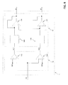
- the diode bridge circuit 311, the amplifying circuit 312, the amplifying circuit 313 and the output filtering circuit 314 are electrically connected in series according to the configuration shown in figure 4 .
- the position of the diode bridge circuit 311 and of the amplifying circuits 312, 313 may be inverted.
- the first signal processing means 3 preferably comprise a second signal processing module 32 configured to perform a wave-form rectification of the signal VI1 provided in output by the signal processing module 31.
- the signal processing module 32 provides a second intermediate signal VI2 (preferably a voltage signal), which is a rectified signal.
- the second signal processing module 32 may comprise an operation amplifier 320 arranged in a known manner to provide rectification functionalities.
- the operational amplifier 320 may be suitably electrically connected to the resistive networks 321, 322 and the diode network 323.
- the resistive network 321 may be of known type whereas the resistive network 322 is preferably a bridge of resistors having suitable resistance values.
- the first signal processing means 3 comprise a third signal processing module 33 configured to perform a low-pass filtering of the signal VI2 provided in output by the second signal processing module 32.
- the signal processing module 33 provides in output the second signal VD.
- the signal processing module 33 comprises an integrator circuit 331 that is electrically connected to a voltage-follower circuit 332.
- the integrator circuit 331 may comprise an operation amplifier 3310 arranged in a known manner to provide integration functionalities.
- the operational amplifier 3310 may be electrically connected to resistive-capacitive networks 3311 and 3312.
- the voltage-follower circuit 332 may also comprise an operation amplifier 3320 arranged in a known manner to provide voltage-follower functionalities.
- processing means 3 are configured to cut-off the AC signal component FSC due to the circulation of the excitation current IE.
- the signals VI1, VI2 and VD therefore provide information on the absolute value of the differential current ID only.
- the signals VI1, VI2 and VD When no differential current ID is present among the conductors of the electric line 100, the signals VI1, VI2 and VD have amplitude substantially null (e.g. at 0.4V).
- the signals VI1, VI2 and VD have an amplitude not null at the instants ( figures 12-15 ) in which the first signal V1 exceeds the amplitude of the fixed AC signal component FSC that is due to the presence of the excitation current IE (e.g. at the amplitude overshoots OS1, OS2).
- the signal processing modules 31, 32, 33 are preferably implemented in an analog manner, as described above.
- the signal processing module 31 may advantageously comprise sampling means (not shown), which are preferably arranged to perform a digital sampling and a smooth filtering of the signal V1 before further processing this latter.
- the second signal processing means 4 preferably comprise a fourth processing module 41 configured to process the second signal VD by means a first transformation function TF.
- the signal processing module 41 advantageously provides the first measurement signal IDCM.
- the transformation function TF allows calculating the values of the measurement signal IDCM as a function of the values of the signal VD.
- the transformation function TF may be a look-up table that allows associating a single value of the measurement signal IDCM to a unique value of the signal VD.
- the transformation function TF basically depends on the physical characteristics of the current transformer 21 and of the electronic implementation of the signal processing means 3. Advantageously, it may be experimentally set depending on the operating condition of the electronic device 1.
- the signal processing means 4 may comprise a fifth signal processing module 42 configured to compare the signal VD with a threshold value VTH (preferably a voltage value).
- the signal processing module 42 provides a trip signal TRIP that depends on the behaviour of the signal VD.
- the trip signal TRIP may be a logic signal that is set at a tripping command level (e.g. a high level of 3.3V), when the signal VD exceeds the threshold value or signal VTH.
- a tripping command level e.g. a high level of 3.3V
- the threshold value VTH may be set according to the application, in which the electronic device 1 is adopted.
- the threshold value VTH may be 2V.
- the signal processing means 4 are preferably implemented in a digital manner.
- the second signal processing means 4 preferably comprise also sampling means 43, which are preferably arranged to perform a digital sampling and a smooth filtering of the signal VD before further processing this latter.
- the third signal processing means 5 preferably comprise a sixth signal processing module 51 configured to compare the first signal V1 with a first reference signal VR1 and with a second reference signal VR2 having opposite sign.
- the reference signals VR1, VR2 are reference voltages that may be positive and negative, respectively.
- the signal processing module 51 provides a first comparison signal VC1 (preferably a voltage signal) and a second comparison signal VC2 (preferably a voltage signal).
- the signal processing module 51 preferably comprises operation amplifiers 511, 512 that may be arranged in a known manner to provide comparison functionalities between the voltage V1 and the reference voltages VR1, VR2.
- the signal processing means 5 preferably comprise a seventh signal processing module 52 configured to perform a low-pass filtering of the comparison signals VC1, VC2.
- the signal processing module 52 provides the third and fourth signals S1, S2.
- the signal processing module 52 may comprise filtering circuits 522, 523 electrically connected with operational amplifiers 521, 524 arranged in a known manner to provide voltage-follower functionalities.
- the signals S1, S2 are two-level signals that are functions of the signal V1.
- the signals S1, S2 have the behaviour shown in figure 7 .
- the signal S1 is at a high level (e.g. 3.3V) when the signal V1 is higher than a positive threshold value (the reference value VR1) whereas it is at a low level (e.g. 0V) when the signal V1 is lower than the reference value VR1.
- a high level e.g. 3.3V
- the reference value VR1 a positive threshold value
- a low level e.g. 0V
- the signal S2 is at a high level when the signal V1 is lower than a negative threshold value (the reference value VR2) whereas it is at a low level when the signal V1 is higher than the reference voltage VR2.
- the reference voltages VR1, VR2 may be set according to the application in which the electronic device is adopted. As an example, when the electronic device 1 is used in a charging system for electric vehicles the reference voltages VR1, VR2 may be set at 1V and - 1V, respectively.
- the signal processing modules 51, 52 are preferably implemented in analog manner, as described above.
- the signal processing module 51 may advantageously comprise sampling means (not shown), which are preferably arranged to perform a digital sampling and a smooth filtering of the signal V1 before further processing this latter.
- the fourth signal processing means 6 preferably comprise an eighth signal processing module 61 configured to process the signals S1, S2 according to at least one threshold filtering function TFF.
- the signal processing module 61 provides fifth and sixth signals R1, R2 (preferably voltage signals) indicative of the intensity of the signals S1, S2.
- the threshold filtering function TFF provides three-level signals R1, R2 that are functions of the signals S1, S2, respectively.
- the signals R1, R2 have the behaviour shown in figure 10 .
- the signal processing module 61 may be configured to set the level of the signals R1, R2 according to the flowchart of figure 10 , which is a possible implementation of the threshold filtering function TFF.
- the signal processing module 61 compares each signals S1, S2 with a lower threshold value STH1 (preferably a voltage value) and a higher threshold value STH2 (preferably a voltage value), which advantageously are both positive. Based on the result of said comparison, the signal processing module 61 provides a corresponding signal R1, R2 at a given level.
- STH1 preferably a voltage value
- STH2 preferably a voltage value
- the signal processing module 61 selects a voltage level that is indicative of the intensity (low, moderate, high) of the corresponding signal S1, S2. This latter is, in turn, indicative of the non-linear effects produced on the magnetic core 211 of the transformer 21 by the time-invariant component of the differential current ID.
- the signal processing module 61 provides a corresponding signal R1, R2 at a low level (e.g. 0V).
- the signal processing module 61 provides a corresponding signal R1, R2 at an intermediate level (e.g. 2.5V).
- the signal processing module 61 provides a corresponding signal R1, R2 at a high level (e.g. 3.3V).
- the threshold values STH1, STH2 may be set according to the application in which the electronic device is adopted. As an example, when the electronic device 1 is used in a charging system for electric vehicles the threshold values STH1, STH2 may be set at 1.1V and 2.2V, respectively.
- the signal processing means 6 preferably comprise a ninth signal processing module 62 configured to process the signals R1, R2 according to at least a logic combination function
- the signal processing module 62 provides the second measurement signal SDC.
- the measurement signal SDC may have three voltage levels, similarly to the signals R1, R2.
- the voltage level of the measurement signal SDC is set depending on the levels of the signals R1, R2.
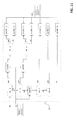
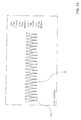
- the logic combination function LCF sets the voltage level of the measurement signal SDC according to the following look-up table (implemented by the exemplary flowchart of figure 11 ): Voltage level of the signal R1 Voltage level of the signal R2 Voltage level of the signal SDC low low intermediate high low high intermediate low high low high low high intermediate intermediate high low low intermediate low high intermediate intermediate intermediate intermediate
- the voltage level of the measurement signal SDC is set at a high level (e.g. 3.3V), it means that the time-invariant component of the differential current ID flows according to a first direction that may correspond to positive sign according to a given sign convention.
- the voltage level of the measurement signal SDC is set at a low level (e.g. - 3.3V)
- a low level e.g. - 3.3V
- the voltage level of the measurement signal SDC is set at an intermediate level (e.g. 0V), it means that the direction of the time-invariant component of the differential current ID cannot be determined (e.g. due to the fact that the time-invariant component of the differential current ID is null).
- the signal processing module 62 may be configured to set the voltage level of the measurement signal SDC according to the flowchart of figure 11 , which is a possible implementation of the look-up table shown above.
- the signal processing means 6 are preferably implemented in a digital manner.
- the second signal processing means 6 preferably comprise sampling means 63, which are preferably arranged to perform a digital sampling and a smooth filtering of the signals S1, S2 before further processing these latter.
- the sixth signals processing means 7 may be of known type.
- circuit configurations used in traditional ELCDs of the B-type may be adopted.
- the signal processing means 7 are implemented in analog manner, as described above.
- sampling means (not shown), which are preferably arranged to perform a digital sampling and a smooth filtering of the signal V1 before further processing this latter.
- the seventh signal processing means 8 comprise a tenth processing module 81 configured to process the fifth signal VD2 by means a second transformation function TF2.
- the signal processing module 81 advantageously provides the third measurement signal IDM.
- the transformation function TF2 allows calculating the values of the measurement signal IDM as a function of the values of the signal VD2.
- the transformation function TF2 may be a look-up table that allows associating a single value of the measurement signal IDM to a unique value of the signal VD2.
- the transformation function TF2 basically depends on the physical characteristics of the current transformer 21 and of the electronic implementation of the signal processing means 7. Advantageously, it may be experimentally set depending on the operating condition of the electronic device 1.
- the signal processing means 8 are preferably implemented in a digital manner.
- the second signal processing means 8 preferably comprise also sampling means 83, which are preferably arranged to perform a digital sampling and a smooth filtering of the signal VD2 before further processing this latter.
- the eighth signal processing means 9 may comprise an eleventh processing module 91 configured to process the third signal VD3 by means a third transformation function TF3.
- the signal processing module 91 advantageously provides the third measurement signal IDM.
- the transformation function TF3 allows calculating the values of the measurement signal IDM as a function of the values of the signal VD3.
- the transformation function TF3 may be a look-up table that allows associating a single value of the measurement signal IDM to a unique value of the signal VD3.
- the transformation function TF3 basically depends on the physical characteristics of the current transformer 21 and of the electronic implementation of the signal processing means 3. Advantageously, it may be experimentally set depending on the operating condition of the electronic device 1.
- the signal processing means 9 are preferably implemented in a digital manner.
- the second signal processing means 9 preferably comprise also sampling means 93, which are preferably arranged to perform a digital sampling and a smooth filtering of the signal VD3 before further processing this latter.
- the electronic device 1 preferably comprises fifth signal processing means 10 capable of providing the measurement signals IDC and possibly IAC and/or IDT.
- the signal processing means 10 are implemented in a digital manner.
- figure 18 it is shown an example of implementation of the electronic device 1, according to the invention, in an electronic arrangement 900 for LV or MV applications.
- the electronic device 1 is shown in the embodiment of figure 1 . However, also the embodiments shown in figures 1A , 1B may be adopted.
- the electronic arrangement 900 may be, for example, a battery charger for electric vehicles, a protection device or an IED (Intelligent Electronic Device) for LV or MV electric power distribution networks.
- IED Intelligent Electronic Device
- the measurement signals IDC and IAC and the trip signal TRIP provided by the electronic device 1 are acquired by a control unit 902 of the electronic arrangement 900.
- the control unit 902 may be advantageously configured to route the trip signal TRIP to activate a tripping unit 901 that is capable to interrupt the electric line 100.
- This solution is particularly useful in battery chargers and in protection devices for LV or MV electric power distribution networks.
- the control unit 902 may be advantageously configured to process the signals IDC, IAC to provide control signals C to implement advanced fault management functionalities.
- control unit 902 may be configured to process the signals IDC, IAC and generate suitable control signals C for a DC compensator (not shown), which may be advantageously provided with means for compensating the time-invariant component of a detected differential current ID.
- Said compensating means may, for example, be configured to inject in the electric line 100 a smooth DC current having an opposite sign of said time-invariant component, so to mitigate or remove the overall DC leakage.
- the electronic device 1 of the invention may be easily configured for applications different from the one shown in figure 18 .
- the electronic device 1 of the invention may also be configured for applications having different scale and current ratings from those mentioned above.
- the electronic device 1 of the invention has a number of advantages.
- the electronic device 1 is capable of detecting a differential current ID in an electric line 100 and providing quantitative information (including information regarding the sign) about the time-invariant and time-variant components of said differential current, which may be conveniently exploited according to the needs.
- the electronic device 1 is capable of providing accurate measurements of the time-invariant and time-variant components of a detected differential current.
- the electronic device 1 basically shows a substantially linear response (the measurement signals ICDM, IDM) to the measured quantity (the differential current ID) as it is possible to notice in graphs of figures 3 , 12 , 13 .
- time-invariant component of a differential current may be conveniently exploited to arrange compensation means capable of injecting in the electric line 100 an opposite time-invariant differential current.
- Such a compensation arrangement may ensure a longer operational service time of the electric line 100 or of the electrical systems/apparatuses connected thereto.
- a protection device arranged to trip the electric line 100 which incorporates the electronic device 1 and the mentioned compensation means, may be capable of remaining in a closed state for a longer time, thereby ensuring a prolonged service of the electric line without jeopardizing safety.
- Time-invariant component of a differential current may be conveniently exploited to improve functionalities of electrical apparatuses dedicated to LV or MV electric power distribution networks, such as protection devices, switching apparatuses, relays or the like.
- an ELCD Earth Leakage Current Device
- an ELCD Earth Leakage Current Device of the B-type incorporating the electronic device 1 can provide improved diagnostics functionalities, which may be suitably exploited to manage the operation of said protection device or for implementing advanced smart-grid management functionalities.
- information provided by the electronic device 1 may be easily communicated directly or through a proper communication network to any device of the electric power distribution network or of the control system in which the ELCD is installed.
- Information on the time-invariant component of a differential current may be conveniently exploited to verify, mitigate or correct maximal DC injection rates in an electric power distribution network by an electrical system, as prescribed by relevant standards for electric systems, including distributed resource interconnections with electric power systems and photovoltaic systems.
- the electronic device 1 can be easily embedded or integrated in many different LV or MV applications.
- the electronic device 1 can be easily used in:
- the adoption of the electronic device 1 in some applications may help to reduce overall installation costs of these latter.
- the installation on off-board charging equipment for vehicles in a domestic environment normally requires the substitution of the ECLDs of the domestic electric power distribution network.
- Such information may be used by a control unit of the charging equipment to interrupt the charging process when differential currents having non-negligible time-invariant components are present.
- the electronic device 1 may comprise autonomous processing resources (e.g. it may be provided with an own microcontroller) or it may share processing resources that are present in the device, apparatus or system, in which it is embedded or integrated.
- autonomous processing resources e.g. it may be provided with an own microcontroller
- processing resources may share processing resources that are present in the device, apparatus or system, in which it is embedded or integrated.
- the electronic device 1 may use a microcontroller (not shown) of the control unit 902 to execute software instructions for digitally implementing the functions of the processing means 4, 6, 8, 9, 10 described above.
- the electronic device 1 may also be used as stand-alone device and it can be easily put into communication with a remote device.
- the electronic device 1 is preferably provided with autonomous processing resources (e.g. a microcontroller).
- the electronic device 1 is easy and cheap to implement and/or manufacture at industrial level.
Landscapes
- Engineering & Computer Science (AREA)
- Power Engineering (AREA)
- Physics & Mathematics (AREA)
- General Physics & Mathematics (AREA)
- Measurement Of Current Or Voltage (AREA)
- Measuring Instrument Details And Bridges, And Automatic Balancing Devices (AREA)
Abstract
- a sensing circuit (2) comprising:
- a current transformer (21) having a magnetic core (211) through which the conductors of said electric line pass, a secondary winding (212) and an excitation winding (213) along which an excitation current (IE) circulates to polarize said magnetic core (211);
- an output circuit section (22) electrically connected to said secondary winding (212) and configured to provide a first signal (V1).
- first signal processing means (3) configured to process said first signal (V1) and provide a second signal (VD) indicative of said differential current (ID);
- second signal processing means (4) configured to process said second signal (VD) and provide a first measurement signal (IDCM) indicative of the absolute value of a time-invariant component of said differential current (ID);
- third signal processing means (5) configured to process said first signal (V1) and provide third and fourth signals (S1, S2) indicating whether said magnetic core (211) operates in a positive and/or in a negative saturation region of the hysteresis loop of said magnetic core;
- fourth signal processing means (6) configured to process said third and fourth signals (S1, S2) and provide a second measurement signal (SDC) indicative of the direction of the time-invariant component of said differential current (ID).
Description
- The present invention relates to an electronic device for measuring a differential current in an electric line.
- The electronic device of the invention is particularly suitable for low or medium voltage applications, where the term "low voltage" (LV) relates to voltages lower than 1 kV AC and 1.5 kV DC and the term "medium voltage" (MV) relates to voltages higher than 1 kV AC and 1.5 kV DC up to some tens of kV, e.g. up to 72 kV AC and 100 kV DC.
- As is known, in many LV or MV electric systems, e.g. in electric power distribution networks or photovoltaic electric power generation systems or battery charging systems for electric vehicles, it is necessary to detect possible differential currents among the conductors of an electric line.
- The presence of differential currents may, in fact, be indicative of occurring fault conditions. In the state of the art, many examples of protection devices are known, which are capable to detect the presence of AC or DC differential currents in an electric line.
- Many currently available solutions provide only qualitative information about a detected differential current. In practice, these devices are merely capable to indicate whether a detected differential current overcomes a given threshold value indicative of the presence of a fault condition.
- Other solutions are known, which are capable to provide also quantitative information about a detected differential current. Unfortunately, currently available devices of this type are often relatively complicated and expensive to manufacture at industrial level. In addition, they sometimes show poor performances in terms of a flexibility of use.
- The main aim of the present invention is to provide an electronic device for measuring a differential current in an electric line, which allows overcoming limitations of current solutions of the state of the art.
- Within this aim, an object of the present invention is to provide an electronic device that is capable of detecting a differential current in an electric line and providing quantitative information (measuring signals) about the detected differential current.
- A further object of the present invention is to provide an electronic device that offers outstanding performances in terms of flexibility of use.
- Yet another object of the present invention is to provide an electronic device that is relatively easy and cheap to manufacture at industrial level.
- The present invention thus provides an electronic device for measuring a differential current in an electric line, according to the following
claim 1 and the related dependent claims. - The electronic device, according to the invention, is capable of detecting and measuring a time-invariant component of a differential current among the conductors of an electric line, such as, for example, a leakage current caused by the deterioration of an electric insulation arrangement or by the failure of components connected to ground.
- In particular, the electronic device, according to the invention, is capable of providing information indicative of the absolute value and the flowing direction of a time-invariant component of a differential current among the conductors of an electric line.
- The electronic device, according to the invention, is also capable of detecting and measuring a time-variant component of a differential current among the conductors of an electric line, such as, for example, a ground fault current.
- For the sake of clarity, the terms "time-invariant component" and "time-variant component" of a differential current respectively mean a DC component and an AC component of said differential current.
- As is widely known, a differential current in an electric line may include only a DC current or only AC current or, more frequently, is the result of the superimposition of AC and DC currents.
- Currents varying much slowly with respect to the variation rates (e.g. 50Hz) commonly used in LV or MV electrical systems are here considered as DC currents.
- Currents not having a sine wave-form but showing periodic variations (e.g. pulsed currents, partialized currents or the like) are here considered as AC currents.
- The electronic device, according to the invention, is capable of detecting a differential current in an electric line, decomposing the detected differential current in its DC and AC components and providing measuring signals indicative of each of said components.
- The quantitative information about the time-invariant and time-variant components of a differential current in an electric line may be conveniently exploited in many kinds of LV and MV applications.
- As an example, in a battery charging system for vehicles, information collected by measuring the time-invariant component of a detected differential current may be used to compensate small intrinsic DC earth leakages occurring during normal operating conditions or to ensure a correct operation of protection devices positioned upstream with respect to the point of the installation at which said DC earth leakages occur.
- As a further example, in LV or MV electric power distribution networks, measurement information about the time-invariant and time variant components of a differential current may be used to practically implement advanced protection or fault-management strategies. Further aspects of the invention relate to an electronic arrangement for LV or MV applications, according to the following claims 13 and 14.
- A further aspect of the invention relates to a photovoltaic electric power generation system, according to the following claim 15.
- A further aspect of the invention relates to a LV or MV electric power distribution system or network, according to the following claim 16.
- Further characteristics and advantages of the invention will emerge from the description of preferred, but not exclusive, embodiments of the power and control unit for a low or medium voltage apparatus, according to the invention, non-limiting examples of which are provided in the attached drawings, wherein:
-
Figure 1 schematically shows an embodiment the electronic device, according to the invention; and -
Figure 1A schematically shows a further embodiment the electronic device, according to the invention; and -
Figure 1B schematically shows a further embodiment the electronic device, according to the invention; and -
Figures 2-13 schematically show different kinds of signal processing means included in the electronic device, according to the invention; and -
Figures 14-17 schematically show some possible waveforms of a signal in the electronic device, according to the invention; and -
Figure 18 schematically shows an electronic arrangement for LV or MV applications, which comprises the electronic device, according to the invention. - Referring to the cited figures, the present invention relates to an
electronic device 1 for measuring a differential current ID in a LV or MVelectric line 100. - The
electric line 100 may be, for example, an electric power supply line of an electric power distribution network or a battery charging system for electric vehicles. - The
electric line 100 comprises a plurality of conductors and it may be, for example, of the single or multi-phase type. - The
electronic device 1 comprises asensing circuit 2 operatively coupled to the conductors of theelectric line 100. - Referring to
figure 2 , thesensing circuit 2 advantageously comprises acurrent transformer 21 provided with amagnetic core 211, preferably shaped as a toroid. - Advantageously, the
magnetic core 211 has a high magnetic permeability and it may be made, for example, of a Ni-Fe alloy. - The
transformer 21 is advantageously arranged to sense unbalancing currents among the conductors of theelectric line 100. - The conductors of the
electric line 100 pass through themagnetic core 211 so as to form the primary winding for thetransformer 21. - In order to increase the overall sensitivity to possible differential currents in the
electric line 100, the conductors of theprimary line 100 may be wound around themagnetic core 211 to form multiple turns, for example 3 turns. - The
transformer 21 has asecondary winding 212 that is advantageously wound around themagnetic core 211 with a relatively high number of turns, for example 250 turns. - The
transformer 21 further comprises an excitation winding 213, which is advantageously wound around themagnetic core 211 with a relatively high number of turns, for example 250 turns. - During the operation of the
electronic device 1, an AC excitation current IE circulates along the excitation winding 213. - The excitation current IE may be advantageously generated by a
generation circuit 214 that may be of the known type, for example an electronic oscillator circuit. - As an example, the excitation current IE may have a frequency of 500 Hz and a waveform that may be, for example, sinusoidal.
- As it occurs in other known LV-MV applications, for example in a traditional ELCD (Earth Leakage Current Device) of the B-type, the excitation current IE polarizes the
magnetic core 211 of thetransformer 21 at an operating point in which the magnetic permeability of themagnetic core 211 shows a strong transition towards small values, namely at an operating point located close a positive or negative saturation region of the hysteresis loop of themagnetic core 211. - The
sensing circuit 2 comprises anoutput circuit section 22 electrically connected to thesecondary winding 212 of thetransformer 21. - The
output circuit section 22 is configured to provide a first signal V1 (preferably a voltage signal) indicative of the differential current ID. Basically, it receives a current circulating along thesecondary winding 212 and generates the signal V1. - The
output circuit section 22 may advantageously comprise a resistive circuit (e.g. a shunt-resistor connected between a terminal of the secondary winding and ground) to generate the signal V1. -
Figures 14-17 show some experimental measurements of the signal V1 in different operative conditions. - The signal V1 is basically an AC signal comprising a fixed AC signal component FSC due to circulation of the excitation current IE along the excitation winding 213.
- When no differential current ID is present among the conductors of the
electric line 100, the signal V1 basically depends on the waveform and carrier frequency of the excitation current IE only (figure 14 ). - When it is present a differential current ID having only a time-invariant component, the signal V1 has the same frequency of the excitation current IE but it may show first amplitude over-shoots OS1 occurring with multiple frequencies of the excitation current IE (
figure 15 ). The amplitude over-shoots OS1 may be positive or negative depending on the direction of the current ID. - When it is present a differential current ID having only a time-variant component, the signal V1 has the same carrier frequency of the excitation current IE but it may show a waveform modulated in amplitude and second amplitude over-shoots OS2 occurring with frequencies different from the frequency of the excitation current IE (
figure 16 ). The amplitude over-shoots OS2 may be positive and/or negative. - When it is present a differential current ID having both time-invariant and time-variant components, the voltage V1 has the same carrier frequency of the excitation current IE but it may show a waveform possibly modulated in amplitude and having amplitude overshoots induced by the nonlinear, saturating behaviour of the magnetic material of the
magnetic core 211. - For example, as shown in
figure 17 , the waveform may have the first and second amplitude overshoots OS1, OS2 described above. The waveform may have higher and lower amplitude over-shoots OS2 (positive and/or negative) occurring with frequencies different from the frequency of the excitation current IE. - Referring now to
figures 1 ,1A ,1B , according to the invention, theelectronic device 1 comprises first signal processing means 3 configured to process the signal V1. The signal processing means 3 provide a second signal VD (preferably a voltage signal) indicative of a differential current ID detected by thesensing circuit 2. - When no differential current ID is present among the conductors of the
electric line 100, the signal VD has amplitude substantially null (e.g. 0.4V). - When a differential current ID is present, the signal VD is substantially a function of the time-invariant and time-variant components of the differential current ID.
- Preferably, the signal processing means 3 are configured so that they provide a signal VD that is more sensitive to the time-invariant component of the differential current ID.
- The
electronic device 1 comprises second signal processing means 4 configured to process the second signal VD. - The second signal processing means 4 provide a first measurement signal IDCM indicative of the absolute value of a time-invariant component of a differential current ID detected by the
sensing circuit 2. - The signal processing means 4 calculate the measurement signal IDCM substantially according to the mathematical relation IDCM=f(VD) +Err, where Err is a measurement error (due to the time-variant component of the differential current ID along with other possible, minor, affecting factors not relevant to the invention).
- On the field measurements have shown that the measurement error Err is relatively small for most of the applications in which the
electronic device 1 may be adopted. The measurement error Err can thus be neglected without prejudice for the overall reliability of theelectronic device 1. - The
electronic device 1 comprises third signal processing means 5 configured to process the signal V1. - The signal processing means 5 provide third and fourth signals S1, S2 (preferably voltage signals) that indicate whether the
magnetic core 211 of thetransformer 21 operates in a positive or in a negative saturation region of its own hysteresis loop, when the differential current ID has a time-invariant current component that is not null. - The signal processing means 5 are advantageously configured to provide information on the non-linear effect produced on the
magnetic core 211 by said time-invariant component. - In the
magnetic core 211, a magnetic field is present due to the superimposition of a magnetic field generated by the excitation current IE and a magnetic field generated by the differential current ID. - Such a magnetic field may be prevalently positive or negative depending on whether the time-invariant component of the differential current ID is respectively positive or negative (according to a given sign convention).
- Signals S1, S2 are indicative of such a non-linear behaviour of the
magnetic core 211 and thus can be used to obtain information on the flowing direction (sign) of the time-invariant component of a differential current ID among the conductors of theelectric line 100. - The
electronic device 1 comprises fourth signal processing means 6 configured to process the third and fourth signals S1, S2. - The signal processing means 6 provide a second measurement signal SDC indicative of the direction of the time-invariant component of a differential current ID detected by the
sensing circuit 2. - As illustrated above, a prevalently positive or negative magnetic field may be present in the
magnetic core 211 of thetransformer 21, when a differential current ID is present among the conductors of theelectric line 100. - The non-linear effect produced on the
magnetic core 211 by the time-invariant component of the differential current ID may be high, moderate or low. - The signal processing means 6 process the signals S1, S2 to provide information R1, R2 indicating whether the intensity of the signals S1, S2 is at a high, moderate or low level (
figures 11-12 ). - Then, the signal processing means 6 process such information R1, R2 to determine the sign of the time-invariant component of the differential current ID.
- As it will be explained in more details in the following, in some cases the sign of the time-invariant component of the differential current ID cannot be determined because the non-linear effect produced on the
magnetic core 211 is null or too moderate. - According to an aspect of the invention, the
electronic device 1 may comprise fifth signal processing means 10 configured to process the measurement signals IDCM and SDC and provide a fourth measurement signal IDC indicative of the time-invariant component (with its sign) of a detected differential current ID. - The quantitative information IDC may be calculated on the base of measurement data IDCM, SDC. To this aim, the processing means 10 may be configured to calculate the data IDC on the base of the following mathematical relation: IDC = SDC * IDCM.
- According to an aspect of the invention, the
electronic device 1 is also capable of providing quantitative information IAC about the time-variant component of a detected differential current ID. - In a possible embodiment of the invention (
figures 1 ,18 ), theelectronic device 1 comprises sixth signal processing means 7 configured to process the first signal V1 and provide a fifth signal VD2 (preferably a voltage signal) indicative of the differential current ID. - When a differential current ID is present, the signal VD2 is substantially a function of the time-invariant and time-variant components of the differential current ID.
- Preferably, the signal processing means 7 are configured so that they provide a signal VD2 that is more sensitive to the time-variant component of the differential current ID.
- The
electronic device 1 comprises seventh signal processing means 8 configured to process the fifth signal VD2 and provide a third measurement signal IDM indicative of the absolute value of the differential current ID. - In an alternative embodiment of the invention (
figure 1A ), the signal processing means 3 are advantageously configured to provide a sixth signal VD3 (preferably a voltage signal) indicative of the differential current ID. - In some embodiments, the sixth signal VD3 may coincide with the second signal VD.
- The
electronic device 1 comprises eighth signal processing means 9 configured to process the signal VD3 and provide the third measurement signal IDM. - Preferably, the fifth signal processing means 10 are also configured to process the measurement signals IDCM, IDM and provide a fifth measurement signal IAC indicative of the time-variant component of the differential current ID.
- The quantitative information IAC may be complementary calculated on the base of measurement data IDCM, IDM.
- According to an aspect of the invention, the
electronic device 1 is also capable of providing quantitative information IDT about a detected differential current ID. - In this case, the signal processing means 10 are also configured to process the measurement signals IDCM, SDC, IDM and provide a sixth measurement signal IDT indicative of the overall differential current ID present between the conductors of the
electric line 100. - Other solutions for additionally providing the measurement signals IAC and/or IDT are possible.
- For example, in a further embodiment of the invention (
figure 1B ), which is particularly suitable for a digital implementation, the processing means 10 may be configured to process the measurement signals IDCM, SDC and the signal V1 in order to provide the measurement signal IAC and/or the measurement signal IDT. - The signal processing means 3, 4, 5, 6, 7, 8, 9, 10 may be industrially implemented in an analog and/or digital manner.
- If they are implemented in analog manner, they comprise electronic circuits suitably arranged to perform the functions of said processing means. Said electronic circuits may form separated circuit units or may be at least partially integrated in one or more circuit units.
- If they are implemented in a digital manner, they comprise suitably arranged software instructions stored in a medium and executable by one or more computerised units (e.g. microprocessors) to perform the functions of said processing means.
- The present invention will be now described in more details with reference to embodiments, in which the signal processing means 3, 5, 7 are implemented in an analog manner and the processing means 4, 6, 8, 9, 10 are implemented in a digital manner.
- This choice is not intended to limit the scope of the invention in any way.
- Other embodiments, in which one or more of the signal processing means 3, 5, 7 are implemented in a digital manner and in which one or more of the signals processing means 4, 6, 8, 9, 10 are implemented in an analog manner, are possible and fall within the scope of the present invention.
- Referring to
figures 3-4 , according to an aspect of the invention, the first signal processing means 3 preferably comprise a firstsignal processing module 31 configured to perform an amplitude filtering of the signal V1. - The
signal processing module 31 provides in output a first intermediate signal VI1 (preferably a voltage signal), which is a function of the time-invariant and time-variant components of a differential current ID circulating among the conductors of theelectric line 100. - The
signal processing module 31 is advantageously configured to cut-off the fixed AC signal component FSC that is due to the circulation of the excitation current IE along the excitation winding 213. - Preferably, the first
signal processing module 31 comprises adiode bridge circuit 311 and a cascade of amplifyingcircuits diode bridge circuit 311. Preferably, the amplifyingcircuit 312 comprises anoperation amplifier 3120 arranged in a known manner to provide amplification functionalities. As an example, theoperational amplifier 3120 may be electrically connected to aresistive network 3121 and a resistive-capacitive network 3122. - Similarly, the amplifying
circuit 313 may comprise anoperation amplifier 3130 that may be arranged in a known manner to provide amplification functionalities. As an example, theoperational amplifier 3130 may be electrically connected to aresistive network 3131 and a resistive-capacitive network 3132. - Other solutions are possible, in which a sole amplifying circuit is adopted in substitution of the amplifying circuits 312-313.
- Preferably, the
signal processing module 31 comprises an output filtering circuit 314 (e.g. of capacitive type in a known configuration) to filter undesired frequency components of the signal VI1. - Preferably, the
diode bridge circuit 311, the amplifyingcircuit 312, the amplifyingcircuit 313 and theoutput filtering circuit 314 are electrically connected in series according to the configuration shown infigure 4 . - Other circuit configurations are possible. As an example, the position of the
diode bridge circuit 311 and of the amplifyingcircuits - Referring to
figures 3 and5-6 , the first signal processing means 3 preferably comprise a secondsignal processing module 32 configured to perform a wave-form rectification of the signal VI1 provided in output by thesignal processing module 31. - The
signal processing module 32 provides a second intermediate signal VI2 (preferably a voltage signal), which is a rectified signal. - The second
signal processing module 32 may comprise anoperation amplifier 320 arranged in a known manner to provide rectification functionalities. As an example, theoperational amplifier 320 may be suitably electrically connected to theresistive networks diode network 323. Theresistive network 321 may be of known type whereas theresistive network 322 is preferably a bridge of resistors having suitable resistance values. - Preferably, the first signal processing means 3 comprise a third
signal processing module 33 configured to perform a low-pass filtering of the signal VI2 provided in output by the secondsignal processing module 32. Thesignal processing module 33 provides in output the second signal VD. - Preferably, the
signal processing module 33 comprises anintegrator circuit 331 that is electrically connected to a voltage-follower circuit 332. - The
integrator circuit 331 may comprise anoperation amplifier 3310 arranged in a known manner to provide integration functionalities. As an example, theoperational amplifier 3310 may be electrically connected to resistive-capacitive networks - The voltage-
follower circuit 332 may also comprise anoperation amplifier 3320 arranged in a known manner to provide voltage-follower functionalities. - It is again evidenced that the processing means 3 (in particular the processing module 31) are configured to cut-off the AC signal component FSC due to the circulation of the excitation current IE.
- The signals VI1, VI2 and VD therefore provide information on the absolute value of the differential current ID only.
- When no differential current ID is present among the conductors of the
electric line 100, the signals VI1, VI2 and VD have amplitude substantially null (e.g. at 0.4V). - When a differential current ID is present, the signals VI1, VI2 and VD have an amplitude not null at the instants (
figures 12-15 ) in which the first signal V1 exceeds the amplitude of the fixed AC signal component FSC that is due to the presence of the excitation current IE (e.g. at the amplitude overshoots OS1, OS2). - The
signal processing modules - However, they may be also implemented in a digital manner. In this case, the
signal processing module 31 may advantageously comprise sampling means (not shown), which are preferably arranged to perform a digital sampling and a smooth filtering of the signal V1 before further processing this latter. - Referring to
figure 3 , according to an aspect of the invention, the second signal processing means 4 preferably comprise afourth processing module 41 configured to process the second signal VD by means a first transformation function TF. - The
signal processing module 41 advantageously provides the first measurement signal IDCM. - The transformation function TF allows calculating the values of the measurement signal IDCM as a function of the values of the signal VD.
- As example, the transformation function TF may be a look-up table that allows associating a single value of the measurement signal IDCM to a unique value of the signal VD.
- The transformation function TF basically depends on the physical characteristics of the
current transformer 21 and of the electronic implementation of the signal processing means 3. Advantageously, it may be experimentally set depending on the operating condition of theelectronic device 1. - According to an aspect of the invention, the signal processing means 4 may comprise a fifth
signal processing module 42 configured to compare the signal VD with a threshold value VTH (preferably a voltage value). - The
signal processing module 42 provides a trip signal TRIP that depends on the behaviour of the signal VD. - As an example, the trip signal TRIP may be a logic signal that is set at a tripping command level (e.g. a high level of 3.3V), when the signal VD exceeds the threshold value or signal VTH.
- The threshold value VTH may be set according to the application, in which the
electronic device 1 is adopted. - As an example, when the
electronic device 1 is used in a battery charger for electric vehicles, the threshold value VTH may be 2V. - The signal processing means 4 are preferably implemented in a digital manner.
- In this case, when the signal processing means 3 are implemented in an analog manner, the second signal processing means 4 preferably comprise also sampling means 43, which are preferably arranged to perform a digital sampling and a smooth filtering of the signal VD before further processing this latter.
- Referring to
figures 7-8 , according to an aspect of the invention, the third signal processing means 5 preferably comprise a sixthsignal processing module 51 configured to compare the first signal V1 with a first reference signal VR1 and with a second reference signal VR2 having opposite sign. As an example, the reference signals VR1, VR2 are reference voltages that may be positive and negative, respectively. - The
signal processing module 51 provides a first comparison signal VC1 (preferably a voltage signal) and a second comparison signal VC2 (preferably a voltage signal). - The
signal processing module 51 preferably comprisesoperation amplifiers - The signal processing means 5 preferably comprise a seventh
signal processing module 52 configured to perform a low-pass filtering of the comparison signals VC1, VC2. - The
signal processing module 52 provides the third and fourth signals S1, S2. - The
signal processing module 52 may comprise filteringcircuits operational amplifiers - Preferably, the signals S1, S2 are two-level signals that are functions of the signal V1. Preferably, the signals S1, S2 have the behaviour shown in
figure 7 . - The signal S1 is at a high level (e.g. 3.3V) when the signal V1 is higher than a positive threshold value (the reference value VR1) whereas it is at a low level (e.g. 0V) when the signal V1 is lower than the reference value VR1.
- The signal S2 is at a high level when the signal V1 is lower than a negative threshold value (the reference value VR2) whereas it is at a low level when the signal V1 is higher than the reference voltage VR2.
- The reference voltages VR1, VR2 may be set according to the application in which the electronic device is adopted. As an example, when the
electronic device 1 is used in a charging system for electric vehicles the reference voltages VR1, VR2 may be set at 1V and - 1V, respectively. - The
signal processing modules - However, they may be easily implemented in a digital manner, too. In this case, the
signal processing module 51 may advantageously comprise sampling means (not shown), which are preferably arranged to perform a digital sampling and a smooth filtering of the signal V1 before further processing this latter. - Referring to
figures 9-11 , according to an aspect of the invention, the fourth signal processing means 6 preferably comprise an eighthsignal processing module 61 configured to process the signals S1, S2 according to at least one threshold filtering function TFF. - The
signal processing module 61 provides fifth and sixth signals R1, R2 (preferably voltage signals) indicative of the intensity of the signals S1, S2. - Preferably, the threshold filtering function TFF provides three-level signals R1, R2 that are functions of the signals S1, S2, respectively.
- Preferably, the signals R1, R2 have the behaviour shown in
figure 10 . - From a data processing point of view, the
signal processing module 61 may be configured to set the level of the signals R1, R2 according to the flowchart offigure 10 , which is a possible implementation of the threshold filtering function TFF. - The
signal processing module 61 compares each signals S1, S2 with a lower threshold value STH1 (preferably a voltage value) and a higher threshold value STH2 (preferably a voltage value), which advantageously are both positive. Based on the result of said comparison, thesignal processing module 61 provides a corresponding signal R1, R2 at a given level. - For each signal R1, R2, the
signal processing module 61 selects a voltage level that is indicative of the intensity (low, moderate, high) of the corresponding signal S1, S2. This latter is, in turn, indicative of the non-linear effects produced on themagnetic core 211 of thetransformer 21 by the time-invariant component of the differential current ID. - If the signal S1, S2 is lower than the lower threshold value STH1, the
signal processing module 61 provides a corresponding signal R1, R2 at a low level (e.g. 0V). - If the signal S1, S2 is comprised between the threshold values STH1 and STH2, the
signal processing module 61 provides a corresponding signal R1, R2 at an intermediate level (e.g. 2.5V). - If the signal S1, S2 is higher than the higher threshold value STH2, the
signal processing module 61 provides a corresponding signal R1, R2 at a high level (e.g. 3.3V). - The threshold values STH1, STH2 may be set according to the application in which the electronic device is adopted. As an example, when the
electronic device 1 is used in a charging system for electric vehicles the threshold values STH1, STH2 may be set at 1.1V and 2.2V, respectively. - The signal processing means 6 preferably comprise a ninth
signal processing module 62 configured to process the signals R1, R2 according to at least a logic combination function - LCF.
- The
signal processing module 62 provides the second measurement signal SDC. - Preferably, the measurement signal SDC may have three voltage levels, similarly to the signals R1, R2.
- The voltage level of the measurement signal SDC is set depending on the levels of the signals R1, R2.
- Preferably, the logic combination function LCF sets the voltage level of the measurement signal SDC according to the following look-up table (implemented by the exemplary flowchart of
figure 11 ):Voltage level of the signal R1 Voltage level of the signal R2 Voltage level of the signal SDC low low intermediate high low high intermediate low high low high low high high intermediate intermediate high low low intermediate low high intermediate high intermediate intermediate intermediate - If the voltage level of the measurement signal SDC is set at a high level (e.g. 3.3V), it means that the time-invariant component of the differential current ID flows according to a first direction that may correspond to positive sign according to a given sign convention.
- If the voltage level of the measurement signal SDC is set at a low level (e.g. - 3.3V), it means that the time-invariant component of the differential current ID flows according to a second direction that is opposite to the first direction and that may correspond to negative sign according to the said given sign convention.
- If the voltage level of the measurement signal SDC is set at an intermediate level (e.g. 0V), it means that the direction of the time-invariant component of the differential current ID cannot be determined (e.g. due to the fact that the time-invariant component of the differential current ID is null).
- From a physical point of view, the adoption of the look-up table shown above is justified by the following facts:
- if the time-invariant component of the differential current ID is positive (or negative) according to a given sign convention, it induces a non-linear behaviour of the
magnetic core 211 of thetransformer 21 that is of the same sign. Such a non-linear effect may be moderate or high; - if the time-invariant component of the differential current ID is null or negligible, it induces a non-linear behaviour of the
magnetic core 211 of thetransformer 21 that is low or moderate. - From a data processing point of view, the
signal processing module 62 may be configured to set the voltage level of the measurement signal SDC according to the flowchart offigure 11 , which is a possible implementation of the look-up table shown above. - The signal processing means 6 are preferably implemented in a digital manner.
- In this case, when the signal processing means 5 are implemented in an analog manner, the second signal processing means 6 preferably comprise sampling means 63, which are preferably arranged to perform a digital sampling and a smooth filtering of the signals S1, S2 before further processing these latter.
- Referring now to
figure 12 , which refers to the embodiment shown infigure 1 , the sixth signals processing means 7 may be of known type. - As an example, circuit configurations used in traditional ELCDs of the B-type may be adopted.
- Preferably, the signal processing means 7 are implemented in analog manner, as described above.
- However, they may be easily implemented in a digital manner, too. In this case, they may advantageously comprise sampling means (not shown), which are preferably arranged to perform a digital sampling and a smooth filtering of the signal V1 before further processing this latter.
- Preferably, the seventh signal processing means 8 comprise a
tenth processing module 81 configured to process the fifth signal VD2 by means a second transformation function TF2. Thesignal processing module 81 advantageously provides the third measurement signal IDM. The transformation function TF2 allows calculating the values of the measurement signal IDM as a function of the values of the signal VD2. - As example, the transformation function TF2 may be a look-up table that allows associating a single value of the measurement signal IDM to a unique value of the signal VD2.
- The transformation function TF2 basically depends on the physical characteristics of the
current transformer 21 and of the electronic implementation of the signal processing means 7. Advantageously, it may be experimentally set depending on the operating condition of theelectronic device 1. - The signal processing means 8 are preferably implemented in a digital manner.
- When the signal processing means 7 are implemented in an analog manner, the second signal processing means 8 preferably comprise also sampling means 83, which are preferably arranged to perform a digital sampling and a smooth filtering of the signal VD2 before further processing this latter.
- Referring now to
figure 13 , which refers to the embodiment shown infigure 1A , the eighth signal processing means 9 may comprise aneleventh processing module 91 configured to process the third signal VD3 by means a third transformation function TF3. - The
signal processing module 91 advantageously provides the third measurement signal IDM. The transformation function TF3 allows calculating the values of the measurement signal IDM as a function of the values of the signal VD3. - As example, the transformation function TF3 may be a look-up table that allows associating a single value of the measurement signal IDM to a unique value of the signal VD3.
- The transformation function TF3 basically depends on the physical characteristics of the
current transformer 21 and of the electronic implementation of the signal processing means 3. Advantageously, it may be experimentally set depending on the operating condition of theelectronic device 1. - The signal processing means 9 are preferably implemented in a digital manner.
- When the signal processing means 3 are implemented in an analog manner, the second signal processing means 9 preferably comprise also sampling means 93, which are preferably arranged to perform a digital sampling and a smooth filtering of the signal VD3 before further processing this latter.
- As mentioned above, the
electronic device 1 preferably comprises fifth signal processing means 10 capable of providing the measurement signals IDC and possibly IAC and/or IDT. Preferably, the signal processing means 10 are implemented in a digital manner. - In
figure 18 , it is shown an example of implementation of theelectronic device 1, according to the invention, in anelectronic arrangement 900 for LV or MV applications. - The
electronic device 1 is shown in the embodiment offigure 1 . However, also the embodiments shown infigures 1A ,1B may be adopted. - The
electronic arrangement 900 may be, for example, a battery charger for electric vehicles, a protection device or an IED (Intelligent Electronic Device) for LV or MV electric power distribution networks. - The measurement signals IDC and IAC and the trip signal TRIP provided by the
electronic device 1 are acquired by acontrol unit 902 of theelectronic arrangement 900. - The
control unit 902 may be advantageously configured to route the trip signal TRIP to activate a trippingunit 901 that is capable to interrupt theelectric line 100. - This solution is particularly useful in battery chargers and in protection devices for LV or MV electric power distribution networks.
- The
control unit 902 may be advantageously configured to process the signals IDC, IAC to provide control signals C to implement advanced fault management functionalities. - As an example, in a battery charger, the
control unit 902 may be configured to process the signals IDC, IAC and generate suitable control signals C for a DC compensator (not shown), which may be advantageously provided with means for compensating the time-invariant component of a detected differential current ID. - Said compensating means may, for example, be configured to inject in the electric line 100 a smooth DC current having an opposite sign of said time-invariant component, so to mitigate or remove the overall DC leakage.
- Those skilled in the art may easily understand that the
electronic device 1 of the invention may be easily configured for applications different from the one shown infigure 18 . - The
electronic device 1 of the invention may also be configured for applications having different scale and current ratings from those mentioned above. - The
electronic device 1 of the invention has a number of advantages. - The
electronic device 1 is capable of detecting a differential current ID in anelectric line 100 and providing quantitative information (including information regarding the sign) about the time-invariant and time-variant components of said differential current, which may be conveniently exploited according to the needs. - The
electronic device 1 is capable of providing accurate measurements of the time-invariant and time-variant components of a detected differential current. In fact, theelectronic device 1 basically shows a substantially linear response (the measurement signals ICDM, IDM) to the measured quantity (the differential current ID) as it is possible to notice in graphs offigures 3 ,12 ,13 . - Information on the time-invariant component of a differential current may be conveniently exploited to arrange compensation means capable of injecting in the
electric line 100 an opposite time-invariant differential current. - Such a compensation arrangement may ensure a longer operational service time of the
electric line 100 or of the electrical systems/apparatuses connected thereto. - As an example, a protection device arranged to trip the
electric line 100, which incorporates theelectronic device 1 and the mentioned compensation means, may be capable of remaining in a closed state for a longer time, thereby ensuring a prolonged service of the electric line without jeopardizing safety. - Information on the time-invariant component of a differential current may be conveniently exploited to improve functionalities of electrical apparatuses dedicated to LV or MV electric power distribution networks, such as protection devices, switching apparatuses, relays or the like.
- As an example, an ELCD (Earth Leakage Current Device) of the B-type incorporating the
electronic device 1 can provide improved diagnostics functionalities, which may be suitably exploited to manage the operation of said protection device or for implementing advanced smart-grid management functionalities. In this last case, information provided by theelectronic device 1 may be easily communicated directly or through a proper communication network to any device of the electric power distribution network or of the control system in which the ELCD is installed. - Information on the time-invariant component of a differential current may be conveniently exploited to verify, mitigate or correct maximal DC injection rates in an electric power distribution network by an electrical system, as prescribed by relevant standards for electric systems, including distributed resource interconnections with electric power systems and photovoltaic systems.
- The
electronic device 1 can be easily embedded or integrated in many different LV or MV applications. - For instance, the
electronic device 1 can be easily used in: - on-board battery chargers, off-board charging equipment, in-cable portable charging equipment, vehicle power supply equipment for vehicles; and/or
- residual current devices, tripping devices, protection devices, switching apparatuses, relays and control devices for electric power distribution networks; and/or
- IEDs, i.e. electronic microcontroller-based devices for managing operation of electric power equipment for electric power distribution networks;
- photovoltaic electric power generation systems.
- The adoption of the
electronic device 1 in some applications may help to reduce overall installation costs of these latter. - As an example, the installation on off-board charging equipment for vehicles in a domestic environment normally requires the substitution of the ECLDs of the domestic electric power distribution network.
- These latter devices, in fact, are traditionally of A and AC type and are subject to malfunctioning in presence of possible differential currents having non-negligible time-invariant components during the battery charging process.
- By adopting the
electronic device 1, it is possible to perform precise measurements of the time-invariant component of possible differential currents and check whether said time-invariant component exceeds a given threshold value (e.g. 6 mA). - Such information may be used by a control unit of the charging equipment to interrupt the charging process when differential currents having non-negligible time-invariant components are present.
- Protection functionalities of the ECLDs of the domestic electric power distribution network are thus ensured without the need of expensive substitution interventions.
- The
electronic device 1 may comprise autonomous processing resources (e.g. it may be provided with an own microcontroller) or it may share processing resources that are present in the device, apparatus or system, in which it is embedded or integrated. - As an example, referring to
figure 18 , theelectronic device 1 may use a microcontroller (not shown) of thecontrol unit 902 to execute software instructions for digitally implementing the functions of the processing means 4, 6, 8, 9, 10 described above. - The
electronic device 1 may also be used as stand-alone device and it can be easily put into communication with a remote device. In this case, theelectronic device 1 is preferably provided with autonomous processing resources (e.g. a microcontroller). - The
electronic device 1 is easy and cheap to implement and/or manufacture at industrial level.
Claims (16)
- An electronic device (1) for measuring a differential current (ID) in an electric line (100) having a plurality of conductors, said electronic device comprising:- a sensing circuit (2) comprising:characterised in that it comprises:- a current transformer (21) having a magnetic core (211) operatively coupled to the conductors of said electric line, a secondary winding (212) and an excitation winding (213) along which an excitation current (IE) circulates to polarize said magnetic core (211);- an output circuit section (22) electrically connected to said secondary winding (212) and configured to provide a first signal (V1) indicative of said differential current;- first signal processing means (3) configured to process said first signal (V1) and provide a second signal (VD) indicative of said differential current (ID);- second signal processing means (4) configured to process said second signal (VD) and provide a first measurement signal (IDCM) indicative of the absolute value of a time-invariant component of said differential current (ID);- third signal processing means (5) configured to process said first signal (V1) and provide third and fourth signals (S1, S2) indicative of whether said magnetic core (211) operates in a positive or in a negative saturation region of the hysteresis loop of said magnetic core;- fourth signal processing means (6) configured to process said third and fourth signals (S1, S2) and provide a second measurement signal (SDC) indicative of the direction of the time-invariant component of said differential current (ID).
- An electronic device, according to claim 1, characterised in that it comprises fifth signal processing means (10) configured to process said first and second measurement signals (IDCM, SDC) and provide a fourth measurement signals (IDC) indicative of the time-invariant component of said differential current (ID).
- An electronic device, according to claims 1 or 2, characterised in that it comprises:- sixth signal processing means (7) configured to process said first signal (V1) and provide a fifth signal (VD2) indicative of said differential current (ID);- seventh signal processing means (8) configured to process said fifth signal (VD2) and provide a third measurement signal (IDM) indicative of the absolute value of said differential current (ID).
- An electronic device, according to claims 1 or 2, characterised in that said first signal processing means (3) are configured to provide a sixth signal (VD3) indicative of said differential current, said electronic device comprising eighth signal processing means (9) configured to process said sixth signal (VD3) and provide a third measurement signal (IDM) indicative of the absolute value of said differential current (ID).
- An electronic device, according to claims 2 and 3 or according to claims 2 and 4, characterised in that said fifth signal processing means (10) are also configured to process said first and third measurement signals (IDCM, IDM) and provide a fifth measurement signal (IAC) indicative of the time-variant components of said differential current (ID).
- An electronic device, according to claims 2, 3 and 5 or according to claims 2, 4 and 5 characterised in that said fifth signal processing means (10) are also configured to process said first, second and third measurement signals (IDCM, SDC, IDM) and provide a sixth measurement signal (IDT) indicative of said differential current (ID).
- An electronic device, according to claim 2, characterised in that said fifth signal processing means (10) are also configured to process said first and second measurement signals (IDCM, SDC) and said first signal (V1) and provide a fifth measurement signal (IAC) indicative of the time-variant components of said differential current (ID) and/or sixth measurement signal (IDT) indicative of said differential current (ID).
- An electronic device, according to one or more of the previous claims, characterised in that said first signal processing means (3) comprise:- a first signal processing module (31) configured to perform an amplification and an amplitude filtering of said first signal (V1), said first signal processing module providing a first intermediate signal (VI1) that is indicative of said differential current (ID);- a second signal processing module (32) configured to perform a wave-form rectification of said first intermediate signal (VI1), said second signal processing module providing a second intermediate signal (VI2);- a third signal processing module (33) configured to perform a low-pass filtering of said second intermediate signal (VI2), said third signal processing module providing said second signal (VD).
- An electronic device, according to one or more of the previous claims, characterised in that said second signal processing means (4) comprise a fourth processing module (41) configured to process said second signal (VD) by means a first transformation function (TF), said fourth signal processing module providing said first measurement signal (IDCM).
- An electronic device, according to one or more of the previous claims, characterised in that said second signal processing means (4) comprise a fifth signal processing module (42) configured to compare said second signal (VD) with a threshold value (VTH) and provide a trip signal (TRIP) depending on the behaviour of said second signal (VD).
- An electronic device, according to one or more of the previous claims, characterised in that said third signal processing means (5) comprise:- a sixth signal processing module (51) configured to compare said first signal (V1) with a first reference voltage (VR1) and with a second reference voltage (VR2), said sixth signal processing module providing a first comparison signal (VC1) and a second comparison signal (VC2);- a seventh signal processing module (52) configured to perform a low-pass filtering of said first comparison signal (VC1) and of said second comparison signal (VC2), said seventh signal processing module providing said third signal (S1) and said fourth signal (S2).
- An electronic device, according to one or more of the previous claims, characterised in that said fourth signal processing means (6) comprise:- an eighth signal processing module (61) configured to process said third and fourth signals (S1, S2) according to at least one threshold filtering function (TFF), said eighth signal processing module providing fifth and sixth signals (R1, R2) indicative of the intensity of said third and fourth signals (S1, S2);- a ninth signal processing module (62) configured to process said fifth and sixth signals (R1, R2) according to at least a logic combination function (LCF), said ninth signal processing module providing said second measurement signal (SDC).
- An electronic arrangement (900) for LV or MV applications characterised in that it comprises an electronic device (1), according to one or more of the previous claims.
- An electronic arrangement (900), according to claim 13, characterised in that it is:- a battery charger for electric vehicles or a vehicle power supply equipment; or- a protection device or a switching apparatus for electric power distribution systems or networks; or- an IED for electric power distribution systems or networks.
- A photovoltaic electric power generation system characterised in that it comprises an electronic device (1), according to one or more of the claims from 1 to 12.
- An electric power distribution system or network characterised in that it comprises an electronic device (1), according to one or more of the claims from 1 to 12.
Priority Applications (4)
| Application Number | Priority Date | Filing Date | Title |
|---|---|---|---|
| EP14195071.7A EP3026443B1 (en) | 2014-11-27 | 2014-11-27 | An electronic device for measuring a differential current in an electric line. |
| CA2910631A CA2910631C (en) | 2014-11-27 | 2015-10-29 | An electronic device for measuring a differential current in an electric line |
| US14/947,355 US9651580B2 (en) | 2014-11-27 | 2015-11-20 | Electronic device for measuring a differential current in an electric line |
| CN201510847801.6A CN105652065B (en) | 2014-11-27 | 2015-11-27 | Electronic equipment for measuring differential current in electrical wires |
Applications Claiming Priority (1)
| Application Number | Priority Date | Filing Date | Title |
|---|---|---|---|
| EP14195071.7A EP3026443B1 (en) | 2014-11-27 | 2014-11-27 | An electronic device for measuring a differential current in an electric line. |
Publications (2)
| Publication Number | Publication Date |
|---|---|
| EP3026443A1 true EP3026443A1 (en) | 2016-06-01 |
| EP3026443B1 EP3026443B1 (en) | 2018-01-31 |
Family
ID=51987050
Family Applications (1)
| Application Number | Title | Priority Date | Filing Date |
|---|---|---|---|
| EP14195071.7A Active EP3026443B1 (en) | 2014-11-27 | 2014-11-27 | An electronic device for measuring a differential current in an electric line. |
Country Status (4)
| Country | Link |
|---|---|
| US (1) | US9651580B2 (en) |
| EP (1) | EP3026443B1 (en) |
| CN (1) | CN105652065B (en) |
| CA (1) | CA2910631C (en) |
Families Citing this family (9)
| Publication number | Priority date | Publication date | Assignee | Title |
|---|---|---|---|---|
| ES2676067T3 (en) * | 2015-08-05 | 2018-07-16 | Abb S.P.A. | A procedure to detect ground faults in an LVDC power line and an electronic device for it |
| RU2645434C1 (en) * | 2016-11-22 | 2018-02-21 | Федеральное государственное бюджетное учреждение науки Институт проблем управления им. В.А. Трапезникова Российской академии наук | Device for measuring differential current |
| DE102017212302B4 (en) * | 2017-07-18 | 2022-01-20 | Bender Gmbh & Co. Kg | Charging station with residual current monitoring for charging an electrical energy store in an electric vehicle |
| EP3764107B1 (en) * | 2019-07-12 | 2022-03-09 | LEM International SA | Current transducer for measuring residual currents |
| DE102020110000A1 (en) * | 2020-04-09 | 2021-10-14 | Bender Gmbh & Co. Kg | Electrical circuit arrangement and method for galvanically isolated, AC / DC sensitive differential current measurement with high resolution |
| CN114142433B (en) * | 2021-03-10 | 2023-12-05 | 保定钰鑫电气科技有限公司 | Protection method of electric power system |
| JP7630324B2 (en) * | 2021-03-24 | 2025-02-17 | 古河電気工業株式会社 | Wire protection devices and vehicle-mounted systems |
| DE102022113560A1 (en) * | 2022-05-30 | 2023-11-30 | Magnetec Gmbh | Residual current protection device with AC-sensitive detection of residual currents as well as charging plug, in-cable control box, charging cable and charging device |
| CN116094460A (en) * | 2023-02-28 | 2023-05-09 | 浙江兆芯电气科技有限公司 | Photovoltaic direct current fault arc protector |
Citations (4)
| Publication number | Priority date | Publication date | Assignee | Title |
|---|---|---|---|---|
| US5576921A (en) * | 1994-07-06 | 1996-11-19 | Vacuumschmelze Gmbh | Aggregate current transformer |
| US20060290454A1 (en) * | 2005-06-24 | 2006-12-28 | Schneider Electric Industries Sas | Measuring device for measuring differential current, trip module comprising one such measuring device and switchgear unit having one such module |
| EP2509092A1 (en) * | 2011-04-06 | 2012-10-10 | ABB S.p.A. | Electric switching device |
| EP2747229A1 (en) * | 2012-12-18 | 2014-06-25 | Schneider Electric Industries SAS | Method for predicting and detecting current transformer saturation under sympathetic inrush |
Family Cites Families (4)
| Publication number | Priority date | Publication date | Assignee | Title |
|---|---|---|---|---|
| US4709339A (en) * | 1983-04-13 | 1987-11-24 | Fernandes Roosevelt A | Electrical power line parameter measurement apparatus and systems, including compact, line-mounted modules |
| US6625551B1 (en) * | 2000-06-09 | 2003-09-23 | Siemens Aktiengesellschaft | Fault current and differential current detection system capable of preventing spurious triggering of a protection system due to transient interference pulses |
| US6590380B2 (en) * | 2000-12-11 | 2003-07-08 | Thomas G. Edel | Method and apparatus for compensation of current transformer error |
| DE102012209782B4 (en) * | 2012-06-12 | 2017-10-19 | Bender Gmbh & Co. Kg | Method and device for universal current-sensitive current measurement |
-
2014
- 2014-11-27 EP EP14195071.7A patent/EP3026443B1/en active Active
-
2015
- 2015-10-29 CA CA2910631A patent/CA2910631C/en active Active
- 2015-11-20 US US14/947,355 patent/US9651580B2/en active Active
- 2015-11-27 CN CN201510847801.6A patent/CN105652065B/en active Active
Patent Citations (4)
| Publication number | Priority date | Publication date | Assignee | Title |
|---|---|---|---|---|
| US5576921A (en) * | 1994-07-06 | 1996-11-19 | Vacuumschmelze Gmbh | Aggregate current transformer |
| US20060290454A1 (en) * | 2005-06-24 | 2006-12-28 | Schneider Electric Industries Sas | Measuring device for measuring differential current, trip module comprising one such measuring device and switchgear unit having one such module |
| EP2509092A1 (en) * | 2011-04-06 | 2012-10-10 | ABB S.p.A. | Electric switching device |
| EP2747229A1 (en) * | 2012-12-18 | 2014-06-25 | Schneider Electric Industries SAS | Method for predicting and detecting current transformer saturation under sympathetic inrush |
Also Published As
| Publication number | Publication date |
|---|---|
| CN105652065B (en) | 2019-11-15 |
| US20160154028A1 (en) | 2016-06-02 |
| CA2910631C (en) | 2023-01-31 |
| CA2910631A1 (en) | 2016-05-27 |
| CN105652065A (en) | 2016-06-08 |
| EP3026443B1 (en) | 2018-01-31 |
| US9651580B2 (en) | 2017-05-16 |
Similar Documents
| Publication | Publication Date | Title |
|---|---|---|
| EP3026443B1 (en) | An electronic device for measuring a differential current in an electric line. | |
| CN107703414B (en) | Detection circuit and detection method | |
| CN112955758B (en) | Method for measuring insulation resistance in an inverter with multi-point topology and inverter with multi-point topology | |
| CN112964280B (en) | Apparatus and method for providing measurement results regarding uncertainty of transfer function | |
| RU2504067C2 (en) | System of uninterrupted power supply comprising simplified circuit of voltage availability indication | |
| US9966835B2 (en) | Detecting ground faults on non-isolated DC systems | |
| US10352985B2 (en) | Method for detecting ground faults in a LVDC electric line and an electronic device thereof | |
| KR101671638B1 (en) | Apparatus for displaying and warning between ground and electric power lines | |
| EP2293401A1 (en) | Protective system for voltage transformers | |
| US11255913B2 (en) | Electricity meter including a circuit for detecting an open or closed state of a circuit breaker | |
| CN115932703B (en) | Verify the meter's measurement accuracy | |
| Klajn et al. | Voltage characteristics of electricity supplied by public electricity networks | |
| CN108695829B (en) | Protection method and protection device for resonant circuit, electrical system and charger system | |
| KR102203184B1 (en) | Device and method for determining a setpoint corrected for the neutral current of an electrical or hybrid automotive vehicle battery charger without galvanic isolation | |
| CN110865311A (en) | Equipment for detecting direct or alternating current, modules and protection units including the same | |
| CN105403808B (en) | A kind of localization method and device of DC line earth fault | |
| JP2006204069A (en) | Individual operation detecting method and individual operation detecting device | |
| US20260002968A1 (en) | Power converter and detection method thereof | |
| JP6809189B2 (en) | Insulation resistance measurement method for DC power supply circuit | |
| EP2686690A1 (en) | Method and device for linearizing a transformer | |
| US9653905B2 (en) | Power supply and measuring device for an intelligent electronic device | |
| US9915687B2 (en) | Real current meter | |
| US20260110716A1 (en) | Electricity meter with grid-side voltage sensing | |
| JP7418954B2 (en) | Power conditioner and energy storage system | |
| RU2491693C1 (en) | Source of dc voltage |
Legal Events
| Date | Code | Title | Description |
|---|---|---|---|
| PUAI | Public reference made under article 153(3) epc to a published international application that has entered the european phase |
Free format text: ORIGINAL CODE: 0009012 |
|
| AK | Designated contracting states |
Kind code of ref document: A1 Designated state(s): AL AT BE BG CH CY CZ DE DK EE ES FI FR GB GR HR HU IE IS IT LI LT LU LV MC MK MT NL NO PL PT RO RS SE SI SK SM TR |
|
| AX | Request for extension of the european patent |
Extension state: BA ME |
|
| 17P | Request for examination filed |
Effective date: 20161124 |
|
| RBV | Designated contracting states (corrected) |
Designated state(s): AL AT BE BG CH CY CZ DE DK EE ES FI FR GB GR HR HU IE IS IT LI LT LU LV MC MK MT NL NO PL PT RO RS SE SI SK SM TR |
|
| RAP1 | Party data changed (applicant data changed or rights of an application transferred) |
Owner name: ABB SCHWEIZ AG |
|
| GRAP | Despatch of communication of intention to grant a patent |
Free format text: ORIGINAL CODE: EPIDOSNIGR1 |
|
| INTG | Intention to grant announced |
Effective date: 20170825 |
|
| GRAS | Grant fee paid |
Free format text: ORIGINAL CODE: EPIDOSNIGR3 |
|
| GRAA | (expected) grant |
Free format text: ORIGINAL CODE: 0009210 |
|
| AK | Designated contracting states |
Kind code of ref document: B1 Designated state(s): AL AT BE BG CH CY CZ DE DK EE ES FI FR GB GR HR HU IE IS IT LI LT LU LV MC MK MT NL NO PL PT RO RS SE SI SK SM TR |
|
| REG | Reference to a national code |
Ref country code: GB Ref legal event code: FG4D Ref country code: CH Ref legal event code: EP |
|
| REG | Reference to a national code |
Ref country code: AT Ref legal event code: REF Ref document number: 967869 Country of ref document: AT Kind code of ref document: T Effective date: 20180215 |
|
| REG | Reference to a national code |
Ref country code: IE Ref legal event code: FG4D |
|
| REG | Reference to a national code |
Ref country code: DE Ref legal event code: R096 Ref document number: 602014020317 Country of ref document: DE |
|
| REG | Reference to a national code |
Ref country code: NL Ref legal event code: MP Effective date: 20180131 |
|
| REG | Reference to a national code |
Ref country code: LT Ref legal event code: MG4D |
|
| REG | Reference to a national code |
Ref country code: AT Ref legal event code: MK05 Ref document number: 967869 Country of ref document: AT Kind code of ref document: T Effective date: 20180131 |
|
| PG25 | Lapsed in a contracting state [announced via postgrant information from national office to epo] |
Ref country code: ES Free format text: LAPSE BECAUSE OF FAILURE TO SUBMIT A TRANSLATION OF THE DESCRIPTION OR TO PAY THE FEE WITHIN THE PRESCRIBED TIME-LIMIT Effective date: 20180131 Ref country code: HR Free format text: LAPSE BECAUSE OF FAILURE TO SUBMIT A TRANSLATION OF THE DESCRIPTION OR TO PAY THE FEE WITHIN THE PRESCRIBED TIME-LIMIT Effective date: 20180131 Ref country code: NL Free format text: LAPSE BECAUSE OF FAILURE TO SUBMIT A TRANSLATION OF THE DESCRIPTION OR TO PAY THE FEE WITHIN THE PRESCRIBED TIME-LIMIT Effective date: 20180131 Ref country code: NO Free format text: LAPSE BECAUSE OF FAILURE TO SUBMIT A TRANSLATION OF THE DESCRIPTION OR TO PAY THE FEE WITHIN THE PRESCRIBED TIME-LIMIT Effective date: 20180430 Ref country code: LT Free format text: LAPSE BECAUSE OF FAILURE TO SUBMIT A TRANSLATION OF THE DESCRIPTION OR TO PAY THE FEE WITHIN THE PRESCRIBED TIME-LIMIT Effective date: 20180131 Ref country code: FI Free format text: LAPSE BECAUSE OF FAILURE TO SUBMIT A TRANSLATION OF THE DESCRIPTION OR TO PAY THE FEE WITHIN THE PRESCRIBED TIME-LIMIT Effective date: 20180131 |
|
| PG25 | Lapsed in a contracting state [announced via postgrant information from national office to epo] |
Ref country code: BG Free format text: LAPSE BECAUSE OF FAILURE TO SUBMIT A TRANSLATION OF THE DESCRIPTION OR TO PAY THE FEE WITHIN THE PRESCRIBED TIME-LIMIT Effective date: 20180430 Ref country code: GR Free format text: LAPSE BECAUSE OF FAILURE TO SUBMIT A TRANSLATION OF THE DESCRIPTION OR TO PAY THE FEE WITHIN THE PRESCRIBED TIME-LIMIT Effective date: 20180501 Ref country code: PL Free format text: LAPSE BECAUSE OF FAILURE TO SUBMIT A TRANSLATION OF THE DESCRIPTION OR TO PAY THE FEE WITHIN THE PRESCRIBED TIME-LIMIT Effective date: 20180131 Ref country code: LV Free format text: LAPSE BECAUSE OF FAILURE TO SUBMIT A TRANSLATION OF THE DESCRIPTION OR TO PAY THE FEE WITHIN THE PRESCRIBED TIME-LIMIT Effective date: 20180131 Ref country code: IS Free format text: LAPSE BECAUSE OF FAILURE TO SUBMIT A TRANSLATION OF THE DESCRIPTION OR TO PAY THE FEE WITHIN THE PRESCRIBED TIME-LIMIT Effective date: 20180531 Ref country code: SE Free format text: LAPSE BECAUSE OF FAILURE TO SUBMIT A TRANSLATION OF THE DESCRIPTION OR TO PAY THE FEE WITHIN THE PRESCRIBED TIME-LIMIT Effective date: 20180131 Ref country code: AT Free format text: LAPSE BECAUSE OF FAILURE TO SUBMIT A TRANSLATION OF THE DESCRIPTION OR TO PAY THE FEE WITHIN THE PRESCRIBED TIME-LIMIT Effective date: 20180131 Ref country code: RS Free format text: LAPSE BECAUSE OF FAILURE TO SUBMIT A TRANSLATION OF THE DESCRIPTION OR TO PAY THE FEE WITHIN THE PRESCRIBED TIME-LIMIT Effective date: 20180131 |
|
| PG25 | Lapsed in a contracting state [announced via postgrant information from national office to epo] |
Ref country code: RO Free format text: LAPSE BECAUSE OF FAILURE TO SUBMIT A TRANSLATION OF THE DESCRIPTION OR TO PAY THE FEE WITHIN THE PRESCRIBED TIME-LIMIT Effective date: 20180131 Ref country code: AL Free format text: LAPSE BECAUSE OF FAILURE TO SUBMIT A TRANSLATION OF THE DESCRIPTION OR TO PAY THE FEE WITHIN THE PRESCRIBED TIME-LIMIT Effective date: 20180131 Ref country code: EE Free format text: LAPSE BECAUSE OF FAILURE TO SUBMIT A TRANSLATION OF THE DESCRIPTION OR TO PAY THE FEE WITHIN THE PRESCRIBED TIME-LIMIT Effective date: 20180131 |
|
| REG | Reference to a national code |
Ref country code: DE Ref legal event code: R097 Ref document number: 602014020317 Country of ref document: DE |
|
| PG25 | Lapsed in a contracting state [announced via postgrant information from national office to epo] |
Ref country code: DK Free format text: LAPSE BECAUSE OF FAILURE TO SUBMIT A TRANSLATION OF THE DESCRIPTION OR TO PAY THE FEE WITHIN THE PRESCRIBED TIME-LIMIT Effective date: 20180131 Ref country code: SM Free format text: LAPSE BECAUSE OF FAILURE TO SUBMIT A TRANSLATION OF THE DESCRIPTION OR TO PAY THE FEE WITHIN THE PRESCRIBED TIME-LIMIT Effective date: 20180131 Ref country code: CZ Free format text: LAPSE BECAUSE OF FAILURE TO SUBMIT A TRANSLATION OF THE DESCRIPTION OR TO PAY THE FEE WITHIN THE PRESCRIBED TIME-LIMIT Effective date: 20180131 Ref country code: SK Free format text: LAPSE BECAUSE OF FAILURE TO SUBMIT A TRANSLATION OF THE DESCRIPTION OR TO PAY THE FEE WITHIN THE PRESCRIBED TIME-LIMIT Effective date: 20180131 |
|
| PLBE | No opposition filed within time limit |
Free format text: ORIGINAL CODE: 0009261 |
|
| STAA | Information on the status of an ep patent application or granted ep patent |
Free format text: STATUS: NO OPPOSITION FILED WITHIN TIME LIMIT |
|
| 26N | No opposition filed |
Effective date: 20181102 |
|
| PG25 | Lapsed in a contracting state [announced via postgrant information from national office to epo] |
Ref country code: SI Free format text: LAPSE BECAUSE OF FAILURE TO SUBMIT A TRANSLATION OF THE DESCRIPTION OR TO PAY THE FEE WITHIN THE PRESCRIBED TIME-LIMIT Effective date: 20180131 |
|
| REG | Reference to a national code |
Ref country code: CH Ref legal event code: PL |
|
| GBPC | Gb: european patent ceased through non-payment of renewal fee |
Effective date: 20181127 |
|
| PG25 | Lapsed in a contracting state [announced via postgrant information from national office to epo] |
Ref country code: LU Free format text: LAPSE BECAUSE OF NON-PAYMENT OF DUE FEES Effective date: 20181127 Ref country code: MC Free format text: LAPSE BECAUSE OF FAILURE TO SUBMIT A TRANSLATION OF THE DESCRIPTION OR TO PAY THE FEE WITHIN THE PRESCRIBED TIME-LIMIT Effective date: 20180131 |
|
| REG | Reference to a national code |
Ref country code: BE Ref legal event code: MM Effective date: 20181130 |
|
| REG | Reference to a national code |
Ref country code: IE Ref legal event code: MM4A |
|
| PG25 | Lapsed in a contracting state [announced via postgrant information from national office to epo] |
Ref country code: LI Free format text: LAPSE BECAUSE OF NON-PAYMENT OF DUE FEES Effective date: 20181130 Ref country code: CH Free format text: LAPSE BECAUSE OF NON-PAYMENT OF DUE FEES Effective date: 20181130 |
|
| PG25 | Lapsed in a contracting state [announced via postgrant information from national office to epo] |
Ref country code: IE Free format text: LAPSE BECAUSE OF NON-PAYMENT OF DUE FEES Effective date: 20181127 |
|
| PG25 | Lapsed in a contracting state [announced via postgrant information from national office to epo] |
Ref country code: BE Free format text: LAPSE BECAUSE OF NON-PAYMENT OF DUE FEES Effective date: 20181130 |
|
| PG25 | Lapsed in a contracting state [announced via postgrant information from national office to epo] |
Ref country code: GB Free format text: LAPSE BECAUSE OF NON-PAYMENT OF DUE FEES Effective date: 20181127 |
|
| PG25 | Lapsed in a contracting state [announced via postgrant information from national office to epo] |
Ref country code: MT Free format text: LAPSE BECAUSE OF NON-PAYMENT OF DUE FEES Effective date: 20181127 |
|
| PG25 | Lapsed in a contracting state [announced via postgrant information from national office to epo] |
Ref country code: TR Free format text: LAPSE BECAUSE OF FAILURE TO SUBMIT A TRANSLATION OF THE DESCRIPTION OR TO PAY THE FEE WITHIN THE PRESCRIBED TIME-LIMIT Effective date: 20180131 |
|
| PG25 | Lapsed in a contracting state [announced via postgrant information from national office to epo] |
Ref country code: PT Free format text: LAPSE BECAUSE OF FAILURE TO SUBMIT A TRANSLATION OF THE DESCRIPTION OR TO PAY THE FEE WITHIN THE PRESCRIBED TIME-LIMIT Effective date: 20180131 |
|
| PG25 | Lapsed in a contracting state [announced via postgrant information from national office to epo] |
Ref country code: MK Free format text: LAPSE BECAUSE OF NON-PAYMENT OF DUE FEES Effective date: 20180131 Ref country code: CY Free format text: LAPSE BECAUSE OF FAILURE TO SUBMIT A TRANSLATION OF THE DESCRIPTION OR TO PAY THE FEE WITHIN THE PRESCRIBED TIME-LIMIT Effective date: 20180131 Ref country code: HU Free format text: LAPSE BECAUSE OF FAILURE TO SUBMIT A TRANSLATION OF THE DESCRIPTION OR TO PAY THE FEE WITHIN THE PRESCRIBED TIME-LIMIT; INVALID AB INITIO Effective date: 20141127 |
|
| PGFP | Annual fee paid to national office [announced via postgrant information from national office to epo] |
Ref country code: DE Payment date: 20251119 Year of fee payment: 12 |
|
| PGFP | Annual fee paid to national office [announced via postgrant information from national office to epo] |
Ref country code: IT Payment date: 20251125 Year of fee payment: 12 |
|
| PGFP | Annual fee paid to national office [announced via postgrant information from national office to epo] |
Ref country code: FR Payment date: 20251125 Year of fee payment: 12 |