EP3024305B1 - Method for locally controlling signal lamps for traffic applications and control system - Google Patents
Method for locally controlling signal lamps for traffic applications and control system Download PDFInfo
- Publication number
- EP3024305B1 EP3024305B1 EP14194483.5A EP14194483A EP3024305B1 EP 3024305 B1 EP3024305 B1 EP 3024305B1 EP 14194483 A EP14194483 A EP 14194483A EP 3024305 B1 EP3024305 B1 EP 3024305B1
- Authority
- EP
- European Patent Office
- Prior art keywords
- cpu
- central processing
- signal
- current value
- current
- Prior art date
- Legal status (The legal status is an assumption and is not a legal conclusion. Google has not performed a legal analysis and makes no representation as to the accuracy of the status listed.)
- Active
Links
Images
Classifications
-
- H—ELECTRICITY
- H05—ELECTRIC TECHNIQUES NOT OTHERWISE PROVIDED FOR
- H05B—ELECTRIC HEATING; ELECTRIC LIGHT SOURCES NOT OTHERWISE PROVIDED FOR; CIRCUIT ARRANGEMENTS FOR ELECTRIC LIGHT SOURCES, IN GENERAL
- H05B39/00—Circuit arrangements or apparatus for operating incandescent light sources
- H05B39/04—Controlling
- H05B39/041—Controlling the light-intensity of the source
- H05B39/044—Controlling the light-intensity of the source continuously
- H05B39/047—Controlling the light-intensity of the source continuously with pulse width modulation from a DC power source
-
- H—ELECTRICITY
- H05—ELECTRIC TECHNIQUES NOT OTHERWISE PROVIDED FOR
- H05B—ELECTRIC HEATING; ELECTRIC LIGHT SOURCES NOT OTHERWISE PROVIDED FOR; CIRCUIT ARRANGEMENTS FOR ELECTRIC LIGHT SOURCES, IN GENERAL
- H05B47/00—Circuit arrangements for operating light sources in general, i.e. where the type of light source is not relevant
- H05B47/10—Controlling the light source
-
- B—PERFORMING OPERATIONS; TRANSPORTING
- B61—RAILWAYS
- B61L—GUIDING RAILWAY TRAFFIC; ENSURING THE SAFETY OF RAILWAY TRAFFIC
- B61L5/00—Local operating mechanisms for points or track-mounted scotch-blocks; Visible or audible signals; Local operating mechanisms for visible or audible signals
- B61L5/12—Visible signals
- B61L5/18—Light signals; Mechanisms associated therewith, e.g. blinders
- B61L5/1809—Daylight signals
- B61L5/1881—Wiring diagrams for power supply, control or testing
-
- H—ELECTRICITY
- H05—ELECTRIC TECHNIQUES NOT OTHERWISE PROVIDED FOR
- H05B—ELECTRIC HEATING; ELECTRIC LIGHT SOURCES NOT OTHERWISE PROVIDED FOR; CIRCUIT ARRANGEMENTS FOR ELECTRIC LIGHT SOURCES, IN GENERAL
- H05B47/00—Circuit arrangements for operating light sources in general, i.e. where the type of light source is not relevant
- H05B47/10—Controlling the light source
- H05B47/165—Controlling the light source following a pre-assigned programmed sequence; Logic control [LC]
-
- Y—GENERAL TAGGING OF NEW TECHNOLOGICAL DEVELOPMENTS; GENERAL TAGGING OF CROSS-SECTIONAL TECHNOLOGIES SPANNING OVER SEVERAL SECTIONS OF THE IPC; TECHNICAL SUBJECTS COVERED BY FORMER USPC CROSS-REFERENCE ART COLLECTIONS [XRACs] AND DIGESTS
- Y02—TECHNOLOGIES OR APPLICATIONS FOR MITIGATION OR ADAPTATION AGAINST CLIMATE CHANGE
- Y02B—CLIMATE CHANGE MITIGATION TECHNOLOGIES RELATED TO BUILDINGS, e.g. HOUSING, HOUSE APPLIANCES OR RELATED END-USER APPLICATIONS
- Y02B20/00—Energy efficient lighting technologies, e.g. halogen lamps or gas discharge lamps
Definitions
- the invention concerns a method and a control system for locally controlling at least two signal lamps for traffic applications.
- Control installations located near the signal lamps allow using low DC voltage and a central voltage adjustment.
- the currents of the signal lamps are measured and the supply voltage is adjusted collectively for all signal lamps.
- the emission of the different signal lamps may be different, depending on the specific environmental conditions, different parameters of different signal lamps or degradation of connections (corrosion of cables and clamps etc.).
- these differences in e.g. temperature, degree of degradation of connections
- the correction current value is adapted such that the signal lamp having the lowest actual rms current value complies with the desired current value, durability of the other signal lamps is reduced due to the increased current which the lamps are exposed to.
- Prior art document US 3,885,197 discloses a method and a system for controlling a plurality of signal lamps for traffic applications.
- a method for locally controlling a system comprising different lamps is known from prior art document US 6,031,749 , which discloses adjusting, for each of the different lamps, the lamp current based on a comparison of a measured rms lamp current and a desired rms current.
- steps a) through f) of this method are carried out for each signal lamp separately, wherein for each signal lamp individual correction values are evaluated.
- a pulse width modulated signal (PWM-signal) is generated according to the desired rms current values independently of the adjustment of the current values of the other signal lamps, and the polarity of the PWM-signal is modulated.
- AC current signals are generated by modulating the polarity of the PWM-signals, thereby preventing material migration within the lamp filament and thus further enhancing the durability of the lamp.
- the polarity is preferably changed every 10 ms so as to imitate 50 Hz AC.
- a programmable logic device in particular a FPGA (field programmable gate array).
- the term "local control" means that the signal lamps are not controlled by the remote interlocking but by means of a control circuit which is located near the signal lamps, in particular at a distance in the range of up to about 100 m to the signal lamps. Due to a local control the signal lamps can be operated with low voltage (e.g. 12 V). No transformation of the voltage for current transport reason is required.
- rms current value and “rms voltage value” describe the root mean square current and voltage values measured over a multitude of pulses.
- the polarity of the PWM-signal is modulated by means of a transistor bridge comprising at least four transistors in order to modulate the polarity of the PWM-signal, wherein two of the transistors are controlled by a first central processing unit and the other transistors are controlled by a second central processing unit.
- a transistor bridge with at least four transistors which are controlled by two different central processing units (CPUs) enables simulating an AC current signal which complies with a high safety level.
- the transistors of the transistor bridge are electrically connected such that the adjustment of step d) can only be applied to a specific signal lamp in case both central processing units evaluated the same correction current value for said specific signal lamp. Therefore, the current path of the PWM-signal always comprises one transistor controlled by the first CPU and one transistor controlled by the second CPU. Both transistors have to be switched to forward direction. Thus SIL4 safety for railway applications level can be realized.
- the desired values can be chosen equal for all signal lamps.
- the adjustment of the current is not carried out abruptly but within a predetermined adjustment time window, in particular within 5 - 300ms, preferably within 10 - 15 ms. I.e. in case of a current increase, in particular if a lamp is switched on, the current is gradually increased to avoid a high inrush current (soft start). Thereby the durability of the lamps is further enhanced.
- a short-circuit-monitoring is carried out during the adjustment time window.
- the short circuit can be detected during the current increase (current ramp) and the signal lamp can be switched off early before damage occurs due to an overcurrent.
- the invention also concerns the control system according to claim 5 for carrying out a method as described before, the system comprising at least two control circuits, each control circuit controlling one signal lamp, wherein the control circuits comprise: two central processing units, two programmable logic devices having a PWM control for generating a PWM-signal, and a power control device, the power control device comprising a transistor bridge with at least four transistors in order to modulate the polarity of the PWM-signal, wherein two of the transistors are controlled by a first central processing unit and the other transistors are controlled by a second central processing unit.
- the control system is preferably connected to an interlocking e.g. via a CAN-network.
- control circuits preferably all control circuits of the control system, share the same central processing units and/or the same programmable logic devices.
- the transistor bridge comprises at least six transistors, wherein three of the transistors are controlled by the first central processing unit and the other transistors are controlled by the second central processing unit. Two of the transistors are then part of the current paths for both filaments.
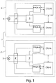
- FIG. 1 shows a control system 1 with two control circuits 2, 2', wherein each control circuit 2, 2' controls one signal lamp 3, 3' (here one-filament signal lamps).
- a lamp measure unit 4, 4' measures the actual rms current value of signal lamp 3, 3' and, optionally, the actual rms voltage value of signal lamp 3, 3'.
- the measured actual rms current value and, optionally, the actual rms voltage value are sent to two independent central processing units CPU-A, CPU-B.
- Both central processing units CPU-A, CPU-B comprise a memory where a desired rms current value for the respective signal lamp 3, 3' is stored.
- Each central processing unit CPU-A, CPU-B compares the measured actual rms current value with the desired rms current value and evaluates a correction current value.
- the central processing units CPU-A, CPU-B compare the correction current values. In case the correction values are consistent, each central processing unit CPU-A, CPU-B instruct a programmable logic device FPGS-A, FPGA-B to modulate the pulse width of a PWM control signal to reach the desired rms values accordingly. Therefore each programmable logic device FPGS-A, FPGA-B generates the PWM control signal which is sent to a power control device 5, 5'. The power control device 5, 5' switches the PWM signal to the signal lamp.
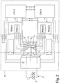
- FIG. 2 shows a control circuit 2" with a signal lamp 3" comprising two filaments 6, 7 for an inventive control system, wherein the second filament 7 is used as reserve in case of a failure of the first filament 6.
- a lamp measure unit 4" measures rms current and voltage values in both filaments 6, 7 of lamp 3" which are sent to the central processing units CPU-A, CPU-B.
- a power control device 5" comprises a transistor bridge with transistors T1, T2, T3, T4, T5, T6, wherein transistors T1, T2, T3 are controlled by the central processing unit CPU-A and the transistors T4, T5, T6 are controlled by the central processing unit CPU-B.
- the transistors T1, T2, T3, T4, T5, T6 are electrically connected such, that the PWM signal is only transferred in case both central processing units CPU-A, CPU-B evaluated the same correction current value for said specific signal lamp and both programmable logic devices FPGA-A, FPGA-B generate the same PWM signals for said specific signal lamp.
- the transistor bridge By means of the transistor bridge the polarity of the current can be switched, thereby generating AC current. In case of a one-filament-signal lamp the transistors T3, T6 can be omitted.
- Additional transistor T7, T8 are provided for carrying out a cold filament test in order to detect fault filaments even if they are not operated.
- the rms current value can be continuously adjusted for each cabling resistance by varying the duty cycle of a PWM signal.
- the invention realizes a safe control of signal incandescent lamps operated with low voltage in a short distance from the signal while the durability (life-time) of signal lamps can be increased, thereby decreasing maintenance costs. Since the desired rms values can be defined by the user, the same control system can be used for various types of signal lamps.
Landscapes
- Circuit Arrangement For Electric Light Sources In General (AREA)
- Traffic Control Systems (AREA)
Description
- The invention concerns a method and a control system for locally controlling at least two signal lamps for traffic applications.
- It is known to control signal lamps by means of an interlocking station. Yet, the control has to be carried out via long and for installation expensive cabling with a high voltage that has to be adjusted manually via bulky transformers near the lamps. Further the transformation of the voltage is involved with additional effort.
- Control installations located near the signal lamps allow using low DC voltage and a central voltage adjustment. The currents of the signal lamps are measured and the supply voltage is adjusted collectively for all signal lamps. As a result the emission of the different signal lamps may be different, depending on the specific environmental conditions, different parameters of different signal lamps or degradation of connections (corrosion of cables and clamps etc.). In particular when using low voltage these differences (in e.g. temperature, degree of degradation of connections) may result in great differences of lamp brightness which may lead to a declined visibility of the signals or, in case the correction current value is adapted such that the signal lamp having the lowest actual rms current value complies with the desired current value, durability of the other signal lamps is reduced due to the increased current which the lamps are exposed to.
- Prior art document
US 3,885,197 discloses a method and a system for controlling a plurality of signal lamps for traffic applications. A method for locally controlling a system comprising different lamps is known from prior art documentUS 6,031,749 , which discloses adjusting, for each of the different lamps, the lamp current based on a comparison of a measured rms lamp current and a desired rms current. - It is therefore an object of the invention to provide a method and a system for controlling signal lamps by low voltage signals, wherein degradation of single signal lamps do not lead to declined visibility of the signals and at the same time durability of the signal lamps is enhanced.
- This object is solved by the method according to
claim 1. - According to the invention steps a) through f) of this method are carried out for each signal lamp separately, wherein for each signal lamp individual correction values are evaluated. For each signal lamp a pulse width modulated signal (PWM-signal) is generated according to the desired rms current values independently of the adjustment of the current values of the other signal lamps, and the polarity of the PWM-signal is modulated.
- By adjusting the current to a specific rms current value for each signal lamp independently of the desired rms-values and the actual rms values of the other signal lamps, a uniform brightness for all signal lamps can be achieved. It is also possible to realize different predetermined brightness values for different signal lamps, if desired. Thus, a dedicated brightness can be achieved for each single signal lamp. No trade-off concerning the lamp brightness has to be made. The current can be adapted to different lamps reacting differently e.g. to environmental influences like cabling parameters. Thus, each lamp can be operated with an optimized rms current value. According to the invention AC current signals are generated by modulating the polarity of the PWM-signals, thereby preventing material migration within the lamp filament and thus further enhancing the durability of the lamp. The polarity is preferably changed every 10 ms so as to imitate 50 Hz AC. For generating the PWM signals it is preferred to use a programmable logic device, in particular a FPGA (field programmable gate array).
- It is highly preferred to carry out the method continuously in order to obtain safe information about the status of each signal lamp output at any time.
- The term "local control" means that the signal lamps are not controlled by the remote interlocking but by means of a control circuit which is located near the signal lamps, in particular at a distance in the range of up to about 100 m to the signal lamps. Due to a local control the signal lamps can be operated with low voltage (e.g. 12 V). No transformation of the voltage for current transport reason is required.
- The terms "rms current value" and "rms voltage value" describe the root mean square current and voltage values measured over a multitude of pulses.
- According to the invention the polarity of the PWM-signal is modulated by means of a transistor bridge comprising at least four transistors in order to modulate the polarity of the PWM-signal, wherein two of the transistors are controlled by a first central processing unit and the other transistors are controlled by a second central processing unit. The usage of a transistor bridge with at least four transistors, which are controlled by two different central processing units (CPUs) enables simulating an AC current signal which complies with a high safety level.
- The transistors of the transistor bridge are electrically connected such that the adjustment of step d) can only be applied to a specific signal lamp in case both central processing units evaluated the same correction current value for said specific signal lamp. Therefore, the current path of the PWM-signal always comprises one transistor controlled by the first CPU and one transistor controlled by the second CPU. Both transistors have to be switched to forward direction. Thus SIL4 safety for railway applications level can be realized.
- In order to provide signal lamps with equal brightness, the desired values can be chosen equal for all signal lamps.
- In a highly preferred variant the adjustment of the current is not carried out abruptly but within a predetermined adjustment time window, in particular within 5 - 300ms, preferably within 10 - 15 ms. I.e. in case of a current increase, in particular if a lamp is switched on, the current is gradually increased to avoid a high inrush current (soft start). Thereby the durability of the lamps is further enhanced.
- In particular it is advantageous if a short-circuit-monitoring is carried out during the adjustment time window. In case of a short circuit the short circuit can be detected during the current increase (current ramp) and the signal lamp can be switched off early before damage occurs due to an overcurrent.
- The invention also concerns the control system according to
claim 5 for carrying out a method as described before, the system comprising at least two control circuits, each control circuit controlling one signal lamp, wherein the control circuits comprise: two central processing units, two programmable logic devices having a PWM control for generating a PWM-signal, and a power control device, the power control device comprising a transistor bridge with at least four transistors in order to modulate the polarity of the PWM-signal, wherein two of the transistors are controlled by a first central processing unit and the other transistors are controlled by a second central processing unit. The control system is preferably connected to an interlocking e.g. via a CAN-network. - In order to minimize hardware costs it is preferred that at least two of the control circuits, preferably all control circuits of the control system, share the same central processing units and/or the same programmable logic devices.
- In case a two-filament signal lamp should be used it is advantageous if the transistor bridge comprises at least six transistors, wherein three of the transistors are controlled by the first central processing unit and the other transistors are controlled by the second central processing unit. Two of the transistors are then part of the current paths for both filaments.
- Further advantages can be extracted from the description and the enclosed drawings.
- The features mentioned above and below can be used in accordance with the invention either individually or collectively in any combination. The embodiments mentioned are not to be understood as exhaustive enumeration but rather have exemplary character for the description of the invention.
- The invention is shown in the drawing.
- FIG. 1
- shows a simplified control system with two control circuits.
- FIG. 2
- shows a control circuit with a two-filament signal lamp for an inventive control system.
-
FIG. 1 shows acontrol system 1 with twocontrol circuits 2, 2', wherein eachcontrol circuit 2, 2' controls onesignal lamp 3, 3' (here one-filament signal lamps). Alamp measure unit 4, 4' measures the actual rms current value ofsignal lamp 3, 3' and, optionally, the actual rms voltage value ofsignal lamp 3, 3'. The measured actual rms current value and, optionally, the actual rms voltage value are sent to two independent central processing units CPU-A, CPU-B. Both central processing units CPU-A, CPU-B comprise a memory where a desired rms current value for therespective signal lamp 3, 3' is stored. Each central processing unit CPU-A, CPU-B compares the measured actual rms current value with the desired rms current value and evaluates a correction current value. The central processing units CPU-A, CPU-B compare the correction current values. In case the correction values are consistent, each central processing unit CPU-A, CPU-B instruct a programmable logic device FPGS-A, FPGA-B to modulate the pulse width of a PWM control signal to reach the desired rms values accordingly. Therefore each programmable logic device FPGS-A, FPGA-B generates the PWM control signal which is sent to apower control device 5, 5'. Thepower control device 5, 5' switches the PWM signal to the signal lamp. - By measuring the voltage value besides the current value the central processing units CPU-A, CPU-B can compare if the current/voltage is inside a predefined window and so detect short circuits or lamps with broken filaments and also malfunctions in the transistor bridge or its control circuitry.
FIG. 2 shows acontrol circuit 2" with asignal lamp 3" comprising twofilaments second filament 7 is used as reserve in case of a failure of thefirst filament 6. Alamp measure unit 4" measures rms current and voltage values in bothfilaments lamp 3" which are sent to the central processing units CPU-A, CPU-B. In accordance with the description above, PWM signals are generated (here for bothfilaments 6, 7) by means of the programmable logic devices FPGA-A, FPGA-B. Apower control device 5" comprises a transistor bridge with transistors T1, T2, T3, T4, T5, T6, wherein transistors T1, T2, T3 are controlled by the central processing unit CPU-A and the transistors T4, T5, T6 are controlled by the central processing unit CPU-B. The transistors T1, T2, T3, T4, T5, T6 are electrically connected such, that the PWM signal is only transferred in case both central processing units CPU-A, CPU-B evaluated the same correction current value for said specific signal lamp and both programmable logic devices FPGA-A, FPGA-B generate the same PWM signals for said specific signal lamp. By means of the transistor bridge the polarity of the current can be switched, thereby generating AC current. In case of a one-filament-signal lamp the transistors T3, T6 can be omitted. - Additional transistor T7, T8 are provided for carrying out a cold filament test in order to detect fault filaments even if they are not operated.
- By measuring the current in both filaments of the lamp also short circuits between different lamps or their wiring can be detected. Therefore the current flow is enabled on one side only of the transistor bridge of another lamp and thus an electrical connection between both lamps can be detected.
- According to the invention the rms current value can be continuously adjusted for each cabling resistance by varying the duty cycle of a PWM signal. Thereby the invention realizes a safe control of signal incandescent lamps operated with low voltage in a short distance from the signal while the durability (life-time) of signal lamps can be increased, thereby decreasing maintenance costs. Since the desired rms values can be defined by the user, the same control system can be used for various types of signal lamps.
Claims (7)
- Method for controlling at least two signal lamps (3, 3', 3") for traffic applications,
characterized in
that each of the at least two signal lamps (3, 3', 3") is locally controlled by means of a control circuit (2, 2', 2") comprising at least a first central processing unit (CPU-A) and a second central processing unit (CPU-B), and in that the method comprises carrying out the following steps for each signal lamp (3, 3', 3"):a) defining a desired rms current value for a current through the respective signal lamp (3, 3', 3");b) measuring an actual rms current value of the current through the same signal lamp (3, 3', 3");c) sending the measured actual rms current value to each of the two independent central processing units (CPU-A, CPU-B);d) comparing, by means of each central processing unit (CPU-A, CPU-B), the respective actual rms current value with the desired rms current value and evaluating a correction current value;e) comparing, by means of the central processing units (CPU-A, CPU-B), the evaluated correction current values; andf) in case both central processing units (CPU-A, CPU-B) evaluated the same correction current value, adjusting the current to the desired rms current value by means of the control circuit (2, 2', 2"), wherein the control circuit (2, 2', 2") is powered by a constant voltage source,wherein the adjustment comprises generating for the same signal lamp (3, 3', 3") a pulse width modulated PWM-signal according to the desired rms current value independently of the adjustment of the current values of the other signal lamps (3, 3', 3") and wherein an AC current signal is generated by modulating the polarity of the PWM-signal by means of four transistors of a transistor bridge (T1, T2, T3, T4, T5, T6), wherein two of the transistors (T1, T2, T3) are controlled by the first central processing unit (CPU-A) and the other two transistors (T4, T5, T6) are controlled by the second central processing unit (CPU-B). - Method according to any one of the preceding claims, characterized in that the desired values are equal for all signal lamps (3, 3', 3").
- Method according to any one of the preceding claims, characterized in that in case of adjusting the current to higher values, the adjustment of the current is carried out gradually within a predetermined adjustment time window, in particular within 5 - 300ms, preferably within 10 - 15 ms.
- Method according to claim 3, characterized in that a short-circuit monitoring is carried out during the adjustment time window.
- Control system for controlling at least two signal lamps (3, 3', 3") for traffic applications, characterized in that the control system is adapted to carry out a method according to any one of the claim 1 through 4,
the system comprising at least two of the said control circuits (2, 2', 2"), each control circuit (2, 2', 2") controlling a separate signal lamp (3, 3', 3"), wherein each control circuit (2, 2', 2") comprises:a lamp measure unit (4, 4', 4") for measuring the actual rms current value of the current through the signal lamp (3, 3', 3") of the respective control circuit (2, 2', 2"),two programmable logic devices (FPGA-A, FPGA-B), each having a PWMcontrol (PWM-A, PWM-B) for generating the PWM-signal, the said first central processing unit (CPU-A) and the second central processing unit (CPU-B), anda power control device (5, 5', 5"), the power control device (5, 5, 5") comprising the said transistor bridge. - Control system according to claim 5 characterized in that at least two of the control circuits (2, 2', 2") share the same central processing units (CPU-A, CPU-B) and/or the same programmable logic devices (FPGA-A, FPGA-B).
- Control system according to claim 5 or 6 characterized in that the lamp is a two filament lamp and the transistor bridge comprises at least six transistors (T1, T2, T3, T4, T5, T6), wherein three of the transistors (T1, T2, T3) are controlled by the first central processing unit (CPU-A) and the other three transistors (T4, T5, T6) are controlled by the second central processing unit (CPU-B), wherein two of the transistors are part of current paths for both filaments.
Priority Applications (8)
| Application Number | Priority Date | Filing Date | Title |
|---|---|---|---|
| LTEP14194483.5T LT3024305T (en) | 2014-11-24 | 2014-11-24 | Method for locally controlling signal lamps for traffic applications and control system |
| EP14194483.5A EP3024305B1 (en) | 2014-11-24 | 2014-11-24 | Method for locally controlling signal lamps for traffic applications and control system |
| DK14194483.5T DK3024305T3 (en) | 2014-11-24 | 2014-11-24 | Method for local control of signal lights for traffic applications and control system |
| HUE14194483A HUE044127T2 (en) | 2014-11-24 | 2014-11-24 | Method for locally controlling signal lamps for traffic applications and control system |
| ES14194483T ES2719690T3 (en) | 2014-11-24 | 2014-11-24 | Method to locally control signal lamps for traffic applications and control system |
| PT14194483T PT3024305T (en) | 2014-11-24 | 2014-11-24 | Method for locally controlling signal lamps for traffic applications and control system |
| RS20190640A RS58760B1 (en) | 2014-11-24 | 2014-11-24 | Method for locally controlling signal lamps for traffic applications and control system |
| HRP20191047TT HRP20191047T1 (en) | 2014-11-24 | 2019-06-11 | Method for locally controlling signal lamps for traffic applications and control system |
Applications Claiming Priority (1)
| Application Number | Priority Date | Filing Date | Title |
|---|---|---|---|
| EP14194483.5A EP3024305B1 (en) | 2014-11-24 | 2014-11-24 | Method for locally controlling signal lamps for traffic applications and control system |
Publications (2)
| Publication Number | Publication Date |
|---|---|
| EP3024305A1 EP3024305A1 (en) | 2016-05-25 |
| EP3024305B1 true EP3024305B1 (en) | 2019-03-13 |
Family
ID=51951702
Family Applications (1)
| Application Number | Title | Priority Date | Filing Date |
|---|---|---|---|
| EP14194483.5A Active EP3024305B1 (en) | 2014-11-24 | 2014-11-24 | Method for locally controlling signal lamps for traffic applications and control system |
Country Status (8)
| Country | Link |
|---|---|
| EP (1) | EP3024305B1 (en) |
| DK (1) | DK3024305T3 (en) |
| ES (1) | ES2719690T3 (en) |
| HR (1) | HRP20191047T1 (en) |
| HU (1) | HUE044127T2 (en) |
| LT (1) | LT3024305T (en) |
| PT (1) | PT3024305T (en) |
| RS (1) | RS58760B1 (en) |
Family Cites Families (4)
| Publication number | Priority date | Publication date | Assignee | Title |
|---|---|---|---|---|
| US3885197A (en) * | 1974-02-01 | 1975-05-20 | Lear Siegler Inc | Light dimmer |
| US6031749A (en) * | 1999-03-31 | 2000-02-29 | Vari-Lite, Inc. | Universal power module |
| US7187139B2 (en) * | 2003-09-09 | 2007-03-06 | Microsemi Corporation | Split phase inverters for CCFL backlight system |
| CN101689059B (en) * | 2007-03-05 | 2015-04-29 | 塔西软件开发有限及两合公司 | Method and firmware for controlling voltage and current in a fluorescent lamp array |
-
2014
- 2014-11-24 LT LTEP14194483.5T patent/LT3024305T/en unknown
- 2014-11-24 PT PT14194483T patent/PT3024305T/en unknown
- 2014-11-24 RS RS20190640A patent/RS58760B1/en unknown
- 2014-11-24 EP EP14194483.5A patent/EP3024305B1/en active Active
- 2014-11-24 DK DK14194483.5T patent/DK3024305T3/en active
- 2014-11-24 HU HUE14194483A patent/HUE044127T2/en unknown
- 2014-11-24 ES ES14194483T patent/ES2719690T3/en active Active
-
2019
- 2019-06-11 HR HRP20191047TT patent/HRP20191047T1/en unknown
Non-Patent Citations (1)
| Title |
|---|
| None * |
Also Published As
| Publication number | Publication date |
|---|---|
| DK3024305T3 (en) | 2019-05-20 |
| HUE044127T2 (en) | 2019-09-30 |
| EP3024305A1 (en) | 2016-05-25 |
| RS58760B1 (en) | 2019-06-28 |
| LT3024305T (en) | 2019-06-10 |
| PT3024305T (en) | 2019-06-18 |
| ES2719690T3 (en) | 2019-07-12 |
| HRP20191047T1 (en) | 2019-09-06 |
Similar Documents
| Publication | Publication Date | Title |
|---|---|---|
| US20150280782A1 (en) | Method and device for transmitting data via a load line and lighting system | |
| US9603210B1 (en) | High speed, high current pulsed driver circuit | |
| US8432102B2 (en) | Systems and methods for multi-state switch networks | |
| RU2497316C2 (en) | Led excitation device | |
| US7336463B2 (en) | Device and method for dimming service loads | |
| US9554440B2 (en) | Dimmable LED lighting apparatus | |
| WO2013049524A1 (en) | Low cost led driver with integral dimming capability | |
| KR20110076798A (en) | Voltage Limiting Reverse Polarity Series LED Devices | |
| JP2008251227A (en) | Light-emitting device | |
| KR102261255B1 (en) | Apparatus for supplying at least one consumer with electrical energy or for providing electrical power for at least one consumer | |
| US10172196B2 (en) | Light unit driver system | |
| US9497813B2 (en) | LED lighting arrangement and method of controlling a LED lighting arrangement | |
| JP2014191933A (en) | Marker lamp device | |
| EP2952061B1 (en) | Device for led operation | |
| EP3024305A1 (en) | Method for locally controlling signal lamps for traffic applications and control system | |
| RU2570823C2 (en) | Data transmission system intended for datagrams transmission through load line | |
| US11632842B2 (en) | Selective inrush current control with active current clamp and monitoring | |
| EP2775798B1 (en) | Dimmable LED reading light unit, arrangement of power supply and dimmable LED reading light unit, method of operating a dimmable LED reading light unit in a power supply system, and method of replacing a dimmable light unit by a dimmable LED reading light unit | |
| US20140145645A1 (en) | Step-dimming led driver and system | |
| JP5674983B1 (en) | Remote control device for LED lighting power supply | |
| CN113366919B (en) | Dimmer switch and method for determining a low-end trim set point of a dimming control signal | |
| JP6106900B2 (en) | Constant power factor power supply and control method of constant power factor output | |
| US20150223302A1 (en) | Lighting color control method and system | |
| JP2020107433A (en) | Illumination control system and illumination system | |
| KR20170089337A (en) | Breakdown detecting apparatus of a railroad signal apparatus |
Legal Events
| Date | Code | Title | Description |
|---|---|---|---|
| AK | Designated contracting states |
Kind code of ref document: A1 Designated state(s): AL AT BE BG CH CY CZ DE DK EE ES FI FR GB GR HR HU IE IS IT LI LT LU LV MC MK MT NL NO PL PT RO RS SE SI SK SM TR |
|
| AX | Request for extension of the european patent |
Extension state: BA ME |
|
| PUAI | Public reference made under article 153(3) epc to a published international application that has entered the european phase |
Free format text: ORIGINAL CODE: 0009012 |
|
| 17P | Request for examination filed |
Effective date: 20160520 |
|
| RBV | Designated contracting states (corrected) |
Designated state(s): AL AT BE BG CH CY CZ DE DK EE ES FI FR GB GR HR HU IE IS IT LI LT LU LV MC MK MT NL NO PL PT RO RS SE SI SK SM TR |
|
| STAA | Information on the status of an ep patent application or granted ep patent |
Free format text: STATUS: EXAMINATION IS IN PROGRESS |
|
| 17Q | First examination report despatched |
Effective date: 20170103 |
|
| RAP1 | Party data changed (applicant data changed or rights of an application transferred) |
Owner name: THALES MANAGEMENT & SERVICES DEUTSCHLAND GMBH |
|
| REG | Reference to a national code |
Ref country code: DE Ref legal event code: R079 Ref document number: 602014042730 Country of ref document: DE Free format text: PREVIOUS MAIN CLASS: H05B0039040000 Ipc: H05B0037020000 |
|
| RIC1 | Information provided on ipc code assigned before grant |
Ipc: H05B 37/02 20060101AFI20180426BHEP Ipc: B61L 5/18 20060101ALI20180426BHEP Ipc: H05B 39/04 20060101ALI20180426BHEP |
|
| GRAP | Despatch of communication of intention to grant a patent |
Free format text: ORIGINAL CODE: EPIDOSNIGR1 |
|
| STAA | Information on the status of an ep patent application or granted ep patent |
Free format text: STATUS: GRANT OF PATENT IS INTENDED |
|
| INTG | Intention to grant announced |
Effective date: 20180601 |
|
| RIN1 | Information on inventor provided before grant (corrected) |
Inventor name: LOSTUN, VIRGIL Inventor name: HOLDER, HARTMUT Inventor name: WINGERATH, NORBERT Inventor name: WEISS, PETER Inventor name: D'ALIMONTE, SHAWN |
|
| GRAJ | Information related to disapproval of communication of intention to grant by the applicant or resumption of examination proceedings by the epo deleted |
Free format text: ORIGINAL CODE: EPIDOSDIGR1 |
|
| STAA | Information on the status of an ep patent application or granted ep patent |
Free format text: STATUS: EXAMINATION IS IN PROGRESS |
|
| RIN1 | Information on inventor provided before grant (corrected) |
Inventor name: WINGERATH, NORBERT Inventor name: WEISS, PETER Inventor name: D'ALIMONTE, SHAWN Inventor name: LOSTUN, VIRGIL Inventor name: HOLDER, HARTMUT |
|
| INTC | Intention to grant announced (deleted) | ||
| GRAP | Despatch of communication of intention to grant a patent |
Free format text: ORIGINAL CODE: EPIDOSNIGR1 |
|
| STAA | Information on the status of an ep patent application or granted ep patent |
Free format text: STATUS: GRANT OF PATENT IS INTENDED |
|
| INTG | Intention to grant announced |
Effective date: 20181004 |
|
| GRAS | Grant fee paid |
Free format text: ORIGINAL CODE: EPIDOSNIGR3 |
|
| GRAA | (expected) grant |
Free format text: ORIGINAL CODE: 0009210 |
|
| STAA | Information on the status of an ep patent application or granted ep patent |
Free format text: STATUS: THE PATENT HAS BEEN GRANTED |
|
| AK | Designated contracting states |
Kind code of ref document: B1 Designated state(s): AL AT BE BG CH CY CZ DE DK EE ES FI FR GB GR HR HU IE IS IT LI LT LU LV MC MK MT NL NO PL PT RO RS SE SI SK SM TR |
|
| REG | Reference to a national code |
Ref country code: GB Ref legal event code: FG4D |
|
| REG | Reference to a national code |
Ref country code: CH Ref legal event code: EP Ref country code: AT Ref legal event code: REF Ref document number: 1109488 Country of ref document: AT Kind code of ref document: T Effective date: 20190315 |
|
| REG | Reference to a national code |
Ref country code: IE Ref legal event code: FG4D |
|
| REG | Reference to a national code |
Ref country code: DE Ref legal event code: R096 Ref document number: 602014042730 Country of ref document: DE |
|
| REG | Reference to a national code |
Ref country code: CH Ref legal event code: NV Representative=s name: RIEDERER HASLER AND PARTNER PATENTANWAELTE AG, CH |
|
| REG | Reference to a national code |
Ref country code: RO Ref legal event code: EPE |
|
| REG | Reference to a national code |
Ref country code: DK Ref legal event code: T3 Effective date: 20190513 |
|
| REG | Reference to a national code |
Ref country code: NL Ref legal event code: FP |
|
| REG | Reference to a national code |
Ref country code: HR Ref legal event code: TUEP Ref document number: P20191047 Country of ref document: HR |
|
| REG | Reference to a national code |
Ref country code: EE Ref legal event code: FG4A Ref document number: E017370 Country of ref document: EE Effective date: 20190425 |
|
| REG | Reference to a national code |
Ref country code: PT Ref legal event code: SC4A Ref document number: 3024305 Country of ref document: PT Date of ref document: 20190618 Kind code of ref document: T Free format text: AVAILABILITY OF NATIONAL TRANSLATION Effective date: 20190607 |
|
| REG | Reference to a national code |
Ref country code: NO Ref legal event code: T2 Effective date: 20190313 |
|
| REG | Reference to a national code |
Ref country code: ES Ref legal event code: FG2A Ref document number: 2719690 Country of ref document: ES Kind code of ref document: T3 Effective date: 20190712 |
|
| PG25 | Lapsed in a contracting state [announced via postgrant information from national office to epo] |
Ref country code: SE Free format text: LAPSE BECAUSE OF FAILURE TO SUBMIT A TRANSLATION OF THE DESCRIPTION OR TO PAY THE FEE WITHIN THE PRESCRIBED TIME-LIMIT Effective date: 20190313 |
|
| REG | Reference to a national code |
Ref country code: GR Ref legal event code: EP Ref document number: 20190401523 Country of ref document: GR Effective date: 20190708 |
|
| REG | Reference to a national code |
Ref country code: HR Ref legal event code: T1PR Ref document number: P20191047 Country of ref document: HR |
|
| REG | Reference to a national code |
Ref country code: HU Ref legal event code: AG4A Ref document number: E044127 Country of ref document: HU |
|
| PG25 | Lapsed in a contracting state [announced via postgrant information from national office to epo] |
Ref country code: AL Free format text: LAPSE BECAUSE OF FAILURE TO SUBMIT A TRANSLATION OF THE DESCRIPTION OR TO PAY THE FEE WITHIN THE PRESCRIBED TIME-LIMIT Effective date: 20190313 Ref country code: SK Free format text: LAPSE BECAUSE OF FAILURE TO SUBMIT A TRANSLATION OF THE DESCRIPTION OR TO PAY THE FEE WITHIN THE PRESCRIBED TIME-LIMIT Effective date: 20190313 Ref country code: CZ Free format text: LAPSE BECAUSE OF FAILURE TO SUBMIT A TRANSLATION OF THE DESCRIPTION OR TO PAY THE FEE WITHIN THE PRESCRIBED TIME-LIMIT Effective date: 20190313 |
|
| PG25 | Lapsed in a contracting state [announced via postgrant information from national office to epo] |
Ref country code: SM Free format text: LAPSE BECAUSE OF FAILURE TO SUBMIT A TRANSLATION OF THE DESCRIPTION OR TO PAY THE FEE WITHIN THE PRESCRIBED TIME-LIMIT Effective date: 20190313 Ref country code: PL Free format text: LAPSE BECAUSE OF FAILURE TO SUBMIT A TRANSLATION OF THE DESCRIPTION OR TO PAY THE FEE WITHIN THE PRESCRIBED TIME-LIMIT Effective date: 20190313 |
|
| REG | Reference to a national code |
Ref country code: HR Ref legal event code: ODRP Ref document number: P20191047 Country of ref document: HR Payment date: 20191114 Year of fee payment: 6 |
|
| REG | Reference to a national code |
Ref country code: DE Ref legal event code: R097 Ref document number: 602014042730 Country of ref document: DE |
|
| PG25 | Lapsed in a contracting state [announced via postgrant information from national office to epo] |
Ref country code: IS Free format text: LAPSE BECAUSE OF FAILURE TO SUBMIT A TRANSLATION OF THE DESCRIPTION OR TO PAY THE FEE WITHIN THE PRESCRIBED TIME-LIMIT Effective date: 20190713 |
|
| PLBE | No opposition filed within time limit |
Free format text: ORIGINAL CODE: 0009261 |
|
| STAA | Information on the status of an ep patent application or granted ep patent |
Free format text: STATUS: NO OPPOSITION FILED WITHIN TIME LIMIT |
|
| 26N | No opposition filed |
Effective date: 20191216 |
|
| PG25 | Lapsed in a contracting state [announced via postgrant information from national office to epo] |
Ref country code: SI Free format text: LAPSE BECAUSE OF FAILURE TO SUBMIT A TRANSLATION OF THE DESCRIPTION OR TO PAY THE FEE WITHIN THE PRESCRIBED TIME-LIMIT Effective date: 20190313 |
|
| PG25 | Lapsed in a contracting state [announced via postgrant information from national office to epo] |
Ref country code: MC Free format text: LAPSE BECAUSE OF FAILURE TO SUBMIT A TRANSLATION OF THE DESCRIPTION OR TO PAY THE FEE WITHIN THE PRESCRIBED TIME-LIMIT Effective date: 20190313 |
|
| REG | Reference to a national code |
Ref country code: BE Ref legal event code: MM Effective date: 20191130 |
|
| PG25 | Lapsed in a contracting state [announced via postgrant information from national office to epo] |
Ref country code: IE Free format text: LAPSE BECAUSE OF NON-PAYMENT OF DUE FEES Effective date: 20191124 |
|
| PG25 | Lapsed in a contracting state [announced via postgrant information from national office to epo] |
Ref country code: BE Free format text: LAPSE BECAUSE OF NON-PAYMENT OF DUE FEES Effective date: 20191130 |
|
| REG | Reference to a national code |
Ref country code: HR Ref legal event code: ODRP Ref document number: P20191047 Country of ref document: HR Payment date: 20201116 Year of fee payment: 7 |
|
| PG25 | Lapsed in a contracting state [announced via postgrant information from national office to epo] |
Ref country code: CY Free format text: LAPSE BECAUSE OF FAILURE TO SUBMIT A TRANSLATION OF THE DESCRIPTION OR TO PAY THE FEE WITHIN THE PRESCRIBED TIME-LIMIT Effective date: 20190313 |
|
| REG | Reference to a national code |
Ref country code: AT Ref legal event code: UEP Ref document number: 1109488 Country of ref document: AT Kind code of ref document: T Effective date: 20190313 |
|
| PG25 | Lapsed in a contracting state [announced via postgrant information from national office to epo] |
Ref country code: MT Free format text: LAPSE BECAUSE OF FAILURE TO SUBMIT A TRANSLATION OF THE DESCRIPTION OR TO PAY THE FEE WITHIN THE PRESCRIBED TIME-LIMIT Effective date: 20190313 |
|
| REG | Reference to a national code |
Ref country code: HR Ref legal event code: ODRP Ref document number: P20191047 Country of ref document: HR Payment date: 20211122 Year of fee payment: 8 |
|
| PG25 | Lapsed in a contracting state [announced via postgrant information from national office to epo] |
Ref country code: MK Free format text: LAPSE BECAUSE OF FAILURE TO SUBMIT A TRANSLATION OF THE DESCRIPTION OR TO PAY THE FEE WITHIN THE PRESCRIBED TIME-LIMIT Effective date: 20190313 |
|
| REG | Reference to a national code |
Ref country code: HR Ref legal event code: ODRP Ref document number: P20191047 Country of ref document: HR Payment date: 20221122 Year of fee payment: 9 |
|
| REG | Reference to a national code |
Ref country code: HR Ref legal event code: ODRP Ref document number: P20191047 Country of ref document: HR Payment date: 20231026 Year of fee payment: 10 |
|
| P01 | Opt-out of the competence of the unified patent court (upc) registered |
Free format text: CASE NUMBER: APP_35448/2024 Effective date: 20240613 |
|
| REG | Reference to a national code |
Ref country code: HR Ref legal event code: ODRP Ref document number: P20191047 Country of ref document: HR Payment date: 20241024 Year of fee payment: 11 |
|
| REG | Reference to a national code |
Ref country code: CH Ref legal event code: U11 Free format text: ST27 STATUS EVENT CODE: U-0-0-U10-U11 (AS PROVIDED BY THE NATIONAL OFFICE) Effective date: 20251201 |
|
| REG | Reference to a national code |
Ref country code: HR Ref legal event code: ODRP Ref document number: P20191047 Country of ref document: HR Payment date: 20251110 Year of fee payment: 12 |
|
| PGFP | Annual fee paid to national office [announced via postgrant information from national office to epo] |
Ref country code: PT Payment date: 20251118 Year of fee payment: 12 |
|
| PGFP | Annual fee paid to national office [announced via postgrant information from national office to epo] |
Ref country code: HU Payment date: 20251112 Year of fee payment: 12 |
|
| PGFP | Annual fee paid to national office [announced via postgrant information from national office to epo] |
Ref country code: LU Payment date: 20251113 Year of fee payment: 12 Ref country code: NL Payment date: 20251112 Year of fee payment: 12 |
|
| PGFP | Annual fee paid to national office [announced via postgrant information from national office to epo] |
Ref country code: DE Payment date: 20251028 Year of fee payment: 12 |
|
| PGFP | Annual fee paid to national office [announced via postgrant information from national office to epo] |
Ref country code: LT Payment date: 20251103 Year of fee payment: 12 Ref country code: GB Payment date: 20251023 Year of fee payment: 12 |
|
| PGFP | Annual fee paid to national office [announced via postgrant information from national office to epo] |
Ref country code: NO Payment date: 20251113 Year of fee payment: 12 |
|
| PGFP | Annual fee paid to national office [announced via postgrant information from national office to epo] |
Ref country code: AT Payment date: 20251027 Year of fee payment: 12 |
|
| PGFP | Annual fee paid to national office [announced via postgrant information from national office to epo] |
Ref country code: FI Payment date: 20251113 Year of fee payment: 12 Ref country code: DK Payment date: 20251112 Year of fee payment: 12 Ref country code: IT Payment date: 20251030 Year of fee payment: 12 |
|
| PGFP | Annual fee paid to national office [announced via postgrant information from national office to epo] |
Ref country code: HR Payment date: 20251110 Year of fee payment: 12 Ref country code: FR Payment date: 20251117 Year of fee payment: 12 |
|
| PGFP | Annual fee paid to national office [announced via postgrant information from national office to epo] |
Ref country code: GR Payment date: 20251029 Year of fee payment: 12 Ref country code: TR Payment date: 20251120 Year of fee payment: 12 |
|
| PGFP | Annual fee paid to national office [announced via postgrant information from national office to epo] |
Ref country code: CH Payment date: 20251201 Year of fee payment: 12 |
|
| PGFP | Annual fee paid to national office [announced via postgrant information from national office to epo] |
Ref country code: LV Payment date: 20251104 Year of fee payment: 12 |
|
| PGFP | Annual fee paid to national office [announced via postgrant information from national office to epo] |
Ref country code: BG Payment date: 20251031 Year of fee payment: 12 |
|
| PGFP | Annual fee paid to national office [announced via postgrant information from national office to epo] |
Ref country code: EE Payment date: 20251113 Year of fee payment: 12 |
|
| PGFP | Annual fee paid to national office [announced via postgrant information from national office to epo] |
Ref country code: RO Payment date: 20251105 Year of fee payment: 12 |
|
| PGFP | Annual fee paid to national office [announced via postgrant information from national office to epo] |
Ref country code: RS Payment date: 20251105 Year of fee payment: 12 |
|
| PGFP | Annual fee paid to national office [announced via postgrant information from national office to epo] |
Ref country code: ES Payment date: 20251211 Year of fee payment: 12 |