EP3023842A1 - Chassis structure, optical scanning device, and image forming apparatus - Google Patents
Chassis structure, optical scanning device, and image forming apparatus Download PDFInfo
- Publication number
- EP3023842A1 EP3023842A1 EP15190875.3A EP15190875A EP3023842A1 EP 3023842 A1 EP3023842 A1 EP 3023842A1 EP 15190875 A EP15190875 A EP 15190875A EP 3023842 A1 EP3023842 A1 EP 3023842A1
- Authority
- EP
- European Patent Office
- Prior art keywords
- chassis
- cover member
- image forming
- structure according
- chassis structure
- Prior art date
- Legal status (The legal status is an assumption and is not a legal conclusion. Google has not performed a legal analysis and makes no representation as to the accuracy of the status listed.)
- Granted
Links
Images



Classifications
-
- G—PHYSICS
- G03—PHOTOGRAPHY; CINEMATOGRAPHY; ANALOGOUS TECHNIQUES USING WAVES OTHER THAN OPTICAL WAVES; ELECTROGRAPHY; HOLOGRAPHY
- G03G—ELECTROGRAPHY; ELECTROPHOTOGRAPHY; MAGNETOGRAPHY
- G03G21/00—Arrangements not provided for by groups G03G13/00 - G03G19/00, e.g. cleaning, elimination of residual charge
- G03G21/16—Mechanical means for facilitating the maintenance of the apparatus, e.g. modular arrangements
- G03G21/1604—Arrangement or disposition of the entire apparatus
- G03G21/1619—Frame structures
-
- G—PHYSICS
- G03—PHOTOGRAPHY; CINEMATOGRAPHY; ANALOGOUS TECHNIQUES USING WAVES OTHER THAN OPTICAL WAVES; ELECTROGRAPHY; HOLOGRAPHY
- G03G—ELECTROGRAPHY; ELECTROPHOTOGRAPHY; MAGNETOGRAPHY
- G03G15/00—Apparatus for electrographic processes using a charge pattern
- G03G15/04—Apparatus for electrographic processes using a charge pattern for exposing, i.e. imagewise exposure by optically projecting the original image on a photoconductive recording material
- G03G15/04036—Details of illuminating systems, e.g. lamps, reflectors
- G03G15/04045—Details of illuminating systems, e.g. lamps, reflectors for exposing image information provided otherwise than by directly projecting the original image onto the photoconductive recording material, e.g. digital copiers
-
- G—PHYSICS
- G02—OPTICS
- G02B—OPTICAL ELEMENTS, SYSTEMS OR APPARATUS
- G02B26/00—Optical devices or arrangements for the control of light using movable or deformable optical elements
- G02B26/08—Optical devices or arrangements for the control of light using movable or deformable optical elements for controlling the direction of light
- G02B26/10—Scanning systems
- G02B26/12—Scanning systems using multifaceted mirrors
-
- G—PHYSICS
- G02—OPTICS
- G02B—OPTICAL ELEMENTS, SYSTEMS OR APPARATUS
- G02B26/00—Optical devices or arrangements for the control of light using movable or deformable optical elements
- G02B26/08—Optical devices or arrangements for the control of light using movable or deformable optical elements for controlling the direction of light
- G02B26/10—Scanning systems
- G02B26/12—Scanning systems using multifaceted mirrors
- G02B26/121—Mechanical drive devices for polygonal mirrors
- G02B26/122—Control of the scanning speed of the polygonal mirror
-
- G—PHYSICS
- G03—PHOTOGRAPHY; CINEMATOGRAPHY; ANALOGOUS TECHNIQUES USING WAVES OTHER THAN OPTICAL WAVES; ELECTROGRAPHY; HOLOGRAPHY
- G03G—ELECTROGRAPHY; ELECTROPHOTOGRAPHY; MAGNETOGRAPHY
- G03G15/00—Apparatus for electrographic processes using a charge pattern
- G03G15/04—Apparatus for electrographic processes using a charge pattern for exposing, i.e. imagewise exposure by optically projecting the original image on a photoconductive recording material
- G03G15/04036—Details of illuminating systems, e.g. lamps, reflectors
-
- G—PHYSICS
- G03—PHOTOGRAPHY; CINEMATOGRAPHY; ANALOGOUS TECHNIQUES USING WAVES OTHER THAN OPTICAL WAVES; ELECTROGRAPHY; HOLOGRAPHY
- G03G—ELECTROGRAPHY; ELECTROPHOTOGRAPHY; MAGNETOGRAPHY
- G03G21/00—Arrangements not provided for by groups G03G13/00 - G03G19/00, e.g. cleaning, elimination of residual charge
- G03G21/16—Mechanical means for facilitating the maintenance of the apparatus, e.g. modular arrangements
- G03G21/1661—Mechanical means for facilitating the maintenance of the apparatus, e.g. modular arrangements means for handling parts of the apparatus in the apparatus
- G03G21/1666—Mechanical means for facilitating the maintenance of the apparatus, e.g. modular arrangements means for handling parts of the apparatus in the apparatus for the exposure unit
-
- H—ELECTRICITY
- H04—ELECTRIC COMMUNICATION TECHNIQUE
- H04N—PICTORIAL COMMUNICATION, e.g. TELEVISION
- H04N1/00—Scanning, transmission or reproduction of documents or the like, e.g. facsimile transmission; Details thereof
- H04N1/00519—Constructional details not otherwise provided for, e.g. housings, covers
-
- H—ELECTRICITY
- H04—ELECTRIC COMMUNICATION TECHNIQUE
- H04N—PICTORIAL COMMUNICATION, e.g. TELEVISION
- H04N1/00—Scanning, transmission or reproduction of documents or the like, e.g. facsimile transmission; Details thereof
- H04N1/00519—Constructional details not otherwise provided for, e.g. housings, covers
- H04N1/00559—Mounting or support of components or elements
-
- H—ELECTRICITY
- H04—ELECTRIC COMMUNICATION TECHNIQUE
- H04N—PICTORIAL COMMUNICATION, e.g. TELEVISION
- H04N1/00—Scanning, transmission or reproduction of documents or the like, e.g. facsimile transmission; Details thereof
- H04N1/04—Scanning arrangements, i.e. arrangements for the displacement of active reading or reproducing elements relative to the original or reproducing medium, or vice versa
- H04N1/06—Scanning arrangements, i.e. arrangements for the displacement of active reading or reproducing elements relative to the original or reproducing medium, or vice versa using cylindrical picture-bearing surfaces, i.e. scanning a main-scanning line substantially perpendicular to the axis and lying in a curved cylindrical surface
- H04N1/0607—Scanning a concave surface, e.g. with internal drum type scanners
Definitions
- the present invention relates to a chassis structure, an optical scanning device, and an image forming apparatus.
- optical image information is formed on a previously uniformly charged image bearer, such as a photoconductor, by an optical scanning device so that an electrostatic latent image is obtained, the electrostatic latent image is visualized by using toner from a developing device, a visible image is transferred onto a recording medium, such as a transfer sheet, directly or via an intermediate transfer member, such as an intermediate transfer belt, an unfixed toner image on the recording medium is fixed by a fixing device that uses pressure, heat, and/or the like, whereby an image is formed.
- a previously uniformly charged image bearer such as a photoconductor
- the optical scanning device uses an LD array (hereinafter, referred to as the LDA), a vertical-cavity surface-emitting laser (hereinafter, referred to as the VCSEL), or the like, and thus the quality/the image quality has been enhanced by increasing channels of luminous points.
- LDA LD array
- VCSEL vertical-cavity surface-emitting laser
- the optical scanning device of the image forming apparatus that is described in Japanese Laid-open Patent Publication No. 2014-12368 has a problem in that, as the seal member is complicated or is divided into multiple pieces by necessity, the yield rate of sheet materials is low and the costs are increased. Furthermore, as seal members have a joint line, a clearance occurs at the joint line, which results in a problem of a reduction in the sealing capability. Furthermore, there is a possibility that a sponge member is fragmented due to hydrolysis that is caused by water (moistures), or the like, with the passage of time, and the fragmented sponge member enters the image forming apparatus as a foreign matter. As a result, there is a problem of the occurrence of faulty images, such as image voids.
- a chassis structure includes: a chassis that houses a component used for an image forming apparatus inside and that includes an opening; a cover member that covers the opening of the chassis; and a seal member that is provided between the cover member and the chassis and that, when the cover member is attached to the chassis, is compressed and deformed so as to seal a gap between the cover member and the chassis.
- An attached section of the cover member to which the seal member is attached is provided with a hole.
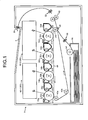
- FIG. 1 illustrates a schematic cross-sectional view of a full-color printer that is an example of the image forming apparatus.
- the image forming apparatus 1, which is illustrated in FIG. 1 includes an electrophotographic image forming part, and the image forming part includes four image forming units 10a, 10b, 10c, and 10d.
- the first to fourth image forming units 10a, 10b, 10c, and 10d have the same configuration; however, they are different only in the corresponding toner color, and each of the image forming units forms, for example, black toner images, magenta toner images, cyan toner images, or yellow toner images.
- the image forming units have the same configuration except that they have different developer (toner) colors; therefore, in the following explanation, they are explained without the accompanied characters a, b, c, and d as appropriate.
- An image forming unit 10 is provided with a photoconductor 30 that is a drum-shaped image bearer.
- a charging member 32, a developing device 33, and a cleaning device 31 are provided around the photoconductor 30.
- the photoconductor 30 can be driven to rotate in a clockwise direction and, when a predetermined bias voltage is applied to the charging member 32, the surface of the photoconductor 30, which is driven to rotate, can be uniformly charged.
- the non-contact type charging member 32 that uses corona discharge, or the like, is used; however, it is possible to use a roller-shaped member that is in contact with the photoconductor 30.
- the optical scanning device 60 is located above the four image forming units 10.
- the optical scanning device 60 includes an M-Y unit 60-1 that performs exposure and scanning on photoconductor drums 30a and 30b and a Bk-C unit 60-2 that performs exposure and scanning on photoconductor drums 30c and 30d.
- the optical scanning device 60 causes the surface of the corresponding photoconductor drum 30 to be irradiated with a scanning light due to lighting control based on image information, thereby forming electrostatic latent images. After an electrostatic latent image is formed on the photoconductor 30 by the optical scanning device 60, it is passed by the developing device 33 in accordance with the rotation of the photoconductor 30 so that it is developed with applied toner of each color, whereby it is visualized.
- An endless-belt type intermediate transfer belt 40 which is configured as an intermediate transfer member, is provided such that it is opposed to the photoconductor 30 of each of the image forming units 10. Each of the photoconductors 30 is in contact with the surface of the intermediate transfer belt 40.
- the intermediate transfer belt 40 is configured such that it is wrapped around multiple support rollers (40a, 40b, and 40c), and the support roller 40c is connected to a drive motor that is a driving source. When the drive motor is driven, the intermediate transfer belt 40 is moved and rotated in a counterclockwise direction in the drawing (see the direction of the arrow in FIG. 1 ), and the support rollers 40a and 40b, which can be driven to rotate, are driven to rotate in accordance with the rotation of the intermediate transfer belt 40.
- a primary transfer roller is provided on the back surface of the intermediate transfer belt 40 such that it is opposed to the photoconductor 30 with the belt interposed therebetween.
- a primary transfer bias is applied to the primary transfer roller from a high-voltage power source so that a toner image, which has been developed by the developing device 33, is primarily transferred onto the intermediate transfer belt 40.
- the primary-transfer residual toner that has not been primarily transferred and that remains on the photoconductor 30, it is removed by a cleaning blade that is provided in the cleaning device 31 so that it stands by for the next image forming operation by the photoconductor 30.
- a secondary transfer charger 48 is provided as a secondary transfer device at the position that is opposed to the support roller 40c with the intermediate transfer belt 40 interposed therebetween.
- the secondary transfer charger 48 is located away from the intermediate transfer belt 40 by a predetermined distance. The voltage with the polarity opposite to that of the charging member 32 is applied to the secondary transfer charger 48.
- the image forming apparatus 1 includes a pair of registration rollers (a pair of position setting rollers) 56, or the like, in addition to a sheet feeding cassette 59 on which a recording medium is stacked and a sheet feeding roller 54. Furthermore, a fixing device 50 is located downstream of the secondary transfer charger 48 with respect to the conveying direction of the recording medium, and it includes a pair of rollers, i.e., a pressing roller and a heating roller, and applies heat and pressure to a recording medium to fix an unfixed toner image to the recording medium.
- a pair of rollers i.e., a pressing roller and a heating roller
- a pair of conveyance rollers 52, a pair of paper ejection rollers 58, or the like that ejects a recording medium, which is delivered from the fixing device 50, to a recording-medium discharge unit, such as a paper ejection tray 5.
- the photoconductor 30 When an image formation signal is received from a personal computer, or the like, the photoconductor 30 is started to be driven and rotated in a clockwise direction by a driving source. At this point, the surface of the photoconductor 30 is irradiated with a light from a neutralization device so that the surface potential is initialized. After the surface potential is initialized, the surface of the photoconductor 30 is uniformly charged by the charging member 32 so as to have a predetermined polarity. The charged surface of the photoconductor 30 is irradiated with a laser light from the optical scanning device 60. Thus, a desired electrostatic latent image is formed on the surface of the photoconductor 30.
- the image information with which the optical scanning device 60 conducts exposure and optical scanning on each of the photoconductors 30 is the single-color image information that is obtained by separating a desired full-color image into each piece of toner color information of yellow, cyan, magenta, and black.
- each color toner developer
- each color toner is applied to the electrostatic latent image from the developing device 33, whereby it is visualized as a developed toner image.
- the intermediate transfer belt 40 is driven to move in a counterclockwise direction in the drawing.
- the primary transfer voltage that is applied to the primary transfer roller has the polarity opposite to the toner charging polarity of the toner image that is formed on the photoconductor 30. Due to the effect of the primary transfer voltage, a primary-transfer electric field is formed between the photoconductor 30 and the intermediate transfer belt 40.
- the toner image on the photoconductor 30 is electrostatically and primarily transferred onto the intermediate transfer belt 40 that is driven to rotate in synchronization with the photoconductor 30.
- the toner image of each color which is primarily transferred as described above, is sequentially superimposed on the intermediate transfer belt 40 in synchronized timing, starting from the upstream side of the intermediate transfer belt 40 with respect to the conveying direction, whereby a desired full-color toner image is formed on the intermediate transfer belt 40.
- a recording medium on which an image is to be formed is appropriately separated one by one from the bundle of recording media that is stacked on the sheet feeding cassette 59 due to the action of an appropriate conveying member, such as the sheet feeding roller 54, until the pair of registration rollers 56.
- an appropriate conveying member such as the sheet feeding roller 54
- the end of the conveyed recording medium is brought into contact with the nip section of the pair of registration rollers 56, and what is called a loop is formed, whereby a registration is conducted on the recording medium.
- the pair of registration rollers 56 starts to be driven to rotate in synchronized timing with the full-color toner image that is borne on the intermediate transfer belt 40.
- the recording medium is delivered toward the secondary transfer unit that includes the secondary transfer charger 48 that is opposed to the support roller 40c with the intermediate transfer belt 40 interposed therebetween by a predetermined space.
- a predetermined transfer voltage is applied to the secondary transfer charger 48 so that the full-color toner image that is formed on the surface of the intermediate transfer belt 40 is collectively transferred onto the recording medium.
- the recording medium is conveyed to the fixing device 50 and, when it is passed by the fixing device 50, heat and pressure are applied to it by the fixing device 50, whereby a semipermanent full-color image is fixed to the recording medium.
- the recording medium is discharged to the recording-medium discharge unit, such as the paper ejection tray 5, via the pair of conveyance rollers 52, the pair of paper ejection rollers 58, or the like.
- the residual toner which is not transferred by the secondary transfer unit that is provided with the secondary transfer charger 48 and which remains on the intermediate transfer belt 40, is removed and collected by an intermediate-transfer belt cleaning unit.
- the optical scanning device 60 includes the M-Y unit 60-1 that conducts exposure scanning on the photoconductor drums 30a and 30b and the Bk-C unit 60-2 that conducts exposure scanning on the photoconductor drums 30c and 30d.
- the M-Y unit 60-1 and the Bk-C unit 60-2 have the same optical axis layout, the Bk-C unit 60-2 is explained, and the explanation of the M-Y unit 60-1 is omitted.
- FIG. 2 is a configuration diagram that schematically illustrates an optical incidence system of the Bk-C unit 60-2.
- a light source unit 61 that emits a laser light includes a light source 61-1 that emits a laser light by using a linearly-polarized light; a 1/4 wave plate 61-4 that converts a laser light into a circularly-polarized light; a collimator lens 61-5 that converts the laser light on which polarization conversion has been performed by the 1/4 wave plate into a parallel light; and an aperture 61-6 that obtains the parallel laser light.
- the light source 61-1 is, for example, a laser diode (LD), a laser diode array (LDA), or a vertical-cavity surface-emitting laser (VCSEL), and it includes multiple emission points. These optical elements are assembled and held within a light-source holder in an integrated manner. After a laser light is emitted from the light source unit 61, it passes through the optical incidence system and enters a deflector 72 that is an optical deflecting unit.
- LD laser diode
- LDA laser diode array
- VCSEL vertical-cavity surface-emitting laser
- the optical incidence system which forms a beam profile, includes a prism beam splitter (PBS) 73 that splits the laser light, which is emitted from the light source unit 61, in two directions on the sub-scanning cross-sectional surface; a 1/4 wave plate 74 that converts a linearly-polarized light into a circularly-polarized light with regard to polarization of the laser that has been split in two directions; and a cylindrical lens (CYL) 75 that obtains the power only on the sub-scanning cross-sectional surface with respect to a laser light, which has been converted into a circularly-polarized light, and that focuses it on the mirror surface of a rotary polygon mirror 72b that is provided in the deflector 72.
- PBS prism beam splitter
- CYL cylindrical lens
- a laser light After a laser light is formed by the optical incidence system, it is focused on the mirror surface of each of the rotary polygon mirrors 72b of the deflector 72.
- the deflector 72 drives the rotary polygon mirror 72b at a desired rotating speed in a stable manner. As described above, as a laser light enters the mirror surface of the rotary polygon mirror 72b, scanning is conducted with the laser light in a main-scanning direction.
- FIG. 3 is a configuration diagram that schematically illustrates the optical scanning system.
- a laser light with which the rotary polygon mirror 72b in the upper tier is scanned, passes through a first output lens (L1) 81, a second output lens (L2) 82, and a dust prevention glass 85 so that the surface of the photoconductor drum 30 is scanned at a constant speed, whereby an electrostatic latent image is formed.
- mirrors 83a, 83b, and 83c that reflect a laser light.
- a laser light with which the rotary polygon mirror 72b in the lower tier is scanned, passes through the first output lens 81, the second output lens 82, and the dust prevention glass 85 so that the surface of the photoconductor drum 30 is scanned at a constant speed, whereby an electrostatic latent image is formed.
- a mirror 84 On the optical path is provided a mirror 84 that reflects a laser light.
- the optical scanning system, the optical incidence system, and the deflector are integrally attached to an optical housing 90, whereby the characteristics of the optical scanning device 60 are ensured.
- the deflector 72 is provided with the rotary polygon mirror 72b, and it is attached to a motor board 72a.
- the rotary polygon mirror 72b includes four mirror surfaces, and it has a two-tier structure.
- An upper tier 72-2 and a lower tier 72-1 of the rotary polygon mirror 72b are formed such that they are shifted by ⁇ in a rotation direction.
- the upper tier 72-2 of the rotary polygon mirror 72b conducts scanning on the photoconductor drum 30d
- the lower tier 72-1 of the rotary polygon mirror 72b conducts scanning on the photoconductor drum 30c. They do not conduct scanning simultaneously due to their geometries, and they are configured to conduct exposure scanning on the basis of the image information that corresponds to each station.
- FIG. 5 is an explanatory diagram that illustrates the prism beam splitter 73 that splits a laser light into two. After a laser light (a light flux A) is emitted from the light source unit 61, it is converted from a linearly-polarized light into a circularly-polarized light by the 1/4 wave plate 61-4 of the light source unit 61.
- a laser light a light flux A
- the laser light (the light flux A), which has the characteristics of circularly-polarized light, reaches a polarization separation surface 73a of the prism beam splitter 73, only the S polarized light that is the component perpendicular to the mirror surface (reflection surface) of the rotary polygon mirror 72b is transmitted through the polarization separation surface 73a among the polarization components of the circularly-polarized light.
- the laser light (the light flux A), which has the characteristics of circularly-polarized light
- the P polarized light that is the component parallel to the mirror surface (reflection surface) of the rotary polygon mirror 72b is reflected by the polarization separation surface 73a among the polarization components of the circularly-polarized light.
- the laser light is reflected by the polarization separation surface 73a, it is reflected by a reflection mirror surface 73b of the prism beam splitter 73.
- the single laser light is split into two laser lights that have different polarization characteristics (hereinafter, referred to as the light flux split). After each laser light is subjected to the light flux split, it is transmitted through the prism beam splitter 73 and is then converted into a circularly-polarized light again by the 1/4 wave plate 74.
- FIG. 6 is an explanatory diagram that illustrates the sealing structure of the optical scanning device 60.
- a first cover member 91 and a second cover member 92 are attached to openings of the optical housing 90 that houses each optical element inside.
- a viscoelastic member B which is a seal member made of a resin, synthetic rubber, or the like, is interposed in the gap that is present between the cover members 91, 92 and the optical housing 90, whereby the sealing performance is ensured.
- the number of cover members is not limited to this configuration, and it may be at least one.
- the first cover member 91 and the second cover member 92 are the members to which the viscoelastic member B is attached.
- the cover members 91 and 92 have a box shape with an opening that is formed on one surface, and they include outer wall sections 91g and 92g that rise from the outer circumference of the bottom section. Furthermore, they include inner wall sections 91h and 92h that are provided inside the outer wall sections 91g and 92g.
- the viscoelastic member B is heated, it is poured by a melter, or the like, and is cooled so as to be hardened in the area that is surrounded by the outer wall sections 91g, 92g of the cover members 91, 92, the inner wall sections 91h, 92h, and attached surfaces 91e, 92e that are on the bottom section and that are sandwiched between the outer wall sections 91g, 92g and the inner wall sections 91h, 92h.
- the viscoelastic member B is attached to the first cover member 91 and the second cover member 92.
- the attached sections of the viscoelastic member B are the outer wall sections 91g, 92g, the inner wall sections 91h, 92h, and the attached surfaces 91e, 92e.
- the deflector and the light source are often replaced due to the operating life, degradation, or the like.
- the deflector or the light source it is necessary to remove the first cover member 91 or the second cover member 92 according to the present embodiment. If the first cover member 91 and the second cover member 92 are removed, the viscoelastic member B adheres to the optical housing 90 and is sometimes separated from the cover members 91 and 92 that are the attached members.
- an adhesive such as a double-sided tape
- a seal member which is an elastic body such as sponge.
- an elastic body, such as sponge is in contact with an attachment target member, such as an optical housing; therefore, when the deflector or the light source is replaced, the seal member is not separated from the attached member.
- the seal member that includes sponge, or the like, used to ensure the sealing performance is typically made of foamed polyurethane (foamed PU), or the like, and therefore hydrolysis occurs due to water (moisture), or the like, with the passage of time. If hydrolysis occurs in the foamed PU, the joints of the seal member that includes sponge, or the like, are separated, and the fragments thereof are dropped in the surroundings. Then, there is a possibility that the seal member in fragments enters the image forming apparatus as a foreign matter. As a result, there is the problem of the occurrence of faulty images, such as image voids.
- seal members with a double-sided tape are typically formed by performing punching processing on a large sheet, the shape of the seal member is often complicated. Therefore, the number of seal members that can be obtained from a single sheet of a basic size is small, and the yield rate is low.
- seal members with a double-sided tape are often configured to be split, the gap that occurs in the joint line between seal members during assembling cannot be completely removed, and the sealing performance is insufficient.
- the invention according to the present embodiment also solves this problem.
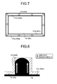
- multiple holes 91f and 92f are provided on the attached surfaces 91e and 92e of the cover members 91 and 92.
- the holes 91f, 92f are provided between the outer wall sections 91g, 92g and the inner wall sections 91h, 92h on the bottom section.
- the holes 91f and 92f have a cylindrical shape that protrudes toward the opposite side of the attached surfaces 91e and 92e. That is, the holes 91f and 92f have a cylindrical shape that protrudes in the thickness direction of the bottom section and in the direction that is opposite to the direction in which the outer wall sections 91g and 92g exist.
- the shape of the holes 91f and 92f is not limited to the cylindrical shape. Furthermore, there is no limitation on the configuration such that the holes 91f and 92f are provided on the attached surfaces 91e and 92e, and, for example, they may be provided on the outer wall sections 91g and 92g or the inner wall sections 91h and 92h.
- the viscoelastic member B is injected into the attached surfaces 91e and 92e by a melter, or the like, so that the viscoelastic member B enters the holes 91f and 92f. Furthermore, after the viscoelastic member B is poured into the attached surfaces 91e and 92e, the cover members 91 and 92 are assembled in the optical housing 90, and the cover members 91 and 92 are pressed, whereby part of the optical housing 90 presses the viscoelastic member B. Then, the viscoelastic member B moves farther into the holes 91f and 92f. That is, the viscoelastic member B moves farther toward the openings of the holes 91f and 92f on the opposite side of the attached surfaces 91e and 92e.
- the viscoelastic member B is pulled by the optical housing 90 as it is in contact with the optical housing 90. Then, as illustrated in FIG. 9 , a tensional force Ft acts on the viscoelastic member B in a direction away from the attached sections of the first cover member 91 and/or the second cover member 92.
- a resistive force (viscous resistance) Fr acts against the tensional force Ft for pulling by the optical housing 90.
- a shear stress occurs between the cylindrical inner surface and the viscoelastic member B; therefore, the tensional force Ft by the optical housing 90 does not exceed the resistive force by the attached sections of the cover members 91 and 92.
- the viscoelastic member B is not separated from the cover members 91 and 92 that are the attached members; therefore, when the cover members 91 and 92 are removed from the optical housing 90, the cover members 91 and 92 to which the viscoelastic member B is attached can be used again.
- the viscoelastic member B As a foamed PU is not used for the viscoelastic member B, hydrolysis does not occur, and the seal member in fragments does not enter the image forming apparatus as a foreign matter. Furthermore, as the viscoelastic member B is not formed by performing punching processing on a large sheet, there is no problem of the yield rate. Furthermore, as the viscoelastic member B is not configured to be split, no joint line is present, and the sealing performance can be maintained.
- the cylindrical inner surface of the holes 91f and 92f may have a projected shape. With the provision of the projected shape, the viscoelastic member B is attached to the cover members 91 and 92 more tightly.
- the cover members 91 and 92 according to the present embodiment are provided with the multiple holes 91f and 92f. It is preferable that the holes 91f and 92f are provided at an equal installation interval. As the cover members 91 and 92 are provided with the holes 91f and 92f, even if part of the viscoelastic member B is separated, the spread of separation can be reduced to a minimum.
- the gap D0 is provided between the cover members 91, 92 according to the present embodiment and the optical housing 90. As the gap D0 is provided, the occurrence of faulty images due to chattering can be prevented.
- a length (height) D1 of the outer wall sections 91g, 92g of the cover members 91, 92 from the attached surfaces 91e, 92e is greater than a length (molding height) D2 of the part of the viscoelastic member B that is in contact with the outer wall sections 91g, 92g from the attached surfaces 91e, 92e.
- a length (height) D3 of the inner wall sections 91h, 92h of the cover members 91, 92 from the attached surfaces 91e, 92e is greater than a length (molding height) D4 of the part of the viscoelastic member B that is in contact with the inner wall sections 91h, 92h from the attached surfaces 91e, 92e.
- the viscoelastic member B is in contact with the cover members 91 and 92 without being escaped, whereby the separation of the viscoelastic member B can be prevented more effectively.
- the outer wall sections 91g, 92g and the inner wall sections 91h, 92h are provided with multiple rib shapes 91j, 91k, 92j, and 92k that are the guide shapes for enabling the cover members 91, 92 to be guided to predetermined positions of the optical housing 90.
- the rib shapes 91j, 91k, 92j, and 92k are, for example, triangle rib shapes.
- the cover members 91, 92 can be located at appropriate positions of the optical housing 90.
- the viscoelastic member B can move to the side of the outer wall sections 91g, 92g, and therefore D2>D0>0, and D4>D0>0, whereby the adhesiveness between the cover members 91, 92 and the optical housing 90 can be maintained.
- a width t of the area of the optical housing 90 that is in contact with the cover members 91, 92 and a distance H between the outer wall sections 91g, 92g of the cover members 91, 92 and the inner wall sections 91h, 92h need to be H>t.
- a chassis structure that has a simple configuration and that ensures the sealing performance of a chassis with the passage of time.
Landscapes
- Physics & Mathematics (AREA)
- General Physics & Mathematics (AREA)
- Engineering & Computer Science (AREA)
- Multimedia (AREA)
- Signal Processing (AREA)
- Optics & Photonics (AREA)
- Mechanical Optical Scanning Systems (AREA)
- Electrophotography Configuration And Component (AREA)
- Laser Beam Printer (AREA)
Abstract
Description
- The present application claims priority to and incorporates by reference the entire contents of Japanese Patent Application No.
2014-235516 - The present invention relates to a chassis structure, an optical scanning device, and an image forming apparatus.
- In electrophotographic image forming apparatuses, optical image information is formed on a previously uniformly charged image bearer, such as a photoconductor, by an optical scanning device so that an electrostatic latent image is obtained, the electrostatic latent image is visualized by using toner from a developing device, a visible image is transferred onto a recording medium, such as a transfer sheet, directly or via an intermediate transfer member, such as an intermediate transfer belt, an unfixed toner image on the recording medium is fixed by a fixing device that uses pressure, heat, and/or the like, whereby an image is formed. The optical scanning device uses an LD array (hereinafter, referred to as the LDA), a vertical-cavity surface-emitting laser (hereinafter, referred to as the VCSEL), or the like, and thus the quality/the image quality has been enhanced by increasing channels of luminous points.
- It is already known that, in this type of optical scanning device of the image forming apparatus, faulty images (image voids, or the like,) occur due to contamination of an optical element, or the like, with dusts, foreign matters, or the like.
- To solve such a problem, there is a known structure in which a sponge member, which is a seal member, is compressed and installed between an optical housing and a cover member that covers an opening of the optical housing, whereby the entry of a foreign matter, or the like, is prevented (for example, see Japanese Laid-open Patent Publication No.
2014-12368 - However, the optical scanning device of the image forming apparatus that is described in Japanese Laid-open Patent Publication No.
2014-12368 - There is a need to provide a chassis structure that has a simple configuration and that ensures the sealing performance of a chassis with the passage of time.
- It is an object of the present invention to at least partially solve the problems in the conventional technology.
- A chassis structure includes: a chassis that houses a component used for an image forming apparatus inside and that includes an opening; a cover member that covers the opening of the chassis; and a seal member that is provided between the cover member and the chassis and that, when the cover member is attached to the chassis, is compressed and deformed so as to seal a gap between the cover member and the chassis. An attached section of the cover member to which the seal member is attached is provided with a hole.
- The above and other objects, features, advantages and technical and industrial significance of this invention will be better understood by reading the following detailed description of presently preferred embodiments of the invention, when considered in connection with the accompanying drawings.
-
-
FIG. 1 is a configuration diagram that schematically illustrates an image forming apparatus according to an embodiment of the present invention; -
FIG. 2 is a configuration diagram that schematically illustrates an optical incidence system of the image forming apparatus that is illustrated inFIG. 1 ; -
FIG. 3 is a configuration diagram that schematically illustrates an optical scanning system of the image forming apparatus that is illustrated inFIG. 1 ; -
FIG. 4 is a configuration diagram that schematically illustrates a deflector of the image forming apparatus that is illustrated inFIG. 1 ; -
FIG. 5 is an explanatory diagram that illustrates a prism beam splitter of the image forming apparatus that is illustrated inFIG. 1 ; -
FIG. 6 is an explanatory diagram that illustrates a sealing structure of the image forming apparatus that is illustrated inFIG. 1 ; -
FIG. 7 is an explanatory diagram that illustrates a cover member of the image forming apparatus that is illustrated inFIG. 1 ; -
FIG. 8 is an explanatory diagram that illustrates a cover member of the image forming apparatus that is illustrated inFIG. 1 ; -
FIG. 9 is an explanatory diagram that illustrates a sealing structure of the image forming apparatus that is illustrated inFIG. 1 ; and -
FIG. 10 is an explanatory diagram that illustrates a sealing structure of the image forming apparatus that is illustrated inFIG. 1 . - With reference to the attached drawings, an explanation is given below of an embodiment of the present invention. Here, in the drawings that illustrate the embodiment of the present invention, the same reference numerals are applied to components such as members or constituent parts that have the same functionality or shape as long as they can be discriminated from one another and, after they are explained once, their explanations are omitted.
- First, an explanation is given, with reference to
FIG. 1 , of a configuration of animage forming apparatus 1 that is provided with anoptical scanning device 60 according to the present invention.FIG. 1 illustrates a schematic cross-sectional view of a full-color printer that is an example of the image forming apparatus. - The
image forming apparatus 1, which is illustrated inFIG. 1 , includes an electrophotographic image forming part, and the image forming part includes fourimage forming units image forming units - An image forming unit 10 is provided with a
photoconductor 30 that is a drum-shaped image bearer. A charging member 32, a developing device 33, and a cleaning device 31 are provided around thephotoconductor 30. Thephotoconductor 30 can be driven to rotate in a clockwise direction and, when a predetermined bias voltage is applied to the charging member 32, the surface of thephotoconductor 30, which is driven to rotate, can be uniformly charged. Here, the non-contact type charging member 32 that uses corona discharge, or the like, is used; however, it is possible to use a roller-shaped member that is in contact with thephotoconductor 30. - The
optical scanning device 60 is located above the four image forming units 10. Theoptical scanning device 60 includes an M-Y unit 60-1 that performs exposure and scanning onphotoconductor drums photoconductor drums optical scanning device 60 causes the surface of thecorresponding photoconductor drum 30 to be irradiated with a scanning light due to lighting control based on image information, thereby forming electrostatic latent images. After an electrostatic latent image is formed on thephotoconductor 30 by theoptical scanning device 60, it is passed by the developing device 33 in accordance with the rotation of thephotoconductor 30 so that it is developed with applied toner of each color, whereby it is visualized. - An endless-belt type
intermediate transfer belt 40, which is configured as an intermediate transfer member, is provided such that it is opposed to thephotoconductor 30 of each of the image forming units 10. Each of thephotoconductors 30 is in contact with the surface of theintermediate transfer belt 40. Theintermediate transfer belt 40 is configured such that it is wrapped around multiple support rollers (40a, 40b, and 40c), and thesupport roller 40c is connected to a drive motor that is a driving source. When the drive motor is driven, theintermediate transfer belt 40 is moved and rotated in a counterclockwise direction in the drawing (see the direction of the arrow inFIG. 1 ), and thesupport rollers intermediate transfer belt 40. Furthermore, a primary transfer roller is provided on the back surface of theintermediate transfer belt 40 such that it is opposed to thephotoconductor 30 with the belt interposed therebetween. A primary transfer bias is applied to the primary transfer roller from a high-voltage power source so that a toner image, which has been developed by the developing device 33, is primarily transferred onto theintermediate transfer belt 40. Furthermore, as for the primary-transfer residual toner that has not been primarily transferred and that remains on thephotoconductor 30, it is removed by a cleaning blade that is provided in the cleaning device 31 so that it stands by for the next image forming operation by thephotoconductor 30. - In the
image forming apparatus 1, asecondary transfer charger 48 is provided as a secondary transfer device at the position that is opposed to thesupport roller 40c with theintermediate transfer belt 40 interposed therebetween. Thesecondary transfer charger 48 is located away from theintermediate transfer belt 40 by a predetermined distance. The voltage with the polarity opposite to that of the charging member 32 is applied to thesecondary transfer charger 48. - The
image forming apparatus 1 includes a pair of registration rollers (a pair of position setting rollers) 56, or the like, in addition to asheet feeding cassette 59 on which a recording medium is stacked and asheet feeding roller 54. Furthermore, afixing device 50 is located downstream of thesecondary transfer charger 48 with respect to the conveying direction of the recording medium, and it includes a pair of rollers, i.e., a pressing roller and a heating roller, and applies heat and pressure to a recording medium to fix an unfixed toner image to the recording medium. On the downstream side thereof with respect to the conveying direction are provided a pair ofconveyance rollers 52, a pair ofpaper ejection rollers 58, or the like, that ejects a recording medium, which is delivered from thefixing device 50, to a recording-medium discharge unit, such as apaper ejection tray 5. - Next, an explanation is given of an image forming operation by the image forming apparatus. All the configurations for forming a toner image on each of the
photoconductors 30 and transferring the toner image to theintermediate transfer belt 40 during the image forming operation are substantially the same except that the colors of toner images are different; therefore, the accompanied characters a, b, c, and d are omitted as appropriate. - When an image formation signal is received from a personal computer, or the like, the
photoconductor 30 is started to be driven and rotated in a clockwise direction by a driving source. At this point, the surface of thephotoconductor 30 is irradiated with a light from a neutralization device so that the surface potential is initialized. After the surface potential is initialized, the surface of thephotoconductor 30 is uniformly charged by the charging member 32 so as to have a predetermined polarity. The charged surface of thephotoconductor 30 is irradiated with a laser light from theoptical scanning device 60. Thus, a desired electrostatic latent image is formed on the surface of thephotoconductor 30. Furthermore, the image information with which theoptical scanning device 60 conducts exposure and optical scanning on each of thephotoconductors 30 is the single-color image information that is obtained by separating a desired full-color image into each piece of toner color information of yellow, cyan, magenta, and black. When the electrostatic latent image formed on thephotoconductor 30 as described above is passed by the developing device 33, each color toner (developer) is applied to the electrostatic latent image from the developing device 33, whereby it is visualized as a developed toner image. - The
intermediate transfer belt 40 is driven to move in a counterclockwise direction in the drawing. The primary transfer voltage that is applied to the primary transfer roller has the polarity opposite to the toner charging polarity of the toner image that is formed on thephotoconductor 30. Due to the effect of the primary transfer voltage, a primary-transfer electric field is formed between the photoconductor 30 and theintermediate transfer belt 40. The toner image on thephotoconductor 30 is electrostatically and primarily transferred onto theintermediate transfer belt 40 that is driven to rotate in synchronization with thephotoconductor 30. The toner image of each color, which is primarily transferred as described above, is sequentially superimposed on theintermediate transfer belt 40 in synchronized timing, starting from the upstream side of theintermediate transfer belt 40 with respect to the conveying direction, whereby a desired full-color toner image is formed on theintermediate transfer belt 40. - Furthermore, a recording medium on which an image is to be formed is appropriately separated one by one from the bundle of recording media that is stacked on the
sheet feeding cassette 59 due to the action of an appropriate conveying member, such as thesheet feeding roller 54, until the pair ofregistration rollers 56. After a recording medium is individually separated, it is conveyed to the nip section of the pair ofregistration rollers 56 that have not started to be driven to rotate yet. The end of the conveyed recording medium is brought into contact with the nip section of the pair ofregistration rollers 56, and what is called a loop is formed, whereby a registration is conducted on the recording medium. - Afterward, the pair of
registration rollers 56 starts to be driven to rotate in synchronized timing with the full-color toner image that is borne on theintermediate transfer belt 40. Then, the recording medium is delivered toward the secondary transfer unit that includes thesecondary transfer charger 48 that is opposed to thesupport roller 40c with theintermediate transfer belt 40 interposed therebetween by a predetermined space. A predetermined transfer voltage is applied to thesecondary transfer charger 48 so that the full-color toner image that is formed on the surface of theintermediate transfer belt 40 is collectively transferred onto the recording medium. - After the toner image is transferred onto the recording medium, the recording medium is conveyed to the fixing
device 50 and, when it is passed by the fixingdevice 50, heat and pressure are applied to it by the fixingdevice 50, whereby a semipermanent full-color image is fixed to the recording medium. After the image is fixed to the recording medium by the fixingdevice 50, the recording medium is discharged to the recording-medium discharge unit, such as thepaper ejection tray 5, via the pair ofconveyance rollers 52, the pair ofpaper ejection rollers 58, or the like. Furthermore, the residual toner, which is not transferred by the secondary transfer unit that is provided with thesecondary transfer charger 48 and which remains on theintermediate transfer belt 40, is removed and collected by an intermediate-transfer belt cleaning unit. - An explanation is given of a configuration of the
optical scanning device 60. Theoptical scanning device 60 includes the M-Y unit 60-1 that conducts exposure scanning on thephotoconductor drums photoconductor drums -
FIG. 2 is a configuration diagram that schematically illustrates an optical incidence system of the Bk-C unit 60-2. Alight source unit 61 that emits a laser light includes a light source 61-1 that emits a laser light by using a linearly-polarized light; a 1/4 wave plate 61-4 that converts a laser light into a circularly-polarized light; a collimator lens 61-5 that converts the laser light on which polarization conversion has been performed by the 1/4 wave plate into a parallel light; and an aperture 61-6 that obtains the parallel laser light. The light source 61-1 is, for example, a laser diode (LD), a laser diode array (LDA), or a vertical-cavity surface-emitting laser (VCSEL), and it includes multiple emission points. These optical elements are assembled and held within a light-source holder in an integrated manner. After a laser light is emitted from thelight source unit 61, it passes through the optical incidence system and enters adeflector 72 that is an optical deflecting unit. - The optical incidence system, which forms a beam profile, includes a prism beam splitter (PBS) 73 that splits the laser light, which is emitted from the
light source unit 61, in two directions on the sub-scanning cross-sectional surface; a 1/4wave plate 74 that converts a linearly-polarized light into a circularly-polarized light with regard to polarization of the laser that has been split in two directions; and a cylindrical lens (CYL) 75 that obtains the power only on the sub-scanning cross-sectional surface with respect to a laser light, which has been converted into a circularly-polarized light, and that focuses it on the mirror surface of arotary polygon mirror 72b that is provided in thedeflector 72. - After a laser light is formed by the optical incidence system, it is focused on the mirror surface of each of the rotary polygon mirrors 72b of the
deflector 72. Thedeflector 72 drives therotary polygon mirror 72b at a desired rotating speed in a stable manner. As described above, as a laser light enters the mirror surface of therotary polygon mirror 72b, scanning is conducted with the laser light in a main-scanning direction. -
FIG. 3 is a configuration diagram that schematically illustrates the optical scanning system. A laser light, with which therotary polygon mirror 72b in the upper tier is scanned, passes through a first output lens (L1) 81, a second output lens (L2) 82, and adust prevention glass 85 so that the surface of thephotoconductor drum 30 is scanned at a constant speed, whereby an electrostatic latent image is formed. On the optical path are providedmirrors - Furthermore, a laser light, with which the
rotary polygon mirror 72b in the lower tier is scanned, passes through thefirst output lens 81, thesecond output lens 82, and thedust prevention glass 85 so that the surface of thephotoconductor drum 30 is scanned at a constant speed, whereby an electrostatic latent image is formed. On the optical path is provided amirror 84 that reflects a laser light. The optical scanning system, the optical incidence system, and the deflector are integrally attached to anoptical housing 90, whereby the characteristics of theoptical scanning device 60 are ensured. - As illustrated in
FIG. 4 , thedeflector 72 is provided with therotary polygon mirror 72b, and it is attached to amotor board 72a. Therotary polygon mirror 72b includes four mirror surfaces, and it has a two-tier structure. An upper tier 72-2 and a lower tier 72-1 of therotary polygon mirror 72b are formed such that they are shifted by θ in a rotation direction. Here, although θ=45° according to the present embodiment, there is no limitation on this configuration. The upper tier 72-2 of therotary polygon mirror 72b conducts scanning on thephotoconductor drum 30d, and the lower tier 72-1 of therotary polygon mirror 72b conducts scanning on thephotoconductor drum 30c. They do not conduct scanning simultaneously due to their geometries, and they are configured to conduct exposure scanning on the basis of the image information that corresponds to each station. -
FIG. 5 is an explanatory diagram that illustrates theprism beam splitter 73 that splits a laser light into two. After a laser light (a light flux A) is emitted from thelight source unit 61, it is converted from a linearly-polarized light into a circularly-polarized light by the 1/4 wave plate 61-4 of thelight source unit 61. When the laser light (the light flux A), which has the characteristics of circularly-polarized light, reaches apolarization separation surface 73a of theprism beam splitter 73, only the S polarized light that is the component perpendicular to the mirror surface (reflection surface) of therotary polygon mirror 72b is transmitted through thepolarization separation surface 73a among the polarization components of the circularly-polarized light. - Furthermore, when the laser light (the light flux A), which has the characteristics of circularly-polarized light, reaches the
polarization separation surface 73a of theprism beam splitter 73, the P polarized light that is the component parallel to the mirror surface (reflection surface) of therotary polygon mirror 72b is reflected by thepolarization separation surface 73a among the polarization components of the circularly-polarized light. After the laser light is reflected by thepolarization separation surface 73a, it is reflected by areflection mirror surface 73b of theprism beam splitter 73. In this way, the single laser light is split into two laser lights that have different polarization characteristics (hereinafter, referred to as the light flux split). After each laser light is subjected to the light flux split, it is transmitted through theprism beam splitter 73 and is then converted into a circularly-polarized light again by the 1/4wave plate 74. - Next, a detailed explanation is given of the sealing structure of the
optical scanning device 60 that is the characteristic structure according to the present invention. -
FIG. 6 is an explanatory diagram that illustrates the sealing structure of theoptical scanning device 60. Afirst cover member 91 and asecond cover member 92 are attached to openings of theoptical housing 90 that houses each optical element inside. A viscoelastic member B, which is a seal member made of a resin, synthetic rubber, or the like, is interposed in the gap that is present between thecover members optical housing 90, whereby the sealing performance is ensured. Here, the number of cover members is not limited to this configuration, and it may be at least one. - The
first cover member 91 and thesecond cover member 92 are the members to which the viscoelastic member B is attached. Thecover members outer wall sections inner wall sections outer wall sections - Furthermore, while the viscoelastic member B is heated, it is poured by a melter, or the like, and is cooled so as to be hardened in the area that is surrounded by the
outer wall sections cover members inner wall sections surfaces outer wall sections inner wall sections first cover member 91 and thesecond cover member 92. The attached sections of the viscoelastic member B are theouter wall sections inner wall sections surfaces - Furthermore, in image forming apparatuses that use a deflector, the deflector and the light source (laser diode (LD), a laser diode array (LDA), a vertical-cavity surface-emitting laser (VCSEL), or the like) are often replaced due to the operating life, degradation, or the like. When the deflector or the light source is to be replaced, it is necessary to remove the
first cover member 91 or thesecond cover member 92 according to the present embodiment. If thefirst cover member 91 and thesecond cover member 92 are removed, the viscoelastic member B adheres to theoptical housing 90 and is sometimes separated from thecover members cover members cover members - Furthermore, it is possible to apply an adhesive, such as a double-sided tape, between the attached member and a seal member, which is an elastic body such as sponge. With this configuration, an elastic body, such as sponge, is in contact with an attachment target member, such as an optical housing; therefore, when the deflector or the light source is replaced, the seal member is not separated from the attached member.
- However, the seal member that includes sponge, or the like, used to ensure the sealing performance is typically made of foamed polyurethane (foamed PU), or the like, and therefore hydrolysis occurs due to water (moisture), or the like, with the passage of time. If hydrolysis occurs in the foamed PU, the joints of the seal member that includes sponge, or the like, are separated, and the fragments thereof are dropped in the surroundings. Then, there is a possibility that the seal member in fragments enters the image forming apparatus as a foreign matter. As a result, there is the problem of the occurrence of faulty images, such as image voids.
- Furthermore, as seal members with a double-sided tape are typically formed by performing punching processing on a large sheet, the shape of the seal member is often complicated. Therefore, the number of seal members that can be obtained from a single sheet of a basic size is small, and the yield rate is low.
- Furthermore, there is a problem in that, as seal members with a double-sided tape are often configured to be split, the gap that occurs in the joint line between seal members during assembling cannot be completely removed, and the sealing performance is insufficient. The invention according to the present embodiment also solves this problem.
- As illustrated in
FIGS. 7 and 8 ,multiple holes surfaces cover members holes outer wall sections inner wall sections holes surfaces holes outer wall sections holes holes surfaces outer wall sections inner wall sections - The viscoelastic member B is injected into the attached
surfaces holes surfaces cover members optical housing 90, and thecover members optical housing 90 presses the viscoelastic member B. Then, the viscoelastic member B moves farther into theholes holes surfaces - If the
first cover member 91 and/or thesecond cover member 92 are removed from theoptical housing 90 in the above state, the viscoelastic member B is pulled by theoptical housing 90 as it is in contact with theoptical housing 90. Then, as illustrated inFIG. 9 , a tensional force Ft acts on the viscoelastic member B in a direction away from the attached sections of thefirst cover member 91 and/or thesecond cover member 92. - Furthermore, as the viscoelastic member B is in contact with the attached sections of the
cover members outer wall sections inner wall sections surfaces holes optical housing 90. In theholes FIG. 9 , a shear stress occurs between the cylindrical inner surface and the viscoelastic member B; therefore, the tensional force Ft by theoptical housing 90 does not exceed the resistive force by the attached sections of thecover members - The viscoelastic member B is not separated from the
cover members cover members optical housing 90, thecover members - As a foamed PU is not used for the viscoelastic member B, hydrolysis does not occur, and the seal member in fragments does not enter the image forming apparatus as a foreign matter. Furthermore, as the viscoelastic member B is not formed by performing punching processing on a large sheet, there is no problem of the yield rate. Furthermore, as the viscoelastic member B is not configured to be split, no joint line is present, and the sealing performance can be maintained. Here, the cylindrical inner surface of the
holes cover members - Furthermore, in a case where the
holes surfaces cover members - The
cover members multiple holes holes cover members holes - Furthermore, if there is no gap D0 between the
optical housing 90 and thecover members optical housing 90 and thecover members image forming apparatus 1, or the like, and therefore there is a possibility of the occurrence of faulty images. - The gap D0 is provided between the
cover members optical housing 90. As the gap D0 is provided, the occurrence of faulty images due to chattering can be prevented. - Furthermore, a length (height) D1 of the
outer wall sections cover members surfaces outer wall sections surfaces inner wall sections cover members surfaces inner wall sections surfaces - With the above configuration, the viscoelastic member B is in contact with the
cover members - As illustrated in
FIG. 10 , it is preferable that theouter wall sections inner wall sections multiple rib shapes cover members optical housing 90. The rib shapes 91j, 91k, 92j, and 92k are, for example, triangle rib shapes. As theouter wall sections inner wall sections cover members optical housing 90. Thus, the viscoelastic member B can move to the side of theouter wall sections cover members optical housing 90 can be maintained. - Here, a width t of the area of the
optical housing 90 that is in contact with thecover members outer wall sections cover members inner wall sections - According to an embodiment, it is possible to provide a chassis structure that has a simple configuration and that ensures the sealing performance of a chassis with the passage of time.
- Although the invention has been described with respect to specific embodiments for a complete and clear disclosure, the appended claims are not to be thus limited but are to be construed as embodying all modifications and alternative constructions that may occur to one skilled in the art that fairly fall within the basic teaching herein set forth.
Claims (15)
- A chassis structure comprising:a chassis that houses a component used for an image forming apparatus inside and that includes an opening;a cover member that covers the opening of the chassis; anda seal member that is provided between the cover member and the chassis and that, when the cover member is attached to the chassis, is compressed and deformed so as to seal a gap between the cover member and the chassis, whereinan attached section of the cover member to which the seal member is attached is provided with a hole.
- The chassis structure according to claim 1, wherein
the cover member includesa bottom section;an outer wall section that rises from an outer circumference of the bottom section; andan inner wall section that is provided inside the outer wall section, andthe attached section of the cover member is a section that is surrounded by the bottom section, the outer wall section, and the inner wall section. - The chassis structure according to claim 2, wherein the hole is provided on the bottom section between the outer wall section and the inner wall section.
- The chassis structure according to claim 2 or 3, wherein the hole has a shape that protrudes in a thickness direction of the bottom section and in a direction that is opposite to a direction in which the outer wall section exists.
- The chassis structure according to any one of claims 2 to 4, wherein the outer wall section and/or the inner wall section has a guiding shape that enables the cover member to be guided to a predetermined position of the chassis.
- The chassis structure according to any one of claims 2 to 5, wherein a molding height of the seal member that is in contact with the outer wall section of the cover member is greater than a gap between the chassis and the cover member in a thickness direction of the bottom section.
- The chassis structure according to any one of claims 2 to 6, wherein a molding height of the seal member that is in contact with the inner wall section of the cover member is greater than a gap between the chassis and the cover member in a thickness direction of the bottom section.
- The chassis structure according to any one of claims 1 to 7, wherein the seal member is a viscoelastic member.
- The chassis structure according to any one of claims 1 to 8, wherein the hole includes multiple holes.
- The chassis structure according to any one of claims 1 to 9, wherein the cover member includes at least one cover member.
- An optical scanning device comprising:a light source;a deflecting unit that deflects a light flux in a main-scanning direction for scanning, the light flux being emitted from the light source; anda plurality of optical elements that guides the light flux to a scanned surface, the light flux being deflected by the deflecting unit, whereinthe light source, the deflecting unit, and the optical elements are housed in a chassis, andthe chassis structure according to any one of claims 1 to 10 is used.
- The optical scanning device according to claim 11, wherein the light source includes at least one luminous point.
- The optical scanning device according to claim 11 or 12, wherein the light source is a surface-emitting laser.
- An image forming apparatus comprising the chassis structure according to any one of claims 1 to 10 or the optical scanning device according to any one of claims 11 to 13.
- The image forming apparatus according to claim 14, wherein the image forming apparatus forms a raster image.
Applications Claiming Priority (1)
| Application Number | Priority Date | Filing Date | Title |
|---|---|---|---|
| JP2014235516A JP6435805B2 (en) | 2014-11-20 | 2014-11-20 | Housing structure, optical scanning device, and image forming apparatus |
Publications (2)
| Publication Number | Publication Date |
|---|---|
| EP3023842A1 true EP3023842A1 (en) | 2016-05-25 |
| EP3023842B1 EP3023842B1 (en) | 2019-10-02 |
Family
ID=54345430
Family Applications (1)
| Application Number | Title | Priority Date | Filing Date |
|---|---|---|---|
| EP15190875.3A Active EP3023842B1 (en) | 2014-11-20 | 2015-10-21 | Chassis structure, optical scanning device, and image forming apparatus |
Country Status (4)
| Country | Link |
|---|---|
| US (1) | US9632476B2 (en) |
| EP (1) | EP3023842B1 (en) |
| JP (1) | JP6435805B2 (en) |
| CN (1) | CN105629690A (en) |
Cited By (1)
| Publication number | Priority date | Publication date | Assignee | Title |
|---|---|---|---|---|
| EP3056946B1 (en) * | 2015-02-10 | 2019-08-21 | Ricoh Company, Ltd. | Housing structure, optical scanning device, and image forming apparatus |
Families Citing this family (6)
| Publication number | Priority date | Publication date | Assignee | Title |
|---|---|---|---|---|
| JP6576158B2 (en) * | 2015-08-19 | 2019-09-18 | キヤノン株式会社 | Optical scanning apparatus and image forming apparatus |
| JP6608225B2 (en) * | 2015-09-08 | 2019-11-20 | キヤノン株式会社 | Optical scanning device |
| US10025220B2 (en) * | 2016-04-08 | 2018-07-17 | Canon Kabushiki Kaisha | Optical scanning apparatus |
| JP7598556B2 (en) * | 2021-03-12 | 2024-12-12 | 株式会社リコー | Housing structure, optical scanning device and image forming apparatus |
| US12088765B2 (en) | 2022-03-22 | 2024-09-10 | Ricoh Company, Ltd. | Casing structure, optical scanner, and image forming apparatus |
| CN117978926B (en) * | 2024-03-28 | 2024-06-07 | 南通众博信智能科技有限公司 | Roll-to-roll full-automatic optical scanner |
Citations (5)
| Publication number | Priority date | Publication date | Assignee | Title |
|---|---|---|---|---|
| JPH10322046A (en) * | 1997-05-22 | 1998-12-04 | Tokai Rubber Ind Ltd | Seal structure |
| JP2000098287A (en) * | 1998-09-24 | 2000-04-07 | Ricoh Co Ltd | Optical scanner and image forming device |
| US20090226213A1 (en) * | 2008-03-06 | 2009-09-10 | Canon Kabushiki Kaisha | Optical scanning apparatus |
| US20130135419A1 (en) * | 2011-11-28 | 2013-05-30 | Canon Kabushiki Kaisha | Light scanning apparatus and image forming apparatus |
| JP2014012368A (en) | 2012-07-04 | 2014-01-23 | Ricoh Co Ltd | Housing structure, optical scanning device, and image formation system |
Family Cites Families (20)
| Publication number | Priority date | Publication date | Assignee | Title |
|---|---|---|---|---|
| JPH06273682A (en) * | 1993-03-23 | 1994-09-30 | Canon Inc | Deflecting scanner |
| JPH10331981A (en) * | 1997-06-03 | 1998-12-15 | Nok Corp | Gasket |
| JP2000081142A (en) * | 1998-09-03 | 2000-03-21 | Bridgestone Corp | Cover with gasket and manufacture thereof |
| JP2004055063A (en) * | 2002-07-22 | 2004-02-19 | Kokoku Intech Co Ltd | Cover incorporated gasket and hard disk drive |
| JP4584789B2 (en) | 2005-03-16 | 2010-11-24 | 株式会社リコー | Optical scanning apparatus and image forming apparatus |
| US7872664B2 (en) | 2005-09-26 | 2011-01-18 | Ricoh Company, Limited | Optical scanning device including shutter member that closes or opens an emission window and image forming apparatus including the optical scanning device |
| JP5597906B2 (en) | 2005-11-30 | 2014-10-01 | 株式会社リコー | Optical scanning apparatus and image forming apparatus |
| JP2007144951A (en) | 2005-11-30 | 2007-06-14 | Ricoh Co Ltd | Image forming apparatus |
| JP4669780B2 (en) | 2005-12-16 | 2011-04-13 | 株式会社リコー | Optical scanning apparatus and image forming apparatus |
| JP4663517B2 (en) | 2005-12-28 | 2011-04-06 | 株式会社リコー | Optical writing apparatus, image forming apparatus, and housing molding method |
| US7414239B2 (en) | 2006-04-27 | 2008-08-19 | Ricoh Company, Ltd. | Optical-scanning apparatus and image forming apparatus |
| JP5099768B2 (en) | 2008-01-22 | 2012-12-19 | 株式会社リコー | Sheet conveying apparatus and image forming apparatus |
| JP2009179441A (en) | 2008-01-31 | 2009-08-13 | Kyocera Mita Corp | Image forming device |
| JP2009294238A (en) | 2008-06-02 | 2009-12-17 | Ricoh Co Ltd | Optical scanner and image forming apparatus |
| US8471883B2 (en) | 2008-08-20 | 2013-06-25 | Ricoh Company, Ltd. | Optical scanner and image forming apparatus including same |
| JP5382501B2 (en) | 2008-11-28 | 2014-01-08 | 株式会社リコー | Optical scanning apparatus and image forming apparatus |
| JP2011186420A (en) | 2010-02-15 | 2011-09-22 | Ricoh Co Ltd | Optical scanning device and image forming apparatus |
| JP5359920B2 (en) | 2010-02-17 | 2013-12-04 | 株式会社リコー | Optical housing, optical scanning device, and image forming apparatus |
| JP5610277B2 (en) | 2010-06-23 | 2014-10-22 | 株式会社リコー | Optical scanning apparatus and image forming apparatus |
| US8992028B2 (en) * | 2011-04-14 | 2015-03-31 | Microvision, Inc. | Free form optical redirection apparatus and devices using same |
-
2014
- 2014-11-20 JP JP2014235516A patent/JP6435805B2/en active Active
-
2015
- 2015-10-21 EP EP15190875.3A patent/EP3023842B1/en active Active
- 2015-10-27 US US14/923,614 patent/US9632476B2/en active Active
- 2015-11-19 CN CN201510801033.0A patent/CN105629690A/en active Pending
Patent Citations (5)
| Publication number | Priority date | Publication date | Assignee | Title |
|---|---|---|---|---|
| JPH10322046A (en) * | 1997-05-22 | 1998-12-04 | Tokai Rubber Ind Ltd | Seal structure |
| JP2000098287A (en) * | 1998-09-24 | 2000-04-07 | Ricoh Co Ltd | Optical scanner and image forming device |
| US20090226213A1 (en) * | 2008-03-06 | 2009-09-10 | Canon Kabushiki Kaisha | Optical scanning apparatus |
| US20130135419A1 (en) * | 2011-11-28 | 2013-05-30 | Canon Kabushiki Kaisha | Light scanning apparatus and image forming apparatus |
| JP2014012368A (en) | 2012-07-04 | 2014-01-23 | Ricoh Co Ltd | Housing structure, optical scanning device, and image formation system |
Cited By (1)
| Publication number | Priority date | Publication date | Assignee | Title |
|---|---|---|---|---|
| EP3056946B1 (en) * | 2015-02-10 | 2019-08-21 | Ricoh Company, Ltd. | Housing structure, optical scanning device, and image forming apparatus |
Also Published As
| Publication number | Publication date |
|---|---|
| EP3023842B1 (en) | 2019-10-02 |
| US20160147193A1 (en) | 2016-05-26 |
| CN105629690A (en) | 2016-06-01 |
| JP6435805B2 (en) | 2018-12-12 |
| US9632476B2 (en) | 2017-04-25 |
| JP2016099459A (en) | 2016-05-30 |
Similar Documents
| Publication | Publication Date | Title |
|---|---|---|
| EP3023842B1 (en) | Chassis structure, optical scanning device, and image forming apparatus | |
| JP6520174B2 (en) | Housing structure, optical scanning device and image forming apparatus | |
| US9606483B2 (en) | Fixing device | |
| US20150243274A1 (en) | Sound absorbing device, electronic device, and image forming apparatus | |
| JP2013113957A (en) | Optical scanner and image forming device | |
| US8768200B2 (en) | Transfer unit and image forming apparatus employing the transfer unit | |
| US8027075B2 (en) | Optical scanning unit and image forming apparatus incorporating same | |
| US10747171B2 (en) | Image forming apparatus with a waste container positioned on a side opposite electrical contacts and rotational drive receiving portions | |
| JP7110077B2 (en) | image forming device | |
| CN100419494C (en) | Beam Scanners and Imaging Devices | |
| JP2014012368A (en) | Housing structure, optical scanning device, and image formation system | |
| KR20120031858A (en) | Cleaning unit, cleaning device, charging device, assembly, and image forming apparatus | |
| US9563170B2 (en) | Image forming apparatus configured to use a common driving source for image bearing members | |
| CN107077092B (en) | Image forming apparatus with a toner supply device | |
| JP6687088B2 (en) | Housing structure, optical scanning device, and image forming apparatus | |
| JP2021056446A (en) | Optical scanner and image forming apparatus | |
| JP2011013331A (en) | Optical scanning apparatus | |
| JP2010044139A (en) | Lens array and line head | |
| US20150261140A1 (en) | Transfer device and image forming apparatus including same | |
| US20180074452A1 (en) | Process cartridge and image forming apparatus | |
| US8559857B2 (en) | Transfer device and image forming apparatus | |
| US9784968B2 (en) | Light scanning device that improves scanning accuracy of light beam on scan object surface and image forming apparatus including the same | |
| JP6752644B2 (en) | Optical scanning device | |
| US20120219334A1 (en) | Image Forming Apparatus | |
| KR100238473B1 (en) | Charging unit for color image forming device |
Legal Events
| Date | Code | Title | Description |
|---|---|---|---|
| 17P | Request for examination filed |
Effective date: 20151021 |
|
| AK | Designated contracting states |
Kind code of ref document: A1 Designated state(s): AL AT BE BG CH CY CZ DE DK EE ES FI FR GB GR HR HU IE IS IT LI LT LU LV MC MK MT NL NO PL PT RO RS SE SI SK SM TR |
|
| AX | Request for extension of the european patent |
Extension state: BA ME |
|
| PUAI | Public reference made under article 153(3) epc to a published international application that has entered the european phase |
Free format text: ORIGINAL CODE: 0009012 |
|
| STAA | Information on the status of an ep patent application or granted ep patent |
Free format text: STATUS: EXAMINATION IS IN PROGRESS |
|
| 17Q | First examination report despatched |
Effective date: 20180703 |
|
| REG | Reference to a national code |
Ref country code: DE Ref legal event code: R079 Ref document number: 602015038972 Country of ref document: DE Free format text: PREVIOUS MAIN CLASS: G03G0021160000 Ipc: H04N0001000000 |
|
| RIC1 | Information provided on ipc code assigned before grant |
Ipc: H04N 1/06 20060101ALI20190204BHEP Ipc: G03G 21/16 20060101ALI20190204BHEP Ipc: H04N 1/00 20060101AFI20190204BHEP Ipc: G03G 15/04 20060101ALI20190204BHEP |
|
| GRAP | Despatch of communication of intention to grant a patent |
Free format text: ORIGINAL CODE: EPIDOSNIGR1 |
|
| STAA | Information on the status of an ep patent application or granted ep patent |
Free format text: STATUS: GRANT OF PATENT IS INTENDED |
|
| INTG | Intention to grant announced |
Effective date: 20190520 |
|
| GRAS | Grant fee paid |
Free format text: ORIGINAL CODE: EPIDOSNIGR3 |
|
| GRAA | (expected) grant |
Free format text: ORIGINAL CODE: 0009210 |
|
| STAA | Information on the status of an ep patent application or granted ep patent |
Free format text: STATUS: THE PATENT HAS BEEN GRANTED |
|
| AK | Designated contracting states |
Kind code of ref document: B1 Designated state(s): AL AT BE BG CH CY CZ DE DK EE ES FI FR GB GR HR HU IE IS IT LI LT LU LV MC MK MT NL NO PL PT RO RS SE SI SK SM TR |
|
| REG | Reference to a national code |
Ref country code: GB Ref legal event code: FG4D |
|
| REG | Reference to a national code |
Ref country code: CH Ref legal event code: EP Ref country code: AT Ref legal event code: REF Ref document number: 1187490 Country of ref document: AT Kind code of ref document: T Effective date: 20191015 |
|
| REG | Reference to a national code |
Ref country code: DE Ref legal event code: R096 Ref document number: 602015038972 Country of ref document: DE |
|
| REG | Reference to a national code |
Ref country code: IE Ref legal event code: FG4D |
|
| REG | Reference to a national code |
Ref country code: NL Ref legal event code: FP |
|
| REG | Reference to a national code |
Ref country code: LT Ref legal event code: MG4D |
|
| REG | Reference to a national code |
Ref country code: AT Ref legal event code: MK05 Ref document number: 1187490 Country of ref document: AT Kind code of ref document: T Effective date: 20191002 |
|
| PG25 | Lapsed in a contracting state [announced via postgrant information from national office to epo] |
Ref country code: FI Free format text: LAPSE BECAUSE OF FAILURE TO SUBMIT A TRANSLATION OF THE DESCRIPTION OR TO PAY THE FEE WITHIN THE PRESCRIBED TIME-LIMIT Effective date: 20191002 Ref country code: BG Free format text: LAPSE BECAUSE OF FAILURE TO SUBMIT A TRANSLATION OF THE DESCRIPTION OR TO PAY THE FEE WITHIN THE PRESCRIBED TIME-LIMIT Effective date: 20200102 Ref country code: NO Free format text: LAPSE BECAUSE OF FAILURE TO SUBMIT A TRANSLATION OF THE DESCRIPTION OR TO PAY THE FEE WITHIN THE PRESCRIBED TIME-LIMIT Effective date: 20200102 Ref country code: PL Free format text: LAPSE BECAUSE OF FAILURE TO SUBMIT A TRANSLATION OF THE DESCRIPTION OR TO PAY THE FEE WITHIN THE PRESCRIBED TIME-LIMIT Effective date: 20191002 Ref country code: GR Free format text: LAPSE BECAUSE OF FAILURE TO SUBMIT A TRANSLATION OF THE DESCRIPTION OR TO PAY THE FEE WITHIN THE PRESCRIBED TIME-LIMIT Effective date: 20200103 Ref country code: LT Free format text: LAPSE BECAUSE OF FAILURE TO SUBMIT A TRANSLATION OF THE DESCRIPTION OR TO PAY THE FEE WITHIN THE PRESCRIBED TIME-LIMIT Effective date: 20191002 Ref country code: ES Free format text: LAPSE BECAUSE OF FAILURE TO SUBMIT A TRANSLATION OF THE DESCRIPTION OR TO PAY THE FEE WITHIN THE PRESCRIBED TIME-LIMIT Effective date: 20191002 Ref country code: LV Free format text: LAPSE BECAUSE OF FAILURE TO SUBMIT A TRANSLATION OF THE DESCRIPTION OR TO PAY THE FEE WITHIN THE PRESCRIBED TIME-LIMIT Effective date: 20191002 Ref country code: SE Free format text: LAPSE BECAUSE OF FAILURE TO SUBMIT A TRANSLATION OF THE DESCRIPTION OR TO PAY THE FEE WITHIN THE PRESCRIBED TIME-LIMIT Effective date: 20191002 Ref country code: AT Free format text: LAPSE BECAUSE OF FAILURE TO SUBMIT A TRANSLATION OF THE DESCRIPTION OR TO PAY THE FEE WITHIN THE PRESCRIBED TIME-LIMIT Effective date: 20191002 Ref country code: PT Free format text: LAPSE BECAUSE OF FAILURE TO SUBMIT A TRANSLATION OF THE DESCRIPTION OR TO PAY THE FEE WITHIN THE PRESCRIBED TIME-LIMIT Effective date: 20200203 |
|
| PG25 | Lapsed in a contracting state [announced via postgrant information from national office to epo] |
Ref country code: CZ Free format text: LAPSE BECAUSE OF FAILURE TO SUBMIT A TRANSLATION OF THE DESCRIPTION OR TO PAY THE FEE WITHIN THE PRESCRIBED TIME-LIMIT Effective date: 20191002 Ref country code: IS Free format text: LAPSE BECAUSE OF FAILURE TO SUBMIT A TRANSLATION OF THE DESCRIPTION OR TO PAY THE FEE WITHIN THE PRESCRIBED TIME-LIMIT Effective date: 20200224 Ref country code: RS Free format text: LAPSE BECAUSE OF FAILURE TO SUBMIT A TRANSLATION OF THE DESCRIPTION OR TO PAY THE FEE WITHIN THE PRESCRIBED TIME-LIMIT Effective date: 20191002 Ref country code: HR Free format text: LAPSE BECAUSE OF FAILURE TO SUBMIT A TRANSLATION OF THE DESCRIPTION OR TO PAY THE FEE WITHIN THE PRESCRIBED TIME-LIMIT Effective date: 20191002 |
|
| REG | Reference to a national code |
Ref country code: CH Ref legal event code: PL |
|
| PG25 | Lapsed in a contracting state [announced via postgrant information from national office to epo] |
Ref country code: AL Free format text: LAPSE BECAUSE OF FAILURE TO SUBMIT A TRANSLATION OF THE DESCRIPTION OR TO PAY THE FEE WITHIN THE PRESCRIBED TIME-LIMIT Effective date: 20191002 |
|
| REG | Reference to a national code |
Ref country code: DE Ref legal event code: R097 Ref document number: 602015038972 Country of ref document: DE |
|
| PG2D | Information on lapse in contracting state deleted |
Ref country code: IS |
|
| PG25 | Lapsed in a contracting state [announced via postgrant information from national office to epo] |
Ref country code: MC Free format text: LAPSE BECAUSE OF FAILURE TO SUBMIT A TRANSLATION OF THE DESCRIPTION OR TO PAY THE FEE WITHIN THE PRESCRIBED TIME-LIMIT Effective date: 20191002 Ref country code: LI Free format text: LAPSE BECAUSE OF NON-PAYMENT OF DUE FEES Effective date: 20191031 Ref country code: DK Free format text: LAPSE BECAUSE OF FAILURE TO SUBMIT A TRANSLATION OF THE DESCRIPTION OR TO PAY THE FEE WITHIN THE PRESCRIBED TIME-LIMIT Effective date: 20191002 Ref country code: LU Free format text: LAPSE BECAUSE OF NON-PAYMENT OF DUE FEES Effective date: 20191021 Ref country code: EE Free format text: LAPSE BECAUSE OF FAILURE TO SUBMIT A TRANSLATION OF THE DESCRIPTION OR TO PAY THE FEE WITHIN THE PRESCRIBED TIME-LIMIT Effective date: 20191002 Ref country code: CH Free format text: LAPSE BECAUSE OF NON-PAYMENT OF DUE FEES Effective date: 20191031 Ref country code: RO Free format text: LAPSE BECAUSE OF FAILURE TO SUBMIT A TRANSLATION OF THE DESCRIPTION OR TO PAY THE FEE WITHIN THE PRESCRIBED TIME-LIMIT Effective date: 20191002 Ref country code: IS Free format text: LAPSE BECAUSE OF FAILURE TO SUBMIT A TRANSLATION OF THE DESCRIPTION OR TO PAY THE FEE WITHIN THE PRESCRIBED TIME-LIMIT Effective date: 20200202 |
|
| PLBE | No opposition filed within time limit |
Free format text: ORIGINAL CODE: 0009261 |
|
| STAA | Information on the status of an ep patent application or granted ep patent |
Free format text: STATUS: NO OPPOSITION FILED WITHIN TIME LIMIT |
|
| REG | Reference to a national code |
Ref country code: BE Ref legal event code: MM Effective date: 20191031 |
|
| PG25 | Lapsed in a contracting state [announced via postgrant information from national office to epo] |
Ref country code: SK Free format text: LAPSE BECAUSE OF FAILURE TO SUBMIT A TRANSLATION OF THE DESCRIPTION OR TO PAY THE FEE WITHIN THE PRESCRIBED TIME-LIMIT Effective date: 20191002 Ref country code: IT Free format text: LAPSE BECAUSE OF FAILURE TO SUBMIT A TRANSLATION OF THE DESCRIPTION OR TO PAY THE FEE WITHIN THE PRESCRIBED TIME-LIMIT Effective date: 20191002 Ref country code: SM Free format text: LAPSE BECAUSE OF FAILURE TO SUBMIT A TRANSLATION OF THE DESCRIPTION OR TO PAY THE FEE WITHIN THE PRESCRIBED TIME-LIMIT Effective date: 20191002 Ref country code: BE Free format text: LAPSE BECAUSE OF NON-PAYMENT OF DUE FEES Effective date: 20191031 |
|
| 26N | No opposition filed |
Effective date: 20200703 |
|
| PG25 | Lapsed in a contracting state [announced via postgrant information from national office to epo] |
Ref country code: IE Free format text: LAPSE BECAUSE OF NON-PAYMENT OF DUE FEES Effective date: 20191021 |
|
| PG25 | Lapsed in a contracting state [announced via postgrant information from national office to epo] |
Ref country code: SI Free format text: LAPSE BECAUSE OF FAILURE TO SUBMIT A TRANSLATION OF THE DESCRIPTION OR TO PAY THE FEE WITHIN THE PRESCRIBED TIME-LIMIT Effective date: 20191002 |
|
| PG25 | Lapsed in a contracting state [announced via postgrant information from national office to epo] |
Ref country code: CY Free format text: LAPSE BECAUSE OF FAILURE TO SUBMIT A TRANSLATION OF THE DESCRIPTION OR TO PAY THE FEE WITHIN THE PRESCRIBED TIME-LIMIT Effective date: 20191002 |
|
| PG25 | Lapsed in a contracting state [announced via postgrant information from national office to epo] |
Ref country code: HU Free format text: LAPSE BECAUSE OF FAILURE TO SUBMIT A TRANSLATION OF THE DESCRIPTION OR TO PAY THE FEE WITHIN THE PRESCRIBED TIME-LIMIT; INVALID AB INITIO Effective date: 20151021 Ref country code: MT Free format text: LAPSE BECAUSE OF FAILURE TO SUBMIT A TRANSLATION OF THE DESCRIPTION OR TO PAY THE FEE WITHIN THE PRESCRIBED TIME-LIMIT Effective date: 20191002 |
|
| PG25 | Lapsed in a contracting state [announced via postgrant information from national office to epo] |
Ref country code: TR Free format text: LAPSE BECAUSE OF FAILURE TO SUBMIT A TRANSLATION OF THE DESCRIPTION OR TO PAY THE FEE WITHIN THE PRESCRIBED TIME-LIMIT Effective date: 20191002 |
|
| PG25 | Lapsed in a contracting state [announced via postgrant information from national office to epo] |
Ref country code: MK Free format text: LAPSE BECAUSE OF FAILURE TO SUBMIT A TRANSLATION OF THE DESCRIPTION OR TO PAY THE FEE WITHIN THE PRESCRIBED TIME-LIMIT Effective date: 20191002 |
|
| P01 | Opt-out of the competence of the unified patent court (upc) registered |
Effective date: 20230522 |
|
| PGFP | Annual fee paid to national office [announced via postgrant information from national office to epo] |
Ref country code: NL Payment date: 20251021 Year of fee payment: 11 |
|
| PGFP | Annual fee paid to national office [announced via postgrant information from national office to epo] |
Ref country code: DE Payment date: 20251021 Year of fee payment: 11 |
|
| PGFP | Annual fee paid to national office [announced via postgrant information from national office to epo] |
Ref country code: GB Payment date: 20251022 Year of fee payment: 11 |
|
| PGFP | Annual fee paid to national office [announced via postgrant information from national office to epo] |
Ref country code: FR Payment date: 20251030 Year of fee payment: 11 |