EP3023812A1 - Radiation detector, scintillator panel, and methods for manufacturing radiation detector and scintillator panel - Google Patents
Radiation detector, scintillator panel, and methods for manufacturing radiation detector and scintillator panel Download PDFInfo
- Publication number
- EP3023812A1 EP3023812A1 EP14825823.9A EP14825823A EP3023812A1 EP 3023812 A1 EP3023812 A1 EP 3023812A1 EP 14825823 A EP14825823 A EP 14825823A EP 3023812 A1 EP3023812 A1 EP 3023812A1
- Authority
- EP
- European Patent Office
- Prior art keywords
- scintillator layer
- activator
- mass
- scintillator
- concentration
- Prior art date
- Legal status (The legal status is an assumption and is not a legal conclusion. Google has not performed a legal analysis and makes no representation as to the accuracy of the status listed.)
- Granted
Links
Images




Classifications
-
- G—PHYSICS
- G01—MEASURING; TESTING
- G01T—MEASUREMENT OF NUCLEAR OR X-RADIATION
- G01T1/00—Measuring X-radiation, gamma radiation, corpuscular radiation, or cosmic radiation
- G01T1/16—Measuring radiation intensity
- G01T1/20—Measuring radiation intensity with scintillation detectors
- G01T1/202—Measuring radiation intensity with scintillation detectors the detector being a crystal
- G01T1/2023—Selection of materials
-
- C—CHEMISTRY; METALLURGY
- C09—DYES; PAINTS; POLISHES; NATURAL RESINS; ADHESIVES; COMPOSITIONS NOT OTHERWISE PROVIDED FOR; APPLICATIONS OF MATERIALS NOT OTHERWISE PROVIDED FOR
- C09K—MATERIALS FOR MISCELLANEOUS APPLICATIONS, NOT PROVIDED FOR ELSEWHERE
- C09K11/00—Luminescent materials, e.g. electroluminescent or chemiluminescent
- C09K11/08—Luminescent materials, e.g. electroluminescent or chemiluminescent containing inorganic luminescent materials
- C09K11/62—Luminescent materials, e.g. electroluminescent or chemiluminescent containing inorganic luminescent materials containing gallium, indium or thallium
- C09K11/626—Halogenides
- C09K11/628—Halogenides with alkali or alkaline earth metals
-
- C—CHEMISTRY; METALLURGY
- C23—COATING METALLIC MATERIAL; COATING MATERIAL WITH METALLIC MATERIAL; CHEMICAL SURFACE TREATMENT; DIFFUSION TREATMENT OF METALLIC MATERIAL; COATING BY VACUUM EVAPORATION, BY SPUTTERING, BY ION IMPLANTATION OR BY CHEMICAL VAPOUR DEPOSITION, IN GENERAL; INHIBITING CORROSION OF METALLIC MATERIAL OR INCRUSTATION IN GENERAL
- C23C—COATING METALLIC MATERIAL; COATING MATERIAL WITH METALLIC MATERIAL; SURFACE TREATMENT OF METALLIC MATERIAL BY DIFFUSION INTO THE SURFACE, BY CHEMICAL CONVERSION OR SUBSTITUTION; COATING BY VACUUM EVAPORATION, BY SPUTTERING, BY ION IMPLANTATION OR BY CHEMICAL VAPOUR DEPOSITION, IN GENERAL
- C23C14/00—Coating by vacuum evaporation, by sputtering or by ion implantation of the coating forming material
- C23C14/06—Coating by vacuum evaporation, by sputtering or by ion implantation of the coating forming material characterised by the coating material
- C23C14/0694—Halides
-
- C—CHEMISTRY; METALLURGY
- C23—COATING METALLIC MATERIAL; COATING MATERIAL WITH METALLIC MATERIAL; CHEMICAL SURFACE TREATMENT; DIFFUSION TREATMENT OF METALLIC MATERIAL; COATING BY VACUUM EVAPORATION, BY SPUTTERING, BY ION IMPLANTATION OR BY CHEMICAL VAPOUR DEPOSITION, IN GENERAL; INHIBITING CORROSION OF METALLIC MATERIAL OR INCRUSTATION IN GENERAL
- C23C—COATING METALLIC MATERIAL; COATING MATERIAL WITH METALLIC MATERIAL; SURFACE TREATMENT OF METALLIC MATERIAL BY DIFFUSION INTO THE SURFACE, BY CHEMICAL CONVERSION OR SUBSTITUTION; COATING BY VACUUM EVAPORATION, BY SPUTTERING, BY ION IMPLANTATION OR BY CHEMICAL VAPOUR DEPOSITION, IN GENERAL
- C23C14/00—Coating by vacuum evaporation, by sputtering or by ion implantation of the coating forming material
- C23C14/22—Coating by vacuum evaporation, by sputtering or by ion implantation of the coating forming material characterised by the process of coating
- C23C14/34—Sputtering
-
- C—CHEMISTRY; METALLURGY
- C30—CRYSTAL GROWTH
- C30B—SINGLE-CRYSTAL GROWTH; UNIDIRECTIONAL SOLIDIFICATION OF EUTECTIC MATERIAL OR UNIDIRECTIONAL DEMIXING OF EUTECTOID MATERIAL; REFINING BY ZONE-MELTING OF MATERIAL; PRODUCTION OF A HOMOGENEOUS POLYCRYSTALLINE MATERIAL WITH DEFINED STRUCTURE; SINGLE CRYSTALS OR HOMOGENEOUS POLYCRYSTALLINE MATERIAL WITH DEFINED STRUCTURE; AFTER-TREATMENT OF SINGLE CRYSTALS OR A HOMOGENEOUS POLYCRYSTALLINE MATERIAL WITH DEFINED STRUCTURE; APPARATUS THEREFOR
- C30B23/00—Single-crystal growth by condensing evaporated or sublimed materials
- C30B23/02—Epitaxial-layer growth
-
- C—CHEMISTRY; METALLURGY
- C30—CRYSTAL GROWTH
- C30B—SINGLE-CRYSTAL GROWTH; UNIDIRECTIONAL SOLIDIFICATION OF EUTECTIC MATERIAL OR UNIDIRECTIONAL DEMIXING OF EUTECTOID MATERIAL; REFINING BY ZONE-MELTING OF MATERIAL; PRODUCTION OF A HOMOGENEOUS POLYCRYSTALLINE MATERIAL WITH DEFINED STRUCTURE; SINGLE CRYSTALS OR HOMOGENEOUS POLYCRYSTALLINE MATERIAL WITH DEFINED STRUCTURE; AFTER-TREATMENT OF SINGLE CRYSTALS OR A HOMOGENEOUS POLYCRYSTALLINE MATERIAL WITH DEFINED STRUCTURE; APPARATUS THEREFOR
- C30B23/00—Single-crystal growth by condensing evaporated or sublimed materials
- C30B23/02—Epitaxial-layer growth
- C30B23/08—Epitaxial-layer growth by condensing ionised vapours
-
- C—CHEMISTRY; METALLURGY
- C30—CRYSTAL GROWTH
- C30B—SINGLE-CRYSTAL GROWTH; UNIDIRECTIONAL SOLIDIFICATION OF EUTECTIC MATERIAL OR UNIDIRECTIONAL DEMIXING OF EUTECTOID MATERIAL; REFINING BY ZONE-MELTING OF MATERIAL; PRODUCTION OF A HOMOGENEOUS POLYCRYSTALLINE MATERIAL WITH DEFINED STRUCTURE; SINGLE CRYSTALS OR HOMOGENEOUS POLYCRYSTALLINE MATERIAL WITH DEFINED STRUCTURE; AFTER-TREATMENT OF SINGLE CRYSTALS OR A HOMOGENEOUS POLYCRYSTALLINE MATERIAL WITH DEFINED STRUCTURE; APPARATUS THEREFOR
- C30B25/00—Single-crystal growth by chemical reaction of reactive gases, e.g. chemical vapour-deposition growth
-
- C—CHEMISTRY; METALLURGY
- C30—CRYSTAL GROWTH
- C30B—SINGLE-CRYSTAL GROWTH; UNIDIRECTIONAL SOLIDIFICATION OF EUTECTIC MATERIAL OR UNIDIRECTIONAL DEMIXING OF EUTECTOID MATERIAL; REFINING BY ZONE-MELTING OF MATERIAL; PRODUCTION OF A HOMOGENEOUS POLYCRYSTALLINE MATERIAL WITH DEFINED STRUCTURE; SINGLE CRYSTALS OR HOMOGENEOUS POLYCRYSTALLINE MATERIAL WITH DEFINED STRUCTURE; AFTER-TREATMENT OF SINGLE CRYSTALS OR A HOMOGENEOUS POLYCRYSTALLINE MATERIAL WITH DEFINED STRUCTURE; APPARATUS THEREFOR
- C30B25/00—Single-crystal growth by chemical reaction of reactive gases, e.g. chemical vapour-deposition growth
- C30B25/02—Epitaxial-layer growth
-
- C—CHEMISTRY; METALLURGY
- C30—CRYSTAL GROWTH
- C30B—SINGLE-CRYSTAL GROWTH; UNIDIRECTIONAL SOLIDIFICATION OF EUTECTIC MATERIAL OR UNIDIRECTIONAL DEMIXING OF EUTECTOID MATERIAL; REFINING BY ZONE-MELTING OF MATERIAL; PRODUCTION OF A HOMOGENEOUS POLYCRYSTALLINE MATERIAL WITH DEFINED STRUCTURE; SINGLE CRYSTALS OR HOMOGENEOUS POLYCRYSTALLINE MATERIAL WITH DEFINED STRUCTURE; AFTER-TREATMENT OF SINGLE CRYSTALS OR A HOMOGENEOUS POLYCRYSTALLINE MATERIAL WITH DEFINED STRUCTURE; APPARATUS THEREFOR
- C30B25/00—Single-crystal growth by chemical reaction of reactive gases, e.g. chemical vapour-deposition growth
- C30B25/02—Epitaxial-layer growth
- C30B25/06—Epitaxial-layer growth by reactive sputtering
-
- C—CHEMISTRY; METALLURGY
- C30—CRYSTAL GROWTH
- C30B—SINGLE-CRYSTAL GROWTH; UNIDIRECTIONAL SOLIDIFICATION OF EUTECTIC MATERIAL OR UNIDIRECTIONAL DEMIXING OF EUTECTOID MATERIAL; REFINING BY ZONE-MELTING OF MATERIAL; PRODUCTION OF A HOMOGENEOUS POLYCRYSTALLINE MATERIAL WITH DEFINED STRUCTURE; SINGLE CRYSTALS OR HOMOGENEOUS POLYCRYSTALLINE MATERIAL WITH DEFINED STRUCTURE; AFTER-TREATMENT OF SINGLE CRYSTALS OR A HOMOGENEOUS POLYCRYSTALLINE MATERIAL WITH DEFINED STRUCTURE; APPARATUS THEREFOR
- C30B29/00—Single crystals or homogeneous polycrystalline material with defined structure characterised by the material or by their shape
- C30B29/10—Inorganic compounds or compositions
-
- C—CHEMISTRY; METALLURGY
- C30—CRYSTAL GROWTH
- C30B—SINGLE-CRYSTAL GROWTH; UNIDIRECTIONAL SOLIDIFICATION OF EUTECTIC MATERIAL OR UNIDIRECTIONAL DEMIXING OF EUTECTOID MATERIAL; REFINING BY ZONE-MELTING OF MATERIAL; PRODUCTION OF A HOMOGENEOUS POLYCRYSTALLINE MATERIAL WITH DEFINED STRUCTURE; SINGLE CRYSTALS OR HOMOGENEOUS POLYCRYSTALLINE MATERIAL WITH DEFINED STRUCTURE; AFTER-TREATMENT OF SINGLE CRYSTALS OR A HOMOGENEOUS POLYCRYSTALLINE MATERIAL WITH DEFINED STRUCTURE; APPARATUS THEREFOR
- C30B29/00—Single crystals or homogeneous polycrystalline material with defined structure characterised by the material or by their shape
- C30B29/10—Inorganic compounds or compositions
- C30B29/12—Halides
-
- C—CHEMISTRY; METALLURGY
- C30—CRYSTAL GROWTH
- C30B—SINGLE-CRYSTAL GROWTH; UNIDIRECTIONAL SOLIDIFICATION OF EUTECTIC MATERIAL OR UNIDIRECTIONAL DEMIXING OF EUTECTOID MATERIAL; REFINING BY ZONE-MELTING OF MATERIAL; PRODUCTION OF A HOMOGENEOUS POLYCRYSTALLINE MATERIAL WITH DEFINED STRUCTURE; SINGLE CRYSTALS OR HOMOGENEOUS POLYCRYSTALLINE MATERIAL WITH DEFINED STRUCTURE; AFTER-TREATMENT OF SINGLE CRYSTALS OR A HOMOGENEOUS POLYCRYSTALLINE MATERIAL WITH DEFINED STRUCTURE; APPARATUS THEREFOR
- C30B29/00—Single crystals or homogeneous polycrystalline material with defined structure characterised by the material or by their shape
- C30B29/60—Single crystals or homogeneous polycrystalline material with defined structure characterised by the material or by their shape characterised by shape
- C30B29/605—Products containing multiple oriented crystallites, e.g. columnar crystallites
-
- G—PHYSICS
- G01—MEASURING; TESTING
- G01T—MEASUREMENT OF NUCLEAR OR X-RADIATION
- G01T1/00—Measuring X-radiation, gamma radiation, corpuscular radiation, or cosmic radiation
- G01T1/16—Measuring radiation intensity
- G01T1/20—Measuring radiation intensity with scintillation detectors
- G01T1/2018—Scintillation-photodiode combinations
- G01T1/20185—Coupling means between the photodiode and the scintillator, e.g. optical couplings using adhesives with wavelength-shifting fibres
-
- G—PHYSICS
- G01—MEASURING; TESTING
- G01T—MEASUREMENT OF NUCLEAR OR X-RADIATION
- G01T1/00—Measuring X-radiation, gamma radiation, corpuscular radiation, or cosmic radiation
- G01T1/16—Measuring radiation intensity
- G01T1/20—Measuring radiation intensity with scintillation detectors
- G01T1/2018—Scintillation-photodiode combinations
- G01T1/20188—Auxiliary details, e.g. casings or cooling
- G01T1/20189—Damping or insulation against damage, e.g. caused by heat or pressure
-
- G—PHYSICS
- G01—MEASURING; TESTING
- G01T—MEASUREMENT OF NUCLEAR OR X-RADIATION
- G01T1/00—Measuring X-radiation, gamma radiation, corpuscular radiation, or cosmic radiation
- G01T1/16—Measuring radiation intensity
- G01T1/20—Measuring radiation intensity with scintillation detectors
- G01T1/202—Measuring radiation intensity with scintillation detectors the detector being a crystal
-
- G—PHYSICS
- G21—NUCLEAR PHYSICS; NUCLEAR ENGINEERING
- G21K—HANDLING OF PARTICLES OR IONISING RADIATION NOT OTHERWISE PROVIDED FOR; IRRADIATION DEVICES; GAMMA RAY OR X-RAY MICROSCOPES
- G21K4/00—Conversion screens for the conversion of the spatial distribution of X-rays or particle radiation into visible images, e.g. fluoroscopic screens
- G21K2004/12—Conversion screens for the conversion of the spatial distribution of X-rays or particle radiation into visible images, e.g. fluoroscopic screens with a support
Definitions
- This invention generally relates to a radiation detector, a scintillator panel, and a method for manufacturing the same.
- An X-ray detector can be realized as a flat radiation detector based on solid-state imaging elements such as active matrix, CCD, and CMOS. Such an X-ray detector is drawing attention as a new-generation X-ray image detector for diagnosis. A radiographic image or real-time X-ray image is outputted as digital signals by irradiating this X-ray detector with X-rays.
- the X-ray detector includes a photoelectric conversion substrate for converting light to electrical signals, and a scintillator layer in contact with the photoelectric conversion substrate.
- the scintillator layer converts externally incident X-rays to light.
- the light converted from incident X-rays in the scintillator layer reaches the photoelectric conversion substrate and is converted to electric charge. This charge is read as an output signal and converted to digital image signals in e.g. a prescribed signal processing circuit.
- the scintillator layer may be made of CsI, which is a halide.
- CsI which is a halide.
- incident X-rays cannot be converted to visible light by CsI alone.
- an activator is contained to activate excitation of light in response to incident X-rays.
- the light reception sensitivity of the photoelectric conversion substrate has a peak wavelength around 400-700 nm in the visible range.
- Tl is used as an activator.
- the light excited by incident X-rays has a wavelength around 550 nm.
- the scintillator layer may be made of a phosphor containing Tl as an activator in CsI, which is a halide.
- CsI which is a halide.
- the characteristics of the scintillator layer are significantly affected by the concentration and concentration distribution of Tl serving as an activator.
- the X-ray detector including a scintillator layer containing an activator
- lack of optimization of the concentration and concentration distribution of the activator incurs characteristics degradation of the scintillator layer. This affects the sensitivity (light emission efficiency) and residual image (the phenomenon in which the subject image of the X-ray image at the (n-1)-th or earlier time remains in the X-ray image at the n-th time) related to the light emission characteristics of the scintillator layer.
- the radiography condition significantly varies with subjects (incident X-rays at a dose of approximately 0.0087-0.87 mGy, because the X-ray transmittance varies with body regions). This may cause a significant difference in the dose of incident X-rays between the (n-1)-th X-ray image and the n-th X-ray image.
- the dose of incident X-rays in the (n-1)-th X-ray image is greater than that in the n-th X-ray image, the light emission characteristics of the scintillator layer in the non-subject part of the (n-1)-th X-ray image is changed by the great energy of incident X-rays. This influence remains also in the n-th X-ray image and produces a residual image.
- the residual image characteristic is more important than other characteristics of the scintillator layer such as sensitivity (light emission efficiency) and resolution (MTF).
- the problem to be solved by the invention is to provide a radiation detector, a scintillator panel, and a method for manufacturing the same capable of improving overall characteristics including the residual image characteristic of the scintillator layer.
- a radiation detector includes a photoelectric conversion substrate converting light to an electrical signal and a scintillator layer being in contact with the photoelectric conversion substrate and converting externally incident radiation to light.
- the scintillator layer is made of a phosphor containing Tl as an activator in CsI, which is a halide.
- a concentration of the activator in the phosphor is 1.6 mass% ⁇ 0.4 mass%, and a concentration distribution of the activator in an in-plane direction and a film thickness direction is within ⁇ 15%.
- Embodiments according to the invention are now described with reference to FIG. 1 to FIG. 19 .
- FIG. 1 to FIG. 4 the basic configuration of a radiation detector 1 is described with reference to first to fourth structure examples.
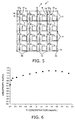
- FIG. 5 shows an equivalent circuit diagram of the basic configuration.
- the X-ray detector 1 is an indirect-type flat X-ray image detector.
- the X-ray detector 1 includes a photoelectric conversion substrate 2.
- the photoelectric conversion substrate 2 is an active matrix photoelectric conversion substrate for converting visible light to electrical signals.
- the photoelectric conversion substrate 2 includes a support substrate 3.
- the support substrate 3 is an insulating substrate formed from a translucent glass shaped like a rectangular plate.
- a plurality of pixels 4 are arranged with spacing from each other in a two-dimensional matrix.
- Each pixel 4 includes a thin film transistor (TFT) 5 as a switching element, a charge storage capacitor 6, a pixel electrode 7, and a photoelectric conversion element 8 such as a photodiode.
- TFT thin film transistor
- a plurality of control electrodes 11 are wired on the support substrate 3.
- the control electrode 11 is a control line along the row direction of the support substrate 3.
- the plurality of control electrodes 11 are each located between the pixels 4 on the support substrate 3 and spaced in the column direction of the support substrate 3.
- the gate electrodes 12 of the thin film transistors 5 are electrically connected to these control electrodes 11.
- a plurality of read electrodes 13 along the column direction of the support substrate 3 are wired on the support substrate 3.
- the plurality of read electrodes 13 are each located between the pixels 4 on the support substrate 3 and spaced in the row direction of the support substrate 3.
- the source electrodes 14 of the thin film transistors 5 are electrically connected to these read electrodes 13.
- the drain electrode 15 of the thin film transistor 5 is electrically connected to each of the charge storage capacitor 6 and the pixel electrode 7.
- the gate electrode 12 of the thin film transistor 5 is formed like an island on the support substrate 3.
- An insulating film 21 is stacked on the support substrate 3 including the gate electrode 12.
- the insulating film 21 covers each gate electrode 12.
- a plurality of island-shaped semi-insulating films 22 are stacked on the insulating film 21.
- the semi-insulating film 22 is formed from semiconductor and functions as a channel region of the thin film transistors 5.
- the semi-insulating films 22 are opposed to the respective gate electrodes 12 and cover these gate electrodes 12. That is, the semi-insulating films 22 are provided on the respective gate electrodes 12 via the insulating film 21.
- the source electrode 14 and the drain electrode 15 are each formed like an island on the insulating film 21 including the semi-insulating films 22.
- the source electrode 14 and the drain electrode 15 are insulated from and not electrically connected to each other.
- the source electrode 14 and the drain electrode 15 are provided on opposite sides on the gate electrode 12.
- One end part of the source electrode 14 and the drain electrode 15 is stacked on the semi-insulating film 22.
- the gate electrode 12 of each thin film transistor 5 is electrically connected to a common control electrode 11 together with the gate electrodes 12 of the other thin film transistors 5 located on the same row. Furthermore, the source electrode 14 of each thin film transistor 5 is electrically connected to a common read electrode 13 together with the source electrodes 14 of the other thin film transistors 5 located on the same column.
- the charge storage capacitor 6 includes an island-shaped lower electrode 23 formed on the support substrate 3.
- the insulating film 21 is stacked on the support substrate 3 including the lower electrode 23.
- the insulating film 21 extends from above the gate electrodes 12 of the thin film transistors 5 to above the lower electrodes 23.
- an island-shaped upper electrode 24 is stacked on the insulating film 21.
- the upper electrode 24 is opposed to the lower electrode 23 and covers the lower electrode 23. That is, the upper electrode 24 is provided on each lower electrode 23 via the insulating film 21.
- the drain electrode 15 is stacked on the insulating film 21 including the upper electrode 24. The other end part of the drain electrode 15 is stacked on the upper electrode 24 and electrically connected to the upper electrode 24.
- An insulating layer 25 is stacked on the insulating film 21 including the semi-insulating films 22, the source electrodes 14, and the drain electrodes 15 of the thin film transistors 5 and the upper electrodes 24 of the charge storage capacitors 6.
- the insulating layer 25 is formed from e.g. silicon oxide (SiO2) around each pixel electrode 7.
- a through hole 26 is opened in part of the insulating layer 25.
- the through hole 26 is a contact hole communicating with the drain electrode 15 of the thin film transistor 5.
- An island-shaped pixel electrode 7 is stacked on the insulating layer 25 including the through hole 26. The pixel electrode 7 is electrically connected to the drain electrode 15 of the thin film transistor 5 through the through hole 26.
- a photoelectric conversion element 8 such as a photodiode for converting visible light to electrical signals is stacked on each pixel electrode 7.
- a scintillator layer 31 is formed on the surface of the photoelectric conversion substrate 2 where the photoelectric conversion element 8 is formed.
- the scintillator layer 31 converts radiation such as X-rays to visible light.
- the scintillator layer 31 is formed by depositing a high-brightness fluorescent material in a columnar shape on the photoelectric conversion substrate 2 by vapor phase growth technique such as vacuum evaporation technique, sputtering technique, and CVD technique.
- the high-brightness fluorescent material is a phosphor such as a halide including cesium iodide (CsI) and an oxide-based compound including gadolinium oxysulfide (GOS).
- the scintillator layer 31 is formed to have a columnar crystal structure such that a plurality of strip-shaped columnar crystals 32 are formed in the in-plane direction of the photoelectric conversion substrate 2.
- a reflective layer 41 is stacked on the scintillator layer 31.
- the reflective layer 41 enhances the utilization efficiency of visible light converted in the scintillator layer 31.
- a protective layer 42 is stacked on the reflective layer 41.
- the protective layer 42 protects the scintillator layer 31 from moisture in the atmosphere.
- An insulating layer 43 is stacked on the protective layer 42.
- An X-ray grid 44 is formed on the insulating layer 43.
- the X-ray grid 44 is shaped like a grid for shielding between the pixels 4.
- the X-ray detector 1 In the X-ray detector 1 thus configured, radiation such as X-rays 51 is incident on the scintillator layer 31 and converted to visible light 52 in the columnar crystal 32 of the scintillator layer 31.
- the visible light 52 travels through the columnar crystal 32 to the photoelectric conversion element 8 of the photoelectric conversion substrate 2 and is converted to electrical signals.
- the electrical signal converted in the photoelectric conversion element 8 flows to the pixel electrode 7.
- the electrical signal is carried to the charge storage capacitor 6 connected to the pixel electrode 7.
- the electrical signal is held and stored in the charge storage capacitor 6 until the gate electrode 12 of the thin film transistor 5 connected to the pixel electrode 7 turns to the driving state.
- FIG. 2 a second structure example of the X-ray detector 1 is described with reference to FIG. 2 .
- the description uses the same reference numerals as in the first structure example of the X-ray detector 1, and omits the description of similar configurations and operations.
- the photoelectric conversion substrate 2 has the same structure and operation as that of the first structure example.
- a scintillator panel 62 is bonded onto the photoelectric conversion substrate 2 via a bonding layer 61.
- the scintillator panel 62 includes a support substrate 63 transmissive to X-rays 51.
- a reflective layer 41 reflective to light is formed on the support substrate 63.
- a scintillator layer 31 including a plurality of strip-shaped columnar crystals 32 is formed on the reflective layer 41.
- a protective layer 42 for sealing the scintillator layer 31 is stacked on the scintillator layer 31.
- an X-ray grid 44 shaped like a grid for shielding between the pixels 4 is formed on the support substrate 63.
- X-rays 51 are incident on the scintillator layer 31 of the scintillator panel 62 and converted to visible light 52 in the columnar crystal 32 of the scintillator layer 31.
- the visible light 52 travels through the columnar crystal 32 to the photoelectric conversion element 8 of the photoelectric conversion substrate 2 and is converted to electrical signals.
- the electrical signal is converted to a digital image signal for output as described above.
- the third structure example of the X-ray detector 1 is similar in configuration to the first structure example of the X-ray detector 1 shown in FIG. 1 except that the scintillator layer 31 does not include the columnar crystals 32.
- the fourth structure example of the X-ray detector 1 is similar in configuration to the second structure example of the X-ray detector 1 shown in FIG. 2 except that the scintillator layer 31 does not include the columnar crystals 32.
- the scintillator layer 31 is made of a phosphor containing Tl as an activator in CsI, which is a halide. Furthermore, the scintillator layer 31 has the following features (1), (2), and (3).
- the concentration of the activator in the phosphor is 1.6 mass% ⁇ 0.4 mass%.
- the concentration distribution of the activator in the in-plane direction and film thickness direction of the phosphor is within ⁇ 15%.
- the concentration distribution of the activator in the in-plane direction and film thickness direction of the phosphor is within ⁇ 15%. Thus, the uniformity is maintained.
- the scintillator layer 31 is formed by vacuum evaporation technique using two evaporation sources of CsI and TlI. Furthermore, preferably, the scintillator layer 31 has a structure of strip-shaped columnar crystals 32.
- the correlation of the Tl concentration in the scintillator layer 31 with various characteristics was tested. The result is shown in FIG. 6 to FIG. 8 .
- the film thickness of the scintillator layer 31 is 600 ⁇ m, and the activator is Tl.
- the correlation of the stacking pitch (formation pitch of a unit film thickness (formation film thickness per rotation of the substrate)) of the scintillator layer 31 with various characteristics was tested. The result is shown in FIG. 9 to FIG. 11 .
- FIG. 6 shows the correlation of the Tl concentration in the scintillator layer 31 with sensitivity ratio.
- the test condition is such that X-rays are incident at 70 kV and 0.0087 mGy.
- the sensitivity ratio is the ratio with reference to the sensitivity in the case where the Tl concentration in the scintillator layer 31 is 0.1 mass%.
- the condition for forming the scintillator layer of each test sample is the same (except the Tl concentration in the scintillator layer 31). As shown in FIG. 6 , the sensitivity was maximized for the Tl concentration in the scintillator layer 31 around 1.4 mass%-1.8 mass%.
- FIG. 7 shows the correlation of the Tl concentration in the scintillator layer 31 with MTF ratio.
- the MTF ratio represents resolution.
- the test condition is such that X-rays are incident at 70 kV and 0.0087 mGy.
- the MTF ratio is the ratio with reference to MTF (at 2 Lp/mm) in the case where the Tl concentration in the scintillator layer 31 is 0.1 mass%.
- the condition for forming the scintillator layer of each test sample is the same (except the Tl concentration in the scintillator layer 31). As shown in FIG. 7 , the result was generally constant up to the Tl concentration in the scintillator layer 31 around 2.0 mass%.
- FIG. 8 shows the correlation of the Tl concentration in the scintillator layer 31 with residual image ratio.
- the test condition is as follows.
- the dose of incident X-rays in the (n-1)-th X-ray image is greater than that in the n-th X-ray image.
- X-rays are incident at 70 kV and 0.87 mGy.
- the subject is a lead plate (plate thickness 3 mm).
- the X-ray image capture interval is 60 sec.
- X-rays are incident at 70 kV and 0.0087 mGy.
- the subject is none.
- the X-ray image capture interval is 60 sec.
- the residual image ratio is the ratio with reference to the residual image in the case where the Tl concentration in the scintillator layer 31 is 0.1 mass%.
- the condition for forming the scintillator layer of each test sample is the same (except the Tl concentration in the scintillator layer 31).
- the residual image was minimized for the Tl concentration in the scintillator layer 31 around 1.6 mass%.
- no residual image was observed in the region where the residual image ratio is 0.5 (preferably 0.4) or less and the Tl concentration in the scintillator layer 31 is 1.6 mass% ⁇ 0.4 mass%.
- FIG. 9 shows the correlation of the stacking pitch of the scintillator layer 31 with sensitivity ratio.
- the test condition is such that X-rays are incident at 70 kV and 0.0087 mGy.
- the Tl concentration in the scintillator layer 31 is 0.1 mass%.
- the sensitivity ratio is the ratio with reference to the sensitivity in the case where the stacking pitch of the scintillator layer 31 is 200 nm.
- the condition for forming the scintillator layer of each test sample is the same (except the Tl concentration in the scintillator layer 31).
- FIG. 10 shows the correlation of the stacking pitch of the scintillator layer 31 with MTF ratio.
- the test condition is such that X-rays are incident at 70 kV and 0.0087 mGy.
- the Tl concentration in the scintillator layer 31 is 0.1 mass%.
- the MTF ratio is the ratio with reference to MTF (at 2 Lp/mm) in the case where the stacking pitch of the scintillator layer 31 is 200 nm.
- the condition for forming the scintillator layer of each test sample is the same (except the Tl concentration in the scintillator layer 31).
- FIG. 11 shows the correlation of the stacking pitch of the scintillator layer 31 with residual image ratio.
- the test condition is such that the dose of incident X-rays in the (n-1)-th X-ray image is greater than that in the n-th X-ray image.
- X-rays are incident at 70 kV and 0.87 mGy.
- the subject is a lead plate (plate thickness 3 mm).
- the X-ray image capture interval is 60 sec.
- X-rays are incident at 70 kV and 0.0087 mGy.
- the subject is none.
- the X-ray image capture interval is 60 sec.
- the Tl concentration in the scintillator layer 31 is 0.1 mass%.
- the residual image ratio is the ratio with reference to the residual image in the case where the stacking pitch of the scintillator layer 31 is 200 nm.
- the condition for forming the scintillator layer of each test sample is the same (except the Tl concentration in the scintillator layer 31).
- the characteristics tend to be degraded in the region where the stacking pitch of the scintillator layer 31 is 200 nm or more.
- the light emission wavelength of the scintillator layer 31 has a peak wavelength around 550 nm.
- the scintillator layer 31 is made primarily of CsI, which has a refractive index of 1.8.
- the peak wavelength of light emission propagating in the scintillator layer 31 is denoted by ⁇ 1.
- the concentration of the activator in the phosphor constituting the scintillator layer 31 is around 1.6 mass%.
- No residual image was observed in the region of 1.6 mass% ⁇ 0.4 mass% where the residual image ratio is 0.5 (preferably 0.4) or less.
- the characteristics of sensitivity and MTF are also favorable in the region of 1.6 mass% ⁇ 0.4 mass%.
- the concentration of the activator is preferably in the region of 1.6 mass% ⁇ 0.4 mass%.
- the characteristics are nearly stable in the region where the Tl concentration in the scintillator layer 31 is 1.6 mass% ⁇ 0.4 mass%.
- the variation of the characteristics is small even if the Tl concentration in the scintillator layer 31 is varied (approximately ⁇ 15%).
- the concentration of the activator in the phosphor is in the region of 1.6 mass% ⁇ 0.4 mass%, the characteristics are likely to vary significantly if the concentration distribution of the activator is significantly biased in the in-plane direction and film thickness direction of the phosphor.
- the concentration distribution of the activator in the in-plane direction and film thickness direction of the phosphor is preferably within ⁇ 15%. The variation of characteristics is small and has little influence if the concentration distribution of the activator is in the variation range of approximately ⁇ 15%.
- the concentration of the activator in the phosphor is 1.6 mass% ⁇ 0.4 mass%, and the concentration distribution of the activator in the in-plane direction and film thickness direction of the phosphor is within ⁇ 15%.
- the characteristics are likely to vary significantly if the concentration distribution of the activator is significantly biased in the in-plane direction and film thickness direction of the phosphor.
- the concentration distribution of the activator in the in-plane direction and film thickness direction of the phosphor is within ⁇ 15%.
- FIG. 12 is a schematic view of a method for forming the scintillator layer 31.
- a substrate 72 (corresponding to the photoelectric conversion substrate 2 or the support substrate 63) is placed in the vacuum chamber 71.
- the film of the scintillator layer 31 is stacked by vacuum evaporation technique.
- evaporation particles from the evaporation source 73 of CsI and evaporation particles from the evaporation source 74 of TlI placed in the vacuum chamber 71 are evaporated on the stacking surface of the substrate 72 while rotating the substrate 72.
- the Tl concentration distribution in the in-plane direction and film thickness direction per stacking cycle of the scintillator layer 31 can be arbitrarily controlled by controlling the rotation cycle of the substrate 72 and the evaporation of CsI and TlI.
- the uniformity of the Tl concentration distribution in the in-plane direction and film thickness direction of the overall scintillator layer 31 is ensured by ensuring the uniformity of the Tl concentration distribution in the in-plane direction and film thickness direction per stacking cycle of the scintillator layer 31 when the scintillator layer 31 is formed.
- the characteristics, in particular the residual image characteristic, of the scintillator layer 31 can be improved by providing the above features (1)-(3) to the scintillator layer 31 made of a phosphor containing Tl as an activator in CsI, which is a halide.
- the film thickness of the scintillator layer 31 is 600 ⁇ m.
- the stacking pitch of the scintillator layer 31 is 150 nm.
- the concentration distribution of the activator in the in-plane direction and film thickness direction of the scintillator layer 31 is ⁇ 15%.
- the activator is Tl. Five samples are produced with the concentration of the activator in the scintillator layer 31 being 0.1 mass%, 1.0 mass%, 1.2 mass%, 1.6 mass%, and 2.0 mass%.
- FIGS. 13A, 13B, 13C, 13D, and 13E show (n-th) X-ray images in this case.
- the table of FIG. 14 shows the result of the characteristics.
- the sensitivity ratio, the MTF ratio, and the residual image ratio are the values with reference to the case where the Tl concentration in the scintillator layer 31 is 0.1 mass%.
- the radiography condition is as follows.
- the dose of incident X-rays in the (n-1)-th X-ray image is greater than that in the n-th X-ray image.
- X-rays are incident at 70 kV and 0.87 mGy.
- the subject is a lead plate (plate thickness 3 mm).
- the X-ray image capture interval is 60 sec.
- X-rays are incident at 70 kV and 0.0087 mGy.
- the subject is none.
- the X-ray image capture interval is 60 sec.
- the window processing is applied (the histogram average of the image ⁇ 10%).
- FIGS. 13A and 13B when the concentration of the activator is 0.1 mass% and 1.0 mass%, a residual image is observed in the range enclosed with the dashed line in the figure. As shown in FIGS. 13C, 13D, and 13E , when the concentration of the activator is 1.2 mass%, 1.6 mass%, and 2.0 mass%, no residual image is observed in the range enclosed with the dashed line in the figure.
- the residual image characteristic can be improved with the sensitivity and MTF being also favorable. This can improve the performance and reliability of the X-ray detector 1.
- FIG. 15 to FIG. 19 the basic configuration of the scintillator panel 90 is described with reference to first to fourth structure examples.
- the scintillator panel 90 includes a support substrate 91 transmissive to radiation such as X-rays.
- a reflective layer 92 reflective to light is formed on the support substrate 91.
- a scintillator layer 93 for converting radiation to visible light is formed on the reflective layer 92.
- a protective layer 94 for sealing the scintillator layer 93 is stacked on the scintillator layer 93.
- the support substrate 91 is formed from a material composed primarily of light elements rather than transition metal elements and having good X-ray transmittance.
- the reflective layer 92 is made of a metal material having high reflectance such as Al, Ni, Cu, Pd, and Ag.
- the reflective layer 92 reflects light generated in the scintillator layer 93 to the direction opposite to the support substrate 91.
- the reflective layer 92 enhances the light utilization efficiency.
- the scintillator layer 93 is formed by depositing a high-brightness fluorescent material in a columnar shape on the support substrate 91 by vapor phase growth technique such as vacuum evaporation technique, sputtering technique, and CVD technique.
- the high-brightness fluorescent material is a phosphor such as a halide including cesium iodide (CsI) and an oxide-based compound including gadolinium oxysulfide (GOS).
- CsI cesium iodide
- GOS gadolinium oxysulfide
- the scintillator layer 93 is formed in a columnar crystal structure such that a plurality of strip-shaped columnar crystals 93a are formed in the in-plane direction of the support substrate 91.
- the scintillator panel 90 thus configured, radiation such as X-rays 96 is incident on the scintillator layer 93 from the support substrate 91 side and converted to visible light 97 in the columnar crystal 93a of the scintillator layer 93.
- the visible light 97 is emitted from the surface of the scintillator layer 93 (the surface of the protective layer 94) on the opposite side from the support substrate 91.
- FIG. 16 shows a second structure example of the scintillator panel 90.
- the second structure example of the scintillator panel 90 is similar in configuration to the first structure example of the scintillator panel 90 shown in FIG. 15 except for not including the reflective layer 92.
- FIG. 17 shows a third structure example of the scintillator panel 90.
- the third structure example of the scintillator panel 90 is similar in configuration to the first structure example of the scintillator panel 90 shown in FIG. 15 except that the scintillator layer 93 does not include the columnar crystals 93a.
- FIG. 18 shows a fourth structure example of the scintillator panel 90.
- the fourth structure example of the scintillator panel 90 is similar in configuration to the second structure example of the scintillator panel 90 shown in FIG. 16 except that the scintillator layer 93 does not include the columnar crystals 93a.
- FIG. 19 shows a radiography device 100 of e.g. the CCD-DR type based on the scintillator panel 90.
- the radiography device 100 includes a housing 101.
- the scintillator panel 90 is placed at one end of the housing 101.
- a specular reflective plate 102 and an optical lens 103 are placed inside the housing 101.
- a light receiving element 104 such as CCD is placed at the other end of the housing 101.
- X-rays 96 are radiated from the X-ray source (X-ray tube) 105 and incident on the scintillator panel 90.
- the visible light 97 converted in the scintillator layer 93 is emitted from the surface of the scintillator layer 93.
- the X-ray image is projected on the surface of the scintillator layer 93. This X-ray image is reflected by the reflective plate 102. On the other hand, the X-ray image is collected by the optical lens 103 and applied to the light receiving element 104. The X-ray image is converted to electrical signals in the light receiving element 104 for output.
- the scintillator layer 93 is made of a phosphor containing Tl as an activator in CsI, which is a halide. Furthermore, the scintillator layer 93 has the following features (1), (2), and (3).
- the concentration of the activator in the phosphor is 1.6 mass% ⁇ 0.4 mass%.
- the concentration distribution of the activator in the in-plane direction and film thickness direction of the phosphor is within ⁇ 15%.
- the concentration distribution of the activator in the in-plane direction and film thickness direction of the phosphor is within ⁇ 15%. Thus, the uniformity is maintained.
- the scintillator layer 93 is formed by vacuum evaporation technique using two evaporation sources of CsI and TlI. Furthermore, preferably, the scintillator layer 93 has a structure of strip-shaped columnar crystals 93a.
- the scintillator layer 93 having the above features (1)-(3) defined in this embodiment is used in the scintillator panel 90.
- the residual image characteristic can be improved with favorable sensitivity and MTF provided to the scintillator panel 90. This can improve the performance and reliability of the scintillator panel 90.
- the method for forming the scintillator layer 93 can be made similar to the method for forming the scintillator layer 31 described with reference to FIG. 12 .
Landscapes
- Chemical & Material Sciences (AREA)
- Engineering & Computer Science (AREA)
- Materials Engineering (AREA)
- Organic Chemistry (AREA)
- Crystallography & Structural Chemistry (AREA)
- Metallurgy (AREA)
- General Physics & Mathematics (AREA)
- Life Sciences & Earth Sciences (AREA)
- Health & Medical Sciences (AREA)
- High Energy & Nuclear Physics (AREA)
- Molecular Biology (AREA)
- Spectroscopy & Molecular Physics (AREA)
- Physics & Mathematics (AREA)
- Chemical Kinetics & Catalysis (AREA)
- Inorganic Chemistry (AREA)
- General Chemical & Material Sciences (AREA)
- Mechanical Engineering (AREA)
- Measurement Of Radiation (AREA)
Abstract
Description
- This invention generally relates to a radiation detector, a scintillator panel, and a method for manufacturing the same.
- An X-ray detector can be realized as a flat radiation detector based on solid-state imaging elements such as active matrix, CCD, and CMOS. Such an X-ray detector is drawing attention as a new-generation X-ray image detector for diagnosis. A radiographic image or real-time X-ray image is outputted as digital signals by irradiating this X-ray detector with X-rays.
- The X-ray detector includes a photoelectric conversion substrate for converting light to electrical signals, and a scintillator layer in contact with the photoelectric conversion substrate. The scintillator layer converts externally incident X-rays to light. The light converted from incident X-rays in the scintillator layer reaches the photoelectric conversion substrate and is converted to electric charge. This charge is read as an output signal and converted to digital image signals in e.g. a prescribed signal processing circuit.
- The scintillator layer may be made of CsI, which is a halide. In this case, incident X-rays cannot be converted to visible light by CsI alone. Thus, as in commonly-used phosphors, an activator is contained to activate excitation of light in response to incident X-rays.
- In the X-ray detector, the light reception sensitivity of the photoelectric conversion substrate has a peak wavelength around 400-700 nm in the visible range. Thus, in the case where the scintillator layer is made of CsI, Tl is used as an activator. Then, the light excited by incident X-rays has a wavelength around 550 nm.
- The scintillator layer may be made of a phosphor containing Tl as an activator in CsI, which is a halide. In this case, as in commonly-used phosphors containing an activator, the characteristics of the scintillator layer are significantly affected by the concentration and concentration distribution of Tl serving as an activator.
- In the X-ray detector including a scintillator layer containing an activator, lack of optimization of the concentration and concentration distribution of the activator incurs characteristics degradation of the scintillator layer. This affects the sensitivity (light emission efficiency) and residual image (the phenomenon in which the subject image of the X-ray image at the (n-1)-th or earlier time remains in the X-ray image at the n-th time) related to the light emission characteristics of the scintillator layer.
- For instance, in diagnosis using X-ray images, the radiography condition significantly varies with subjects (incident X-rays at a dose of approximately 0.0087-0.87 mGy, because the X-ray transmittance varies with body regions). This may cause a significant difference in the dose of incident X-rays between the (n-1)-th X-ray image and the n-th X-ray image. Here, if the dose of incident X-rays in the (n-1)-th X-ray image is greater than that in the n-th X-ray image, the light emission characteristics of the scintillator layer in the non-subject part of the (n-1)-th X-ray image is changed by the great energy of incident X-rays. This influence remains also in the n-th X-ray image and produces a residual image.
- In diagnosis using X-ray images, the residual image characteristic is more important than other characteristics of the scintillator layer such as sensitivity (light emission efficiency) and resolution (MTF).
- Conventionally, there have been proposals for defining the concentration and concentration distribution of the activator of the scintillator layer for the purpose of improving sensitivity (light emission efficiency) and resolution (MTF).
- [Patent Literature 1]
JP2008-51793 A - Conventional proposals for characteristics improvement of the scintillator layer largely relate to sensitivity (light emission efficiency) and resolution (MTF). There have been few proposals related to overall characteristics improvement including the residual image characteristic.
- The problem to be solved by the invention is to provide a radiation detector, a scintillator panel, and a method for manufacturing the same capable of improving overall characteristics including the residual image characteristic of the scintillator layer.
- According to the embodiment, a radiation detector includes a photoelectric conversion substrate converting light to an electrical signal and a scintillator layer being in contact with the photoelectric conversion substrate and converting externally incident radiation to light. The scintillator layer is made of a phosphor containing Tl as an activator in CsI, which is a halide. A concentration of the activator in the phosphor is 1.6 mass%±0.4 mass%, and a concentration distribution of the activator in an in-plane direction and a film thickness direction is within ±15%.
-
- [
FIG. 1] FIG. 1 is a sectional view of a first structure example of a radiation detector showing an embodiment. - [
FIG. 2] FIG. 2 is a sectional view of a second structure example of the above radiation detector. - [
FIG. 3] FIG. 3 is a sectional view of a third structure example of the above radiation detector. - [
FIG. 4] FIG. 4 is a sectional view of a fourth structure example of the above radiation detector. - [
FIG. 5] FIG. 5 is an equivalent circuit diagram of the above radiation detector. - [
FIG. 6] FIG. 6 is a graph showing the correlation between Tl concentration and sensitivity ratio of the scintillator layer of the above radiation detector. - [
FIG. 7] FIG. 7 is a graph showing the correlation between Tl concentration and MTF ratio of the above scintillator layer. - [
FIG. 8] FIG. 8 is a graph showing the correlation between Tl concentration and residual image ratio of the above scintillator layer. - [
FIG. 9] FIG. 9 is a graph showing the correlation between stacking pitch and sensitivity ratio of the above scintillator layer. - [
FIG. 10] FIG. 10 is a graph showing the correlation between stacking pitch and MTF ratio of the above scintillator layer. - [
FIG. 11] FIG. 11 is a graph showing the correlation between stacking pitch and residual image ratio of the above scintillator layer. - [
FIG. 12] FIG. 12 is a schematic view showing a method for forming the above scintillator layer. - [
FIG. 13] FIGS. 13A to 13E are X-ray images radiographed under particular radiography conditions by the above radiation detector.FIG. 13A is an X-ray image at a Tl concentration of 0.1 mass%.FIG. 13B is an X-ray image at a Tl concentration of 1.0 mass%.FIG. 13C is an X-ray image at a Tl concentration of 1.2 mass%.FIG. 13D is an X-ray image at a Tl concentration of 1.6 mass%.FIG. 13E is an X-ray image at a Tl concentration of 2.0 mass%. - [
FIG. 14] FIG. 14 is a table showing characteristics of the above radiation detector at a Tl concentration of 0.1 mass%, 1.0 mass%, 1.2 mass%, 1.6 mass%, and 2.0 mass%. - [
FIG. 15] FIG. 15 is a sectional view of a first structure example of a scintillator panel showing an embodiment. - [
FIG. 16] FIG. 16 is a sectional view of a second structure example of the above scintillator panel. - [
FIG. 17] FIG. 17 is a sectional view of a third structure example of the above scintillator panel. - [
FIG. 18] FIG. 18 is a sectional view of a fourth structure example of the above scintillator panel. - [
FIG. 19] FIG. 19 is a sectional view of a radiography device based on the above scintillator panel. - Embodiments according to the invention are now described with reference to
FIG. 1 to FIG. 19 . - In
FIG. 1 to FIG. 4 , the basic configuration of aradiation detector 1 is described with reference to first to fourth structure examples.FIG. 5 shows an equivalent circuit diagram of the basic configuration. - First, a first structure example of the
X-ray detector 1 as a radiation detector is described with reference toFIG. 1 andFIG. 5 . As shown inFIG. 1 , theX-ray detector 1 is an indirect-type flat X-ray image detector. TheX-ray detector 1 includes aphotoelectric conversion substrate 2. Thephotoelectric conversion substrate 2 is an active matrix photoelectric conversion substrate for converting visible light to electrical signals. - The
photoelectric conversion substrate 2 includes asupport substrate 3. Thesupport substrate 3 is an insulating substrate formed from a translucent glass shaped like a rectangular plate. On the surface of thesupport substrate 3, a plurality ofpixels 4 are arranged with spacing from each other in a two-dimensional matrix. Eachpixel 4 includes a thin film transistor (TFT) 5 as a switching element, acharge storage capacitor 6, apixel electrode 7, and aphotoelectric conversion element 8 such as a photodiode. - As shown in
FIG. 5 , a plurality ofcontrol electrodes 11 are wired on thesupport substrate 3. Thecontrol electrode 11 is a control line along the row direction of thesupport substrate 3. The plurality ofcontrol electrodes 11 are each located between thepixels 4 on thesupport substrate 3 and spaced in the column direction of thesupport substrate 3. Thegate electrodes 12 of thethin film transistors 5 are electrically connected to thesecontrol electrodes 11. - A plurality of read
electrodes 13 along the column direction of thesupport substrate 3 are wired on thesupport substrate 3. The plurality of readelectrodes 13 are each located between thepixels 4 on thesupport substrate 3 and spaced in the row direction of thesupport substrate 3. Thesource electrodes 14 of thethin film transistors 5 are electrically connected to these readelectrodes 13. Thedrain electrode 15 of thethin film transistor 5 is electrically connected to each of thecharge storage capacitor 6 and thepixel electrode 7. - As shown in
FIG. 1 , thegate electrode 12 of thethin film transistor 5 is formed like an island on thesupport substrate 3. An insulatingfilm 21 is stacked on thesupport substrate 3 including thegate electrode 12. The insulatingfilm 21 covers eachgate electrode 12. A plurality of island-shapedsemi-insulating films 22 are stacked on the insulatingfilm 21. Thesemi-insulating film 22 is formed from semiconductor and functions as a channel region of thethin film transistors 5. Thesemi-insulating films 22 are opposed to therespective gate electrodes 12 and cover thesegate electrodes 12. That is, thesemi-insulating films 22 are provided on therespective gate electrodes 12 via the insulatingfilm 21. - The
source electrode 14 and thedrain electrode 15 are each formed like an island on the insulatingfilm 21 including thesemi-insulating films 22. Thesource electrode 14 and thedrain electrode 15 are insulated from and not electrically connected to each other. Thesource electrode 14 and thedrain electrode 15 are provided on opposite sides on thegate electrode 12. One end part of thesource electrode 14 and thedrain electrode 15 is stacked on thesemi-insulating film 22. - As shown in
FIG. 5 , thegate electrode 12 of eachthin film transistor 5 is electrically connected to acommon control electrode 11 together with thegate electrodes 12 of the otherthin film transistors 5 located on the same row. Furthermore, thesource electrode 14 of eachthin film transistor 5 is electrically connected to acommon read electrode 13 together with thesource electrodes 14 of the otherthin film transistors 5 located on the same column. - As shown in
FIG. 1 , thecharge storage capacitor 6 includes an island-shapedlower electrode 23 formed on thesupport substrate 3. The insulatingfilm 21 is stacked on thesupport substrate 3 including thelower electrode 23. The insulatingfilm 21 extends from above thegate electrodes 12 of thethin film transistors 5 to above thelower electrodes 23. Furthermore, an island-shapedupper electrode 24 is stacked on the insulatingfilm 21. Theupper electrode 24 is opposed to thelower electrode 23 and covers thelower electrode 23. That is, theupper electrode 24 is provided on eachlower electrode 23 via the insulatingfilm 21. Thedrain electrode 15 is stacked on the insulatingfilm 21 including theupper electrode 24. The other end part of thedrain electrode 15 is stacked on theupper electrode 24 and electrically connected to theupper electrode 24. - An insulating
layer 25 is stacked on the insulatingfilm 21 including thesemi-insulating films 22, thesource electrodes 14, and thedrain electrodes 15 of thethin film transistors 5 and theupper electrodes 24 of thecharge storage capacitors 6. The insulatinglayer 25 is formed from e.g. silicon oxide (SiO2) around eachpixel electrode 7. - A through
hole 26 is opened in part of the insulatinglayer 25. The throughhole 26 is a contact hole communicating with thedrain electrode 15 of thethin film transistor 5. An island-shapedpixel electrode 7 is stacked on the insulatinglayer 25 including the throughhole 26. Thepixel electrode 7 is electrically connected to thedrain electrode 15 of thethin film transistor 5 through the throughhole 26. - A
photoelectric conversion element 8 such as a photodiode for converting visible light to electrical signals is stacked on eachpixel electrode 7. - A
scintillator layer 31 is formed on the surface of thephotoelectric conversion substrate 2 where thephotoelectric conversion element 8 is formed. Thescintillator layer 31 converts radiation such as X-rays to visible light. Thescintillator layer 31 is formed by depositing a high-brightness fluorescent material in a columnar shape on thephotoelectric conversion substrate 2 by vapor phase growth technique such as vacuum evaporation technique, sputtering technique, and CVD technique. The high-brightness fluorescent material is a phosphor such as a halide including cesium iodide (CsI) and an oxide-based compound including gadolinium oxysulfide (GOS). Thescintillator layer 31 is formed to have a columnar crystal structure such that a plurality of strip-shapedcolumnar crystals 32 are formed in the in-plane direction of thephotoelectric conversion substrate 2. - A
reflective layer 41 is stacked on thescintillator layer 31. Thereflective layer 41 enhances the utilization efficiency of visible light converted in thescintillator layer 31. Aprotective layer 42 is stacked on thereflective layer 41. Theprotective layer 42 protects thescintillator layer 31 from moisture in the atmosphere. An insulatinglayer 43 is stacked on theprotective layer 42. AnX-ray grid 44 is formed on the insulatinglayer 43. TheX-ray grid 44 is shaped like a grid for shielding between thepixels 4. - In the
X-ray detector 1 thus configured, radiation such asX-rays 51 is incident on thescintillator layer 31 and converted tovisible light 52 in thecolumnar crystal 32 of thescintillator layer 31. - The
visible light 52 travels through thecolumnar crystal 32 to thephotoelectric conversion element 8 of thephotoelectric conversion substrate 2 and is converted to electrical signals. The electrical signal converted in thephotoelectric conversion element 8 flows to thepixel electrode 7. The electrical signal is carried to thecharge storage capacitor 6 connected to thepixel electrode 7. The electrical signal is held and stored in thecharge storage capacitor 6 until thegate electrode 12 of thethin film transistor 5 connected to thepixel electrode 7 turns to the driving state. - At this time, when one of the
control electrodes 11 is turned to the driving state, one row ofthin film transistors 5 connected to thiscontrol electrode 11 turned to the driving state turn to the driving state. - The electrical signal stored in the
charge storage capacitor 6 connected to eachthin film transistor 5 turned to the driving state is outputted to theread electrode 13. - This results in outputting a signal corresponding to a particular row of
pixels 4 of the X-ray image. Thus, the signal corresponding to all thepixels 4 of the X-ray image can be outputted by the driving control of thecontrol electrodes 11. This output signal is converted to a digital image signal for output. - Next, a second structure example of the
X-ray detector 1 is described with reference toFIG. 2 . The description uses the same reference numerals as in the first structure example of theX-ray detector 1, and omits the description of similar configurations and operations. - The
photoelectric conversion substrate 2 has the same structure and operation as that of the first structure example. - A
scintillator panel 62 is bonded onto thephotoelectric conversion substrate 2 via abonding layer 61. Thescintillator panel 62 includes asupport substrate 63 transmissive toX-rays 51. Areflective layer 41 reflective to light is formed on thesupport substrate 63. Ascintillator layer 31 including a plurality of strip-shapedcolumnar crystals 32 is formed on thereflective layer 41. Aprotective layer 42 for sealing thescintillator layer 31 is stacked on thescintillator layer 31. Furthermore, anX-ray grid 44 shaped like a grid for shielding between thepixels 4 is formed on thesupport substrate 63. - In the
X-ray detector 1 thus configured,X-rays 51 are incident on thescintillator layer 31 of thescintillator panel 62 and converted tovisible light 52 in thecolumnar crystal 32 of thescintillator layer 31. - The
visible light 52 travels through thecolumnar crystal 32 to thephotoelectric conversion element 8 of thephotoelectric conversion substrate 2 and is converted to electrical signals. The electrical signal is converted to a digital image signal for output as described above. - Next, a third structure example of the
X-ray detector 1 is described with reference toFIG. 3 . The third structure example of theX-ray detector 1 is similar in configuration to the first structure example of theX-ray detector 1 shown inFIG. 1 except that thescintillator layer 31 does not include thecolumnar crystals 32. - Next, a fourth structure example of the
X-ray detector 1 is described with reference toFIG. 4 . The fourth structure example of theX-ray detector 1 is similar in configuration to the second structure example of theX-ray detector 1 shown inFIG. 2 except that thescintillator layer 31 does not include thecolumnar crystals 32. - In the
X-ray detector 1 of the structures shown inFIG. 1 to FIG. 4 , thescintillator layer 31 is made of a phosphor containing Tl as an activator in CsI, which is a halide. Furthermore, thescintillator layer 31 has the following features (1), (2), and (3). - (1) The concentration of the activator in the phosphor is 1.6 mass%±0.4 mass%. The concentration distribution of the activator in the in-plane direction and film thickness direction of the phosphor is within ±15%.
- (2) In at least the region of a unit film thickness of 200 nm or less, the concentration distribution of the activator in the in-plane direction and film thickness direction of the phosphor is within ±15%. Thus, the uniformity is maintained.
- (3) The
scintillator layer 31 is formed by vacuum evaporation technique using two evaporation sources of CsI and TlI. Furthermore, preferably, thescintillator layer 31 has a structure of strip-shapedcolumnar crystals 32. - In the
X-ray detector 1 of the first structure example shown inFIG. 1 , the correlation of the Tl concentration in thescintillator layer 31 with various characteristics was tested. The result is shown inFIG. 6 to FIG. 8 . In this test, the film thickness of thescintillator layer 31 is 600 µm, and the activator is Tl. Furthermore, the correlation of the stacking pitch (formation pitch of a unit film thickness (formation film thickness per rotation of the substrate)) of thescintillator layer 31 with various characteristics was tested. The result is shown inFIG. 9 to FIG. 11 . -
FIG. 6 shows the correlation of the Tl concentration in thescintillator layer 31 with sensitivity ratio. The test condition is such that X-rays are incident at 70 kV and 0.0087 mGy. The sensitivity ratio is the ratio with reference to the sensitivity in the case where the Tl concentration in thescintillator layer 31 is 0.1 mass%. The condition for forming the scintillator layer of each test sample is the same (except the Tl concentration in the scintillator layer 31). As shown inFIG. 6 , the sensitivity was maximized for the Tl concentration in thescintillator layer 31 around 1.4 mass%-1.8 mass%. -
FIG. 7 shows the correlation of the Tl concentration in thescintillator layer 31 with MTF ratio. The MTF ratio represents resolution. The test condition is such that X-rays are incident at 70 kV and 0.0087 mGy. The MTF ratio is the ratio with reference to MTF (at 2 Lp/mm) in the case where the Tl concentration in thescintillator layer 31 is 0.1 mass%. The condition for forming the scintillator layer of each test sample is the same (except the Tl concentration in the scintillator layer 31). As shown inFIG. 7 , the result was generally constant up to the Tl concentration in thescintillator layer 31 around 2.0 mass%. -
FIG. 8 shows the correlation of the Tl concentration in thescintillator layer 31 with residual image ratio. The test condition is as follows. The dose of incident X-rays in the (n-1)-th X-ray image is greater than that in the n-th X-ray image. In the (n-1)-th X-ray image, X-rays are incident at 70 kV and 0.87 mGy. The subject is a lead plate (plate thickness 3 mm). The X-ray image capture interval is 60 sec. In the n-th X-ray image, X-rays are incident at 70 kV and 0.0087 mGy. The subject is none. The X-ray image capture interval is 60 sec. Furthermore, the residual image ratio is the ratio with reference to the residual image in the case where the Tl concentration in thescintillator layer 31 is 0.1 mass%. The condition for forming the scintillator layer of each test sample is the same (except the Tl concentration in the scintillator layer 31). As shown inFIG. 8 , the residual image was minimized for the Tl concentration in thescintillator layer 31 around 1.6 mass%. Furthermore, no residual image was observed in the region where the residual image ratio is 0.5 (preferably 0.4) or less and the Tl concentration in thescintillator layer 31 is 1.6 mass%±0.4 mass%. -
FIG. 9 shows the correlation of the stacking pitch of thescintillator layer 31 with sensitivity ratio. The test condition is such that X-rays are incident at 70 kV and 0.0087 mGy. The Tl concentration in thescintillator layer 31 is 0.1 mass%. The sensitivity ratio is the ratio with reference to the sensitivity in the case where the stacking pitch of thescintillator layer 31 is 200 nm. The condition for forming the scintillator layer of each test sample is the same (except the Tl concentration in the scintillator layer 31). -
FIG. 10 shows the correlation of the stacking pitch of thescintillator layer 31 with MTF ratio. The test condition is such that X-rays are incident at 70 kV and 0.0087 mGy. The Tl concentration in thescintillator layer 31 is 0.1 mass%. The MTF ratio is the ratio with reference to MTF (at 2 Lp/mm) in the case where the stacking pitch of thescintillator layer 31 is 200 nm. The condition for forming the scintillator layer of each test sample is the same (except the Tl concentration in the scintillator layer 31). -
FIG. 11 shows the correlation of the stacking pitch of thescintillator layer 31 with residual image ratio. The test condition is such that the dose of incident X-rays in the (n-1)-th X-ray image is greater than that in the n-th X-ray image. In the (n-1)-th X-ray image, X-rays are incident at 70 kV and 0.87 mGy. The subject is a lead plate (plate thickness 3 mm). The X-ray image capture interval is 60 sec. In the n-th X-ray image, X-rays are incident at 70 kV and 0.0087 mGy. The subject is none. The X-ray image capture interval is 60 sec. Furthermore, the Tl concentration in thescintillator layer 31 is 0.1 mass%. The residual image ratio is the ratio with reference to the residual image in the case where the stacking pitch of thescintillator layer 31 is 200 nm. The condition for forming the scintillator layer of each test sample is the same (except the Tl concentration in the scintillator layer 31). - As shown in
FIG. 9 to FIG. 11 , the characteristics tend to be degraded in the region where the stacking pitch of thescintillator layer 31 is 200 nm or more. - The light emission wavelength of the
scintillator layer 31 has a peak wavelength around 550 nm. Thescintillator layer 31 is made primarily of CsI, which has a refractive index of 1.8. The peak wavelength of light emission propagating in thescintillator layer 31 is denoted by λ1. Then, it can be regarded that λ1 = 550 nm/1.8 = 306 nm from the relationship between refractive index and wavelength. Thus, in the case where the stacking pitch of thescintillator layer 31 is larger than λ1, the result ofFIG. 9 to FIG. 11 is attributable to the increased possibility of the influence of the degradation of optical characteristics (such as scattering and attenuation) associated with e.g. variation of the crystallinity of thescintillator layer 31 and variation of the Tl concentration in thescintillator layer 31. - As shown in
FIG. 8 , the residual image was minimized when the concentration of the activator in the phosphor constituting thescintillator layer 31 is around 1.6 mass%. No residual image was observed in the region of 1.6 mass%±0.4 mass% where the residual image ratio is 0.5 (preferably 0.4) or less. Furthermore, as shown inFIG. 6 andFIG. 7 , the characteristics of sensitivity and MTF are also favorable in the region of 1.6 mass%±0.4 mass%. Thus, the concentration of the activator is preferably in the region of 1.6 mass%±0.4 mass%. - As shown in
FIG. 6 to FIG. 8 , the characteristics are nearly stable in the region where the Tl concentration in thescintillator layer 31 is 1.6 mass%±0.4 mass%. Thus, the variation of the characteristics is small even if the Tl concentration in thescintillator layer 31 is varied (approximately ±15%). - Even if the concentration of the activator in the phosphor is in the region of 1.6 mass% ±0.4 mass%, the characteristics are likely to vary significantly if the concentration distribution of the activator is significantly biased in the in-plane direction and film thickness direction of the phosphor. Thus, the concentration distribution of the activator in the in-plane direction and film thickness direction of the phosphor is preferably within ±15%. The variation of characteristics is small and has little influence if the concentration distribution of the activator is in the variation range of approximately ±15%.
- Thus, as described above in feature (1), preferably, the concentration of the activator in the phosphor is 1.6 mass%±0.4 mass%, and the concentration distribution of the activator in the in-plane direction and film thickness direction of the phosphor is within ±15%.
- In at least the region of the phosphor where the unit film thickness is 200 nm or less, the characteristics are likely to vary significantly if the concentration distribution of the activator is significantly biased in the in-plane direction and film thickness direction of the phosphor. Thus, as described above in feature (2), preferably, also in the region of a unit film thickness of 200 nm or less, the concentration distribution of the activator in the in-plane direction and film thickness direction of the phosphor is within ±15%.
-
FIG. 12 is a schematic view of a method for forming thescintillator layer 31. A substrate 72 (corresponding to thephotoelectric conversion substrate 2 or the support substrate 63) is placed in thevacuum chamber 71. The film of thescintillator layer 31 is stacked by vacuum evaporation technique. In the vacuum evaporation technique, evaporation particles from theevaporation source 73 of CsI and evaporation particles from the evaporation source 74 of TlI placed in thevacuum chamber 71 are evaporated on the stacking surface of thesubstrate 72 while rotating thesubstrate 72. - At this time, the Tl concentration distribution in the in-plane direction and film thickness direction per stacking cycle of the
scintillator layer 31 can be arbitrarily controlled by controlling the rotation cycle of thesubstrate 72 and the evaporation of CsI and TlI. Thus, the uniformity of the Tl concentration distribution in the in-plane direction and film thickness direction of theoverall scintillator layer 31 is ensured by ensuring the uniformity of the Tl concentration distribution in the in-plane direction and film thickness direction per stacking cycle of thescintillator layer 31 when thescintillator layer 31 is formed. - Accordingly, the characteristics, in particular the residual image characteristic, of the
scintillator layer 31 can be improved by providing the above features (1)-(3) to thescintillator layer 31 made of a phosphor containing Tl as an activator in CsI, which is a halide. - A practical example of the
X-ray detector 1 of the first structure example shown inFIG. 1 is now described. In this practical example, the film thickness of thescintillator layer 31 is 600 µm. The stacking pitch of thescintillator layer 31 is 150 nm. The concentration distribution of the activator in the in-plane direction and film thickness direction of thescintillator layer 31 is ±15%. The activator is Tl. Five samples are produced with the concentration of the activator in thescintillator layer 31 being 0.1 mass%, 1.0 mass%, 1.2 mass%, 1.6 mass%, and 2.0 mass%. - For these five samples, the subject is radiographed under a particular radiography condition. The radiographed image is processed in a prescribed image processing condition.
FIGS. 13A, 13B, 13C, 13D, and 13E show (n-th) X-ray images in this case. The table ofFIG. 14 shows the result of the characteristics. InFIG. 14 , the sensitivity ratio, the MTF ratio, and the residual image ratio are the values with reference to the case where the Tl concentration in thescintillator layer 31 is 0.1 mass%. - The radiography condition is as follows. The dose of incident X-rays in the (n-1)-th X-ray image is greater than that in the n-th X-ray image. In the (n-1)-th X-ray image, X-rays are incident at 70 kV and 0.87 mGy. The subject is a lead plate (
plate thickness 3 mm). The X-ray image capture interval is 60 sec. In the n-th X-ray image, X-rays are incident at 70 kV and 0.0087 mGy. The subject is none. The X-ray image capture interval is 60 sec. - With regard to the image processing condition, the flat field correction is applied. The window processing is applied (the histogram average of the image ± 10%).
- As shown in
FIGS. 13A and 13B , when the concentration of the activator is 0.1 mass% and 1.0 mass%, a residual image is observed in the range enclosed with the dashed line in the figure. As shown inFIGS. 13C, 13D, and 13E , when the concentration of the activator is 1.2 mass%, 1.6 mass%, and 2.0 mass%, no residual image is observed in the range enclosed with the dashed line in the figure. - Thus, if the above features (1)-(3) defined in this embodiment are provided to the
scintillator layer 31, the residual image characteristic can be improved with the sensitivity and MTF being also favorable. This can improve the performance and reliability of theX-ray detector 1. - Next, an embodiment in which the scintillator layer according to the invention is used in a scintillator panel is described.
- In
FIG. 15 to FIG. 19 , the basic configuration of thescintillator panel 90 is described with reference to first to fourth structure examples. - First, a first structure example of the
scintillator panel 90 is described with reference toFIG. 15 . Thescintillator panel 90 includes asupport substrate 91 transmissive to radiation such as X-rays. Areflective layer 92 reflective to light is formed on thesupport substrate 91. Ascintillator layer 93 for converting radiation to visible light is formed on thereflective layer 92. Aprotective layer 94 for sealing thescintillator layer 93 is stacked on thescintillator layer 93. - The
support substrate 91 is formed from a material composed primarily of light elements rather than transition metal elements and having good X-ray transmittance. - The
reflective layer 92 is made of a metal material having high reflectance such as Al, Ni, Cu, Pd, and Ag. Thereflective layer 92 reflects light generated in thescintillator layer 93 to the direction opposite to thesupport substrate 91. Thus, thereflective layer 92 enhances the light utilization efficiency. - The
scintillator layer 93 is formed by depositing a high-brightness fluorescent material in a columnar shape on thesupport substrate 91 by vapor phase growth technique such as vacuum evaporation technique, sputtering technique, and CVD technique. The high-brightness fluorescent material is a phosphor such as a halide including cesium iodide (CsI) and an oxide-based compound including gadolinium oxysulfide (GOS). Thescintillator layer 93 is formed in a columnar crystal structure such that a plurality of strip-shapedcolumnar crystals 93a are formed in the in-plane direction of thesupport substrate 91. - In the
scintillator panel 90 thus configured, radiation such asX-rays 96 is incident on thescintillator layer 93 from thesupport substrate 91 side and converted tovisible light 97 in thecolumnar crystal 93a of thescintillator layer 93. Thevisible light 97 is emitted from the surface of the scintillator layer 93 (the surface of the protective layer 94) on the opposite side from thesupport substrate 91. -
FIG. 16 shows a second structure example of thescintillator panel 90. The second structure example of thescintillator panel 90 is similar in configuration to the first structure example of thescintillator panel 90 shown inFIG. 15 except for not including thereflective layer 92. -
FIG. 17 shows a third structure example of thescintillator panel 90. The third structure example of thescintillator panel 90 is similar in configuration to the first structure example of thescintillator panel 90 shown inFIG. 15 except that thescintillator layer 93 does not include thecolumnar crystals 93a. -
FIG. 18 shows a fourth structure example of thescintillator panel 90. The fourth structure example of thescintillator panel 90 is similar in configuration to the second structure example of thescintillator panel 90 shown inFIG. 16 except that thescintillator layer 93 does not include thecolumnar crystals 93a. -
FIG. 19 shows aradiography device 100 of e.g. the CCD-DR type based on thescintillator panel 90. Theradiography device 100 includes ahousing 101. Thescintillator panel 90 is placed at one end of thehousing 101. A specularreflective plate 102 and anoptical lens 103 are placed inside thehousing 101. Alight receiving element 104 such as CCD is placed at the other end of thehousing 101.X-rays 96 are radiated from the X-ray source (X-ray tube) 105 and incident on thescintillator panel 90. Thevisible light 97 converted in thescintillator layer 93 is emitted from the surface of thescintillator layer 93. The X-ray image is projected on the surface of thescintillator layer 93. This X-ray image is reflected by thereflective plate 102. On the other hand, the X-ray image is collected by theoptical lens 103 and applied to thelight receiving element 104. The X-ray image is converted to electrical signals in thelight receiving element 104 for output. - In the
scintillator panel 90 of the structures shown inFIG. 15 to FIG. 19 , thescintillator layer 93 is made of a phosphor containing Tl as an activator in CsI, which is a halide. Furthermore, thescintillator layer 93 has the following features (1), (2), and (3). - (1) The concentration of the activator in the phosphor is 1.6 mass%±0.4 mass%. The concentration distribution of the activator in the in-plane direction and film thickness direction of the phosphor is within ±15%.
- (2) In at least the region of a unit film thickness of 200 nm or less, the concentration distribution of the activator in the in-plane direction and film thickness direction of the phosphor is within ±15%. Thus, the uniformity is maintained.
- (3) The
scintillator layer 93 is formed by vacuum evaporation technique using two evaporation sources of CsI and TlI. Furthermore, preferably, thescintillator layer 93 has a structure of strip-shapedcolumnar crystals 93a. - As described with reference to
FIG. 6 to FIG. 11 , thescintillator layer 93 having the above features (1)-(3) defined in this embodiment is used in thescintillator panel 90. Thus, the residual image characteristic can be improved with favorable sensitivity and MTF provided to thescintillator panel 90. This can improve the performance and reliability of thescintillator panel 90. - The method for forming the
scintillator layer 93 can be made similar to the method for forming thescintillator layer 31 described with reference toFIG. 12 . - While certain embodiments have been described, these embodiments have been presented by way of example only, and are not intended to limit the scope of the inventions. Indeed, the novel embodiments described herein may be embodied in a variety of other forms; furthermore, various omissions, substitutions and changes in the form of the embodiments described herein may be made without departing from the spirit of the inventions. The accompanying claims and their equivalents are intended to cover such forms or modifications as would fall within the scope and spirit of the invention.
-
- 1 X-ray detector
- 2 photoelectric conversion substrate
- 3 support substrate
- 4 pixel
- 5 thin film transistor
- 6 charge storage capacitor
- 7 pixel electrode
- 8 photoelectric conversion element
- 11 control electrode
- 12 gate electrode
- 13 read electrode
- 14 source electrode
- 15 drain electrode
- 21 insulating film
- 22 semi-insulating film
- 23 lower electrode
- 24 upper electrode
- 25 insulating layer
- 26 through hole
- 31 scintillator layer
- 32 columnar crystal
- 41 reflective layer
- 42 protective layer
- 43 insulating layer
- 44 X-ray grid
- 51 X-ray
- 52 visible light
- 61 bonding layer
- 62 scintillator panel
- 63 support substrate
- 71 vacuum chamber
- 72 substrate
- 73 evaporation source
- 74 evaporation source
- 90 scintillator panel
- 91 support substrate
- 92 reflective layer
- 93 scintillator layer
- 93a columnar crystal
- 94 protective layer
- 96 X-ray
- 97 visible light
- 100 imaging device
- 101 housing
- 102 reflective plate
- 103 optical lens
- 104 light receiving element
- 105 X-ray source
Claims (9)
- A radiation detector comprising:a photoelectric conversion substrate converting light to an electrical signal; anda scintillator layer being in contact with the photoelectric conversion substrate and converting externally incident radiation to light,the scintillator layer being made of a phosphor containing Tl as an activator in CsI, which is a halide, a concentration of the activator in the phosphor being 1.6 mass%±0.4 mass%, and a concentration distribution of the activator in an in-plane direction and a film thickness direction being within ±15%.
- The radiation detector according to claim 1, wherein in the scintillator layer, the concentration distribution of the activator in the in-plane direction and the film thickness direction is ±15% or less in a region of a unit film thickness of 200 nm or less.
- The radiation detector according to claim 1, wherein the scintillator layer has a columnar crystal structure.
- A method for manufacturing a radiation detector including a photoelectric conversion substrate converting light to an electrical signal and a scintillator layer being in contact with the photoelectric conversion substrate and converting externally incident radiation to light,
the scintillator layer being made of a phosphor containing Tl as an activator in CsI, which is a halide,
the method comprising:forming the scintillator layer by a vapor phase growth technique using a material source of CsI and Tl, a concentration of the activator in the phosphor being 1.6 mass%±0.4 mass% and a concentration distribution of the activator in an in-plane direction and a film thickness direction being within ±15%. - A scintillator panel comprising:a support substrate transmissive to radiation; anda scintillator layer being in contact with the support substrate and converting externally incident radiation to light,the scintillator layer being made of a phosphor containing Tl as an activator in CsI, which is a halide, a concentration of the activator in the phosphor being 1.6 mass%±0.4 mass%, and a concentration distribution of the activator in an in-plane direction and a film thickness direction being within ±15%.
- The scintillator panel according to claim 5, wherein in the scintillator layer, the concentration distribution of the activator in the in-plane direction and the film thickness direction is ±15% or less in a region of a unit film thickness of 200 nm or less.
- The scintillator panel according to claim 5, wherein the scintillator layer has a columnar crystal structure.
- The scintillator panel according to claim 5, wherein the support substrate is formed from a material composed primarily of a light element rather than a transition metal element.
- A method for manufacturing a scintillator panel including a support substrate transmissive to radiation and a scintillator layer being in contact with the support substrate and converting externally incident radiation to light,
the scintillator layer being made of a phosphor containing Tl as an activator in CsI, which is a halide,
the method comprising:forming the scintillator layer by a vapor phase growth technique using a material source of CsI and Tl, a concentration of the activator in the phosphor is 1.6 mass%±0.4 mass% and a concentration distribution of the activator in an in-plane direction and a film thickness direction being within ±15%.
Applications Claiming Priority (5)
| Application Number | Priority Date | Filing Date | Title |
|---|---|---|---|
| JP2013147886 | 2013-07-16 | ||
| JP2013147885 | 2013-07-16 | ||
| JP2013252419A JP6306334B2 (en) | 2013-07-16 | 2013-12-05 | Radiation detector and manufacturing method thereof |
| JP2013252420A JP6266324B2 (en) | 2013-07-16 | 2013-12-05 | Scintillator panel and manufacturing method thereof |
| PCT/JP2014/064036 WO2015008542A1 (en) | 2013-07-16 | 2014-05-27 | Radiation detector, scintillator panel, and methods for manufacturing radiation detector and scintillator panel |
Publications (3)
| Publication Number | Publication Date |
|---|---|
| EP3023812A1 true EP3023812A1 (en) | 2016-05-25 |
| EP3023812A4 EP3023812A4 (en) | 2017-01-11 |
| EP3023812B1 EP3023812B1 (en) | 2017-09-20 |
Family
ID=55378690
Family Applications (1)
| Application Number | Title | Priority Date | Filing Date |
|---|---|---|---|
| EP14825823.9A Active EP3023812B1 (en) | 2013-07-16 | 2014-05-27 | Radiation detector, scintillator panel, and methods for manufacturing radiation detector and scintillator panel |
Country Status (5)
| Country | Link |
|---|---|
| US (1) | US9897705B2 (en) |
| EP (1) | EP3023812B1 (en) |
| KR (1) | KR101784118B1 (en) |
| CN (1) | CN105378507B (en) |
| WO (1) | WO2015008542A1 (en) |
Families Citing this family (3)
| Publication number | Priority date | Publication date | Assignee | Title |
|---|---|---|---|---|
| CN106663685A (en) * | 2014-06-06 | 2017-05-10 | 夏普株式会社 | Semiconductor device and method for manufacturing same |
| KR101935134B1 (en) | 2017-02-27 | 2019-01-03 | 경희대학교 산학협력단 | Scintillator panel having anticorrosive layer and x-ray detector including the same |
| WO2022098817A1 (en) * | 2020-11-06 | 2022-05-12 | Integrated Sensors, Llc | Ionizing-radiation beam monitoring system |
Family Cites Families (25)
| Publication number | Priority date | Publication date | Assignee | Title |
|---|---|---|---|---|
| FR2178875B1 (en) * | 1972-04-01 | 1977-09-02 | Leitz Ernst Gmbh | |
| EP0042149B1 (en) * | 1980-06-16 | 1987-03-04 | Kabushiki Kaisha Toshiba | Radiation excited phosphor screen and method for manufacturing the same |
| US4806757A (en) * | 1985-11-07 | 1989-02-21 | Hitachi, Ltd. | Information reading apparatus for radiation image |
| JP2003050298A (en) * | 2001-08-06 | 2003-02-21 | Fuji Photo Film Co Ltd | Radiographic image conversion panel and its manufacturing method |
| EP1678525A1 (en) * | 2003-10-22 | 2006-07-12 | Canon Kabushiki Kaisha | Radiation detection device, scintillator panel, method of making the same, making apparatus, and radiation image pick-up system |
| US7759645B1 (en) * | 2004-06-09 | 2010-07-20 | Charles Brecher | Scintillation materials with reduced afterglow and method of preparation |
| US7180068B1 (en) * | 2004-06-09 | 2007-02-20 | Radiation Monitoring Devices, Inc. | Scintillation materials with reduced afterglow and method of preparation |
| US7700003B2 (en) * | 2005-03-30 | 2010-04-20 | General Electric Company | Composition, article, and method |
| JP5089195B2 (en) * | 2006-03-02 | 2012-12-05 | キヤノン株式会社 | Radiation detection apparatus, scintillator panel, radiation detection system, and method for manufacturing radiation detection apparatus |
| JP4920994B2 (en) | 2006-03-02 | 2012-04-18 | キヤノン株式会社 | Scintillator panel, radiation detection apparatus and radiation detection system |
| JP2008107222A (en) * | 2006-10-26 | 2008-05-08 | Konica Minolta Medical & Graphic Inc | Scintillator panel |
| JP5050572B2 (en) * | 2007-03-05 | 2012-10-17 | コニカミノルタエムジー株式会社 | Radiation image detector |
| JP2008224357A (en) * | 2007-03-12 | 2008-09-25 | Konica Minolta Medical & Graphic Inc | Scintillator plate |
| JP5499706B2 (en) * | 2007-04-05 | 2014-05-21 | コニカミノルタ株式会社 | Scintillator panel |
| US8431041B2 (en) * | 2008-03-31 | 2013-04-30 | Stc.Unm | Halide-based scintillator nanomaterial |
| US8669526B2 (en) | 2008-10-28 | 2014-03-11 | Konica Minolta Medical & Graphic, Inc. | Scintillator panel, radiation detector, and method for manufacturing the same |
| JP2011017683A (en) * | 2009-07-10 | 2011-01-27 | Fujifilm Corp | Radiation image detector, and manufacturing method of the same |
| EP2517049B1 (en) * | 2010-01-28 | 2014-01-08 | Canon Kabushiki Kaisha | Scintillator crystal body, method for manufacturing the same, and radiation detector |
| US8779365B2 (en) * | 2010-04-19 | 2014-07-15 | Wake Forest University | Scintillators and applications thereof |
| JP5473835B2 (en) * | 2010-08-31 | 2014-04-16 | 富士フイルム株式会社 | Radiation detector, radiation imaging apparatus, and method of manufacturing radiation detector |
| JP2012177624A (en) * | 2011-02-25 | 2012-09-13 | Fujifilm Corp | Radiation image detector and method for manufacturing radiation image detector |
| CN105062477B (en) | 2011-08-19 | 2017-06-16 | 日本结晶光学株式会社 | Scintillator and its manufacture method |
| US9035263B2 (en) * | 2011-10-25 | 2015-05-19 | Konica Minolta Medical & Graphic, Inc. | Radiation imaging apparatus having an anti-static function |
| JP5928208B2 (en) * | 2012-07-12 | 2016-06-01 | ソニー株式会社 | Radiation detector |
| CN103060752B (en) * | 2013-01-22 | 2014-11-19 | 同济大学 | Pre-plating-assisted preparation method and application of microcolumn structure CsI(Tl) X-ray scintillation conversion screen |
-
2014
- 2014-05-27 EP EP14825823.9A patent/EP3023812B1/en active Active
- 2014-05-27 CN CN201480040504.4A patent/CN105378507B/en active Active
- 2014-05-27 WO PCT/JP2014/064036 patent/WO2015008542A1/en not_active Ceased
- 2014-05-27 KR KR1020167002699A patent/KR101784118B1/en active Active
-
2016
- 2016-01-06 US US14/989,242 patent/US9897705B2/en active Active
Also Published As
| Publication number | Publication date |
|---|---|
| WO2015008542A1 (en) | 2015-01-22 |
| US9897705B2 (en) | 2018-02-20 |
| EP3023812A4 (en) | 2017-01-11 |
| CN105378507B (en) | 2021-04-13 |
| KR101784118B1 (en) | 2017-10-10 |
| US20160116607A1 (en) | 2016-04-28 |
| EP3023812B1 (en) | 2017-09-20 |
| KR20160027133A (en) | 2016-03-09 |
| CN105378507A (en) | 2016-03-02 |
Similar Documents
| Publication | Publication Date | Title |
|---|---|---|
| JP5089195B2 (en) | Radiation detection apparatus, scintillator panel, radiation detection system, and method for manufacturing radiation detection apparatus | |
| KR102563942B1 (en) | Hybrid Active Matrix Flat Panel Detector System and Method | |
| US9897705B2 (en) | Radiation detector, scintillator panel, and method for manufacturing the same | |
| JP6266324B2 (en) | Scintillator panel and manufacturing method thereof | |
| US9720106B2 (en) | Radiation detector and scintillator panel, and methods for manufacturing same | |
| JP6306334B2 (en) | Radiation detector and manufacturing method thereof | |
| JP6306325B2 (en) | Radiation detector and manufacturing method thereof | |
| WO2003100460A1 (en) | X-ray detector with csi: ti conversion layer | |
| JP2024101199A (en) | Radiation detector and manufacturing method for the same | |
| JP6734034B2 (en) | Radiation detector and manufacturing method thereof | |
| JP6687359B2 (en) | Radiation detector and manufacturing method thereof | |
| JP6591256B2 (en) | Radiation detector and manufacturing method thereof | |
| JP2015038460A (en) | Radiation detector and manufacturing method thereof | |
| JP2007303876A (en) | Radiation detector | |
| JP6580940B2 (en) | Scintillator panel and manufacturing method thereof | |
| JP2017078639A (en) | Scintilator panel and manufacturing method thereof | |
| JP2015096820A (en) | Radiation detector and radiation detector manufacturing method | |
| JP2015096819A (en) | Scintillator panel and scintillator panel manufacturing method | |
| JP2019174184A (en) | Radiation detector and method for manufacturing the same | |
| JP2015038461A (en) | Scintillator panel and manufacturing method thereof | |
| JP2017078638A (en) | Scintillator panel and manufacturing method thereof | |
| JP2005265557A (en) | X-ray detector | |
| JP2016020820A (en) | Radiation detector and scintillator panel |
Legal Events
| Date | Code | Title | Description |
|---|---|---|---|
| PUAI | Public reference made under article 153(3) epc to a published international application that has entered the european phase |
Free format text: ORIGINAL CODE: 0009012 |
|
| 17P | Request for examination filed |
Effective date: 20160108 |
|
| AK | Designated contracting states |
Kind code of ref document: A1 Designated state(s): AL AT BE BG CH CY CZ DE DK EE ES FI FR GB GR HR HU IE IS IT LI LT LU LV MC MK MT NL NO PL PT RO RS SE SI SK SM TR |
|
| AX | Request for extension of the european patent |
Extension state: BA ME |
|
| RAP1 | Party data changed (applicant data changed or rights of an application transferred) |
Owner name: TOSHIBA ELECTRON TUBES & DEVICES CO., LTD. |
|
| DAX | Request for extension of the european patent (deleted) | ||
| A4 | Supplementary search report drawn up and despatched |
Effective date: 20161213 |
|
| RIC1 | Information provided on ipc code assigned before grant |
Ipc: C30B 23/08 20060101ALI20161207BHEP Ipc: C09K 11/00 20060101ALI20161207BHEP Ipc: C30B 23/02 20060101ALI20161207BHEP Ipc: G01T 1/20 20060101AFI20161207BHEP Ipc: C09K 11/62 20060101ALI20161207BHEP Ipc: G01T 1/202 20060101ALI20161207BHEP Ipc: C30B 25/06 20060101ALI20161207BHEP Ipc: C23C 14/34 20060101ALI20161207BHEP Ipc: C30B 25/02 20060101ALI20161207BHEP Ipc: C09K 11/61 20060101ALI20161207BHEP Ipc: C30B 29/10 20060101ALI20161207BHEP Ipc: G21K 4/00 20060101ALI20161207BHEP |
|
| GRAP | Despatch of communication of intention to grant a patent |
Free format text: ORIGINAL CODE: EPIDOSNIGR1 |
|
| STAA | Information on the status of an ep patent application or granted ep patent |
Free format text: STATUS: GRANT OF PATENT IS INTENDED |
|
| RIC1 | Information provided on ipc code assigned before grant |
Ipc: C23C 14/34 20060101ALI20170321BHEP Ipc: C09K 11/62 20060101ALI20170321BHEP Ipc: C30B 25/02 20060101ALI20170321BHEP Ipc: G21K 4/00 20060101ALI20170321BHEP Ipc: C30B 23/08 20060101ALI20170321BHEP Ipc: C30B 29/10 20060101ALI20170321BHEP Ipc: C09K 11/61 20060101ALI20170321BHEP Ipc: C30B 25/06 20060101ALI20170321BHEP Ipc: C30B 23/02 20060101ALI20170321BHEP Ipc: C09K 11/00 20060101ALI20170321BHEP Ipc: G01T 1/20 20060101AFI20170321BHEP Ipc: G01T 1/202 20060101ALI20170321BHEP |
|
| INTG | Intention to grant announced |
Effective date: 20170404 |
|
| GRAS | Grant fee paid |
Free format text: ORIGINAL CODE: EPIDOSNIGR3 |
|
| GRAA | (expected) grant |
Free format text: ORIGINAL CODE: 0009210 |
|
| STAA | Information on the status of an ep patent application or granted ep patent |
Free format text: STATUS: THE PATENT HAS BEEN GRANTED |
|
| AK | Designated contracting states |
Kind code of ref document: B1 Designated state(s): AL AT BE BG CH CY CZ DE DK EE ES FI FR GB GR HR HU IE IS IT LI LT LU LV MC MK MT NL NO PL PT RO RS SE SI SK SM TR |
|
| REG | Reference to a national code |
Ref country code: GB Ref legal event code: FG4D |
|
| REG | Reference to a national code |
Ref country code: CH Ref legal event code: EP |
|
| REG | Reference to a national code |
Ref country code: AT Ref legal event code: REF Ref document number: 930593 Country of ref document: AT Kind code of ref document: T Effective date: 20171015 |
|
| REG | Reference to a national code |
Ref country code: IE Ref legal event code: FG4D |
|
| REG | Reference to a national code |
Ref country code: DE Ref legal event code: R096 Ref document number: 602014014922 Country of ref document: DE |
|
| REG | Reference to a national code |
Ref country code: NL Ref legal event code: MP Effective date: 20170920 |
|
| PG25 | Lapsed in a contracting state [announced via postgrant information from national office to epo] |
Ref country code: HR Free format text: LAPSE BECAUSE OF FAILURE TO SUBMIT A TRANSLATION OF THE DESCRIPTION OR TO PAY THE FEE WITHIN THE PRESCRIBED TIME-LIMIT Effective date: 20170920 Ref country code: SE Free format text: LAPSE BECAUSE OF FAILURE TO SUBMIT A TRANSLATION OF THE DESCRIPTION OR TO PAY THE FEE WITHIN THE PRESCRIBED TIME-LIMIT Effective date: 20170920 Ref country code: NO Free format text: LAPSE BECAUSE OF FAILURE TO SUBMIT A TRANSLATION OF THE DESCRIPTION OR TO PAY THE FEE WITHIN THE PRESCRIBED TIME-LIMIT Effective date: 20171220 Ref country code: LT Free format text: LAPSE BECAUSE OF FAILURE TO SUBMIT A TRANSLATION OF THE DESCRIPTION OR TO PAY THE FEE WITHIN THE PRESCRIBED TIME-LIMIT Effective date: 20170920 Ref country code: FI Free format text: LAPSE BECAUSE OF FAILURE TO SUBMIT A TRANSLATION OF THE DESCRIPTION OR TO PAY THE FEE WITHIN THE PRESCRIBED TIME-LIMIT Effective date: 20170920 |
|
| REG | Reference to a national code |
Ref country code: LT Ref legal event code: MG4D |
|
| REG | Reference to a national code |
Ref country code: AT Ref legal event code: MK05 Ref document number: 930593 Country of ref document: AT Kind code of ref document: T Effective date: 20170920 |
|
| PG25 | Lapsed in a contracting state [announced via postgrant information from national office to epo] |
Ref country code: BG Free format text: LAPSE BECAUSE OF FAILURE TO SUBMIT A TRANSLATION OF THE DESCRIPTION OR TO PAY THE FEE WITHIN THE PRESCRIBED TIME-LIMIT Effective date: 20171220 Ref country code: RS Free format text: LAPSE BECAUSE OF FAILURE TO SUBMIT A TRANSLATION OF THE DESCRIPTION OR TO PAY THE FEE WITHIN THE PRESCRIBED TIME-LIMIT Effective date: 20170920 Ref country code: GR Free format text: LAPSE BECAUSE OF FAILURE TO SUBMIT A TRANSLATION OF THE DESCRIPTION OR TO PAY THE FEE WITHIN THE PRESCRIBED TIME-LIMIT Effective date: 20171221 Ref country code: LV Free format text: LAPSE BECAUSE OF FAILURE TO SUBMIT A TRANSLATION OF THE DESCRIPTION OR TO PAY THE FEE WITHIN THE PRESCRIBED TIME-LIMIT Effective date: 20170920 |
|
| PG25 | Lapsed in a contracting state [announced via postgrant information from national office to epo] |
Ref country code: NL Free format text: LAPSE BECAUSE OF FAILURE TO SUBMIT A TRANSLATION OF THE DESCRIPTION OR TO PAY THE FEE WITHIN THE PRESCRIBED TIME-LIMIT Effective date: 20170920 |
|
| REG | Reference to a national code |
Ref country code: FR Ref legal event code: PLFP Year of fee payment: 5 |
|
| PG25 | Lapsed in a contracting state [announced via postgrant information from national office to epo] |
Ref country code: PL Free format text: LAPSE BECAUSE OF FAILURE TO SUBMIT A TRANSLATION OF THE DESCRIPTION OR TO PAY THE FEE WITHIN THE PRESCRIBED TIME-LIMIT Effective date: 20170920 Ref country code: ES Free format text: LAPSE BECAUSE OF FAILURE TO SUBMIT A TRANSLATION OF THE DESCRIPTION OR TO PAY THE FEE WITHIN THE PRESCRIBED TIME-LIMIT Effective date: 20170920 Ref country code: RO Free format text: LAPSE BECAUSE OF FAILURE TO SUBMIT A TRANSLATION OF THE DESCRIPTION OR TO PAY THE FEE WITHIN THE PRESCRIBED TIME-LIMIT Effective date: 20170920 Ref country code: CZ Free format text: LAPSE BECAUSE OF FAILURE TO SUBMIT A TRANSLATION OF THE DESCRIPTION OR TO PAY THE FEE WITHIN THE PRESCRIBED TIME-LIMIT Effective date: 20170920 |
|
| PG25 | Lapsed in a contracting state [announced via postgrant information from national office to epo] |
Ref country code: AT Free format text: LAPSE BECAUSE OF FAILURE TO SUBMIT A TRANSLATION OF THE DESCRIPTION OR TO PAY THE FEE WITHIN THE PRESCRIBED TIME-LIMIT Effective date: 20170920 Ref country code: SK Free format text: LAPSE BECAUSE OF FAILURE TO SUBMIT A TRANSLATION OF THE DESCRIPTION OR TO PAY THE FEE WITHIN THE PRESCRIBED TIME-LIMIT Effective date: 20170920 Ref country code: SM Free format text: LAPSE BECAUSE OF FAILURE TO SUBMIT A TRANSLATION OF THE DESCRIPTION OR TO PAY THE FEE WITHIN THE PRESCRIBED TIME-LIMIT Effective date: 20170920 Ref country code: IT Free format text: LAPSE BECAUSE OF FAILURE TO SUBMIT A TRANSLATION OF THE DESCRIPTION OR TO PAY THE FEE WITHIN THE PRESCRIBED TIME-LIMIT Effective date: 20170920 Ref country code: IS Free format text: LAPSE BECAUSE OF FAILURE TO SUBMIT A TRANSLATION OF THE DESCRIPTION OR TO PAY THE FEE WITHIN THE PRESCRIBED TIME-LIMIT Effective date: 20180120 Ref country code: EE Free format text: LAPSE BECAUSE OF FAILURE TO SUBMIT A TRANSLATION OF THE DESCRIPTION OR TO PAY THE FEE WITHIN THE PRESCRIBED TIME-LIMIT Effective date: 20170920 |
|
| REG | Reference to a national code |
Ref country code: DE Ref legal event code: R097 Ref document number: 602014014922 Country of ref document: DE |
|
| PLBE | No opposition filed within time limit |
Free format text: ORIGINAL CODE: 0009261 |
|
| STAA | Information on the status of an ep patent application or granted ep patent |
Free format text: STATUS: NO OPPOSITION FILED WITHIN TIME LIMIT |
|
| PG25 | Lapsed in a contracting state [announced via postgrant information from national office to epo] |
Ref country code: DK Free format text: LAPSE BECAUSE OF FAILURE TO SUBMIT A TRANSLATION OF THE DESCRIPTION OR TO PAY THE FEE WITHIN THE PRESCRIBED TIME-LIMIT Effective date: 20170920 |
|
| 26N | No opposition filed |
Effective date: 20180621 |
|
| PG25 | Lapsed in a contracting state [announced via postgrant information from national office to epo] |
Ref country code: SI Free format text: LAPSE BECAUSE OF FAILURE TO SUBMIT A TRANSLATION OF THE DESCRIPTION OR TO PAY THE FEE WITHIN THE PRESCRIBED TIME-LIMIT Effective date: 20170920 |
|
| REG | Reference to a national code |
Ref country code: CH Ref legal event code: PL |
|
| REG | Reference to a national code |
Ref country code: DE Ref legal event code: R082 Ref document number: 602014014922 Country of ref document: DE Representative=s name: HENKEL & PARTNER MBB PATENTANWALTSKANZLEI, REC, DE Ref country code: DE Ref legal event code: R082 Ref document number: 602014014922 Country of ref document: DE Representative=s name: PATENTANWAELTE HENKEL, BREUER & PARTNER MBB, DE Ref country code: DE Ref legal event code: R081 Ref document number: 602014014922 Country of ref document: DE Owner name: CANON ELECTRON TUBES & DEVICES CO., LTD., OTAW, JP Free format text: FORMER OWNER: TOSHIBA ELECTRON TUBES & DEVICES CO., LTD., OTAWARA-SHI, TOCHIGI, JP |
|
| GBPC | Gb: european patent ceased through non-payment of renewal fee |
Effective date: 20180527 |
|
| REG | Reference to a national code |
Ref country code: BE Ref legal event code: MM Effective date: 20180531 |
|
| PG25 | Lapsed in a contracting state [announced via postgrant information from national office to epo] |
Ref country code: MC Free format text: LAPSE BECAUSE OF FAILURE TO SUBMIT A TRANSLATION OF THE DESCRIPTION OR TO PAY THE FEE WITHIN THE PRESCRIBED TIME-LIMIT Effective date: 20170920 |
|
| REG | Reference to a national code |
Ref country code: IE Ref legal event code: MM4A |
|
| PG25 | Lapsed in a contracting state [announced via postgrant information from national office to epo] |
Ref country code: LI Free format text: LAPSE BECAUSE OF NON-PAYMENT OF DUE FEES Effective date: 20180531 Ref country code: CH Free format text: LAPSE BECAUSE OF NON-PAYMENT OF DUE FEES Effective date: 20180531 |
|
| PG25 | Lapsed in a contracting state [announced via postgrant information from national office to epo] |
Ref country code: LU Free format text: LAPSE BECAUSE OF NON-PAYMENT OF DUE FEES Effective date: 20180527 |
|
| PG25 | Lapsed in a contracting state [announced via postgrant information from national office to epo] |
Ref country code: GB Free format text: LAPSE BECAUSE OF NON-PAYMENT OF DUE FEES Effective date: 20180527 Ref country code: IE Free format text: LAPSE BECAUSE OF NON-PAYMENT OF DUE FEES Effective date: 20180527 |
|
| PG25 | Lapsed in a contracting state [announced via postgrant information from national office to epo] |
Ref country code: BE Free format text: LAPSE BECAUSE OF NON-PAYMENT OF DUE FEES Effective date: 20180531 |
|
| PG25 | Lapsed in a contracting state [announced via postgrant information from national office to epo] |
Ref country code: MT Free format text: LAPSE BECAUSE OF NON-PAYMENT OF DUE FEES Effective date: 20180527 |
|
| PG25 | Lapsed in a contracting state [announced via postgrant information from national office to epo] |
Ref country code: TR Free format text: LAPSE BECAUSE OF FAILURE TO SUBMIT A TRANSLATION OF THE DESCRIPTION OR TO PAY THE FEE WITHIN THE PRESCRIBED TIME-LIMIT Effective date: 20170920 |
|
| PG25 | Lapsed in a contracting state [announced via postgrant information from national office to epo] |
Ref country code: PT Free format text: LAPSE BECAUSE OF FAILURE TO SUBMIT A TRANSLATION OF THE DESCRIPTION OR TO PAY THE FEE WITHIN THE PRESCRIBED TIME-LIMIT Effective date: 20170920 |
|
| PG25 | Lapsed in a contracting state [announced via postgrant information from national office to epo] |
Ref country code: MK Free format text: LAPSE BECAUSE OF NON-PAYMENT OF DUE FEES Effective date: 20170920 Ref country code: HU Free format text: LAPSE BECAUSE OF FAILURE TO SUBMIT A TRANSLATION OF THE DESCRIPTION OR TO PAY THE FEE WITHIN THE PRESCRIBED TIME-LIMIT; INVALID AB INITIO Effective date: 20140527 Ref country code: CY Free format text: LAPSE BECAUSE OF FAILURE TO SUBMIT A TRANSLATION OF THE DESCRIPTION OR TO PAY THE FEE WITHIN THE PRESCRIBED TIME-LIMIT Effective date: 20170920 |
|
| PG25 | Lapsed in a contracting state [announced via postgrant information from national office to epo] |
Ref country code: AL Free format text: LAPSE BECAUSE OF FAILURE TO SUBMIT A TRANSLATION OF THE DESCRIPTION OR TO PAY THE FEE WITHIN THE PRESCRIBED TIME-LIMIT Effective date: 20170920 |
|
| REG | Reference to a national code |
Ref country code: FR Ref legal event code: PLFP Year of fee payment: 10 |
|
| PGFP | Annual fee paid to national office [announced via postgrant information from national office to epo] |
Ref country code: DE Payment date: 20250402 Year of fee payment: 12 |
|
| PGFP | Annual fee paid to national office [announced via postgrant information from national office to epo] |
Ref country code: FR Payment date: 20250401 Year of fee payment: 12 |