EP3023390A1 - MoS2 film formation and transfer to a substrate - Google Patents
MoS2 film formation and transfer to a substrate Download PDFInfo
- Publication number
- EP3023390A1 EP3023390A1 EP15150151.7A EP15150151A EP3023390A1 EP 3023390 A1 EP3023390 A1 EP 3023390A1 EP 15150151 A EP15150151 A EP 15150151A EP 3023390 A1 EP3023390 A1 EP 3023390A1
- Authority
- EP
- European Patent Office
- Prior art keywords
- mos
- substrate
- layer
- film
- assembly
- Prior art date
- Legal status (The legal status is an assumption and is not a legal conclusion. Google has not performed a legal analysis and makes no representation as to the accuracy of the status listed.)
- Granted
Links
Images
Classifications
-
- H—ELECTRICITY
- H10—SEMICONDUCTOR DEVICES; ELECTRIC SOLID-STATE DEVICES NOT OTHERWISE PROVIDED FOR
- H10P—GENERIC PROCESSES OR APPARATUS FOR THE MANUFACTURE OR TREATMENT OF DEVICES COVERED BY CLASS H10
- H10P14/00—Formation of materials, e.g. in the shape of layers or pillars
- H10P14/20—Formation of materials, e.g. in the shape of layers or pillars of semiconductor materials
- H10P14/34—Deposited materials, e.g. layers
- H10P14/3402—Deposited materials, e.g. layers characterised by the chemical composition
- H10P14/3436—Deposited materials, e.g. layers characterised by the chemical composition being chalcogenide semiconductor materials not being oxides, e.g. ternary compounds
-
- C—CHEMISTRY; METALLURGY
- C01—INORGANIC CHEMISTRY
- C01G—COMPOUNDS CONTAINING METALS NOT COVERED BY SUBCLASSES C01D OR C01F
- C01G39/00—Compounds of molybdenum
- C01G39/02—Oxides; Hydroxides
-
- C—CHEMISTRY; METALLURGY
- C01—INORGANIC CHEMISTRY
- C01G—COMPOUNDS CONTAINING METALS NOT COVERED BY SUBCLASSES C01D OR C01F
- C01G39/00—Compounds of molybdenum
- C01G39/06—Sulfides
-
- H—ELECTRICITY
- H10—SEMICONDUCTOR DEVICES; ELECTRIC SOLID-STATE DEVICES NOT OTHERWISE PROVIDED FOR
- H10D—INORGANIC ELECTRIC SEMICONDUCTOR DEVICES
- H10D62/00—Semiconductor bodies, or regions thereof, of devices having potential barriers
- H10D62/80—Semiconductor bodies, or regions thereof, of devices having potential barriers characterised by the materials
-
- H—ELECTRICITY
- H10—SEMICONDUCTOR DEVICES; ELECTRIC SOLID-STATE DEVICES NOT OTHERWISE PROVIDED FOR
- H10P—GENERIC PROCESSES OR APPARATUS FOR THE MANUFACTURE OR TREATMENT OF DEVICES COVERED BY CLASS H10
- H10P14/00—Formation of materials, e.g. in the shape of layers or pillars
- H10P14/20—Formation of materials, e.g. in the shape of layers or pillars of semiconductor materials
- H10P14/203—Formation of materials, e.g. in the shape of layers or pillars of semiconductor materials using transformation of metal, e.g. oxidation or nitridation
-
- H—ELECTRICITY
- H10—SEMICONDUCTOR DEVICES; ELECTRIC SOLID-STATE DEVICES NOT OTHERWISE PROVIDED FOR
- H10P—GENERIC PROCESSES OR APPARATUS FOR THE MANUFACTURE OR TREATMENT OF DEVICES COVERED BY CLASS H10
- H10P14/00—Formation of materials, e.g. in the shape of layers or pillars
- H10P14/20—Formation of materials, e.g. in the shape of layers or pillars of semiconductor materials
- H10P14/26—Formation of materials, e.g. in the shape of layers or pillars of semiconductor materials using liquid deposition
- H10P14/265—Formation of materials, e.g. in the shape of layers or pillars of semiconductor materials using liquid deposition using solutions
-
- H—ELECTRICITY
- H10—SEMICONDUCTOR DEVICES; ELECTRIC SOLID-STATE DEVICES NOT OTHERWISE PROVIDED FOR
- H10P—GENERIC PROCESSES OR APPARATUS FOR THE MANUFACTURE OR TREATMENT OF DEVICES COVERED BY CLASS H10
- H10P14/00—Formation of materials, e.g. in the shape of layers or pillars
- H10P14/20—Formation of materials, e.g. in the shape of layers or pillars of semiconductor materials
- H10P14/29—Formation of materials, e.g. in the shape of layers or pillars of semiconductor materials characterised by the substrates
- H10P14/2901—Materials
- H10P14/2902—Materials being Group IVA materials
- H10P14/2905—Silicon, silicon germanium or germanium
-
- H—ELECTRICITY
- H10—SEMICONDUCTOR DEVICES; ELECTRIC SOLID-STATE DEVICES NOT OTHERWISE PROVIDED FOR
- H10P—GENERIC PROCESSES OR APPARATUS FOR THE MANUFACTURE OR TREATMENT OF DEVICES COVERED BY CLASS H10
- H10P14/00—Formation of materials, e.g. in the shape of layers or pillars
- H10P14/20—Formation of materials, e.g. in the shape of layers or pillars of semiconductor materials
- H10P14/38—Formation of materials, e.g. in the shape of layers or pillars of semiconductor materials characterised by treatments done after the formation of the materials
-
- H—ELECTRICITY
- H10—SEMICONDUCTOR DEVICES; ELECTRIC SOLID-STATE DEVICES NOT OTHERWISE PROVIDED FOR
- H10P—GENERIC PROCESSES OR APPARATUS FOR THE MANUFACTURE OR TREATMENT OF DEVICES COVERED BY CLASS H10
- H10P95/00—Generic processes or apparatus for manufacture or treatments not covered by the other groups of this subclass
- H10P95/90—Thermal treatments, e.g. annealing or sintering
-
- C—CHEMISTRY; METALLURGY
- C01—INORGANIC CHEMISTRY
- C01P—INDEXING SCHEME RELATING TO STRUCTURAL AND PHYSICAL ASPECTS OF SOLID INORGANIC COMPOUNDS
- C01P2002/00—Crystal-structural characteristics
- C01P2002/80—Crystal-structural characteristics defined by measured data other than those specified in group C01P2002/70
- C01P2002/82—Crystal-structural characteristics defined by measured data other than those specified in group C01P2002/70 by IR- or Raman-data
-
- C—CHEMISTRY; METALLURGY
- C01—INORGANIC CHEMISTRY
- C01P—INDEXING SCHEME RELATING TO STRUCTURAL AND PHYSICAL ASPECTS OF SOLID INORGANIC COMPOUNDS
- C01P2002/00—Crystal-structural characteristics
- C01P2002/80—Crystal-structural characteristics defined by measured data other than those specified in group C01P2002/70
- C01P2002/85—Crystal-structural characteristics defined by measured data other than those specified in group C01P2002/70 by XPS, EDX or EDAX data
-
- C—CHEMISTRY; METALLURGY
- C01—INORGANIC CHEMISTRY
- C01P—INDEXING SCHEME RELATING TO STRUCTURAL AND PHYSICAL ASPECTS OF SOLID INORGANIC COMPOUNDS
- C01P2004/00—Particle morphology
- C01P2004/01—Particle morphology depicted by an image
- C01P2004/04—Particle morphology depicted by an image obtained by TEM, STEM, STM or AFM
-
- H—ELECTRICITY
- H10—SEMICONDUCTOR DEVICES; ELECTRIC SOLID-STATE DEVICES NOT OTHERWISE PROVIDED FOR
- H10D—INORGANIC ELECTRIC SEMICONDUCTOR DEVICES
- H10D62/00—Semiconductor bodies, or regions thereof, of devices having potential barriers
- H10D62/80—Semiconductor bodies, or regions thereof, of devices having potential barriers characterised by the materials
- H10D62/881—Semiconductor bodies, or regions thereof, of devices having potential barriers characterised by the materials being a two-dimensional material
- H10D62/883—Transition metal dichalcogenides, e.g. MoSe2
Definitions
- the present invention relates to the field of microelectronics and in particular to the formation and transfer of MoS 2 films suitable for use in microelectronic devices.
- MoS 2 presents itself as a stack of molecular layers held together by weak van der Waals interactions.
- LTMC materials in general and MoS 2 in particular can be separated by exfoliation/delamination techniques into individual two-dimensional sheets. Due to their intrinsic two-dimensional character, these materials show remarkable optical and electronic properties and, importantly, offer a concrete prospect for scaling semiconductor devices to the atomic scale.
- the presence of the residual MoO 3 may be inferred for instance from x-ray photoemission electron spectroscopy (XPS) where a doublet centred at 229.5eV indicative of MoS 2 is present together with a signal (e.g. a bump) at 236 eV indicative of residual MoO 3 .
- XPS x-ray photoemission electron spectroscopy
- Examples 1, 2, and 3 are illustrated in Fig. 3 (left).
- Example 4 is illustrated in Fig. 3 (right).
- a Si substrate (2x2 cm 2 ) was provided and exposed to a Mo reactive sputtering in O 2 , thereby acquiring a 5 nm Mo oxide film on its top surface.
- the film consists of different coexisting Mo oxide phases (MoO 3 and Mo 2 O 5 ).
- the synthetic film In order to transfer the MoS 2 film onto a dielectric substrate, the synthetic film has to be first detached from the underlying Si substrate while preserving the physical integrity, and the structural and chemical characteristics (uniform thickness, crystalline quality, stoichiometry) of the MoS 2 film.
- Fig. 2 After the synthesis process described in example 2, the sample (3, 4) was put in a beaker (2) containing deionised water (1). Within a few seconds water penetrated in between the MoS 2 film (3) and the underlying substrates (4), starting from the edges. The intercalated water gradually propagated to the centre of the sample (3, 4), thus inducing delamination of the MoS 2 film (3).
Landscapes
- Chemical & Material Sciences (AREA)
- Organic Chemistry (AREA)
- Inorganic Chemistry (AREA)
- Formation Of Insulating Films (AREA)
- Silicon Compounds (AREA)
- Engineering & Computer Science (AREA)
- Materials Engineering (AREA)
Abstract
a. Providing an assembly of a Mo oxide layer on a Si substrate;
b. Annealing said assembly in presence of H2S at a temperature sufficient for forming a MoS2 layer; and
c. Contacting the annealed assembly with an aqueous medium;
Description
- The present invention relates to the field of microelectronics and in particular to the formation and transfer of MoS2 films suitable for use in microelectronic devices.
- Two-dimensional (2D) layered transition metal chalcogenides (LTMC) have been emerging as new materials for electronic applications. For instance, two-dimensional MoS2 layers are currently developed for use in fields including field effect transistors, low power switches, optoelectronics, and spintronics.
- MoS2 presents itself as a stack of molecular layers held together by weak van der Waals interactions. LTMC materials in general and MoS2 in particular can be separated by exfoliation/delamination techniques into individual two-dimensional sheets. Due to their intrinsic two-dimensional character, these materials show remarkable optical and electronic properties and, importantly, offer a concrete prospect for scaling semiconductor devices to the atomic scale.
- In 2011, B. Radisavljevic et al (Nat. Nanotech. 6, 147 (2011)) have integrated for the first time a micrometric MoS2 flake, obtained by mechanical exfoliation from a natural bulk crystal, as a channel layer in a double gated field effect transistor therein showing outstanding performances which make MoS2 competitive with ultra-thin silicon channels.
- Large area MoS2 layers have recently been grown by various teams (Arend M. van der Zande et al. Nature Materials 12,554-561(2013); Keng-Ku Liu et al. Nano Lett., 12 (3), 1538 (2012); Masihhur R. Laskar et al. Appl. Phys. Lett. 102, 252108 (2013)), which paves the way to the forthcoming development of manufacturing technology.
- Some challenges remain however to be met. One of these is the difficulty to obtain large high quality MoS2 films. We recently succeed in growing high quality MoS2 (in term of surface roughness) on Si substrates but many applications require the MoS2 film to be present on a dielectric substrate. For instance, a semiconductor substrate such as Si is not suitable for electrical measurements because it induces current leakage.
- The synthesis of high quality MoS2 directly on top of dielectric materials is a challenging research topic. The main issue is related to the extremely high temperatures (>700°C) involved in synthesis processes. These temperatures are not compatible with wafer processing in a standard pilot line environment.
- A promising route is the transfer of MoS2 layers from a template substrate to a dielectric substrate. This process is however prone to contamination and degradation issues. There is therefore still a need in the art for good methods to transfer MoS2 layers from template substrates to dielectric substrates.
- It is an object of the present invention to provide good methods for forming a MoS2 layer that can be transferred from a semiconductor substrate to another substrate such as to a dielectric substrate.
- It is an advantage of embodiments of the present invention that they enable large scale production of at least defect-poor and typically defect-free MoS2 layers and their transfer to a variety of substrates.
- It is an advantage of embodiments of the present invention that they do not rely on ultrasonication and/or lithium intercalation which are methods having limited scalability.
- It is an advantage of embodiments of the present invention that they do not rely on chemical etching which may contaminate and damage the MoS2 film.
- It is an advantage of embodiments of the present invention that they do not rely on the coating of a MoS2 film with a polymer (which may contaminate the MoS2 film) to enable its transfer to a further substrate.
- The above objective is accomplished by a method according to the present invention.
- In a first aspect, the present invention relates to a method for forming an unsupported MoS2 film in an aqueous medium, the method comprising the steps of:
- a. Providing an assembly of a Mo oxide layer on a Si substrate,;
- b. Annealing said assembly in presence of H2S at a temperature sufficient for forming a MoS2 film; and
- c. Contacting the annealed assembly with an aqueous medium.
- The MoS2 film is typically formed in a top portion (i.e. facing away from the Si substrate) of the Mo oxide layer.
- This method is particularly advantageous because it enables de formation of a large MoS2 film. That film may actually be composed of one or more layers. For instance, it can be a multilayer as shown in
Fig. 1 (c) . The one or more layers are typically parallel to the Si substrate. - This method also has the advantage of avoiding contaminations and degradation of the MoS2 film.
- This method also has the advantage to permit the control of the MoS2 thickness by controlling the thickness of the pristine Mo oxide layer (step a).
- In embodiments, the Mo oxide layer may be provided via reactive sputtering of Mo in O2.
- In embodiments, the method according step c may be performed by immersion of the annealed assembly in the aqueous medium.
- In embodiments, step b may be performed in a rapid thermal annealing system.
- The unsupported MoS2 film obtained by a method of the first aspect shows the advantage of being easily transferable by dip coating on a second substrate.
- In embodiments, the area of the unsupported MoS2 film may be at least 1 cm2, preferably at least 2 cm2, yet more preferably at least 4 cm2. The area of the unsupported MoS2 film can be for instance up to 10 cm2 or even more.
- In embodiments, the Mo oxide layer may have a thickness of from 0.5 to 20 nm, preferably from 2 to 14 nm. The thickness of the film is typically uniform.
- In embodiments, the Mo oxide layer may be a film comprising MoO3 and/or Mo2O5. Typically, the Mo oxide layer is a mixture of MoO3 and Mo2O5.
- In embodiments, the annealing step b may be performed in presence of pure H2S.
- In embodiments, the annealing step may be performed at a pressure of from 50 to 200 mbar.
- In embodiments, the annealing step b may comprise heating the substrate to at least 400 °C, preferably at least 450°C, more preferably at least 520 °C, yet more preferably at least 560 °C and most preferably at least 580 °C. Preferably, the annealing step b may comprise heating the substrate to at most 880 °C.
- In embodiments, the annealing step b may last from 5 minutes to 1 hour.
- In embodiments, the annealing step b may comprise a first annealing step b1 at a temperature of from 520 to 680°C for from 5 to 50 minutes and a second annealing step b2 at a temperature of from 720 to 880°C for from 1 to 10 minutes. The first annealing step b1 typically results in the formation of a uniform MoS2 film, while the second step b2 typically improves the crystalline quality of the film.
- In embodiments, the annealing step b may comprise a first annealing step b1 at a temperature of from 560 to 640°C for from 10 to 40 minutes, preferably at a temperature of from 580 to 620 °C for from 15 to 35 minutes.
- Typically, the method of the first aspect is such that the MoS2 film obtained has its Raman spectrum showing two distinctive peaks typical of the in-plane (E2g) mode and the out of plane (A1g) mode of MoS2 (at 383 cm-1 and at 408 cm-1).
- In embodiments, the annealing step b may comprise a second annealing step b2 at a temperature of from 760 to 840 °C for from 2 to 8 minutes, preferably at a temperature of from 780 to 820 °C for from 4 to 6 minutes.
- In embodiments, the MoS2 film formed in step b may be uniform.
- In embodiments, the MoS2 film formed in step b may have a hexagonal crystalline structure.
- In embodiments, the MoS2 film formed in step b may have a trigonal prismatic coordination geometry.
- In embodiments, the film obtained after the annealing step b may comprise residual MoO3. This is typically the case for the temperatures and durations indicated in the embodiments of the present invention. This is advantageous because the inventors noticed that residual MoO3 help in the delamination of the formed MoS2 layer from its substrate upon contact with an aqueous medium (e.g. water).
- In embodiments, the annealing may be performed for a time adequate so that residual MoO3 is present in the layer.
- In embodiments, the residual MoO3 may represent from 1 to 12%, preferably from 1 to 6% of the annealed film. This can be calculated by Rutherford backscattering spectrometry (RBS).
- In embodiments, the residual MoO3 may be located at the interface between the substrate and the MoS2 film.
- The presence of the residual MoO3 may be inferred for instance from x-ray photoemission electron spectroscopy (XPS) where a doublet centred at 229.5eV indicative of MoS2 is present together with a signal (e.g. a bump) at 236 eV indicative of residual MoO3.
- In a second aspect, the present invention relates to a method for providing a MoS2 film on a second substrate other than the Si substrate of the first aspect, the method comprising:
- i. forming an unsupported MoS2 film in an aqueous medium by any method of the first aspect,
- ii. dip coating the second substrate by immersing the second substrate in the aqueous medium, then withdrawing the second substrate from the aqueous medium, thereby coating the second substrate with the unsupported MoS2 film.
- This method of transfer is advantageous as it preserves the structural and chemical properties of the MoS2 film during the transfer process.
- In embodiments, the second substrate may be a dielectric substrate.
- Transferring a MoS2 film from a Si substrate to a dielectric substrate is advantageous because it reduces current leakage, thereby permitting the performance of electrical measurements. It is noteworthy that the activation of the sulfurization process requires an annealing which is typically not thermally compatible with many dielectric materials (e.g. polymer materials), hence, the method of the present invention permits the annealing step to be performed on a heat resistant substrate and the resulting MoS2 film to be transferred to a more thermally fragile dielectric substrate.
- In embodiments, the dielectric substrate may have a Tg or a melting temperature below 720 °C.
- In a third aspect, the present invention relates to an assembly comprising:
- a. a Si substrate,
- b. a MoO3 layer overlaying said substrate, and
- c. a MoS2 film overlaying said MoO3 layer.
- Such an assembly is typically obtained as an intermediate after the annealing step b of the method of the first aspect.
- In a fourth aspect, the present invention relates to an unsupported MoS2 film obtainable by the method of the first aspect.
- In a fifth aspect, the present invention relates to an assembly of a MoS2 film on a dielectric substrate obtainable by the method of the second aspect when the second substrate is a dielectric substrate.
- In a sixth aspect, the present invention relates to a semiconductor device comprising an assembly according to the fifth aspect. Examples of such devices are optoelectronic devices, spintronic devices, field effect transistors (where the MoS2 film can serve as a channel layer) and low power switches.
- Particular and preferred aspects of the invention are set out in the accompanying independent and dependent claims. Features from the dependent claims may be combined with features of the independent claims and with features of other dependent claims as appropriate and not merely as explicitly set out in the claims.
- Although there has been constant improvement, change and evolution of devices in this field, the present concepts are believed to represent substantial new and novel improvements, including departures from prior practices, resulting in the provision of more efficient, stable and reliable devices of this nature.
- The above and other characteristics, features and advantages of the present invention will become apparent from the following detailed description, taken in conjunction with the accompanying drawings, which illustrate, by way of example, the principles of the invention. This description is given for the sake of example only, without limiting the scope of the invention. The reference figures quoted below refer to the attached drawings.
-
-
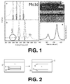
Fig. 1 a is an XPS spectrum of the Mo oxide film formed in step a of an embodiment of the present invention. -
Fig. 1 b is an XPS spectrum of the MoS2 film formed in step b of an embodiment of the present invention. -
Fig. 1 c is a tunnelling electron microscopy (TEM) cross-section of a MoS2 film obtained according to embodiments of the first aspect of the present invention. -
Fig. 1 d is a Raman spectrum of a MoS2 obtained in an embodiment of the first aspect of the present invention. -
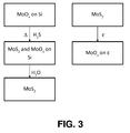
Fig. 2 is a schematic representation of an embodiment of step c of the first aspect of the present invention. -
Fig. 3 is a block diagram illustrating a highly simplified form of the invention - The present invention will be described with respect to particular embodiments and with reference to certain drawings but the invention is not limited thereto but only by the claims. The drawings described are only schematic and are non-limiting. In the drawings, the size of some of the elements may be exaggerated and not drawn on scale for illustrative purposes. The dimensions and the relative dimensions do not correspond to actual reductions to practice of the invention.
- Furthermore, the terms first, second, third and the like in the description and in the claims, are used for distinguishing between similar elements and not necessarily for describing a sequence, either temporally, spatially, in ranking or in any other manner. It is to be understood that the terms so used are interchangeable under appropriate circumstances and that the embodiments of the invention described herein are capable of operation in other sequences than described or illustrated herein.
- Moreover, the terms top, bottom, over, under and the like in the description and the claims are used for descriptive purposes and not necessarily for describing relative positions. It is to be understood that the terms so used are interchangeable under appropriate circumstances and that the embodiments of the invention described herein are capable of operation in other orientations than described or illustrated herein.
- It is to be noticed that the term "comprising", used in the claims, should not be interpreted as being restricted to the means listed thereafter; it does not exclude other elements or steps. It is thus to be interpreted as specifying the presence of the stated features, integers, steps or components as referred to, but does not preclude the presence or addition of one or more other features, integers, steps or components, or groups thereof. Thus, the scope of the expression "a device comprising means A and B" should not be limited to devices consisting only of components A and B. It means that with respect to the present invention, the only relevant components of the device are A and B.
- Reference throughout this specification to "one embodiment" or "an embodiment" means that a particular feature, structure or characteristic described in connection with the embodiment is included in at least one embodiment of the present invention. Thus, appearances of the phrases "in one embodiment" or "in an embodiment" in various places throughout this specification are not necessarily all referring to the same embodiment, but may. Furthermore, the particular features, structures or characteristics may be combined in any suitable manner, as would be apparent to one of ordinary skill in the art from this disclosure, in one or more embodiments.
- Similarly it should be appreciated that in the description of exemplary embodiments of the invention, various features of the invention are sometimes grouped together in a single embodiment, figure, or description thereof for the purpose of streamlining the disclosure and aiding in the understanding of one or more of the various inventive aspects. This method of disclosure, however, is not to be interpreted as reflecting an intention that the claimed invention requires more features than are expressly recited in each claim. Rather, as the following claims reflect, inventive aspects lie in less than all features of a single foregoing disclosed embodiment. Thus, the claims following the detailed description are hereby expressly incorporated into this detailed description, with each claim standing on its own as a separate embodiment of this invention.
- Furthermore, while some embodiments described herein include some but not other features included in other embodiments, combinations of features of different embodiments are meant to be within the scope of the invention, and form different embodiments, as would be understood by those in the art. For example, in the following claims, any of the claimed embodiments can be used in any combination.
- Furthermore, some of the embodiments are described herein as a method or combination of elements of a method that can be implemented by a processor of a computer system or by other means of carrying out the function. Thus, a processor with the necessary instructions for carrying out such a method or element of a method forms a means for carrying out the method or element of a method. Furthermore, an element described herein of an apparatus embodiment is an example of a means for carrying out the function performed by the element for the purpose of carrying out the invention.
- In the description provided herein, numerous specific details are set forth. However, it is understood that embodiments of the invention may be practiced without these specific details. In other instances, well-known methods, structures and techniques have not been shown in detail in order not to obscure an understanding of this description.
- The invention will now be described by a detailed description of several embodiments of the invention. It is clear that other embodiments of the invention can be configured according to the knowledge of persons skilled in the art without departing from the technical teaching of the invention, the invention being limited only by the terms of the appended claims.
- Examples 1, 2, and 3 are illustrated in
Fig. 3 (left). Example 4 is illustrated inFig. 3 (right). - A Si substrate (2x2 cm2) was provided and exposed to a Mo reactive sputtering in O2, thereby acquiring a 5 nm Mo oxide film on its top surface.
- As shown in
Fig. 1 (a) , the film consists of different coexisting Mo oxide phases (MoO3 and Mo2O5). - The sample obtained at the end of example 1 was loaded into a rapid thermal annealing (RTA) system - Annealsys oven AS-ONE150 - for a sulfurization process. To this purpose the sample was annealed in pure H2S (100mbar) at high temperature. Although annealing regime involving temperatures of 400°C or higher typically permitted the obtaining of a MoS2 film, the best results were obtained by a sulfurization process consisting of two annealing steps: 25 minutes at 600°C followed by 5 minutes at 800°C. The first annealing step resulted in the formation of a uniform MoS2 film, while the second step was useful for improving the crystalline quality of the material.
- The tunnelling electron microscopy (TEM) cross-section shown in
Fig. 1 (c) evidences the characteristic layered structure of the MoS2 film. One can observe that the general orientation of the MoS2 sheets is parallel to the substrate. The thickness of the MoS2 film was approximately 8nm (12 molecular planes). - Raman spectroscopy has been used to study the crystalline structure of the synthetic MoS2 film on Si. The Raman spectrum in
Fig. 1 (d) shows two distinctive peaks located at 383cm-1 and 408cm-1: these features corresponds respectively to the in-plane (E2g) mode and the out-of-plane (A1g) mode of MoS2. This observation demonstrates that the sulfurization process resulted in the formation of a uniform MoS2 film with hexagonal crystalline structure and trigonal prismatic coordination geometry. - Additional chemical insights were obtained by x-ray photoemission electron spectroscopy (XPS). The most prominent Mo3d doublet centred at ≈229.5eV (
Fig. 1 (b) ) can be associated with MoS2. A small bump is visible at higher binding energy (236eV). This additional XPS component is related to the presence of residual MoO3. According to Rutherford backscattering spectrometry (RBS) measurements, the oxidized fraction of Mo is expected to be less than 6%. - Without being bound by theory, it is reasonable to assume that the sulfurization process starts from the upper Mo oxide/air interface since it is directly exposed to the H2S gas. For this reason it is reasonable to expect the residual MoO3 to be preferentially located at the interface between the MoS2 film and the underlying Si substrate. MoO3 being known to be slightly soluble in water, it is reasonable to assume that the delamination observed in water (see example 3) between the MoS2 film and the Si substrate is at least partly due to the presence of MoO3 at their interface.
- In order to transfer the MoS2 film onto a dielectric substrate, the synthetic film has to be first detached from the underlying Si substrate while preserving the physical integrity, and the structural and chemical characteristics (uniform thickness, crystalline quality, stoichiometry) of the MoS2 film. We now refer to
Fig. 2 . For this purpose, after the synthesis process described in example 2, the sample (3, 4) was put in a beaker (2) containing deionised water (1). Within a few seconds water penetrated in between the MoS2 film (3) and the underlying substrates (4), starting from the edges. The intercalated water gradually propagated to the centre of the sample (3, 4), thus inducing delamination of the MoS2 film (3). Removing and replacing repeatedly the sample (3, 4) in the beaker helped speeding up delamination. The detached unsupported MoS2 film (3) migrated to the liquid/air interface (5). The supernatant MoS2 film (3) was then ready for the transfer process of example 4. - Dip-coating techniques are conventionally used to transfer graphene or MoS2 films onto dielectric substrates (ε) for optical detection and electrical measurements. Dip coating techniques can be described as processes where the substrate (ε) to be coated is immersed in a liquid and then withdrawn at a constant speed.
- Here, a fresh silicon plate overlaid by a SiO2 layer was used as the substrate (ε). This substrate was used to fish out the supernatant MoS2 film, followed by drying it on a hot-plate (90 °C for 5 min). An optical and scanning electron microscopy (SEM) image (not shown) indicated that the MoS2 film after transfer onto the SiO2/Si substrate (ε) is intact and uniform in thickness. Importantly the normalized Raman spectra before (MoS2/Si) and after transfer
- (MoS2/SiO2) were almost identical (not shown). This observation demonstrates that the crystalline quality and chemical composition of the as-grown MoS2 film were preserved during the transfer process.
- It is to be understood that although preferred embodiments, specific constructions and configurations, as well as materials, have been discussed herein for devices according to the present invention, various changes or modifications in form and detail may be made without departing from the scope of this invention. Functionality may be added or deleted from the block diagrams and operations may be interchanged among functional blocks. Steps may be added or deleted to methods described within the scope of the present invention.
Claims (15)
- A method for forming an unsupported MoS2 layer (3) in an aqueous medium (1), the method comprising the steps of:a. Providing an assembly of a Mo oxide layer on a Si substrate (4);b. Annealing said assembly in presence of H2S at a temperature sufficient for forming a MoS2 layer (3); andc. Contacting the annealed assembly (3, 4) with an aqueous medium (1).
- The method according to claim 1, wherein step c is performed by immersion of the annealed assembly (3, 4) in the aqueous medium (1).
- A method for providing a MoS2 layer (4) on a second substrate (ε) other than the Si substrate (4) of claim 1, the method comprising:i. forming an unsupported MoS2 layer (3) in an aqueous medium (1) by the method of claim 1 or claim 2,ii. dip coating the second substrate (ε) by immersing the second substrate in the aqueous medium (1), then withdrawing the second substrate (ε) from the aqueous medium (1), thereby coating the second substrate (ε) with the unsupported MoS2 layer.
- The method according to claim 3, wherein the second substrate (ε) is a dielectric substrate (ε).
- The method according to any one of claims 1 to 4 wherein the area of the MoS2 layer is at least 1 cm2.
- The method according to any one of the preceding claims, wherein the annealing step b is performed in presence of pure H2S.
- The method according to any one of the preceding claims, wherein the annealing step b is performed at a pressure of from 50 to 200 mbar.
- The method according to any one of the preceding claims, wherein the annealing step b comprises a first annealing step b1 at a temperature of from 520 to 680°C for from 5 to 50 minutes and a second annealing step b2 at a temperature of from 720 to 880°C for from 1 to 10 minutes.
- The method according to any one of the preceding claims, wherein the layer (3) obtained after the annealing step b comprises residual MoO3.
- The method according to claim 9, wherein the residual MoO3 represents from 1 to 12% of the annealed layer (3).
- The method according to claim 9 or claim 10 wherein the residual MoO3 is a layer located at the interface between the Si substrate (4) and the MoS2 layer (3).
- An assembly comprising:a. a Si substrate (4) wherein n is from 0 to 1,b. a MoO3 layer overlaying said substrate, andc. a MoS2 layer overlaying (3) said MoO3 layer.
- An unsupported MoS2 layer obtainable by the method of claim 1.
- An assembly of a MoS2 layer (3) on a dielectric substrate obtainable by the method of claim 4.
- A semiconductor device comprising an assembly according to claim 14.
Priority Applications (2)
| Application Number | Priority Date | Filing Date | Title |
|---|---|---|---|
| EP15150151.7A EP3023390B1 (en) | 2014-11-18 | 2015-01-06 | MoS2 film formation and transfer to a substrate |
| US14/938,657 US9472401B2 (en) | 2014-11-18 | 2015-11-11 | Molybdenum disulfide film formation and transfer to a substrate |
Applications Claiming Priority (2)
| Application Number | Priority Date | Filing Date | Title |
|---|---|---|---|
| EP14193712 | 2014-11-18 | ||
| EP15150151.7A EP3023390B1 (en) | 2014-11-18 | 2015-01-06 | MoS2 film formation and transfer to a substrate |
Publications (2)
| Publication Number | Publication Date |
|---|---|
| EP3023390A1 true EP3023390A1 (en) | 2016-05-25 |
| EP3023390B1 EP3023390B1 (en) | 2019-04-10 |
Family
ID=51982405
Family Applications (1)
| Application Number | Title | Priority Date | Filing Date |
|---|---|---|---|
| EP15150151.7A Active EP3023390B1 (en) | 2014-11-18 | 2015-01-06 | MoS2 film formation and transfer to a substrate |
Country Status (2)
| Country | Link |
|---|---|
| US (1) | US9472401B2 (en) |
| EP (1) | EP3023390B1 (en) |
Cited By (2)
| Publication number | Priority date | Publication date | Assignee | Title |
|---|---|---|---|---|
| CN113649249A (en) * | 2021-09-02 | 2021-11-16 | 西安交通大学 | Nano molybdenum disulfide-based thin film and preparation method thereof |
| CN115802876A (en) * | 2022-10-27 | 2023-03-14 | 集美大学 | Transition metal sulfide thin film and manufacturing method thereof, resistive random access memory and manufacturing method thereof |
Families Citing this family (7)
| Publication number | Priority date | Publication date | Assignee | Title |
|---|---|---|---|---|
| US9991122B2 (en) | 2016-08-31 | 2018-06-05 | Micron Technology, Inc. | Methods of forming semiconductor device structures including two-dimensional material structures |
| CN108588673B (en) * | 2017-07-21 | 2019-11-12 | 杭州电子科技大学 | A kind of preparation method of molybdenum disulfide film |
| CN107464847A (en) * | 2017-07-25 | 2017-12-12 | 西安电子科技大学 | Crystal of molybdenum disulfide pipe and preparation method based on alkali metal soln doping |
| KR102608959B1 (en) | 2017-09-04 | 2023-12-01 | 삼성전자주식회사 | Device comprising 2D material |
| KR102334380B1 (en) | 2017-09-04 | 2021-12-02 | 삼성전자 주식회사 | Method for fabricating device comprising two-dimensional material |
| US10916426B2 (en) * | 2018-05-25 | 2021-02-09 | Applied Materials, Inc. | Formation of crystalline, layered transition metal dichalcogenides |
| CN118479542A (en) * | 2024-05-08 | 2024-08-13 | 云南大学 | Gold-assisted stripping and transferring molybdenum disulfide method |
Citations (2)
| Publication number | Priority date | Publication date | Assignee | Title |
|---|---|---|---|---|
| EP0580019A1 (en) * | 1992-07-08 | 1994-01-26 | Yeda Research And Development Company, Ltd. | Oriented polycrystalline thin films of transition metal chalcogenides |
| US20140245946A1 (en) * | 2013-03-01 | 2014-09-04 | Massachusetts Institute Of Technology | Synthesis and Transfer of Transition Metal Disulfide Layers on Diverse Surfaces |
Family Cites Families (8)
| Publication number | Priority date | Publication date | Assignee | Title |
|---|---|---|---|---|
| US6451729B1 (en) * | 1999-10-06 | 2002-09-17 | The Penn State Research Foundation | Method for preparing a highly active, unsupported high surface-area MoS2 catalyst |
| US8226809B2 (en) * | 2006-01-12 | 2012-07-24 | GM Global Technology Operations LLC | Anodized substrate layer with solid lubricant |
| US7955588B2 (en) * | 2009-05-26 | 2011-06-07 | Conocophillips Company | Metal sulfide catalysts and methods of making same |
| EP2377971A1 (en) * | 2010-04-16 | 2011-10-19 | EPFL Ecole Polytechnique Fédérale de Lausanne | Amorphous transition metal sulphide films or solids as efficient electrocatalysts for hydrogen production from water or aqueous solutions |
| US9000415B2 (en) * | 2012-09-12 | 2015-04-07 | Lg Innotek Co., Ltd. | Light emitting device |
| US9527062B2 (en) * | 2013-05-09 | 2016-12-27 | North Carolina State University | Process for scalable synthesis of molybdenum disulfide monolayer and few-layer films |
| US9896340B2 (en) * | 2013-07-18 | 2018-02-20 | William Marsh Rice University | Rebar hybrid materials and methods of making the same |
| KR102232756B1 (en) * | 2014-05-19 | 2021-03-26 | 삼성전자주식회사 | Electronic device having graphene-semiconductor multi junction and method of manufacturing the same |
-
2015
- 2015-01-06 EP EP15150151.7A patent/EP3023390B1/en active Active
- 2015-11-11 US US14/938,657 patent/US9472401B2/en active Active
Patent Citations (2)
| Publication number | Priority date | Publication date | Assignee | Title |
|---|---|---|---|---|
| EP0580019A1 (en) * | 1992-07-08 | 1994-01-26 | Yeda Research And Development Company, Ltd. | Oriented polycrystalline thin films of transition metal chalcogenides |
| US20140245946A1 (en) * | 2013-03-01 | 2014-09-04 | Massachusetts Institute Of Technology | Synthesis and Transfer of Transition Metal Disulfide Layers on Diverse Surfaces |
Non-Patent Citations (7)
| Title |
|---|
| AREND M. VAN DER ZANDE ET AL., NATURE MATERIALS, vol. 12, 2013, pages 554 - 561 |
| B. RADISAVLJEVIC ET AL., NAT. NANOTECH., vol. 6, 2011, pages 147 |
| KENG-KU LIU ET AL., NANO LETT., vol. 12, no. 3, 2012, pages 1538 |
| MASIHHUR R. LASKAR ET AL., APPL. PHYS. LETT., vol. 102, 2013, pages 252108 |
| SENTHILKUMAR V ET AL: "Direct vapor phase growth process and robust photoluminescence properties of large area MoS2layers", NANO RESEARCH, TSINGHUA UNIVERSITY PRESS, CN, vol. 7, no. 12, 25 August 2014 (2014-08-25), pages 1759 - 1768, XP035464857, ISSN: 1998-0124, [retrieved on 20140825], DOI: 10.1007/S12274-014-0535-7 * |
| XIAO HUANG ET AL: "Metal dichalcogenide nanosheets: preparation, properties and applications", CHEMICAL SOCIETY REVIEWS., vol. 42, no. 5, 7 March 2013 (2013-03-07), GB, pages 1934, XP055221461, ISSN: 0306-0012, DOI: 10.1039/c2cs35387c * |
| YU-CHUAN LIN ET AL: "Wafer-scale MoS2 thin layers prepared by MoO3 sulfurization", NANOSCALE, vol. 4, no. 20, 29 August 2012 (2012-08-29), United Kingdom, pages 6637, XP055221104, ISSN: 2040-3364, DOI: 10.1039/c2nr31833d * |
Cited By (2)
| Publication number | Priority date | Publication date | Assignee | Title |
|---|---|---|---|---|
| CN113649249A (en) * | 2021-09-02 | 2021-11-16 | 西安交通大学 | Nano molybdenum disulfide-based thin film and preparation method thereof |
| CN115802876A (en) * | 2022-10-27 | 2023-03-14 | 集美大学 | Transition metal sulfide thin film and manufacturing method thereof, resistive random access memory and manufacturing method thereof |
Also Published As
| Publication number | Publication date |
|---|---|
| US9472401B2 (en) | 2016-10-18 |
| US20160141174A1 (en) | 2016-05-19 |
| EP3023390B1 (en) | 2019-04-10 |
Similar Documents
| Publication | Publication Date | Title |
|---|---|---|
| EP3023390B1 (en) | MoS2 film formation and transfer to a substrate | |
| CN107170711B (en) | Method for preparing two-dimensional atomic crystal laminated structure by transfer | |
| Liu et al. | Graphene-assisted metal transfer printing for wafer-scale integration of metal electrodes and two-dimensional materials | |
| Satterthwaite et al. | Van der Waals device integration beyond the limits of van der Waals forces using adhesive matrix transfer | |
| Fan et al. | Transfer assembly for two-dimensional van der Waals heterostructures | |
| Kinoshita et al. | Dry release transfer of graphene and few-layer h-BN by utilizing thermoplasticity of polypropylene carbonate | |
| Lu et al. | Synthesis of freestanding single-crystal perovskite films and heterostructures by etching of sacrificial water-soluble layers | |
| Shinde et al. | Surface‐functionalization‐mediated direct transfer of molybdenum disulfide for large‐area flexible devices | |
| Toko et al. | Highly (111)-oriented Ge thin films on insulators formed by Al-induced crystallization | |
| Ma et al. | Van der Waals epitaxy of functional MoO2 film on mica for flexible electronics | |
| Ryu et al. | Amorphous-InGaZnO4 thin-film transistors with damage-free back channel wet-etch process | |
| Zheng et al. | Electrostatic-repulsion-based transfer of van der Waals materials | |
| US9087692B2 (en) | Method for transferring a graphene layer | |
| Qi et al. | Wax-assisted crack-free transfer of monolayer CVD graphene: Extending from standalone to supported copper substrates | |
| US10369775B2 (en) | Method of releasing graphene from substrate | |
| Xu et al. | Facile passivation of solution-processed InZnO thin-film transistors by octadecylphosphonic acid self-assembled monolayers at room temperature | |
| Wan et al. | Interface engineering for CVD graphene: current status and progress | |
| Cai et al. | The development of transfer technologies for advanced 2D circuits integration | |
| Koren et al. | Isolation of high quality graphene from Ru by solution phase intercalation | |
| Zhang et al. | Se-mediated dry transfer of wafer-scale 2D semiconductors for advanced electronics | |
| Graham et al. | NaCl substrates for high temperature processing and transfer of ultrathin materials | |
| Budania et al. | Effect of post-exfoliation treatments on mechanically exfoliated MoS2 | |
| Fan et al. | Strategy for transferring van der Waals materials and heterostructures | |
| Bedell et al. | Advanced flexible electronics: challenges and opportunities | |
| CN104528664B (en) | The preparation method of two dimension telluride gallium material |
Legal Events
| Date | Code | Title | Description |
|---|---|---|---|
| AK | Designated contracting states |
Kind code of ref document: A1 Designated state(s): AL AT BE BG CH CY CZ DE DK EE ES FI FR GB GR HR HU IE IS IT LI LT LU LV MC MK MT NL NO PL PT RO RS SE SI SK SM TR |
|
| AX | Request for extension of the european patent |
Extension state: BA ME |
|
| PUAI | Public reference made under article 153(3) epc to a published international application that has entered the european phase |
Free format text: ORIGINAL CODE: 0009012 |
|
| STAA | Information on the status of an ep patent application or granted ep patent |
Free format text: STATUS: REQUEST FOR EXAMINATION WAS MADE |
|
| 17P | Request for examination filed |
Effective date: 20161121 |
|
| RBV | Designated contracting states (corrected) |
Designated state(s): AL AT BE BG CH CY CZ DE DK EE ES FI FR GB GR HR HU IE IS IT LI LT LU LV MC MK MT NL NO PL PT RO RS SE SI SK SM TR |
|
| STAA | Information on the status of an ep patent application or granted ep patent |
Free format text: STATUS: EXAMINATION IS IN PROGRESS |
|
| 17Q | First examination report despatched |
Effective date: 20180524 |
|
| GRAP | Despatch of communication of intention to grant a patent |
Free format text: ORIGINAL CODE: EPIDOSNIGR1 |
|
| STAA | Information on the status of an ep patent application or granted ep patent |
Free format text: STATUS: GRANT OF PATENT IS INTENDED |
|
| RIC1 | Information provided on ipc code assigned before grant |
Ipc: H01L 21/02 20060101ALI20180928BHEP Ipc: C01G 39/02 20060101AFI20180928BHEP Ipc: C01G 39/06 20060101ALI20180928BHEP Ipc: H01L 21/324 20060101ALI20180928BHEP |
|
| INTG | Intention to grant announced |
Effective date: 20181025 |
|
| GRAS | Grant fee paid |
Free format text: ORIGINAL CODE: EPIDOSNIGR3 |
|
| GRAA | (expected) grant |
Free format text: ORIGINAL CODE: 0009210 |
|
| STAA | Information on the status of an ep patent application or granted ep patent |
Free format text: STATUS: THE PATENT HAS BEEN GRANTED |
|
| AK | Designated contracting states |
Kind code of ref document: B1 Designated state(s): AL AT BE BG CH CY CZ DE DK EE ES FI FR GB GR HR HU IE IS IT LI LT LU LV MC MK MT NL NO PL PT RO RS SE SI SK SM TR |
|
| REG | Reference to a national code |
Ref country code: GB Ref legal event code: FG4D |
|
| REG | Reference to a national code |
Ref country code: CH Ref legal event code: EP Ref country code: AT Ref legal event code: REF Ref document number: 1118406 Country of ref document: AT Kind code of ref document: T Effective date: 20190415 |
|
| REG | Reference to a national code |
Ref country code: IE Ref legal event code: FG4D |
|
| REG | Reference to a national code |
Ref country code: DE Ref legal event code: R096 Ref document number: 602015027853 Country of ref document: DE |
|
| REG | Reference to a national code |
Ref country code: NL Ref legal event code: MP Effective date: 20190410 |
|
| REG | Reference to a national code |
Ref country code: LT Ref legal event code: MG4D |
|
| REG | Reference to a national code |
Ref country code: AT Ref legal event code: MK05 Ref document number: 1118406 Country of ref document: AT Kind code of ref document: T Effective date: 20190410 |
|
| PG25 | Lapsed in a contracting state [announced via postgrant information from national office to epo] |
Ref country code: NL Free format text: LAPSE BECAUSE OF FAILURE TO SUBMIT A TRANSLATION OF THE DESCRIPTION OR TO PAY THE FEE WITHIN THE PRESCRIBED TIME-LIMIT Effective date: 20190410 |
|
| PG25 | Lapsed in a contracting state [announced via postgrant information from national office to epo] |
Ref country code: NO Free format text: LAPSE BECAUSE OF FAILURE TO SUBMIT A TRANSLATION OF THE DESCRIPTION OR TO PAY THE FEE WITHIN THE PRESCRIBED TIME-LIMIT Effective date: 20190710 Ref country code: FI Free format text: LAPSE BECAUSE OF FAILURE TO SUBMIT A TRANSLATION OF THE DESCRIPTION OR TO PAY THE FEE WITHIN THE PRESCRIBED TIME-LIMIT Effective date: 20190410 Ref country code: PT Free format text: LAPSE BECAUSE OF FAILURE TO SUBMIT A TRANSLATION OF THE DESCRIPTION OR TO PAY THE FEE WITHIN THE PRESCRIBED TIME-LIMIT Effective date: 20190910 Ref country code: SE Free format text: LAPSE BECAUSE OF FAILURE TO SUBMIT A TRANSLATION OF THE DESCRIPTION OR TO PAY THE FEE WITHIN THE PRESCRIBED TIME-LIMIT Effective date: 20190410 Ref country code: AL Free format text: LAPSE BECAUSE OF FAILURE TO SUBMIT A TRANSLATION OF THE DESCRIPTION OR TO PAY THE FEE WITHIN THE PRESCRIBED TIME-LIMIT Effective date: 20190410 Ref country code: HR Free format text: LAPSE BECAUSE OF FAILURE TO SUBMIT A TRANSLATION OF THE DESCRIPTION OR TO PAY THE FEE WITHIN THE PRESCRIBED TIME-LIMIT Effective date: 20190410 Ref country code: LT Free format text: LAPSE BECAUSE OF FAILURE TO SUBMIT A TRANSLATION OF THE DESCRIPTION OR TO PAY THE FEE WITHIN THE PRESCRIBED TIME-LIMIT Effective date: 20190410 Ref country code: ES Free format text: LAPSE BECAUSE OF FAILURE TO SUBMIT A TRANSLATION OF THE DESCRIPTION OR TO PAY THE FEE WITHIN THE PRESCRIBED TIME-LIMIT Effective date: 20190410 |
|
| PG25 | Lapsed in a contracting state [announced via postgrant information from national office to epo] |
Ref country code: LV Free format text: LAPSE BECAUSE OF FAILURE TO SUBMIT A TRANSLATION OF THE DESCRIPTION OR TO PAY THE FEE WITHIN THE PRESCRIBED TIME-LIMIT Effective date: 20190410 Ref country code: RS Free format text: LAPSE BECAUSE OF FAILURE TO SUBMIT A TRANSLATION OF THE DESCRIPTION OR TO PAY THE FEE WITHIN THE PRESCRIBED TIME-LIMIT Effective date: 20190410 Ref country code: GR Free format text: LAPSE BECAUSE OF FAILURE TO SUBMIT A TRANSLATION OF THE DESCRIPTION OR TO PAY THE FEE WITHIN THE PRESCRIBED TIME-LIMIT Effective date: 20190711 Ref country code: BG Free format text: LAPSE BECAUSE OF FAILURE TO SUBMIT A TRANSLATION OF THE DESCRIPTION OR TO PAY THE FEE WITHIN THE PRESCRIBED TIME-LIMIT Effective date: 20190710 Ref country code: PL Free format text: LAPSE BECAUSE OF FAILURE TO SUBMIT A TRANSLATION OF THE DESCRIPTION OR TO PAY THE FEE WITHIN THE PRESCRIBED TIME-LIMIT Effective date: 20190410 |
|
| PG25 | Lapsed in a contracting state [announced via postgrant information from national office to epo] |
Ref country code: IS Free format text: LAPSE BECAUSE OF FAILURE TO SUBMIT A TRANSLATION OF THE DESCRIPTION OR TO PAY THE FEE WITHIN THE PRESCRIBED TIME-LIMIT Effective date: 20190810 Ref country code: AT Free format text: LAPSE BECAUSE OF FAILURE TO SUBMIT A TRANSLATION OF THE DESCRIPTION OR TO PAY THE FEE WITHIN THE PRESCRIBED TIME-LIMIT Effective date: 20190410 |
|
| REG | Reference to a national code |
Ref country code: DE Ref legal event code: R097 Ref document number: 602015027853 Country of ref document: DE |
|
| PG25 | Lapsed in a contracting state [announced via postgrant information from national office to epo] |
Ref country code: CZ Free format text: LAPSE BECAUSE OF FAILURE TO SUBMIT A TRANSLATION OF THE DESCRIPTION OR TO PAY THE FEE WITHIN THE PRESCRIBED TIME-LIMIT Effective date: 20190410 Ref country code: RO Free format text: LAPSE BECAUSE OF FAILURE TO SUBMIT A TRANSLATION OF THE DESCRIPTION OR TO PAY THE FEE WITHIN THE PRESCRIBED TIME-LIMIT Effective date: 20190410 Ref country code: SK Free format text: LAPSE BECAUSE OF FAILURE TO SUBMIT A TRANSLATION OF THE DESCRIPTION OR TO PAY THE FEE WITHIN THE PRESCRIBED TIME-LIMIT Effective date: 20190410 Ref country code: DK Free format text: LAPSE BECAUSE OF FAILURE TO SUBMIT A TRANSLATION OF THE DESCRIPTION OR TO PAY THE FEE WITHIN THE PRESCRIBED TIME-LIMIT Effective date: 20190410 Ref country code: EE Free format text: LAPSE BECAUSE OF FAILURE TO SUBMIT A TRANSLATION OF THE DESCRIPTION OR TO PAY THE FEE WITHIN THE PRESCRIBED TIME-LIMIT Effective date: 20190410 |
|
| PLBE | No opposition filed within time limit |
Free format text: ORIGINAL CODE: 0009261 |
|
| STAA | Information on the status of an ep patent application or granted ep patent |
Free format text: STATUS: NO OPPOSITION FILED WITHIN TIME LIMIT |
|
| PG25 | Lapsed in a contracting state [announced via postgrant information from national office to epo] |
Ref country code: IT Free format text: LAPSE BECAUSE OF FAILURE TO SUBMIT A TRANSLATION OF THE DESCRIPTION OR TO PAY THE FEE WITHIN THE PRESCRIBED TIME-LIMIT Effective date: 20190410 Ref country code: SM Free format text: LAPSE BECAUSE OF FAILURE TO SUBMIT A TRANSLATION OF THE DESCRIPTION OR TO PAY THE FEE WITHIN THE PRESCRIBED TIME-LIMIT Effective date: 20190410 |
|
| 26N | No opposition filed |
Effective date: 20200113 |
|
| PG25 | Lapsed in a contracting state [announced via postgrant information from national office to epo] |
Ref country code: TR Free format text: LAPSE BECAUSE OF FAILURE TO SUBMIT A TRANSLATION OF THE DESCRIPTION OR TO PAY THE FEE WITHIN THE PRESCRIBED TIME-LIMIT Effective date: 20190410 |
|
| PG25 | Lapsed in a contracting state [announced via postgrant information from national office to epo] |
Ref country code: SI Free format text: LAPSE BECAUSE OF FAILURE TO SUBMIT A TRANSLATION OF THE DESCRIPTION OR TO PAY THE FEE WITHIN THE PRESCRIBED TIME-LIMIT Effective date: 20190410 |
|
| PG25 | Lapsed in a contracting state [announced via postgrant information from national office to epo] |
Ref country code: MC Free format text: LAPSE BECAUSE OF FAILURE TO SUBMIT A TRANSLATION OF THE DESCRIPTION OR TO PAY THE FEE WITHIN THE PRESCRIBED TIME-LIMIT Effective date: 20190410 |
|
| REG | Reference to a national code |
Ref country code: CH Ref legal event code: PL |
|
| GBPC | Gb: european patent ceased through non-payment of renewal fee |
Effective date: 20200106 |
|
| REG | Reference to a national code |
Ref country code: BE Ref legal event code: MM Effective date: 20200131 |
|
| PG25 | Lapsed in a contracting state [announced via postgrant information from national office to epo] |
Ref country code: GB Free format text: LAPSE BECAUSE OF NON-PAYMENT OF DUE FEES Effective date: 20200106 Ref country code: LU Free format text: LAPSE BECAUSE OF NON-PAYMENT OF DUE FEES Effective date: 20200106 |
|
| PG25 | Lapsed in a contracting state [announced via postgrant information from national office to epo] |
Ref country code: CH Free format text: LAPSE BECAUSE OF NON-PAYMENT OF DUE FEES Effective date: 20200131 Ref country code: LI Free format text: LAPSE BECAUSE OF NON-PAYMENT OF DUE FEES Effective date: 20200131 Ref country code: BE Free format text: LAPSE BECAUSE OF NON-PAYMENT OF DUE FEES Effective date: 20200131 |
|
| PG25 | Lapsed in a contracting state [announced via postgrant information from national office to epo] |
Ref country code: IE Free format text: LAPSE BECAUSE OF NON-PAYMENT OF DUE FEES Effective date: 20200106 |
|
| PG25 | Lapsed in a contracting state [announced via postgrant information from national office to epo] |
Ref country code: MT Free format text: LAPSE BECAUSE OF FAILURE TO SUBMIT A TRANSLATION OF THE DESCRIPTION OR TO PAY THE FEE WITHIN THE PRESCRIBED TIME-LIMIT Effective date: 20190410 Ref country code: CY Free format text: LAPSE BECAUSE OF FAILURE TO SUBMIT A TRANSLATION OF THE DESCRIPTION OR TO PAY THE FEE WITHIN THE PRESCRIBED TIME-LIMIT Effective date: 20190410 |
|
| PG25 | Lapsed in a contracting state [announced via postgrant information from national office to epo] |
Ref country code: MK Free format text: LAPSE BECAUSE OF FAILURE TO SUBMIT A TRANSLATION OF THE DESCRIPTION OR TO PAY THE FEE WITHIN THE PRESCRIBED TIME-LIMIT Effective date: 20190410 |
|
| P01 | Opt-out of the competence of the unified patent court (upc) registered |
Effective date: 20230513 |
|
| PGFP | Annual fee paid to national office [announced via postgrant information from national office to epo] |
Ref country code: FR Payment date: 20251217 Year of fee payment: 12 |
|
| PGFP | Annual fee paid to national office [announced via postgrant information from national office to epo] |
Ref country code: DE Payment date: 20251217 Year of fee payment: 12 |