EP3021483A1 - Amplifier and related method - Google Patents
Amplifier and related method Download PDFInfo
- Publication number
- EP3021483A1 EP3021483A1 EP15192244.0A EP15192244A EP3021483A1 EP 3021483 A1 EP3021483 A1 EP 3021483A1 EP 15192244 A EP15192244 A EP 15192244A EP 3021483 A1 EP3021483 A1 EP 3021483A1
- Authority
- EP
- European Patent Office
- Prior art keywords
- pcc
- scc
- circuit
- slice
- amplifier circuit
- Prior art date
- Legal status (The legal status is an assumption and is not a legal conclusion. Google has not performed a legal analysis and makes no representation as to the accuracy of the status listed.)
- Granted
Links
Images





Classifications
-
- H—ELECTRICITY
- H03—ELECTRONIC CIRCUITRY
- H03F—AMPLIFIERS
- H03F3/00—Amplifiers with only discharge tubes or only semiconductor devices as amplifying elements
- H03F3/189—High-frequency amplifiers, e.g. radio frequency amplifiers
- H03F3/19—High-frequency amplifiers, e.g. radio frequency amplifiers with semiconductor devices only
- H03F3/193—High-frequency amplifiers, e.g. radio frequency amplifiers with semiconductor devices only with field-effect devices
-
- H—ELECTRICITY
- H03—ELECTRONIC CIRCUITRY
- H03F—AMPLIFIERS
- H03F1/00—Details of amplifiers with only discharge tubes, only semiconductor devices or only unspecified devices as amplifying elements
- H03F1/02—Modifications of amplifiers to raise the efficiency, e.g. gliding Class A stages, use of an auxiliary oscillation
- H03F1/0205—Modifications of amplifiers to raise the efficiency, e.g. gliding Class A stages, use of an auxiliary oscillation in transistor amplifiers
- H03F1/0277—Selecting one or more amplifiers from a plurality of amplifiers
-
- H—ELECTRICITY
- H03—ELECTRONIC CIRCUITRY
- H03F—AMPLIFIERS
- H03F1/00—Details of amplifiers with only discharge tubes, only semiconductor devices or only unspecified devices as amplifying elements
- H03F1/08—Modifications of amplifiers to reduce detrimental influences of internal impedances of amplifying elements
- H03F1/22—Modifications of amplifiers to reduce detrimental influences of internal impedances of amplifying elements by use of cascode coupling, i.e. earthed cathode or emitter stage followed by earthed grid or base stage respectively
- H03F1/223—Modifications of amplifiers to reduce detrimental influences of internal impedances of amplifying elements by use of cascode coupling, i.e. earthed cathode or emitter stage followed by earthed grid or base stage respectively with MOSFET's
-
- H—ELECTRICITY
- H03—ELECTRONIC CIRCUITRY
- H03F—AMPLIFIERS
- H03F3/00—Amplifiers with only discharge tubes or only semiconductor devices as amplifying elements
- H03F3/20—Power amplifiers, e.g. Class B amplifiers, Class C amplifiers
- H03F3/21—Power amplifiers, e.g. Class B amplifiers, Class C amplifiers with semiconductor devices only
- H03F3/211—Power amplifiers, e.g. Class B amplifiers, Class C amplifiers with semiconductor devices only using a combination of several amplifiers
-
- H—ELECTRICITY
- H03—ELECTRONIC CIRCUITRY
- H03F—AMPLIFIERS
- H03F3/00—Amplifiers with only discharge tubes or only semiconductor devices as amplifying elements
- H03F3/68—Combinations of amplifiers, e.g. multi-channel amplifiers for stereophonics
-
- H—ELECTRICITY
- H03—ELECTRONIC CIRCUITRY
- H03F—AMPLIFIERS
- H03F3/00—Amplifiers with only discharge tubes or only semiconductor devices as amplifying elements
- H03F3/72—Gated amplifiers, i.e. amplifiers which are rendered operative or inoperative by means of a control signal
-
- H—ELECTRICITY
- H04—ELECTRIC COMMUNICATION TECHNIQUE
- H04B—TRANSMISSION
- H04B1/00—Details of transmission systems, not covered by a single one of groups H04B3/00 - H04B13/00; Details of transmission systems not characterised by the medium used for transmission
- H04B1/02—Transmitters
- H04B1/04—Circuits
-
- H—ELECTRICITY
- H03—ELECTRONIC CIRCUITRY
- H03F—AMPLIFIERS
- H03F2200/00—Indexing scheme relating to amplifiers
- H03F2200/111—Indexing scheme relating to amplifiers the amplifier being a dual or triple band amplifier, e.g. 900 and 1800 MHz, e.g. switched or not switched, simultaneously or not
-
- H—ELECTRICITY
- H03—ELECTRONIC CIRCUITRY
- H03F—AMPLIFIERS
- H03F2200/00—Indexing scheme relating to amplifiers
- H03F2200/129—Indexing scheme relating to amplifiers there being a feedback over the complete amplifier
-
- H—ELECTRICITY
- H03—ELECTRONIC CIRCUITRY
- H03F—AMPLIFIERS
- H03F2200/00—Indexing scheme relating to amplifiers
- H03F2200/144—Indexing scheme relating to amplifiers the feedback circuit of the amplifier stage comprising a passive resistor and passive capacitor
-
- H—ELECTRICITY
- H03—ELECTRONIC CIRCUITRY
- H03F—AMPLIFIERS
- H03F2200/00—Indexing scheme relating to amplifiers
- H03F2200/294—Indexing scheme relating to amplifiers the amplifier being a low noise amplifier [LNA]
-
- H—ELECTRICITY
- H03—ELECTRONIC CIRCUITRY
- H03F—AMPLIFIERS
- H03F2200/00—Indexing scheme relating to amplifiers
- H03F2200/451—Indexing scheme relating to amplifiers the amplifier being a radio frequency amplifier
-
- H—ELECTRICITY
- H03—ELECTRONIC CIRCUITRY
- H03F—AMPLIFIERS
- H03F2200/00—Indexing scheme relating to amplifiers
- H03F2200/54—Two or more capacitor coupled amplifier stages in cascade
-
- H—ELECTRICITY
- H03—ELECTRONIC CIRCUITRY
- H03F—AMPLIFIERS
- H03F2200/00—Indexing scheme relating to amplifiers
- H03F2200/75—Indexing scheme relating to amplifiers the amplifier stage being a common source configuration MOSFET
-
- H—ELECTRICITY
- H03—ELECTRONIC CIRCUITRY
- H03F—AMPLIFIERS
- H03F2200/00—Indexing scheme relating to amplifiers
- H03F2200/87—Indexing scheme relating to amplifiers the cross coupling circuit being realised only by MOSFETs
-
- H—ELECTRICITY
- H03—ELECTRONIC CIRCUITRY
- H03F—AMPLIFIERS
- H03F2203/00—Indexing scheme relating to amplifiers with only discharge tubes or only semiconductor devices as amplifying elements covered by H03F3/00
- H03F2203/20—Indexing scheme relating to power amplifiers, e.g. Class B amplifiers, Class C amplifiers
- H03F2203/21—Indexing scheme relating to power amplifiers, e.g. Class B amplifiers, Class C amplifiers with semiconductor devices only
- H03F2203/211—Indexing scheme relating to power amplifiers, e.g. Class B amplifiers, Class C amplifiers with semiconductor devices only using a combination of several amplifiers
- H03F2203/21142—Output signals of a plurality of power amplifiers are parallel combined to a common output
-
- H—ELECTRICITY
- H03—ELECTRONIC CIRCUITRY
- H03F—AMPLIFIERS
- H03F2203/00—Indexing scheme relating to amplifiers with only discharge tubes or only semiconductor devices as amplifying elements covered by H03F3/00
- H03F2203/20—Indexing scheme relating to power amplifiers, e.g. Class B amplifiers, Class C amplifiers
- H03F2203/21—Indexing scheme relating to power amplifiers, e.g. Class B amplifiers, Class C amplifiers with semiconductor devices only
- H03F2203/211—Indexing scheme relating to power amplifiers, e.g. Class B amplifiers, Class C amplifiers with semiconductor devices only using a combination of several amplifiers
- H03F2203/21154—An output signal of a power amplifier being controlled by controlling voltage signal
-
- H—ELECTRICITY
- H03—ELECTRONIC CIRCUITRY
- H03F—AMPLIFIERS
- H03F2203/00—Indexing scheme relating to amplifiers with only discharge tubes or only semiconductor devices as amplifying elements covered by H03F3/00
- H03F2203/20—Indexing scheme relating to power amplifiers, e.g. Class B amplifiers, Class C amplifiers
- H03F2203/21—Indexing scheme relating to power amplifiers, e.g. Class B amplifiers, Class C amplifiers with semiconductor devices only
- H03F2203/211—Indexing scheme relating to power amplifiers, e.g. Class B amplifiers, Class C amplifiers with semiconductor devices only using a combination of several amplifiers
- H03F2203/21175—An output signal of a power amplifier being on/off switched
-
- H—ELECTRICITY
- H03—ELECTRONIC CIRCUITRY
- H03F—AMPLIFIERS
- H03F2203/00—Indexing scheme relating to amplifiers with only discharge tubes or only semiconductor devices as amplifying elements covered by H03F3/00
- H03F2203/72—Indexing scheme relating to gated amplifiers, i.e. amplifiers which are rendered operative or inoperative by means of a control signal
- H03F2203/7206—Indexing scheme relating to gated amplifiers, i.e. amplifiers which are rendered operative or inoperative by means of a control signal the gated amplifier being switched on or off by a switch in the bias circuit of the amplifier controlling a bias voltage in the amplifier
-
- H—ELECTRICITY
- H03—ELECTRONIC CIRCUITRY
- H03F—AMPLIFIERS
- H03F2203/00—Indexing scheme relating to amplifiers with only discharge tubes or only semiconductor devices as amplifying elements covered by H03F3/00
- H03F2203/72—Indexing scheme relating to gated amplifiers, i.e. amplifiers which are rendered operative or inoperative by means of a control signal
- H03F2203/7236—Indexing scheme relating to gated amplifiers, i.e. amplifiers which are rendered operative or inoperative by means of a control signal the gated amplifier being switched on or off by putting into parallel or not, by choosing between amplifiers by (a ) switch(es)
-
- H—ELECTRICITY
- H04—ELECTRIC COMMUNICATION TECHNIQUE
- H04B—TRANSMISSION
- H04B1/00—Details of transmission systems, not covered by a single one of groups H04B3/00 - H04B13/00; Details of transmission systems not characterised by the medium used for transmission
- H04B1/02—Transmitters
- H04B1/04—Circuits
- H04B2001/0408—Circuits with power amplifiers
- H04B2001/0416—Circuits with power amplifiers having gain or transmission power control
Definitions
- the present invention relates to an amplifier, and more particularly, to a low-noise amplifier (LNA) for processing two non-contiguous channels in the same band and a related method according to the pre-characterizing clauses of claims 1 and 9.
- LNA low-noise amplifier
- CAs Carrier aggregations
- LTE Long Term Evolution
- NCA intra-band non-contiguous CA
- the wanted signal level of the two channels may not be equal.
- a multi-output LNA capable of receiving one RF input and generating two RF outputs to different mixers for down-conversion of two channels and further support a function of using different gains for generating output signals to different mixers for down conversion is required.
- one objective of the present invention is to provide an amplifier and a related method for processing two non-contiguous channels in the same band, such as one PCC channel and one SCC channel transmitted using an intra-band non-contiguous carrier aggregation scheme.
- an exemplary amplifier applicable to an intra-band non-contiguous carrier aggregation (NCCA) band includes at least a primary component carrier (PCC) channel and a secondary component carrier (SCC) channel not adjacent to each other.
- the exemplary amplifier includes a first amplifier circuit and a second amplifier circuit.
- the first amplifier circuit is arranged to receive a first input signal and generate a first output signal for undergoing down-conversion of one of the PCC channel and the SCC channel.
- the second amplifier circuit is arranged to receive at least one second input signal and generate a second output signal for undergoing down-conversion of another of the PCC channel and the SCC channel.
- the at least one second input signal received by the second amplifier circuit is provided by the first amplifier circuit according to the first input signal.
- an exemplary method for operating an amplifier applicable to an intra-band non-contiguous carrier aggregation (NCCA) band includes at least a primary component carrier (PCC) channel and a secondary component carrier (SCC) channel not adjacent to each other.
- the exemplary method includes: utilizing a first amplifier circuit to receive a first input signal and generate a first output signal for undergoing down-conversion of one of the PCC channel and the SCC channel; providing at least one second input signal to a second amplifier circuit; and utilizing the second amplifier circuit to receive the at least one second input signal and to generate a second output signal for undergoing down-conversion of another of the PCC channel and the SCC channel.
- the at least one second input signal received by the second amplifier circuit is provided by the first amplifier circuit according to the first input signal.
- FIGs. 1-3 illustrate different carrier aggregation schemes, respectively.
- the intra-band continuous/non-contiguous carrier aggregation occurs when multiple component carriers locate in a same radio frequency (RF) band, as shown in FIGs. 1 and 2 .
- the inter-band carrier aggregation occurs when multiple available component carriers locate in different RF bands, as shown in FIG. 3 .
- RF radio frequency
- the signal channels 102a, 102b locate in Band A and are adjacent to each other.
- the higher-frequency component carrier 102b may be viewed as a primary component carrier (PCC), and the lower-frequency component carrier 102a may be viewed as the secondary component carrier (SCC).
- PCC primary component carrier
- SCC secondary component carrier
- FIG. 2 illustrates an example of intra-band non-contiguous carrier aggregation 200, wherein the component carriers 202a, 202b are both in Band A but are not adjacent to each other.
- the higher-frequency component carrier 202b may be viewed as the PCC, and the lower-frequency component carrier 202a may be viewed as the SCC.
- FIG. 3 illustrates an example of inter-band non-contiguous carrier aggregation 300, wherein the component carriers 302a and 302b are in Band A and Band B, respectively.
- the component carrier 302a may be the PCC and the component carrier 302b may be the SCC.
- the two signal channels are in different reception bands.
- FIG. 2 there is only one receiving band (Band A) and two non-contiguous channels.
- LNA low-noise amplifier
- FIG. 4 is a diagram illustrating an amplifier 400 according to an embodiment of the present invention.
- the amplifier 400 is applied to an NCCA band (e.g. the NCCA band shown in FIG. 2 ).
- the amplifier 400 is a low noise amplifier (LNA) with multiple outputs.
- the amplifier 400 includes a first amplifier circuit (e.g., first LNA circuit) 401 and a second amplifier circuit (e.g., second LNA circuit) 402.
- the first amplifier circuit 401 includes a plurality of first slice circuits (e.g., PCC slice circuits PCC_1-PCC_N), and the second amplifier circuit 402 includes a plurality of second slice circuits (e.g., SCC slice circuits SCC_1-SCC_N), where the plurality of PCC slice circuits PCC_1-PCC_N correspond to the plurality of SCC slice circuits SCC_1-SCC_N, respectively.
- the PCC slice circuits PCC_1-PCC_N are coupled to the SCC slice circuits SCC_1-SCC_N, respectively.
- an input signal of an SCC slice circuit is provided by a corresponding PCC slice circuit.
- the first amplifier circuit 401 is arranged to receive a first input signal S1 and generate a first output signal OUT1 for undergoing down-conversion of the PCC channel at one mixer (not shown), and the second amplifier circuit 402 is arranged to receive at least one second input signal S2 and generate a second output signal OUT2 for undergoing down-conversion of the SCC channel at another mixer (not shown), where the at least one second input signal S2 received by the second amplifier circuit 402 is provided by the first amplifier circuit 401 according to the first input signal S1.
- the first input signal S1 is received from an NCCA band.
- each of the first output signal OUT1 and the second output signal OUT2 is derived from amplifying an input signal directly/indirectly set by the first input signal S1
- each of the first output signal OUT1 and the second output signal OUT2 include PCC channel components and SCC channel components.
- the PCC slice circuit When a PCC slice circuit is turned on, the PCC slice circuit receives the first input signal S1, and amplifies the first input signal S1 to generate an amplified output to an output port N1 of the first amplifier circuit 401. Hence, amplified outputs generated from turned-on PCC slice circuits are combined at the output port N1 of the first amplifier circuit 401 to form the first output signal OUT1 having PCC channel components and SCC channel components. Moreover, the first amplifier circuit 401 is arranged to generate the first output signal OUT1 according to a first gain (e.g., PCC gain), where the first gain is adjusted according to the number of turned-on PCC slice circuits of the first amplifier circuit 401.
- a first gain e.g., PCC gain
- the first output signal OUT1 will undergo down-conversion of the PCC channel.
- the first amplifier circuit 401 with the first gain properly adjusted can ensure that PCC channel components in the first output signal OUT1 have proper magnitude, such that a down-conversion result of the PCC channel will have desired signal magnitude.
- the SCC slice circuit receives a second input signal S2 from a corresponding PCC slice circuit, and amplifies the received second input signal S2 to generate an amplified output to an output port N2 of the second amplifier circuit 402.
- amplified outputs generated from turned-on SCC slice circuits are combined at the output port N2 of the second amplifier circuit 402 to form the second output signal OUT2 having PCC channel components and SCC channel components.
- the second amplifier circuit 402 is arranged to generate the second output signal OUT2 according to a second gain (e.g., SCC gain), where the second gain is adjusted according to the number of turned-on SCC slice circuits of the second amplifier circuit 402.
- the second output signal OUT2 will undergo down-conversion of the SCC channel.
- the second amplifier circuit 402 with the second gain properly adjusted can ensure that SCC channel components in the second output signal OUT1 have proper magnitude, such that a down-conversion result of the SCC channel will have desired signal magnitude.
- the PCC slice circuits PCC_1-PCC_N may include low-gain slice circuits and high-gain slice circuits
- the SCC slice circuits SCC_1-SCC_N may include low-gain slice circuits and high-gain slice circuits.
- the PCC slice circuit PCC_N and the SCC slice circuit SCC_N shown in FIG. 4 may be low-gain slice circuits
- the PCC slice circuits PCC_1-PCC_2 and the SCC slice circuits SCC_1-SCC_2 shown in FIG. 4 may be high-gain slice circuits.
- the high-gain slice circuit and the low-gain slice circuit have different amplifier structures with different gain settings.
- the high-gain slice circuit may employ a shunt-shunt feedback LNA structure.
- all of the PCC slice circuits PCC_1-PCC_N may be high-gain slice circuits
- all of the SCC slice circuits SCC_1-SCC_N may be high-gain slice circuits.
- FIG. 5 is a diagram illustrating a partial circuit structure 400_1 of the amplifier 400 shown in FIG. 4 according to an embodiment of the present invention. For example, only four slice circuits are shown in FIG. 5 for illustrative purposes.
- the partial circuit structure 400_1 includes two PCC slice circuits 411 and 413 and two SCC slice circuits 412 and 414.
- the PCC slice circuit 411 and the SCC slice circuit 412 may be high-gain slice circuits for a high-gain path/high-gain mode
- the PCC slice circuit 413 and the SCC slice circuit 414 may be low-gain slice circuits for a low-gain path/low-gain mode.
- the high-gain path and the low-gain path may be selected/switched according to design requirements.
- one of a high-gain mode and a low-gain mode may be selected to match a current operation requirement.
- the low-gain mode When the low-gain mode is selected, smaller current consumption may be achieved through using low-gain slice circuit(s) only.
- the low-gain slice circuits such as the PCC slice circuit 413 and the SCC slice circuit 414 shown in FIG. 4 , may be omitted.
- the PCC slice circuit 411 includes an output buffer 411B, one input stage 411A and another input stage 411C.
- the SCC slice circuit 412 includes an output buffer 412B, one input stage 412A and another input stage 412C.
- the input stage 411A may include a transistor M1H
- the output buffer 411B may include a transistor M2H
- the input stage 411C may include a transistor M6H
- the input stage 412A may include a transistor M3H
- the output buffer 412B may include a transistor M4H
- the input stage 412C may include a transistor M5H.
- all of the transistors M1H-M6H may be N-channel metal-oxide-semiconductor transistors (NMOS transistors).
- the first amplifier circuit 401 and the second amplifier circuit 402 can be arranged in a symmetric configuration.
- the same amplifier circuitry can be shared for performing the NCCA receiving operation in different bands.
- an NCCA band in use may be a first band.
- a radio frequency (RF) signal (e.g., IN_1) may be received from a first receive (RX) port and fed into the amplifier 400.
- RX receive
- an NCCA band in use may be a second band different from the first band.
- An RF signal (e.g., IN_2) may be received from a second RX port and fed into the amplifier 400.
- a control node of the transistor M1H (e.g., gate of NMOS transistor) is arranged to receive one RF signal, a first connection node of the transistor M1H (e.g., drain of NMOS transistor) is coupled to the transistor M2H, and a second connection node of the transistor M1H (e.g., source of NMOS transistor) is coupled to one reference voltage (e.g., ground voltage).
- the transistors M1H and M2H are arranged in a cascade fashion.
- a control node e.g.
- gate of NMOS transistor is arranged to receive a first bias voltage VB1
- a first control node e.g., drain of NMOS transistor
- a second connection node e.g., source of NMOS transistor
- the first bias voltage VB1 is used to control whether the PCC slice circuit 411 is turned on to have contribution to the first output signal OUT1.
- the transistor M2H is turned off, thus blocking the PCC slice circuit 411 from generating an amplified output that will be at least a portion of the first output signal OUT1.
- the transistor M2H is turned on, thus allowing the PCC slice circuit 411 to generate an amplified output that will be at least a portion of the first output signal OUT1.
- a control node of the transistor M3H (e.g., gate of NMOS transistor) is arranged to receive another RF signal, a first connection node of the transistor M3H (e.g., drain of NMOS transistor) is coupled to the transistor M4H, and a second connection node of the transistor M3H (e.g., source of NMOS transistor) is coupled to the reference voltage (e.g., ground voltage).
- the transistors M3H and M4H are arranged in a cascade fashion.
- a control node e.g., gate of NMOS transistor
- a first control node e.g., drain of NMOS transistor
- a second connection node e.g., source of NMOS transistor
- the transistor M4H When the second bias voltage VB2 has a low level, the transistor M4H is turned off, thus blocking the SCC slice circuit 412 from generating an amplified output that will be at least a portion of the second output signal OUT2. When the second bias voltage VB2 has a high level, the transistor M4H is turned on, thus allowing the SCC slice circuit 412 to generate an amplified output that will be at least a portion of the second output signal OUT2.
- a control node of the transistor M5H e.g., gate of NMOS transistor
- a first connection node of the transistor M5H e.g., drain of NMOS transistor
- a second connection node of the transistor M5H e.g., source of NMOS transistor
- the reference voltage e.g., ground voltage
- the SCC (e.g. the component carrier 202a mentioned in FIG. 2 ) is located in the same band as PCC in the NCCA scenario in which the PCC slice circuit 411 is turned on by one first bias voltage VB1 and the SCC slice circuit 412 is also turned on by another first bias voltage VB1' , it is a part of the first input signal IN_1 and also received through the PCC slice circuit 411 of the first amplifier circuit 401. Therefore, in addition to the PCC signal, the SCC signal is also amplified by the input stage 411A of the PCC slice circuit 411.
- an inter-stage signal V1 is generated by the input stage 411A before the amplified output of the PCC slice circuit 411 is output to the output port N1 of the first amplifier circuit 401.
- the input stage 412A of the SCC slice circuit 412 is turned off, the input stage 412C of the SCC slice circuit 412 is arranged to sense/receive the inter-stage signal V1 as a second input signal, and amplify the second input signal (which is derived from the inter-stage signal VI) to generate a signal V2 to the output buffer 412B of the SCC slice circuit 412. It should be noted that the input stage 411C is turned off in this case.
- the output buffer 412B generates an amplified output to the output port N2 of the second amplifier circuit 402 according to the signal V2 derived from the inter-stage signal V1 via the input stage 412C.
- each of the first output signal OUT1 and the second output signal OUT2 has the PCC channel data and the SCC channel data.
- one mixer with a local oscillator frequency properly set to the PCC can perform down-conversion to extract the PCC channel data from the first output signal OUT1
- another mixer with a local oscillator frequency properly set to the SCC can perform down-conversion to extract the SCC channel data from the second output signal OUT2.
- a signal is sensed from an input node of the PCC slice circuit 413 directly and then fed to a cascade node inside the SCC slice circuit 414 through an input stage when the RF signal (e.g. , IN_1) of a desired NCCA band is received from the first RX port.
- the RF signal e.g. , IN_1
- the present invention focuses on the high-gain slice circuits, further description of the low-gain slice circuits is omitted for brevity.
- the first gain of the first amplifier circuit 401 is controlled by the number of turned-on PCC slice circuits
- the second gain of the second amplifier circuit 402 is controlled by the number of turned-on SCC slice circuits.
- both of the PCC slice circuit 411 and the SCC slice circuit 412 are turned on, such that the inter-stage signal V1 can be created in the PCC slice circuit 411 and sensed by the SCC slice circuit 412.
- the first gain of the first amplifier circuit 401 used to generate the first output signal OUT1 for undergoing down-conversion of the PCC channel is required to be smaller than the second gain of the second amplifier circuit 402 used to generate the second output signal OUT2 for undergoing down-conversion of the SCC channel
- the number of turned-on PCC slice circuits in the first amplifier circuit 401 is smaller than the number of turned-on SCC slice circuits in the second amplifier circuit 402.
- FIG. 6 is a diagram illustrating a case where the first gain of the first amplifier circuit 401 is smaller than the second gain of the second amplifier circuit 402.
- one first bias voltage VB1 is set by a low level for turning off the PCC slice circuit 411 (particularly, the output buffer 411B coupled to the output port N1)
- another first bias voltage VB1' is set by a high level for turning on the SCC slice circuit 412 (particularly, the output buffer 412B coupled to the output port N2). Since the first bias voltage VB1 is a low level to the gate of the transistor M2H of the output buffer 411B, the transistor M2H is turned off.
- FIG. 7 is a diagram illustrating an amplifier 700 according to another embodiment of the present invention.
- the amplifier 700 is applied to an NCCA band (e.g. the NCCA band shown in FIG. 2 ).
- the amplifier 700 is a low noise amplifier (LNA) with multiple outputs.
- the amplifier 700 includes a first amplifier circuit (e.g., first LNA circuit) 701 and a second amplifier circuit (e.g., second LNA circuit) 702.
- the first amplifier circuit 701 includes a plurality of first slice circuits (e.g., PCC slice circuits PCC_1-PCC_N).
- the second amplifier circuit 702 includes a plurality of second slice circuits (e.g., SCC slice circuits SCC_1-SCC_N), where the plurality of PCC slices PCC_1-PCC_N correspond to the plurality of SCC slices SCC_1-SCC_N, respectively.
- the PCC slice circuits PCC_1-PCC_N are coupled to the SCC slice circuits SCC_1-SCC_N, respectively.
- an input signal of an SCC slice circuit is provided by a corresponding PCC slice circuit.
- the first amplifier circuit 701 is used to generate a first output signal OUT1 at an output port N1 for undergoing down-conversion of the PCC channel at one mixer (not shown), and the second amplifier circuit 702 is used to generate a second output signal OUT2 at an output port N2 for undergoing down-conversion of the SCC channel at another mixer (not shown).
- the PCC slice circuits PCC_1-PCC_N of the first amplifier circuit 701 may include low-gain slice circuits and high-gain slice circuits
- the SCC slice circuits SCC_SCC_N of the second amplifier circuit 702 may include low-gain slice circuits and high-gain slice circuits.
- the PCC slice circuits PCC_1-PCC_N of the first amplifier circuit 701 may include high-gain slice circuits only, and the SCC slice circuits SCC_1-SCC_N of the second amplifier circuit 702 may include high-gain slice circuits.
- the PCC slice circuit PCC_1 and the SCC slice circuit SCC_1 are high-gain slice circuit.
- the high-gain slice circuit may employ a shunt-shunt feedback LNA structure.
- the slice-based structure and associated gain control operation of the amplifier 700 are similar to that of the amplifier 400.
- the major difference between the amplifiers 400 and 700 is the high-gain slice circuit design.
- the first amplifier circuit 701 and the second amplifier circuit 702 can be arranged in a symmetric configuration (the RF input of 702 and its signal path is not shown in the Figure for simplification). Hence, the same amplifier circuitry can be shared for performing the NCCA receiving operation in different bands.
- the PCC slice circuit PCC_1 includes at least an input stage 700A, an output buffer 700B and a signal reconstruction circuit 700C
- the SCC slice circuit SCC_1 includes at least an input stage 710A, an output buffer 710B and a signal reconstruction circuit 710C.
- the signal reconstruction circuit 700C can be used to reconstruct a second input signal S2 provided from the PCC slice circuit PCC_1 to the corresponding SCC slice circuit SCC_1 when the output buffer 700B should be turned off and the output buffer 710B should be turned on.
- the signal reconstruction circuit 700C of this PCC slice circuit will be turned on to avoid the situation that no inter-stage signal is available at a cascade node of the PCC slice circuit.
- the signal reconstruction circuit 700C can ensure that the second input signal S2 is delivered to a corresponding SCC slice circuit (e.g. SCC slice circuit SCC_1) from the PCC slice circuit (e.g. PCC slice PCC_1) when the output buffer 700B is off, to make the corresponding SCC slice circuit remain functional for generating an amplified output to the output port N2 of the second amplifier circuit 702.
- a corresponding SCC slice circuit e.g. SCC slice circuit SCC_1
- PCC slice PCC_1 e.g. PCC slice PCC_1
- the first amplifier circuit 701 and the second amplifier circuit 702 can be arranged in a symmetric configuration.
- the signal reconstruction circuit 710C can be used to reconstruct an input signal provided from the SCC slice circuit SCC_1 to the corresponding PCC slice circuit PCC_1 when the output buffer 710B should be turned off and the output buffer 700B should be turned on.
- SCC slice circuit SCC_1 e.g. SCC slice circuit SCC_1
- the signal reconstruction circuit 710C of this SCC slice circuit will be turned on to avoid the situation that no inter-stage signal is available at a cascade node of the SCC slice circuit.
- the signal reconstruction circuit 710C can ensure an input signal is delivered to a corresponding PCC slice circuit (e.g. PCC slice circuit PCC_1) from the SCC slice circuit SCC_1 when the output buffer 710B is off, to make the corresponding PCC slice circuit remain functional for generating an amplified output to the output port N1 of the first amplifier circuit 701.
- a corresponding PCC slice circuit e.g. PCC slice circuit PCC_1 from the SCC slice circuit SCC_1 when the output buffer 710B is off, to make the corresponding PCC slice circuit remain functional for generating an amplified output to the output port N1 of the first amplifier circuit 701.
- FIG. 8 is a diagram illustrating a partial circuit structure 700_1 of the amplifier 700 shown in FIG. 7 according to an embodiment of the present invention.
- the partial circuit structure 700_1 can be obtained by adding two signal reconstruction circuits 717 and 718 to the partial circuit structure 400_1 shown in FIG. 4 . In this embodiment, only four slice circuits are shown in FIG. 8 for illustrative purposes.
- the partial circuit structure 700_1 includes two PCC slice circuits 711 and 413 and two SCC slice circuits 712 and 414.
- the PCC slice circuit 711 and the SCC slice circuit 712 may be high-gain slice circuits for the high-gain path/high-gain mode, and the PCC slice circuit 413 and the SCC slice circuit 414 may be low-gain slice circuits for the low-gain path/low-gain mode.
- the PCC slice circuit 711 includes the signal reconstruction circuit 717 and the aforementioned input stages 411A, 411C and output buffer 411B.
- the SCC slice circuit 712 includes the signal reconstruction circuit 718 and the aforementioned input stages 412A, 412C and output buffer 412B. If the PCC slice circuit PCC_1 in FIG. 7 is implemented using the PCC slice circuit 711 and the corresponding SCC slice circuit SCC_1 in FIG.
- the signal reconstruction circuit 700C is implemented using the signal reconstruction circuit 717
- the input stage 710A is implemented using the input stage 412A
- the output buffer 710B is implemented using the output buffer 412B
- the signal reconstruction circuit 710C is implemented using the signal reconstruction circuit 718.
- the signal reconstruction circuit 717 includes a transistor (e.g., NMOS transistor) T1
- the signal reconstruction circuit 718 includes a transistor (e.g., NMOS transistor) T2.
- a control node e.g., gate of NMOS transistor
- a first connection node e.g., drain of NMOS transistor
- another reference voltage e.g., supply voltage VDD
- a second connection node e. g. , source of NMOS transistor
- the second bias voltage VB2 is used to control whether the signal reconstruction circuit 717 is turned on to reconstruct an inter-stage signal V1 at a cascode node between the transistors M1H and M2H.
- a control node e.g., gate of NMOS transistor
- a first connection node e.g., drain of NMOS transistor
- another reference voltage e.g., supply voltage VDD
- a second connection node e.g., source of NMOS transistor
- the second bias voltage VB2' is used to control whether the signal reconstruction circuit 718 is turned on to reconstruct an inter-stage signal V2 at a cascode node between the transistors M3H and M4H.
- an inter-stage signal V1 is sensed/received by the input stage 412C to generate a signal V2 at the cascade node between the transistors M3H and M4H when the RF signal (e.g., IN_1) received from a desired NCCA band is fed into the first amplifier circuit 701
- an inter-stage signal V2 is sensed/received by the input stage 411C to generate a signal V1 at the cascade node between the transistors M1H and M2H when the RF signal (e.g., IN_2) received from a desired NCCA band is fed into the second amplifier circuit 702.
- the RF signal (e.g., IN_1) of a desired NCCA band is received from a first RX port and fed into the amplifier 700, while no RF signal (e.g., IN_2) is received from a second RX port.
- the first gain of the first amplifier circuit 701 is controlled by the number of turned-on PCC slice circuits
- the second gain of the second amplifier circuit 702 is controlled by the number of turned-on SCC slice circuits.
- the number of turned-on PCC slice circuits in the first amplifier circuit 701 is smaller than the number of turned-on SCC slice circuits in the second amplifier circuit 702.
- the first bias voltage VB1 is set by a low level
- another first bias voltage VB1' is set by a high level. Since the output buffer 411B is turned off due to the transistor M2H turned off by the first bias voltage VB1, the second bias voltage VB2 is set by a high level to turn on the transistor T1 for signal reconstruction.
- the signal reconstruction circuit 711 Since the signal reconstruction circuit 711 is turned on, a current path is established by the transistors M1H and T1, thereby creating the inter-stage signal V1 at the cascode node between the transistors M1H and T1. In other words, the signal reconstruction circuit 717 is turned on to reconstruct the inter-stage signal V1 that serves as a second input signal sensed/received by the transistor M5H of the input stage 412C. Though the output buffer 411B is turned off without generating an amplified output to the output node N1 of the first amplifier circuit 701, the signal V2 is generated at the cascode node between transistors M3H and M4H according to the inter-stage signal V1 reconstructed due to the signal reconstruction circuit 711.
- the output buffer 412B of the SCC slice circuit 712 successfully outputs an amplified output to the output node N2 of the second amplifier circuit 702 under a condition that the output buffer 411B of the PCC slice circuit 711 is turned off. It should be noted that the transistors T2, M3H and M6H are turned off in this case.
- the signal reconstruction circuit 700C will be turned on if necessary.
- the output buffer 700B and the signal reconstruction circuit 700C are not turned on concurrently.
- on/off statuses of input stage, output buffer and signal reconstruction circuit in the proposed high-gain slice circuit depend on the operational status of the amplifier 700.
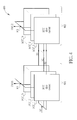
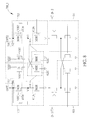
- the input stage 700A, the output buffer 700B and the signal reconstruction circuit 700C of the PCC slice circuit PCC_1 are turned off if the gain setting of the first amplifier circuit 701 for the low-gain mode does not need the PCC slice circuit PCC_1 to be turned on, as illustrated in FIG. 9 .
- the input stage 700A and the output buffer 700B of the PCC slice circuit PCC_1 are turned on and the signal reconstruction circuit 700C of the PCC slice circuit PCC_1 is turned off if the first gain of the first amplifier circuit 701 is equal to the second gain of the second amplifier circuit 702, as illustrated in FIG. 10 .
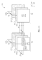
- the input stage 700A and the output buffer 700B of the PCC slice circuit PCC_1 are turned on and the signal reconstruction circuit 700C of the PCC slice circuit PCC_1 is turned off if the first gain of the first amplifier circuit 701 is larger than the second gain of the second amplifier circuit 702, as illustrated in FIG. 11 .
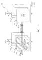
- the output buffer 700B of the PCC slice circuit PCC_1 is turned off and the input stage 700A and the signal reconstruction circuit 700C of the PCC slice circuit PCC_1 are turned on if the first gain of the first amplifier circuit 701 is smaller than the second gain of the second amplifier circuit 702, as illustrated in FIG. 12 .
- the first amplifier circuit 401/701 and the second amplifier circuit 402/702 can be arranged in a symmetric configuration to support NCCA receiving operation in different bands.
- this is for illustrative purposes only, and is not meant to be a limitation of the present invention.
- the second amplifier circuit 402 is not used to receive an RF signal (e.g., IN_2) of a different NCCA band from another RX port, and the transistors M3H and M6H may be omitted from the SCC slice circuit 412.
- an RF signal e.g., IN_2
- the second amplifier circuit 702 is not used to receive an RF signal (e.g., IN_2) of a different NCCA band from another RX port, and the transistors M3H, M6H and T2 may be omitted from the SCC slice circuit 712. These also fall within the scope of the present invention.
- an RF signal e.g., IN_2
- the transistors M3H, M6H and T2 may be omitted from the SCC slice circuit 712.
- the first amplifier circuit 401/701 is composed of PCC slice circuits used to generate the first output signal OUT1 for undergoing down-conversion of PCC channel
- the second amplifier circuit 402/702 is composed of SCC slice circuits used to generate the second output signal OUT2 for undergoing down-conversion of SCC channel, where the gain setting of the first amplifier circuit 401/701 and the gain setting of the second amplifier circuit 402/702 can be adjusted independently.
- each of the first output signal OUT1 and the second output signal OUT2 has PCC channel data and SCC channel data, and the first output signal OUT1 and the second output signal OUT2 are generated under the same amplifier gain setting or different amplifier gain settings, depending upon actual signal reception condition.
- the first amplifier circuit 401/701 may be configured to include slice circuits (i.e., SCC slice circuits) used to generate the first output signal OUT1 for undergoing down-conversion of SCC channel
- the second amplifier circuit 402/702 may be configured to include slice circuits (i.e., PCC slice circuits) used to generate the second output signal OUT2 for undergoing down-conversion of PCC channel.
- slice circuits i.e., SCC slice circuits
- PCC slice circuits slice circuits
- one multi-output LNA architecture is provided to support the in-band non-contiguous carrier aggregation reception , wherein the gains of different amplifier circuits (e.g., PCC LNA circuit and SCC LNA circuit) can be adjusted independently, and an input signal of a second amplifier circuit (which is configured to generate an output signal for undergoing down-conversion of one of PCC channel and SCC channel) is provided by a first amplifier circuit (which is configured to generate an output signal for undergoing down-conversion of the other of PCC channel and SCC channel) according to an RF input received from a desired NCCA band.
- a signal reconstruction circuit is provided to selectively reconstruct an inter-stage signal in the first amplifier circuit.
- the signal reconstruction circuit in the first amplifier circuit can be turned on to reconstruct the inter-stage signal that serves as an input signal of the amplifier circuit.
- the inter-stage signal reconstructed by the signal reconstruction circuit is sensed/received by the second amplifier circuit that has an output buffer turned on for generating an amplified output.
Landscapes
- Engineering & Computer Science (AREA)
- Power Engineering (AREA)
- Computer Networks & Wireless Communication (AREA)
- Signal Processing (AREA)
- Amplifiers (AREA)
Abstract
Description
- The present invention relates to an amplifier, and more particularly, to a low-noise amplifier (LNA) for processing two non-contiguous channels in the same band and a related method according to the pre-characterizing clauses of
claims 1 and 9. - Carrier aggregations (CAs) refer to simultaneous wireless reception of several signal channels corresponding to different frequencies in a Long Term Evolution (LTE) wireless system. Considering an intra-band non-contiguous CA (NCCA) case, there is only one receiving band but two non-contiguous channel. Moreover, the wanted signal level of the two channels may not be equal. Hence, a multi-output LNA capable of receiving one RF input and generating two RF outputs to different mixers for down-conversion of two channels and further support a function of using different gains for generating output signals to different mixers for down conversion is required.
- In view of the above, one objective of the present invention is to provide an amplifier and a related method for processing two non-contiguous channels in the same band, such as one PCC channel and one SCC channel transmitted using an intra-band non-contiguous carrier aggregation scheme.
- According to a first aspect of the present invention, an exemplary amplifier applicable to an intra-band non-contiguous carrier aggregation (NCCA) band is provided. The NCCA band includes at least a primary component carrier (PCC) channel and a secondary component carrier (SCC) channel not adjacent to each other. The exemplary amplifier includes a first amplifier circuit and a second amplifier circuit. The first amplifier circuit is arranged to receive a first input signal and generate a first output signal for undergoing down-conversion of one of the PCC channel and the SCC channel. The second amplifier circuit is arranged to receive at least one second input signal and generate a second output signal for undergoing down-conversion of another of the PCC channel and the SCC channel. The at least one second input signal received by the second amplifier circuit is provided by the first amplifier circuit according to the first input signal.
- According to a second aspect of the present invention, an exemplary method for operating an amplifier applicable to an intra-band non-contiguous carrier aggregation (NCCA) band is provided. The NCCA band includes at least a primary component carrier (PCC) channel and a secondary component carrier (SCC) channel not adjacent to each other. The exemplary method includes: utilizing a first amplifier circuit to receive a first input signal and generate a first output signal for undergoing down-conversion of one of the PCC channel and the SCC channel; providing at least one second input signal to a second amplifier circuit; and utilizing the second amplifier circuit to receive the at least one second input signal and to generate a second output signal for undergoing down-conversion of another of the PCC channel and the SCC channel. The at least one second input signal received by the second amplifier circuit is provided by the first amplifier circuit according to the first input signal.
- In the following, the invention is further illustrated by way of example, taking reference to the accompanying drawings. Thereof
-
FIG. 1 is a diagram illustrating an example of a first conventional carrier aggregation scheme, -
FIG. 2 is a diagram illustrating an example of a second conventional carrier aggregation scheme, -
FIG. 3 is a diagram illustrating an example of a third conventional carrier aggregation scheme, -
FIG. 4 is a diagram illustrating an amplifier according to an embodiment of the present invention, -
FIG. 5 is a diagram illustrating a partial circuit structure of the amplifier shown inFIG. 4 according to an embodiment of the present invention, -
FIG. 6 is a diagram illustrating a case where a gain setting of a first amplifier circuit is smaller than a gain setting of a second amplifier circuit, -
FIG. 7 is a diagram illustrating an amplifier according to another embodiment of the present invention, -
FIG. 8 is a diagram illustrating a partial circuit structure of the amplifier shown inFIG. 7 according to an embodiment of the present invention, -
FIG. 9 is a diagram illustrating the amplifier shown inFIG. 7 that is operated in a first operating status according to an embodiment of the present invention, -
FIG. 10 is a diagram illustrating the amplifier shown inFIG. 7 that is operated in a second operating status according to an embodiment of the present invention, -
FIG. 11 is a diagram illustrating the amplifier shown inFIG. 7 that is operated in a third operating status according to an embodiment of the present invention, and -
FIG. 12 is a diagram illustrating the amplifier shown inFIG. 7 that is operated in a fourth operating status according to an embodiment of the present invention. - Certain terms are used throughout the description and following claims to refer to particular components. As one skilled in the art will appreciate, manufacturers may refer to a component by different names. This document does not intend to distinguish between components that differ in name but not function. In the following description and in the claims, the terms "include" and "comprise" are used in an open-ended fashion, and thus should not be interpreted as a close-ended term such as "consist of". Also, the term "couple" is intended to mean either an indirect or direct electrical connection. Accordingly, if one device is coupled to another device, that connection may be through a direct electrical connection, or through an indirect electrical connection via other devices and connections.
-
FIGs. 1-3 illustrate different carrier aggregation schemes, respectively. The intra-band continuous/non-contiguous carrier aggregation occurs when multiple component carriers locate in a same radio frequency (RF) band, as shown inFIGs. 1 and 2 . The inter-band carrier aggregation occurs when multiple available component carriers locate in different RF bands, as shown inFIG. 3 . - As illustrated in the intra-band
contiguous carrier aggregation 100 ofFIG. 1 , thesignal channels frequency component carrier 102b may be viewed as a primary component carrier (PCC), and the lower-frequency component carrier 102a may be viewed as the secondary component carrier (SCC). -
FIG. 2 illustrates an example of intra-band non-contiguouscarrier aggregation 200, wherein thecomponent carriers frequency component carrier 202b may be viewed as the PCC, and the lower-frequency component carrier 202a may be viewed as the SCC. -
FIG. 3 illustrates an example of inter-bandnon-contiguous carrier aggregation 300, wherein thecomponent carriers component carrier 302a may be the PCC and thecomponent carrier 302b may be the SCC. In the inter-band carrier aggregation shown inFIG. 3 , the two signal channels are in different reception bands. - In
FIG. 2 , there is only one receiving band (Band A) and two non-contiguous channels. Thus, there is a need for an innovative low-noise amplifier (LNA) design which is capable of receiving one RF input and generating two RF outputs to different mixers for down-conversion of two channels, including one PCC channel and one SCC channel. Further, since the required signal levels of the two channels, including one PCC channel and one SCC channel, may not be equal to each other, there is also a need for enabling an LNA design to support a function of using different gains for generating output signals to different mixers for down conversion. -
FIG. 4 is a diagram illustrating anamplifier 400 according to an embodiment of the present invention. In one embodiment, theamplifier 400 is applied to an NCCA band (e.g. the NCCA band shown inFIG. 2 ). In one embodiment, theamplifier 400 is a low noise amplifier (LNA) with multiple outputs. As shown inFIG. 4 , theamplifier 400 includes a first amplifier circuit (e.g., first LNA circuit) 401 and a second amplifier circuit (e.g., second LNA circuit) 402. Thefirst amplifier circuit 401 includes a plurality of first slice circuits (e.g., PCC slice circuits PCC_1-PCC_N), and thesecond amplifier circuit 402 includes a plurality of second slice circuits (e.g., SCC slice circuits SCC_1-SCC_N), where the plurality of PCC slice circuits PCC_1-PCC_N correspond to the plurality of SCC slice circuits SCC_1-SCC_N, respectively. In one embodiment, the PCC slice circuits PCC_1-PCC_N are coupled to the SCC slice circuits SCC_1-SCC_N, respectively. Hence, an input signal of an SCC slice circuit is provided by a corresponding PCC slice circuit. - In this example, the
first amplifier circuit 401 is arranged to receive a first input signal S1 and generate a first output signal OUT1 for undergoing down-conversion of the PCC channel at one mixer (not shown), and thesecond amplifier circuit 402 is arranged to receive at least one second input signal S2 and generate a second output signal OUT2 for undergoing down-conversion of the SCC channel at another mixer (not shown), where the at least one second input signal S2 received by thesecond amplifier circuit 402 is provided by thefirst amplifier circuit 401 according to the first input signal S1. The first input signal S1 is received from an NCCA band. Since each of the first output signal OUT1 and the second output signal OUT2 is derived from amplifying an input signal directly/indirectly set by the first input signal S1, each of the first output signal OUT1 and the second output signal OUT2 include PCC channel components and SCC channel components. - When a PCC slice circuit is turned on, the PCC slice circuit receives the first input signal S1, and amplifies the first input signal S1 to generate an amplified output to an output port N1 of the
first amplifier circuit 401. Hence, amplified outputs generated from turned-on PCC slice circuits are combined at the output port N1 of thefirst amplifier circuit 401 to form the first output signal OUT1 having PCC channel components and SCC channel components. Moreover, thefirst amplifier circuit 401 is arranged to generate the first output signal OUT1 according to a first gain (e.g., PCC gain), where the first gain is adjusted according to the number of turned-on PCC slice circuits of thefirst amplifier circuit 401. As mentioned above, the first output signal OUT1 will undergo down-conversion of the PCC channel. Hence, thefirst amplifier circuit 401 with the first gain properly adjusted can ensure that PCC channel components in the first output signal OUT1 have proper magnitude, such that a down-conversion result of the PCC channel will have desired signal magnitude. - Similarly, when an SCC slice circuit is turned on, the SCC slice circuit receives a second input signal S2 from a corresponding PCC slice circuit, and amplifies the received second input signal S2 to generate an amplified output to an output port N2 of the
second amplifier circuit 402. Hence, amplified outputs generated from turned-on SCC slice circuits are combined at the output port N2 of thesecond amplifier circuit 402 to form the second output signal OUT2 having PCC channel components and SCC channel components. Moreover, thesecond amplifier circuit 402 is arranged to generate the second output signal OUT2 according to a second gain (e.g., SCC gain), where the second gain is adjusted according to the number of turned-on SCC slice circuits of thesecond amplifier circuit 402. As mentioned above, the second output signal OUT2 will undergo down-conversion of the SCC channel. Hence, thesecond amplifier circuit 402 with the second gain properly adjusted can ensure that SCC channel components in the second output signal OUT1 have proper magnitude, such that a down-conversion result of the SCC channel will have desired signal magnitude. - In one exemplary design, the PCC slice circuits PCC_1-PCC_N may include low-gain slice circuits and high-gain slice circuits, and the SCC slice circuits SCC_1-SCC_N may include low-gain slice circuits and high-gain slice circuits. For example, the PCC slice circuit PCC_N and the SCC slice circuit SCC_N shown in
FIG. 4 may be low-gain slice circuits, and the PCC slice circuits PCC_1-PCC_2 and the SCC slice circuits SCC_1-SCC_2 shown inFIG. 4 may be high-gain slice circuits. The high-gain slice circuit and the low-gain slice circuit have different amplifier structures with different gain settings. By way of example, but not limitation, the high-gain slice circuit may employ a shunt-shunt feedback LNA structure. Alternatively, all of the PCC slice circuits PCC_1-PCC_N may be high-gain slice circuits, and all of the SCC slice circuits SCC_1-SCC_N may be high-gain slice circuits. -
FIG. 5 is a diagram illustrating a partial circuit structure 400_1 of theamplifier 400 shown inFIG. 4 according to an embodiment of the present invention. For example, only four slice circuits are shown inFIG. 5 for illustrative purposes. The partial circuit structure 400_1 includes twoPCC slice circuits SCC slice circuits PCC slice circuit 411 and theSCC slice circuit 412 may be high-gain slice circuits for a high-gain path/high-gain mode, and thePCC slice circuit 413 and theSCC slice circuit 414 may be low-gain slice circuits for a low-gain path/low-gain mode. The high-gain path and the low-gain path may be selected/switched according to design requirements. For example, one of a high-gain mode and a low-gain mode may be selected to match a current operation requirement. When the low-gain mode is selected, smaller current consumption may be achieved through using low-gain slice circuit(s) only. However, this is for illustrative purposes only, and is not meant to be a limitation of the present invention. Alternatively, the low-gain slice circuits, such as thePCC slice circuit 413 and theSCC slice circuit 414 shown inFIG. 4 , may be omitted. - The
PCC slice circuit 411 includes anoutput buffer 411B, oneinput stage 411A and anotherinput stage 411C. TheSCC slice circuit 412 includes anoutput buffer 412B, oneinput stage 412A and anotherinput stage 412C. By way of example, rather than limitation, theinput stage 411A may include a transistor M1H, theoutput buffer 411B may include a transistor M2H, theinput stage 411C may include a transistor M6H, theinput stage 412A may include a transistor M3H, theoutput buffer 412B may include a transistor M4H, and theinput stage 412C may include a transistor M5H. In one example, all of the transistors M1H-M6H may be N-channel metal-oxide-semiconductor transistors (NMOS transistors). - In one embodiment, the
first amplifier circuit 401 and thesecond amplifier circuit 402 can be arranged in a symmetric configuration. Hence, the same amplifier circuitry can be shared for performing the NCCA receiving operation in different bands. For example, when a mobile phone using theamplifier 400 is operated in a first region/country, an NCCA band in use may be a first band. A radio frequency (RF) signal (e.g., IN_1) may be received from a first receive (RX) port and fed into theamplifier 400. For another example, when the mobile phone using theamplifier 400 is operated in a second region/country, an NCCA band in use may be a second band different from the first band. An RF signal (e.g., IN_2) may be received from a second RX port and fed into theamplifier 400. For clarity and simplicity, the following assumes that the RF signal (e.g., IN_1) of a desired NCCA band is received from the first RX port and fed into theamplifier 400, while no RF signal (e.g., IN_2) is received from the second RX port. Since a person skilled in the art can readily understand details of processing an RF signal (e.g., IN_2) of a desired NCCA band received from the second RX port and fed into theamplifier 400 after reading following paragraphs directed to an example of processing an RF signal (e.g. , IN_1) of a desired NCCA band received from the first RX port and fed into theamplifier 400, related description is omitted. - With regard to the
PCC slice circuit 411, a control node of the transistor M1H (e.g., gate of NMOS transistor) is arranged to receive one RF signal, a first connection node of the transistor M1H (e.g., drain of NMOS transistor) is coupled to the transistor M2H, and a second connection node of the transistor M1H (e.g., source of NMOS transistor) is coupled to one reference voltage (e.g., ground voltage). The transistors M1H and M2H are arranged in a cascade fashion. With regard to the transistor M2H, a control node (e.g. , gate of NMOS transistor) is arranged to receive a first bias voltage VB1, a first control node (e.g., drain of NMOS transistor) is coupled to the output port N1 of thefirst amplifier circuit 401, and a second connection node (e.g., source of NMOS transistor) is coupled to the first connection node of the transistor M1H. The first bias voltage VB1 is used to control whether thePCC slice circuit 411 is turned on to have contribution to the first output signal OUT1. When the first bias voltage VB1 has a low level, the transistor M2H is turned off, thus blocking thePCC slice circuit 411 from generating an amplified output that will be at least a portion of the first output signal OUT1. When the first bias voltage VB1 has a high level, the transistor M2H is turned on, thus allowing thePCC slice circuit 411 to generate an amplified output that will be at least a portion of the first output signal OUT1. - With regard to the
SCC slice circuit 412, a control node of the transistor M3H (e.g., gate of NMOS transistor) is arranged to receive another RF signal, a first connection node of the transistor M3H (e.g., drain of NMOS transistor) is coupled to the transistor M4H, and a second connection node of the transistor M3H (e.g., source of NMOS transistor) is coupled to the reference voltage (e.g., ground voltage). The transistors M3H and M4H are arranged in a cascade fashion. With regard to the transistor M4H, a control node (e.g., gate of NMOS transistor) is arranged to receive another first bias voltage VB1', a first control node (e.g., drain of NMOS transistor) is coupled to the output port N2 of thesecond amplifier circuit 402, and a second connection node (e.g., source of NMOS transistor) is coupled to the first connection node of the transistor M3H. The first bias voltage VB1' is used to control whether theSCC slice circuit 412 is turned on to have contribution to the second output signal OUT2. When the second bias voltage VB2 has a low level, the transistor M4H is turned off, thus blocking theSCC slice circuit 412 from generating an amplified output that will be at least a portion of the second output signal OUT2. When the second bias voltage VB2 has a high level, the transistor M4H is turned on, thus allowing theSCC slice circuit 412 to generate an amplified output that will be at least a portion of the second output signal OUT2. - Consider a case where the RF signal (e.g., IN_1) of a desired NCCA band is received from the first RX port and fed into the
amplifier 400, while no RF signal (e.g., IN_2) is received from the second RX port. As shown inFIG. 5 , a control node of the transistor M5H (e.g., gate of NMOS transistor) is coupled to the first connection node of the transistor M1H, a first connection node of the transistor M5H (e.g., drain of NMOS transistor) is coupled to the first connection node of the transistor M3H, and a second connection node of the transistor M5H (e.g., source of NMOS transistor) is coupled to the reference voltage (e.g., ground voltage). Since the SCC (e.g. thecomponent carrier 202a mentioned inFIG. 2 ) is located in the same band as PCC in the NCCA scenario in which thePCC slice circuit 411 is turned on by one first bias voltage VB1 and theSCC slice circuit 412 is also turned on by another first bias voltage VB1' , it is a part of the first input signal IN_1 and also received through thePCC slice circuit 411 of thefirst amplifier circuit 401. Therefore, in addition to the PCC signal, the SCC signal is also amplified by theinput stage 411A of thePCC slice circuit 411. Moreover, an inter-stage signal V1 is generated by theinput stage 411A before the amplified output of thePCC slice circuit 411 is output to the output port N1 of thefirst amplifier circuit 401. Though theinput stage 412A of theSCC slice circuit 412 is turned off, theinput stage 412C of theSCC slice circuit 412 is arranged to sense/receive the inter-stage signal V1 as a second input signal, and amplify the second input signal (which is derived from the inter-stage signal VI) to generate a signal V2 to theoutput buffer 412B of theSCC slice circuit 412. It should be noted that theinput stage 411C is turned off in this case. Finally, theoutput buffer 412B generates an amplified output to the output port N2 of thesecond amplifier circuit 402 according to the signal V2 derived from the inter-stage signal V1 via theinput stage 412C. It should be noted that each of the first output signal OUT1 and the second output signal OUT2 has the PCC channel data and the SCC channel data. Hence, one mixer with a local oscillator frequency properly set to the PCC can perform down-conversion to extract the PCC channel data from the first output signal OUT1, and another mixer with a local oscillator frequency properly set to the SCC can perform down-conversion to extract the SCC channel data from the second output signal OUT2. - With regard to the low-gain path in the NCCA scenario, a signal is sensed from an input node of the
PCC slice circuit 413 directly and then fed to a cascade node inside theSCC slice circuit 414 through an input stage when the RF signal (e.g. , IN_1) of a desired NCCA band is received from the first RX port. As low-gain slice circuits can be optional and the present invention focuses on the high-gain slice circuits, further description of the low-gain slice circuits is omitted for brevity. - As mentioned above, the first gain of the
first amplifier circuit 401 is controlled by the number of turned-on PCC slice circuits, and the second gain of thesecond amplifier circuit 402 is controlled by the number of turned-on SCC slice circuits. Considering the high-gain path in the NCCA scenario, if the first gain of thefirst amplifier circuit 401 used to generate the first output signal OUT1 for undergoing down-conversion of the PCC channel is required to be equal to the second gain of thesecond amplifier circuit 402 used to generate the second output signal OUT2 for undergoing down-conversion of the SCC channel, the number of turned-on PCC slice circuits in thefirst amplifier circuit 401 is equal to the number of turned-on SCC slice circuits in thesecond amplifier circuit 402. Hence, both of thePCC slice circuit 411 and theSCC slice circuit 412 are turned on, such that the inter-stage signal V1 can be created in thePCC slice circuit 411 and sensed by theSCC slice circuit 412. However, if the first gain of thefirst amplifier circuit 401 used to generate the first output signal OUT1 for undergoing down-conversion of the PCC channel is required to be smaller than the second gain of thesecond amplifier circuit 402 used to generate the second output signal OUT2 for undergoing down-conversion of the SCC channel, the number of turned-on PCC slice circuits in thefirst amplifier circuit 401 is smaller than the number of turned-on SCC slice circuits in thesecond amplifier circuit 402. Hence, it is possible that thePCC slice circuit 411 should be turned off, and theSCC slice circuit 412 should be turned on. In this case, there is an issue that theSCC slice circuit 412 is unable to generate the second output signal OUT2 due to the turned-offPCC slice circuit 411. This phenomenon is illustrated inFIG. 6 . -
FIG. 6 is a diagram illustrating a case where the first gain of thefirst amplifier circuit 401 is smaller than the second gain of thesecond amplifier circuit 402. In this example, one first bias voltage VB1 is set by a low level for turning off the PCC slice circuit 411 (particularly, theoutput buffer 411B coupled to the output port N1), and another first bias voltage VB1' is set by a high level for turning on the SCC slice circuit 412 (particularly, theoutput buffer 412B coupled to the output port N2). Since the first bias voltage VB1 is a low level to the gate of the transistor M2H of theoutput buffer 411B, the transistor M2H is turned off. Since the current path of the cascoded transistors M1H and M2H is cut off due to the turned-off transistor M2H, no inter-stage signal V1 is created at the cascade node in thePCC slice circuit 411. As a result, no inter-stage signal V1 can be sensed by theinput stage 412C to generate the signal V2 at the cascade node between the transistors M3H and M4H. Hence, theSCC slice circuit 412 is unable to generate an amplified output to the output port N2 of thesecond amplifier circuit 402 due to absence of a second input signal provided by thePCC slice circuit 411. It should be noted that, in addition to the transistor M2H, the transistors M3H and M6H are also turned off in this case. - To solve the above issue encountered in the case shown in
FIG. 6 , a solution is provided inFIG. 7. FIG. 7 is a diagram illustrating anamplifier 700 according to another embodiment of the present invention. In one embodiment, theamplifier 700 is applied to an NCCA band (e.g. the NCCA band shown inFIG. 2 ). In one embodiment, theamplifier 700 is a low noise amplifier (LNA) with multiple outputs. As shown inFIG. 7 , theamplifier 700 includes a first amplifier circuit (e.g., first LNA circuit) 701 and a second amplifier circuit (e.g., second LNA circuit) 702. Like thefirst amplifier circuit 401, thefirst amplifier circuit 701 includes a plurality of first slice circuits (e.g., PCC slice circuits PCC_1-PCC_N). Like thesecond amplifier circuit 402, thesecond amplifier circuit 702 includes a plurality of second slice circuits (e.g., SCC slice circuits SCC_1-SCC_N), where the plurality of PCC slices PCC_1-PCC_N correspond to the plurality of SCC slices SCC_1-SCC_N, respectively. In one embodiment, the PCC slice circuits PCC_1-PCC_N are coupled to the SCC slice circuits SCC_1-SCC_N, respectively. Hence, an input signal of an SCC slice circuit is provided by a corresponding PCC slice circuit. - The
first amplifier circuit 701 is used to generate a first output signal OUT1 at an output port N1 for undergoing down-conversion of the PCC channel at one mixer (not shown), and thesecond amplifier circuit 702 is used to generate a second output signal OUT2 at an output port N2 for undergoing down-conversion of the SCC channel at another mixer (not shown). In one exemplary design, the PCC slice circuits PCC_1-PCC_N of thefirst amplifier circuit 701 may include low-gain slice circuits and high-gain slice circuits, and the SCC slice circuits SCC_SCC_N of thesecond amplifier circuit 702 may include low-gain slice circuits and high-gain slice circuits. In another exemplary design, the PCC slice circuits PCC_1-PCC_N of thefirst amplifier circuit 701 may include high-gain slice circuits only, and the SCC slice circuits SCC_1-SCC_N of thesecond amplifier circuit 702 may include high-gain slice circuits. As shown inFIG. 7 , the PCC slice circuit PCC_1 and the SCC slice circuit SCC_1 are high-gain slice circuit. By way of example, but not limitation, the high-gain slice circuit may employ a shunt-shunt feedback LNA structure. - The slice-based structure and associated gain control operation of the
amplifier 700 are similar to that of theamplifier 400. The major difference between theamplifiers first amplifier circuit 701 and thesecond amplifier circuit 702 can be arranged in a symmetric configuration (the RF input of 702 and its signal path is not shown in the Figure for simplification). Hence, the same amplifier circuitry can be shared for performing the NCCA receiving operation in different bands. For example, the PCC slice circuit PCC_1 includes at least aninput stage 700A, anoutput buffer 700B and asignal reconstruction circuit 700C, and the SCC slice circuit SCC_1 includes at least aninput stage 710A, anoutput buffer 710B and asignal reconstruction circuit 710C. - In a case where an RF signal received from a desired NCCA band is fed into the
first amplifier circuit 701 as illustrated inFIG. 7 , thesignal reconstruction circuit 700C can be used to reconstruct a second input signal S2 provided from the PCC slice circuit PCC_1 to the corresponding SCC slice circuit SCC_1 when theoutput buffer 700B should be turned off and theoutput buffer 710B should be turned on. Hence, in one high-gain PCC slice circuit (e.g. the PCC slice circuit PCC_1), if theoutput buffer 700B is turned off, thesignal reconstruction circuit 700C of this PCC slice circuit will be turned on to avoid the situation that no inter-stage signal is available at a cascade node of the PCC slice circuit. In other words, thesignal reconstruction circuit 700C can ensure that the second input signal S2 is delivered to a corresponding SCC slice circuit (e.g. SCC slice circuit SCC_1) from the PCC slice circuit (e.g. PCC slice PCC_1) when theoutput buffer 700B is off, to make the corresponding SCC slice circuit remain functional for generating an amplified output to the output port N2 of thesecond amplifier circuit 702. - The
first amplifier circuit 701 and thesecond amplifier circuit 702 can be arranged in a symmetric configuration. In another case where an RF signal received from a desired NCCA band is fed into thesecond amplifier circuit 702, thesignal reconstruction circuit 710C can be used to reconstruct an input signal provided from the SCC slice circuit SCC_1 to the corresponding PCC slice circuit PCC_1 when theoutput buffer 710B should be turned off and theoutput buffer 700B should be turned on. Hence, in one high-gain SCC slice circuit (e.g. SCC slice circuit SCC_1), if theoutput buffer 710B is turned off, thesignal reconstruction circuit 710C of this SCC slice circuit will be turned on to avoid the situation that no inter-stage signal is available at a cascade node of the SCC slice circuit. In other words, thesignal reconstruction circuit 710C can ensure an input signal is delivered to a corresponding PCC slice circuit (e.g. PCC slice circuit PCC_1) from the SCC slice circuit SCC_1 when theoutput buffer 710B is off, to make the corresponding PCC slice circuit remain functional for generating an amplified output to the output port N1 of thefirst amplifier circuit 701. -
FIG. 8 is a diagram illustrating a partial circuit structure 700_1 of theamplifier 700 shown inFIG. 7 according to an embodiment of the present invention. The partial circuit structure 700_1 can be obtained by adding twosignal reconstruction circuits FIG. 4 . In this embodiment, only four slice circuits are shown inFIG. 8 for illustrative purposes. The partial circuit structure 700_1 includes twoPCC slice circuits SCC slice circuits PCC slice circuit 711 and theSCC slice circuit 712 may be high-gain slice circuits for the high-gain path/high-gain mode, and thePCC slice circuit 413 and theSCC slice circuit 414 may be low-gain slice circuits for the low-gain path/low-gain mode. ThePCC slice circuit 711 includes thesignal reconstruction circuit 717 and the aforementioned input stages 411A, 411C andoutput buffer 411B. TheSCC slice circuit 712 includes thesignal reconstruction circuit 718 and the aforementioned input stages 412A, 412C andoutput buffer 412B. If the PCC slice circuit PCC_1 inFIG. 7 is implemented using thePCC slice circuit 711 and the corresponding SCC slice circuit SCC_1 inFIG. 7 is implemented using theSCC slice circuit 712, theinput stage 700A is implemented using theinput stage 411A, theoutput buffer 700B is implemented using theoutput buffer 411B, thesignal reconstruction circuit 700C is implemented using thesignal reconstruction circuit 717, theinput stage 710A is implemented using theinput stage 412A, theoutput buffer 710B is implemented using theoutput buffer 412B, and thesignal reconstruction circuit 710C is implemented using thesignal reconstruction circuit 718. - In this embodiment, the
signal reconstruction circuit 717 includes a transistor (e.g., NMOS transistor) T1, and thesignal reconstruction circuit 718 includes a transistor (e.g., NMOS transistor) T2. With regard to the transistor T1, a control node (e.g., gate of NMOS transistor) is arranged to receive a second bias voltage VB2, a first connection node (e.g., drain of NMOS transistor) is coupled to another reference voltage (e.g., supply voltage VDD), and a second connection node (e. g. , source of NMOS transistor) is connected to the first connection node of the transistor M1H. The second bias voltage VB2 is used to control whether thesignal reconstruction circuit 717 is turned on to reconstruct an inter-stage signal V1 at a cascode node between the transistors M1H and M2H. With regard to the transistor T2, a control node (e.g., gate of NMOS transistor) is arranged to receive another second bias voltage VB2', a first connection node (e.g., drain of NMOS transistor) is coupled to another reference voltage (e.g., supply voltage VDD), and a second connection node (e.g., source of NMOS transistor) is connected to the first connection node of the transistor M3H. The second bias voltage VB2' is used to control whether thesignal reconstruction circuit 718 is turned on to reconstruct an inter-stage signal V2 at a cascode node between the transistors M3H and M4H. - It should be noted that an inter-stage signal V1 is sensed/received by the
input stage 412C to generate a signal V2 at the cascade node between the transistors M3H and M4H when the RF signal (e.g., IN_1) received from a desired NCCA band is fed into thefirst amplifier circuit 701, and an inter-stage signal V2 is sensed/received by theinput stage 411C to generate a signal V1 at the cascade node between the transistors M1H and M2H when the RF signal (e.g., IN_2) received from a desired NCCA band is fed into thesecond amplifier circuit 702. For clarity and simplicity, the following assumes that the RF signal (e.g., IN_1) of a desired NCCA band is received from a first RX port and fed into theamplifier 700, while no RF signal (e.g., IN_2) is received from a second RX port. - The first gain of the
first amplifier circuit 701 is controlled by the number of turned-on PCC slice circuits, and the second gain of thesecond amplifier circuit 702 is controlled by the number of turned-on SCC slice circuits. Considering the high-gain path in the NCCA scenario, if the first gain of thefirst amplifier circuit 701 used to generate the first output signal OUT1 for undergoing down-conversion of the PCC channel is required to be smaller than the second gain of thesecond amplifier circuit 702 used to generate the second output signal OUT2 for undergoing down-conversion of the SCC channel, the number of turned-on PCC slice circuits in thefirst amplifier circuit 701 is smaller than the number of turned-on SCC slice circuits in thesecond amplifier circuit 702. If the gain setting of thefirst amplifier circuit 701 requires thePCC slice circuit 711 shown inFIG. 8 to be turned off, and the gain setting of thesecond amplifier circuit 702 requires theSCC slice circuit 712 shown inFIG. 8 to be turned on, the first bias voltage VB1 is set by a low level, and another first bias voltage VB1' is set by a high level. Since theoutput buffer 411B is turned off due to the transistor M2H turned off by the first bias voltage VB1, the second bias voltage VB2 is set by a high level to turn on the transistor T1 for signal reconstruction. Since thesignal reconstruction circuit 711 is turned on, a current path is established by the transistors M1H and T1, thereby creating the inter-stage signal V1 at the cascode node between the transistors M1H and T1. In other words, thesignal reconstruction circuit 717 is turned on to reconstruct the inter-stage signal V1 that serves as a second input signal sensed/received by the transistor M5H of theinput stage 412C. Though theoutput buffer 411B is turned off without generating an amplified output to the output node N1 of thefirst amplifier circuit 701, the signal V2 is generated at the cascode node between transistors M3H and M4H according to the inter-stage signal V1 reconstructed due to thesignal reconstruction circuit 711. In this way, theoutput buffer 412B of theSCC slice circuit 712 successfully outputs an amplified output to the output node N2 of thesecond amplifier circuit 702 under a condition that theoutput buffer 411B of thePCC slice circuit 711 is turned off. It should be noted that the transistors T2, M3H and M6H are turned off in this case. - The
signal reconstruction circuit 700C will be turned on if necessary. For example, theoutput buffer 700B and thesignal reconstruction circuit 700C are not turned on concurrently. In practice, on/off statuses of input stage, output buffer and signal reconstruction circuit in the proposed high-gain slice circuit depend on the operational status of theamplifier 700. For example, considering a case where theamplifier 700 is operated in a non-NCCA scenario, theinput stage 700A, theoutput buffer 700B and thesignal reconstruction circuit 700C of the PCC slice circuit PCC_1 are turned off if the gain setting of thefirst amplifier circuit 701 for the low-gain mode does not need the PCC slice circuit PCC_1 to be turned on, as illustrated inFIG. 9 . - For another example, considering a case where the
amplifier 700 is operated in an NCCA scenario for processing PCC channel and SCC channel in the same band, theinput stage 700A and theoutput buffer 700B of the PCC slice circuit PCC_1 are turned on and thesignal reconstruction circuit 700C of the PCC slice circuit PCC_1 is turned off if the first gain of thefirst amplifier circuit 701 is equal to the second gain of thesecond amplifier circuit 702, as illustrated inFIG. 10 . - For another example, considering a case where the
amplifier 700 is operated in an NCCA scenario for processing PCC channel and SCC channel in the same band, theinput stage 700A and theoutput buffer 700B of the PCC slice circuit PCC_1 are turned on and thesignal reconstruction circuit 700C of the PCC slice circuit PCC_1 is turned off if the first gain of thefirst amplifier circuit 701 is larger than the second gain of thesecond amplifier circuit 702, as illustrated inFIG. 11 . - For another example, considering a case where the
amplifier 700 is operated in an NCCA scenario for processing PCC channel and SCC channel in the same band, theoutput buffer 700B of the PCC slice circuit PCC_1 is turned off and theinput stage 700A and thesignal reconstruction circuit 700C of the PCC slice circuit PCC_1 are turned on if the first gain of thefirst amplifier circuit 701 is smaller than the second gain of thesecond amplifier circuit 702, as illustrated inFIG. 12 . - In above embodiments, the
first amplifier circuit 401/701 and thesecond amplifier circuit 402/702 can be arranged in a symmetric configuration to support NCCA receiving operation in different bands. However, this is for illustrative purposes only, and is not meant to be a limitation of the present invention. In an alternative design of the partial circuit structure 400_1 shown inFIG. 5 , thesecond amplifier circuit 402 is not used to receive an RF signal (e.g., IN_2) of a different NCCA band from another RX port, and the transistors M3H and M6H may be omitted from theSCC slice circuit 412. In an alternative design of the partial circuit structure 700_1 shown inFIG. 8 , thesecond amplifier circuit 702 is not used to receive an RF signal (e.g., IN_2) of a different NCCA band from another RX port, and the transistors M3H, M6H and T2 may be omitted from theSCC slice circuit 712. These also fall within the scope of the present invention. - In above embodiments, the
first amplifier circuit 401/701 is composed of PCC slice circuits used to generate the first output signal OUT1 for undergoing down-conversion of PCC channel, and thesecond amplifier circuit 402/702 is composed of SCC slice circuits used to generate the second output signal OUT2 for undergoing down-conversion of SCC channel, where the gain setting of thefirst amplifier circuit 401/701 and the gain setting of thesecond amplifier circuit 402/702 can be adjusted independently. It should be noted that each of the first output signal OUT1 and the second output signal OUT2 has PCC channel data and SCC channel data, and the first output signal OUT1 and the second output signal OUT2 are generated under the same amplifier gain setting or different amplifier gain settings, depending upon actual signal reception condition. Hence, in an alternative design, thefirst amplifier circuit 401/701 may be configured to include slice circuits (i.e., SCC slice circuits) used to generate the first output signal OUT1 for undergoing down-conversion of SCC channel, and thesecond amplifier circuit 402/702 may be configured to include slice circuits (i.e., PCC slice circuits) used to generate the second output signal OUT2 for undergoing down-conversion of PCC channel. This also falls within the scope of the present invention. - To summarize, according to the embodiments of the present invention, one multi-output LNA architecture is provided to support the in-band non-contiguous carrier aggregation reception , wherein the gains of different amplifier circuits (e.g., PCC LNA circuit and SCC LNA circuit) can be adjusted independently, and an input signal of a second amplifier circuit (which is configured to generate an output signal for undergoing down-conversion of one of PCC channel and SCC channel) is provided by a first amplifier circuit (which is configured to generate an output signal for undergoing down-conversion of the other of PCC channel and SCC channel) according to an RF input received from a desired NCCA band. Further, a signal reconstruction circuit is provided to selectively reconstruct an inter-stage signal in the first amplifier circuit. For example, when an output buffer in the first amplifier is turned off under a condition that a first gain of the first amplifier circuit is smaller than a second gain of the second amplifier circuit, the signal reconstruction circuit in the first amplifier circuit can be turned on to reconstruct the inter-stage signal that serves as an input signal of the amplifier circuit. Hence, the inter-stage signal reconstructed by the signal reconstruction circuit is sensed/received by the second amplifier circuit that has an output buffer turned on for generating an amplified output.
Claims (15)
- An amplifier (400, 700) applicable to an intra-band non-contiguous carrier aggregation band, hereinafter NCCA band, including at least a primary component carrier channel, hereinafter PCC channel, and a secondary component carrier channel, hereinafter SCC channel, not adjacent to each other, characterized by:a first amplifier circuit (401, 701), arranged to receive a first input signal (S1) and generate a first output signal (OUT1) for undergoing down-conversion of one of the PCC channel and the SCC channel; anda second amplifier circuit (402, 702), arranged to receive at least one second input signal (S2) and generate a second output signal (OUT2) for undergoing down-conversion of another of the PCC channel and the SCC channel;wherein the at least one second input signal (S2) received by the second amplifier circuit (402, 702) is provided by the first amplifier circuit (401, 701) according to the first input signal (S1).
- The amplifier (400, 700) of claim 1, characterized in that the first amplifier circuit (401, 701) comprises:a first slice circuit (PCC_1, PCC_2, PCC_N), comprising:an input stage (411A, 700A), arranged to receive the first input signal (S1); andan output buffer (411B, 700B), coupled to the input stage (411A, 700A) and arranged to output a first amplified output to an output port (N1) of the first amplifier circuit (401, 701), wherein the first amplified output is at least a portion of the first output signal (OUT1) generated at the output port (N1) of the first amplifier circuit (401, 701) when being output from the first slice circuit (PCC_1, PCC_2, PCC_N).
- The amplifier (400, 700) of claim 2, characterized in that the first slice circuit (PCC_1, PCC_2, PCC_N) further comprises:a signal reconstruction circuit (700C, 717), coupled to the input stage (411A, 700A) and arranged to selectively reconstruct the second input signal (S2) provided to the first slice circuit (PCC_1, PCC_2, PCC_N).
- The amplifier (400, 700) of claim 3, characterized in that the output buffer (411B, 700B) and the signal reconstruction circuit (700C, 717) are not turned on concurrently.
- The amplifier (400, 700) of claim 3, characterized in that:the input stage (411A, 700A) comprises:a first transistor (M1H), having a control node arranged to receive the first input signal (S1), a first connection node, and a second connection node coupled to a first reference voltage (VB1), wherein the at least one second input signal (S2) is sensed from the first connection node of the first transistor (M1H);the output buffer (411B, 700B) comprises:a second transistor (M2H), having a control node arranged to receive a first bias voltage, a first connection node coupled to the output port (N1) of the first amplifier circuit (401, 701), and a second connection node coupled to the first connection node of the first transistor (M1H); andthe signal reconstruction circuit (700C, 717) comprises:a third transistor (T1), having a control node arranged to receive a second bias voltage (VB2), a first connection node coupled to a second reference voltage (VB2), and a second connection node coupled to the first connection node of the first transistor (M1H).
- The amplifier (400, 700) of claim 3, characterized in that the second amplifier circuit (402, 702) comprises:a second slice circuit (SCC_1, SCC_2, SCC_N), arranged to receive a second input signal (S2) from the first slice circuit (PCC_1, PCC_2, PCC_N), and output a second amplified signal to an output port (N2) of the second amplifier circuit (402, 702), wherein the second amplified signal is at least a portion of the second output signal generated at the output port (N2) of the second amplifier circuit (402, 702) when being output from the second slice circuit.
- The amplifier of claim 6, characterized in that the first amplifier circuit (401, 701) comprises a plurality of first slice circuits (PCC_1, PCC_2, PCC_N), including the first slice circuit (PCC_1, PCC_2, PCC_N); the second amplifier circuit (402, 702) comprises a plurality of second slice circuits (SCC_1, SCC_2, SCC_N), including the second slice circuit (SCC_1, SCC_2, SCC_N); the first amplifier circuit (401, 701) is arranged to generate the first output signal (OUT1) according to a first gain; the second amplifier circuit (402, 702) is arranged to generate the second output signal (OUT2) according to a second gain; the first gain is adjusted according to a number of turned-on first slice circuits of the first amplifier circuit (401, 701); and the second gain is adjusted according to a number of turned-on second slice circuits (SCC_1, SCC_2, SCC_N) of the second amplifier circuit (402, 702).
- The amplifier (400, 700) of claim 7, characterized in that the first gain and the second gain are adjusted independently, or when the first gain is smaller than the second gain, the output buffer (411B) is turned off, and the signal reconstruction circuit (700C, 717) is turned on to reconstruct the second input signal (S2), or when the first gain is not smaller than the second gain, the output buffer (411B) is turned on to enable generation of the second input signal (S2), and the signal reconstruction circuit (700C, 717) is turned off.
- A method for operating an amplifier (400, 700) applicable to an intra-band non-contiguous carrier aggregation band, hereinafter NCCA band, including at least a primary component carrier channel, hereinafter PCC channel, and a secondary component carrier channel, hereinafter SCC channel, not adjacent to each other, characterized by::utilizing a first amplifier circuit (401, 701) to receive a first input signal (S1) and generate a first output signal (OUT1) for undergoing down-conversion of one of the PCC channel and the SCC channel;providing at least one second input signal (S2) to a second amplifier circuit (402, 702); andutilizing the second amplifier circuit (402, 702) to receive the at least one second input signal (S2) and to generate a second output signal (OUT2) for undergoing down-conversion of another of the PCC channel and the SCC channel;wherein the at least one second input signal (S2) received by the second amplifier circuit (402, 702) is provided by the first amplifier circuit (401, 701) according to the first input signal (S1).
- The method of claim 9, characterized in that utilizing the first amplifier circuit (401, 701) comprises:utilizing a first slice circuit (PCC_1, PCC_2, PCC_N), comprising:utilizing an input stage (411A, 700A) to receive the first input signal (S1); andutilizing an output buffer (411B, 700B), coupled to the input stage (411A, 700A), to output a first amplified output to an output port (N1) of the first amplifier circuit (401, 701), wherein the first amplified output is at least a portion of the first output signal (OUT1) generated at the output port (N1) of the first amplifier circuit (401, 701) when being output from the first slice circuit (PCC_1, PCC_2, PCC_N).
- The method of claim 10, characterized in that utilizing the first slice circuit (PCC_1, PCC_2, PCC_N) further comprises:utilizing a signal reconstruction circuit 9700C, 717), coupled to the input stage (411A, 700A), to selectively reconstruct the second input signal (S2) provided to the first slice circuit (PCC_1, PCC_2, PCC_N).
- The method of claim 11, characterized in that the output buffer (411B, 700B) and the signal reconstruction circuit (700C, 717) are not turned on concurrently.
- The method of claim 11, characterized in that:the input stage (411A, 700A) comprises:a first transistor (M1H), having a control node arranged to receive the first input signal (S1), a first connection node, and a second connection node coupled to a first reference voltage, wherein the at least one second input signal (S1) is sensed from the first connection node of the first transistor (M1H);the output buffer (411B, 700B) comprises:a second transistor (M2H), having a control node arranged to receive a first bias voltage (VB1), a first connection node coupled to the output port (N1) of the first amplifier circuit (401, 701), and a second connection node coupled to the first connection node of the first transistor (M1H); andthe signal reconstruction circuit (700C, 717) comprises:a third transistor (T1), having a control node arranged to receive a second bias voltage (VB2), a first connection node coupled to a second reference voltage (VB2), and a second connection node coupled to the first connection node of the first transistor (M1H).
- The method of claim 11, characterized in that utilizing the second amplifier circuit (402, 702) comprises:utilizing a second slice circuit (SCC_1, SCC_2, SCC_N) to receive a second input signal (S2) from the first slice circuit (PCC_1, PCC_2, PCC_N) and to output a second amplified signal to an output port (N2) of the second amplifier circuit (402, 702), wherein the second amplified signal is at least a portion of the second output signal (OUT2) generated at the output port (N2) of the second amplifier circuit (402, 702) when being output from the second slice circuit (SCC_1, SCC_2, SCC_N).
- The method of claim 14, characterized in that the first amplifier circuit (401, 701) comprises a plurality of first slice circuits (PCC_1, PCC_2, PCC_N), including the first slice circuit (PCC_1, PCC_2, PCC_N); the second amplifier circuit (402, 702) comprises a plurality of second slice circuits (SCC_1, SCC_2, SCC_N), including the second slice circuit (SCC_1, SCC_2, SCC_N); the first amplifier circuit (401, 701) is arranged to generate the first output signal (OUT1) according to a first gain; the second amplifier circuit (402, 702) is arranged to generate the second output signal (OUT2) according to a second gain; and the method further comprises:adjusting the first gain according to a number of turned-on first slice circuits (PCC_1, PCC_2, PCC_N) of the first amplifier circuit (401, 701); andadjusting the second gain according to a number of turned-on second slice circuits (SCC_1, SCC_2, SCC_N) of the second amplifier circuit (402, 702).
Applications Claiming Priority (2)
| Application Number | Priority Date | Filing Date | Title |
|---|---|---|---|
| US201462080933P | 2014-11-17 | 2014-11-17 | |
| US14/922,208 US9641139B2 (en) | 2014-11-17 | 2015-10-26 | Amplifier and related method |
Publications (2)
| Publication Number | Publication Date |
|---|---|
| EP3021483A1 true EP3021483A1 (en) | 2016-05-18 |
| EP3021483B1 EP3021483B1 (en) | 2020-07-01 |
Family
ID=54364157
Family Applications (1)
| Application Number | Title | Priority Date | Filing Date |
|---|---|---|---|
| EP15192244.0A Active EP3021483B1 (en) | 2014-11-17 | 2015-10-30 | Amplifier and related method |
Country Status (3)
| Country | Link |
|---|---|
| US (1) | US9641139B2 (en) |
| EP (1) | EP3021483B1 (en) |
| CN (1) | CN105610406B (en) |
Cited By (1)
| Publication number | Priority date | Publication date | Assignee | Title |
|---|---|---|---|---|
| GB2628127A (en) * | 2023-03-14 | 2024-09-18 | Nordic Semiconductor Asa | Amplifiers |
Families Citing this family (2)
| Publication number | Priority date | Publication date | Assignee | Title |
|---|---|---|---|---|
| US10033337B2 (en) | 2016-08-09 | 2018-07-24 | Qualcomm Incorporated | Multi-stage bandpass low-noise amplifier |
| US12022448B2 (en) | 2017-08-11 | 2024-06-25 | Qualcomm Incorporated | Carrier switching for multiple carriers using the same components of a component path |
Citations (6)
| Publication number | Priority date | Publication date | Assignee | Title |
|---|---|---|---|---|
| US20100182090A1 (en) * | 2009-01-19 | 2010-07-22 | Zixiang Yang | Ultra low noise high linearity lna for multi-mode transceiver |
| US20100237945A1 (en) * | 2009-03-19 | 2010-09-23 | Qualcomm Incorporated | Cascode amplifier with protection circuitry |
| US20130315348A1 (en) * | 2012-05-25 | 2013-11-28 | Qualcomm Incorporated | Low noise amplifiers for carrier aggregation |
| US20140213209A1 (en) * | 2013-01-25 | 2014-07-31 | Qualcomm Incorporated | Single-input multiple-output amplifiers with independent gain control per output |
| US20140210554A1 (en) * | 2013-01-25 | 2014-07-31 | Qualcomm Incorporated | Amplifiers with improved isolation |
| US20140253242A1 (en) * | 2013-03-11 | 2014-09-11 | Qualcomm Incorporated | Amplifiers with inductive degeneration and configurable gain and input matching |
Family Cites Families (7)
| Publication number | Priority date | Publication date | Assignee | Title |
|---|---|---|---|---|
| EP1332562B1 (en) * | 2000-11-03 | 2007-10-24 | QUALCOMM Incorporated | Apparatus for reducing phase noise in a local carrier signal caused by powering down of circuit elements during discontinuous data transmissions |
| US7120411B2 (en) | 2002-03-25 | 2006-10-10 | Broadcom Corporation | Low noise amplifier (LNA) gain switch circuitry |
| US7486135B2 (en) | 2007-05-29 | 2009-02-03 | Telefonaktiebolaget Lm Ericsson (Publ) | Configurable, variable gain LNA for multi-band RF receiver |
| US8412139B2 (en) * | 2011-01-10 | 2013-04-02 | Telefonaktiebolaget L M Ericsson (Publ) | Methods of receiving multiple carriers using different RF mixer frequencies and related communications devices and receivers |
| US8698560B2 (en) | 2012-05-09 | 2014-04-15 | Mstar Semiconductor, Inc. | Variable-gain low noise amplifier |
| US9338668B2 (en) * | 2012-11-07 | 2016-05-10 | Qualcomm Incorporated | Gain control for intra-band carrier aggregation |
| US9362975B2 (en) * | 2014-08-29 | 2016-06-07 | Samsung Electronics Co., Ltd. | Low noise amplifier and method for carrier aggregation and non-carrier aggregation |
-
2015
- 2015-10-26 US US14/922,208 patent/US9641139B2/en active Active
- 2015-10-30 EP EP15192244.0A patent/EP3021483B1/en active Active
- 2015-11-13 CN CN201510777465.2A patent/CN105610406B/en active Active
Patent Citations (6)
| Publication number | Priority date | Publication date | Assignee | Title |
|---|---|---|---|---|
| US20100182090A1 (en) * | 2009-01-19 | 2010-07-22 | Zixiang Yang | Ultra low noise high linearity lna for multi-mode transceiver |
| US20100237945A1 (en) * | 2009-03-19 | 2010-09-23 | Qualcomm Incorporated | Cascode amplifier with protection circuitry |
| US20130315348A1 (en) * | 2012-05-25 | 2013-11-28 | Qualcomm Incorporated | Low noise amplifiers for carrier aggregation |
| US20140213209A1 (en) * | 2013-01-25 | 2014-07-31 | Qualcomm Incorporated | Single-input multiple-output amplifiers with independent gain control per output |
| US20140210554A1 (en) * | 2013-01-25 | 2014-07-31 | Qualcomm Incorporated | Amplifiers with improved isolation |
| US20140253242A1 (en) * | 2013-03-11 | 2014-09-11 | Qualcomm Incorporated | Amplifiers with inductive degeneration and configurable gain and input matching |
Cited By (1)
| Publication number | Priority date | Publication date | Assignee | Title |
|---|---|---|---|---|
| GB2628127A (en) * | 2023-03-14 | 2024-09-18 | Nordic Semiconductor Asa | Amplifiers |
Also Published As
| Publication number | Publication date |
|---|---|
| US20160142027A1 (en) | 2016-05-19 |
| CN105610406B (en) | 2019-04-26 |
| CN105610406A (en) | 2016-05-25 |
| US9641139B2 (en) | 2017-05-02 |
| EP3021483B1 (en) | 2020-07-01 |
Similar Documents
| Publication | Publication Date | Title |
|---|---|---|
| US9271239B2 (en) | Current-efficient low noise amplifier (LNA) | |
| KR102945627B1 (en) | Low noise amplifier for carrier aggregation and apparatus including the same | |
| CN104335483B (en) | Multiple-Input Multiple-Output (MIMO) Low Noise Amplifier for Carrier Aggregation | |
| CA2947886C (en) | Carrier aggregation amplifier with dual gain control | |
| US9723560B2 (en) | Multi-stage amplifier with RC network | |
| JP5666985B2 (en) | Downconverter, downconverter IC, and downconverter control method | |
| EP3021483B1 (en) | Amplifier and related method | |
| EP3134966B1 (en) | Differential cascode amplifier with selectively coupled gate terminals | |
| US9642166B2 (en) | Cross-connected cascode low noise amplifier for carrier aggregation | |
| JP6686016B2 (en) | Receiver front-end architecture for in-band carrier aggregation | |
| US20160173145A1 (en) | Low noise amplifier providing variable gains and noise cancellation for carrier aggregation | |
| US11418156B2 (en) | Low noise amplifier with improved linearity in low gain mode | |
| US9467104B2 (en) | Single-input multiple-output amplifiers with simultaneous multiple gain modes | |
| US9130529B2 (en) | Area-efficient degenerative inductance for a low noise amplifier (LNA) | |
| JP2010268296A (en) | Satellite broadcast receiving converter IC, satellite broadcast receiving converter, and satellite broadcast receiving antenna | |
| EP3355472A1 (en) | Integrated circuit for a transceiver |
Legal Events
| Date | Code | Title | Description |
|---|---|---|---|
| PUAI | Public reference made under article 153(3) epc to a published international application that has entered the european phase |
Free format text: ORIGINAL CODE: 0009012 |
|
| AK | Designated contracting states |
Kind code of ref document: A1 Designated state(s): AL AT BE BG CH CY CZ DE DK EE ES FI FR GB GR HR HU IE IS IT LI LT LU LV MC MK MT NL NO PL PT RO RS SE SI SK SM TR |
|
| AX | Request for extension of the european patent |
Extension state: BA ME |
|
| 17P | Request for examination filed |
Effective date: 20160722 |
|
| RBV | Designated contracting states (corrected) |
Designated state(s): AL AT BE BG CH CY CZ DE DK EE ES FI FR GB GR HR HU IE IS IT LI LT LU LV MC MK MT NL NO PL PT RO RS SE SI SK SM TR |
|
| STAA | Information on the status of an ep patent application or granted ep patent |
Free format text: STATUS: EXAMINATION IS IN PROGRESS |
|
| 17Q | First examination report despatched |
Effective date: 20170118 |
|
| GRAP | Despatch of communication of intention to grant a patent |
Free format text: ORIGINAL CODE: EPIDOSNIGR1 |
|
| STAA | Information on the status of an ep patent application or granted ep patent |
Free format text: STATUS: GRANT OF PATENT IS INTENDED |
|
| INTG | Intention to grant announced |
Effective date: 20200323 |
|
| GRAS | Grant fee paid |
Free format text: ORIGINAL CODE: EPIDOSNIGR3 |
|
| GRAA | (expected) grant |
Free format text: ORIGINAL CODE: 0009210 |
|
| STAA | Information on the status of an ep patent application or granted ep patent |
Free format text: STATUS: THE PATENT HAS BEEN GRANTED |
|
| AK | Designated contracting states |
Kind code of ref document: B1 Designated state(s): AL AT BE BG CH CY CZ DE DK EE ES FI FR GB GR HR HU IE IS IT LI LT LU LV MC MK MT NL NO PL PT RO RS SE SI SK SM TR |
|
| RIN1 | Information on inventor provided before grant (corrected) |
Inventor name: CHOU, CHUNG-YUN Inventor name: YU, CHI-YAO |
|
| REG | Reference to a national code |
Ref country code: CH Ref legal event code: EP Ref country code: AT Ref legal event code: REF Ref document number: 1287132 Country of ref document: AT Kind code of ref document: T Effective date: 20200715 |
|
| REG | Reference to a national code |
Ref country code: IE Ref legal event code: FG4D |
|
| REG | Reference to a national code |
Ref country code: DE Ref legal event code: R096 Ref document number: 602015054999 Country of ref document: DE |
|
| REG | Reference to a national code |
Ref country code: LT Ref legal event code: MG4D |
|
| PG25 | Lapsed in a contracting state [announced via postgrant information from national office to epo] |
Ref country code: BG Free format text: LAPSE BECAUSE OF FAILURE TO SUBMIT A TRANSLATION OF THE DESCRIPTION OR TO PAY THE FEE WITHIN THE PRESCRIBED TIME-LIMIT Effective date: 20201001 |
|
| REG | Reference to a national code |
Ref country code: NL Ref legal event code: MP Effective date: 20200701 |
|
| REG | Reference to a national code |
Ref country code: AT Ref legal event code: MK05 Ref document number: 1287132 Country of ref document: AT Kind code of ref document: T Effective date: 20200701 |
|
| PG25 | Lapsed in a contracting state [announced via postgrant information from national office to epo] |
Ref country code: CZ Free format text: LAPSE BECAUSE OF FAILURE TO SUBMIT A TRANSLATION OF THE DESCRIPTION OR TO PAY THE FEE WITHIN THE PRESCRIBED TIME-LIMIT Effective date: 20200701 Ref country code: ES Free format text: LAPSE BECAUSE OF FAILURE TO SUBMIT A TRANSLATION OF THE DESCRIPTION OR TO PAY THE FEE WITHIN THE PRESCRIBED TIME-LIMIT Effective date: 20200701 Ref country code: LT Free format text: LAPSE BECAUSE OF FAILURE TO SUBMIT A TRANSLATION OF THE DESCRIPTION OR TO PAY THE FEE WITHIN THE PRESCRIBED TIME-LIMIT Effective date: 20200701 Ref country code: PT Free format text: LAPSE BECAUSE OF FAILURE TO SUBMIT A TRANSLATION OF THE DESCRIPTION OR TO PAY THE FEE WITHIN THE PRESCRIBED TIME-LIMIT Effective date: 20201102 Ref country code: SE Free format text: LAPSE BECAUSE OF FAILURE TO SUBMIT A TRANSLATION OF THE DESCRIPTION OR TO PAY THE FEE WITHIN THE PRESCRIBED TIME-LIMIT Effective date: 20200701 Ref country code: AT Free format text: LAPSE BECAUSE OF FAILURE TO SUBMIT A TRANSLATION OF THE DESCRIPTION OR TO PAY THE FEE WITHIN THE PRESCRIBED TIME-LIMIT Effective date: 20200701 Ref country code: HR Free format text: LAPSE BECAUSE OF FAILURE TO SUBMIT A TRANSLATION OF THE DESCRIPTION OR TO PAY THE FEE WITHIN THE PRESCRIBED TIME-LIMIT Effective date: 20200701 Ref country code: FI Free format text: LAPSE BECAUSE OF FAILURE TO SUBMIT A TRANSLATION OF THE DESCRIPTION OR TO PAY THE FEE WITHIN THE PRESCRIBED TIME-LIMIT Effective date: 20200701 Ref country code: NO Free format text: LAPSE BECAUSE OF FAILURE TO SUBMIT A TRANSLATION OF THE DESCRIPTION OR TO PAY THE FEE WITHIN THE PRESCRIBED TIME-LIMIT Effective date: 20201001 Ref country code: GR Free format text: LAPSE BECAUSE OF FAILURE TO SUBMIT A TRANSLATION OF THE DESCRIPTION OR TO PAY THE FEE WITHIN THE PRESCRIBED TIME-LIMIT Effective date: 20201002 |
|
| PG25 | Lapsed in a contracting state [announced via postgrant information from national office to epo] |
Ref country code: RS Free format text: LAPSE BECAUSE OF FAILURE TO SUBMIT A TRANSLATION OF THE DESCRIPTION OR TO PAY THE FEE WITHIN THE PRESCRIBED TIME-LIMIT Effective date: 20200701 Ref country code: LV Free format text: LAPSE BECAUSE OF FAILURE TO SUBMIT A TRANSLATION OF THE DESCRIPTION OR TO PAY THE FEE WITHIN THE PRESCRIBED TIME-LIMIT Effective date: 20200701 Ref country code: PL Free format text: LAPSE BECAUSE OF FAILURE TO SUBMIT A TRANSLATION OF THE DESCRIPTION OR TO PAY THE FEE WITHIN THE PRESCRIBED TIME-LIMIT Effective date: 20200701 Ref country code: IS Free format text: LAPSE BECAUSE OF FAILURE TO SUBMIT A TRANSLATION OF THE DESCRIPTION OR TO PAY THE FEE WITHIN THE PRESCRIBED TIME-LIMIT Effective date: 20201101 |
|
| PG25 | Lapsed in a contracting state [announced via postgrant information from national office to epo] |
Ref country code: NL Free format text: LAPSE BECAUSE OF FAILURE TO SUBMIT A TRANSLATION OF THE DESCRIPTION OR TO PAY THE FEE WITHIN THE PRESCRIBED TIME-LIMIT Effective date: 20200701 |
|
| REG | Reference to a national code |
Ref country code: DE Ref legal event code: R097 Ref document number: 602015054999 Country of ref document: DE |
|
| PG25 | Lapsed in a contracting state [announced via postgrant information from national office to epo] |
Ref country code: RO Free format text: LAPSE BECAUSE OF FAILURE TO SUBMIT A TRANSLATION OF THE DESCRIPTION OR TO PAY THE FEE WITHIN THE PRESCRIBED TIME-LIMIT Effective date: 20200701 Ref country code: SM Free format text: LAPSE BECAUSE OF FAILURE TO SUBMIT A TRANSLATION OF THE DESCRIPTION OR TO PAY THE FEE WITHIN THE PRESCRIBED TIME-LIMIT Effective date: 20200701 Ref country code: EE Free format text: LAPSE BECAUSE OF FAILURE TO SUBMIT A TRANSLATION OF THE DESCRIPTION OR TO PAY THE FEE WITHIN THE PRESCRIBED TIME-LIMIT Effective date: 20200701 Ref country code: DK Free format text: LAPSE BECAUSE OF FAILURE TO SUBMIT A TRANSLATION OF THE DESCRIPTION OR TO PAY THE FEE WITHIN THE PRESCRIBED TIME-LIMIT Effective date: 20200701 Ref country code: IT Free format text: LAPSE BECAUSE OF FAILURE TO SUBMIT A TRANSLATION OF THE DESCRIPTION OR TO PAY THE FEE WITHIN THE PRESCRIBED TIME-LIMIT Effective date: 20200701 |
|
| PLBE | No opposition filed within time limit |
Free format text: ORIGINAL CODE: 0009261 |
|
| STAA | Information on the status of an ep patent application or granted ep patent |
Free format text: STATUS: NO OPPOSITION FILED WITHIN TIME LIMIT |
|
| PG25 | Lapsed in a contracting state [announced via postgrant information from national office to epo] |
Ref country code: AL Free format text: LAPSE BECAUSE OF FAILURE TO SUBMIT A TRANSLATION OF THE DESCRIPTION OR TO PAY THE FEE WITHIN THE PRESCRIBED TIME-LIMIT Effective date: 20200701 |
|
| REG | Reference to a national code |
Ref country code: CH Ref legal event code: PL |
|
| 26N | No opposition filed |
Effective date: 20210406 |
|
| PG25 | Lapsed in a contracting state [announced via postgrant information from national office to epo] |
Ref country code: SK Free format text: LAPSE BECAUSE OF FAILURE TO SUBMIT A TRANSLATION OF THE DESCRIPTION OR TO PAY THE FEE WITHIN THE PRESCRIBED TIME-LIMIT Effective date: 20200701 Ref country code: MC Free format text: LAPSE BECAUSE OF FAILURE TO SUBMIT A TRANSLATION OF THE DESCRIPTION OR TO PAY THE FEE WITHIN THE PRESCRIBED TIME-LIMIT Effective date: 20200701 Ref country code: LU Free format text: LAPSE BECAUSE OF NON-PAYMENT OF DUE FEES Effective date: 20201030 |
|
| REG | Reference to a national code |
Ref country code: BE Ref legal event code: MM Effective date: 20201031 |
|
| PG25 | Lapsed in a contracting state [announced via postgrant information from national office to epo] |
Ref country code: CH Free format text: LAPSE BECAUSE OF NON-PAYMENT OF DUE FEES Effective date: 20201031 Ref country code: BE Free format text: LAPSE BECAUSE OF NON-PAYMENT OF DUE FEES Effective date: 20201031 Ref country code: LI Free format text: LAPSE BECAUSE OF NON-PAYMENT OF DUE FEES Effective date: 20201031 Ref country code: SI Free format text: LAPSE BECAUSE OF FAILURE TO SUBMIT A TRANSLATION OF THE DESCRIPTION OR TO PAY THE FEE WITHIN THE PRESCRIBED TIME-LIMIT Effective date: 20200701 |
|
| PG25 | Lapsed in a contracting state [announced via postgrant information from national office to epo] |
Ref country code: IE Free format text: LAPSE BECAUSE OF NON-PAYMENT OF DUE FEES Effective date: 20201030 |
|
| PG25 | Lapsed in a contracting state [announced via postgrant information from national office to epo] |
Ref country code: TR Free format text: LAPSE BECAUSE OF FAILURE TO SUBMIT A TRANSLATION OF THE DESCRIPTION OR TO PAY THE FEE WITHIN THE PRESCRIBED TIME-LIMIT Effective date: 20200701 Ref country code: MT Free format text: LAPSE BECAUSE OF FAILURE TO SUBMIT A TRANSLATION OF THE DESCRIPTION OR TO PAY THE FEE WITHIN THE PRESCRIBED TIME-LIMIT Effective date: 20200701 Ref country code: CY Free format text: LAPSE BECAUSE OF FAILURE TO SUBMIT A TRANSLATION OF THE DESCRIPTION OR TO PAY THE FEE WITHIN THE PRESCRIBED TIME-LIMIT Effective date: 20200701 |
|
| PG25 | Lapsed in a contracting state [announced via postgrant information from national office to epo] |
Ref country code: MK Free format text: LAPSE BECAUSE OF FAILURE TO SUBMIT A TRANSLATION OF THE DESCRIPTION OR TO PAY THE FEE WITHIN THE PRESCRIBED TIME-LIMIT Effective date: 20200701 |
|
| P01 | Opt-out of the competence of the unified patent court (upc) registered |
Effective date: 20230607 |
|
| PGFP | Annual fee paid to national office [announced via postgrant information from national office to epo] |
Ref country code: GB Payment date: 20250911 Year of fee payment: 11 |
|
| PGFP | Annual fee paid to national office [announced via postgrant information from national office to epo] |
Ref country code: FR Payment date: 20250908 Year of fee payment: 11 |
|
| PGFP | Annual fee paid to national office [announced via postgrant information from national office to epo] |
Ref country code: DE Payment date: 20250902 Year of fee payment: 11 |