EP3021375A1 - Display device and apparatus and method for manufacturing the same - Google Patents
Display device and apparatus and method for manufacturing the same Download PDFInfo
- Publication number
- EP3021375A1 EP3021375A1 EP15193834.7A EP15193834A EP3021375A1 EP 3021375 A1 EP3021375 A1 EP 3021375A1 EP 15193834 A EP15193834 A EP 15193834A EP 3021375 A1 EP3021375 A1 EP 3021375A1
- Authority
- EP
- European Patent Office
- Prior art keywords
- display device
- inorganic layer
- layer
- unit
- substrate
- Prior art date
- Legal status (The legal status is an assumption and is not a legal conclusion. Google has not performed a legal analysis and makes no representation as to the accuracy of the status listed.)
- Withdrawn
Links
Images



Classifications
-
- H—ELECTRICITY
- H10—SEMICONDUCTOR DEVICES; ELECTRIC SOLID-STATE DEVICES NOT OTHERWISE PROVIDED FOR
- H10K—ORGANIC ELECTRIC SOLID-STATE DEVICES
- H10K59/00—Integrated devices, or assemblies of multiple devices, comprising at least one organic light-emitting element covered by group H10K50/00
- H10K59/80—Constructional details
- H10K59/87—Passivation; Containers; Encapsulations
- H10K59/873—Encapsulations
-
- H—ELECTRICITY
- H01—ELECTRIC ELEMENTS
- H01J—ELECTRIC DISCHARGE TUBES OR DISCHARGE LAMPS
- H01J37/00—Discharge tubes with provision for introducing objects or material to be exposed to the discharge, e.g. for the purpose of examination or processing thereof
- H01J37/32—Gas-filled discharge tubes
- H01J37/32431—Constructional details of the reactor
- H01J37/3244—Gas supply means
-
- C—CHEMISTRY; METALLURGY
- C23—COATING METALLIC MATERIAL; COATING MATERIAL WITH METALLIC MATERIAL; CHEMICAL SURFACE TREATMENT; DIFFUSION TREATMENT OF METALLIC MATERIAL; COATING BY VACUUM EVAPORATION, BY SPUTTERING, BY ION IMPLANTATION OR BY CHEMICAL VAPOUR DEPOSITION, IN GENERAL; INHIBITING CORROSION OF METALLIC MATERIAL OR INCRUSTATION IN GENERAL
- C23C—COATING METALLIC MATERIAL; COATING MATERIAL WITH METALLIC MATERIAL; SURFACE TREATMENT OF METALLIC MATERIAL BY DIFFUSION INTO THE SURFACE, BY CHEMICAL CONVERSION OR SUBSTITUTION; COATING BY VACUUM EVAPORATION, BY SPUTTERING, BY ION IMPLANTATION OR BY CHEMICAL VAPOUR DEPOSITION, IN GENERAL
- C23C16/00—Chemical coating by decomposition of gaseous compounds, without leaving reaction products of surface material in the coating, i.e. chemical vapour deposition [CVD] processes
- C23C16/04—Coating on selected surface areas, e.g. using masks
- C23C16/042—Coating on selected surface areas, e.g. using masks using masks
-
- C—CHEMISTRY; METALLURGY
- C23—COATING METALLIC MATERIAL; COATING MATERIAL WITH METALLIC MATERIAL; CHEMICAL SURFACE TREATMENT; DIFFUSION TREATMENT OF METALLIC MATERIAL; COATING BY VACUUM EVAPORATION, BY SPUTTERING, BY ION IMPLANTATION OR BY CHEMICAL VAPOUR DEPOSITION, IN GENERAL; INHIBITING CORROSION OF METALLIC MATERIAL OR INCRUSTATION IN GENERAL
- C23C—COATING METALLIC MATERIAL; COATING MATERIAL WITH METALLIC MATERIAL; SURFACE TREATMENT OF METALLIC MATERIAL BY DIFFUSION INTO THE SURFACE, BY CHEMICAL CONVERSION OR SUBSTITUTION; COATING BY VACUUM EVAPORATION, BY SPUTTERING, BY ION IMPLANTATION OR BY CHEMICAL VAPOUR DEPOSITION, IN GENERAL
- C23C16/00—Chemical coating by decomposition of gaseous compounds, without leaving reaction products of surface material in the coating, i.e. chemical vapour deposition [CVD] processes
- C23C16/22—Chemical coating by decomposition of gaseous compounds, without leaving reaction products of surface material in the coating, i.e. chemical vapour deposition [CVD] processes characterised by the deposition of inorganic material, other than metallic material
- C23C16/30—Deposition of compounds, mixtures or solid solutions, e.g. borides, carbides, nitrides
- C23C16/34—Nitrides
- C23C16/345—Silicon nitride
-
- C—CHEMISTRY; METALLURGY
- C23—COATING METALLIC MATERIAL; COATING MATERIAL WITH METALLIC MATERIAL; CHEMICAL SURFACE TREATMENT; DIFFUSION TREATMENT OF METALLIC MATERIAL; COATING BY VACUUM EVAPORATION, BY SPUTTERING, BY ION IMPLANTATION OR BY CHEMICAL VAPOUR DEPOSITION, IN GENERAL; INHIBITING CORROSION OF METALLIC MATERIAL OR INCRUSTATION IN GENERAL
- C23C—COATING METALLIC MATERIAL; COATING MATERIAL WITH METALLIC MATERIAL; SURFACE TREATMENT OF METALLIC MATERIAL BY DIFFUSION INTO THE SURFACE, BY CHEMICAL CONVERSION OR SUBSTITUTION; COATING BY VACUUM EVAPORATION, BY SPUTTERING, BY ION IMPLANTATION OR BY CHEMICAL VAPOUR DEPOSITION, IN GENERAL
- C23C16/00—Chemical coating by decomposition of gaseous compounds, without leaving reaction products of surface material in the coating, i.e. chemical vapour deposition [CVD] processes
- C23C16/44—Chemical coating by decomposition of gaseous compounds, without leaving reaction products of surface material in the coating, i.e. chemical vapour deposition [CVD] processes characterised by the method of coating
- C23C16/455—Chemical coating by decomposition of gaseous compounds, without leaving reaction products of surface material in the coating, i.e. chemical vapour deposition [CVD] processes characterised by the method of coating characterised by the method used for introducing gases into reaction chamber or for modifying gas flows in reaction chamber
- C23C16/45563—Gas nozzles
- C23C16/45565—Shower nozzles
-
- C—CHEMISTRY; METALLURGY
- C23—COATING METALLIC MATERIAL; COATING MATERIAL WITH METALLIC MATERIAL; CHEMICAL SURFACE TREATMENT; DIFFUSION TREATMENT OF METALLIC MATERIAL; COATING BY VACUUM EVAPORATION, BY SPUTTERING, BY ION IMPLANTATION OR BY CHEMICAL VAPOUR DEPOSITION, IN GENERAL; INHIBITING CORROSION OF METALLIC MATERIAL OR INCRUSTATION IN GENERAL
- C23C—COATING METALLIC MATERIAL; COATING MATERIAL WITH METALLIC MATERIAL; SURFACE TREATMENT OF METALLIC MATERIAL BY DIFFUSION INTO THE SURFACE, BY CHEMICAL CONVERSION OR SUBSTITUTION; COATING BY VACUUM EVAPORATION, BY SPUTTERING, BY ION IMPLANTATION OR BY CHEMICAL VAPOUR DEPOSITION, IN GENERAL
- C23C16/00—Chemical coating by decomposition of gaseous compounds, without leaving reaction products of surface material in the coating, i.e. chemical vapour deposition [CVD] processes
- C23C16/44—Chemical coating by decomposition of gaseous compounds, without leaving reaction products of surface material in the coating, i.e. chemical vapour deposition [CVD] processes characterised by the method of coating
- C23C16/50—Chemical coating by decomposition of gaseous compounds, without leaving reaction products of surface material in the coating, i.e. chemical vapour deposition [CVD] processes characterised by the method of coating using electric discharges
- C23C16/505—Chemical coating by decomposition of gaseous compounds, without leaving reaction products of surface material in the coating, i.e. chemical vapour deposition [CVD] processes characterised by the method of coating using electric discharges using radio frequency discharges
-
- H—ELECTRICITY
- H01—ELECTRIC ELEMENTS
- H01J—ELECTRIC DISCHARGE TUBES OR DISCHARGE LAMPS
- H01J37/00—Discharge tubes with provision for introducing objects or material to be exposed to the discharge, e.g. for the purpose of examination or processing thereof
- H01J37/32—Gas-filled discharge tubes
- H01J37/32009—Arrangements for generation of plasma specially adapted for examination or treatment of objects, e.g. plasma sources
- H01J37/32082—Radio frequency generated discharge
- H01J37/32091—Radio frequency generated discharge the radio frequency energy being capacitively coupled to the plasma
-
- H—ELECTRICITY
- H10—SEMICONDUCTOR DEVICES; ELECTRIC SOLID-STATE DEVICES NOT OTHERWISE PROVIDED FOR
- H10K—ORGANIC ELECTRIC SOLID-STATE DEVICES
- H10K50/00—Organic light-emitting devices
- H10K50/80—Constructional details
- H10K50/84—Passivation; Containers; Encapsulations
- H10K50/844—Encapsulations
- H10K50/8445—Encapsulations multilayered coatings having a repetitive structure, e.g. having multiple organic-inorganic bilayers
-
- H—ELECTRICITY
- H10—SEMICONDUCTOR DEVICES; ELECTRIC SOLID-STATE DEVICES NOT OTHERWISE PROVIDED FOR
- H10K—ORGANIC ELECTRIC SOLID-STATE DEVICES
- H10K59/00—Integrated devices, or assemblies of multiple devices, comprising at least one organic light-emitting element covered by group H10K50/00
- H10K59/10—OLED displays
- H10K59/12—Active-matrix OLED [AMOLED] displays
- H10K59/1201—Manufacture or treatment
-
- H—ELECTRICITY
- H10—SEMICONDUCTOR DEVICES; ELECTRIC SOLID-STATE DEVICES NOT OTHERWISE PROVIDED FOR
- H10K—ORGANIC ELECTRIC SOLID-STATE DEVICES
- H10K59/00—Integrated devices, or assemblies of multiple devices, comprising at least one organic light-emitting element covered by group H10K50/00
- H10K59/80—Constructional details
- H10K59/87—Passivation; Containers; Encapsulations
- H10K59/873—Encapsulations
- H10K59/8731—Encapsulations multilayered coatings having a repetitive structure, e.g. having multiple organic-inorganic bilayers
-
- H—ELECTRICITY
- H10—SEMICONDUCTOR DEVICES; ELECTRIC SOLID-STATE DEVICES NOT OTHERWISE PROVIDED FOR
- H10K—ORGANIC ELECTRIC SOLID-STATE DEVICES
- H10K59/00—Integrated devices, or assemblies of multiple devices, comprising at least one organic light-emitting element covered by group H10K50/00
- H10K59/80—Constructional details
- H10K59/875—Arrangements for extracting light from the devices
- H10K59/879—Arrangements for extracting light from the devices comprising refractive means, e.g. lenses
Definitions
- the term "existing apparatus” refers to a standard apparatus for forming a display device as is typical in the prior art.
- existing process refers to a standard process of manufacturing a display device as is typical in the prior art, i.e., a process according to an existing apparatus.
- existing display device similarly refers to a display device that is typical in the prior art, for example, a display device that is manufactured according to an existing process or an existing apparatus.
- the plasma generation unit 131 may be mounted inside the chamber 111 to generate plasma from the mixed gas. According to one or more embodiments, the plasma generation unit 131 may have an electrode form mounted on the shower head 120. Alternatively, in other embodiments, the plasma generation unit 131 may form a potential difference between the susceptor 140 and an outer wall of the chamber 111 or between the shower head 120 and the susceptor 140. As such, the plasma generation unit 131 may have a cable form connected to each of the susceptor 140 and the chamber 111 or connected to each of the shower head 120 and the susceptor 140.
- the susceptor 140 may include a lifter 141 for linearly moving the substrate 210.
- the lifter 141 may adjust a gap between the substrate 210 and the mask 171 by linearly moving the substrate 210 (i.e., moving the substrate 210 up or down).
- the bond ratios of Si-N, Si-O, Si-H, and N-H may be checked by measuring an absorbance rate of each bond through an FT-IR (Fourier Transform Infrared Spectroscopy) method.
- FT-IR Fastier Transform Infrared Spectroscopy
- the pixel electrode 281 and the opposite electrode 283 are insulated from each other by the intermediate layer 282, and when voltages of different polarities are applied to the intermediate layer 282, an organic emission layer emits light.
- the first organic layer may have a smaller area than the second inorganic layer, and the second organic layer may also have a smaller area than the third inorganic layer.
Landscapes
- Chemical & Material Sciences (AREA)
- Engineering & Computer Science (AREA)
- Chemical Kinetics & Catalysis (AREA)
- Organic Chemistry (AREA)
- Metallurgy (AREA)
- Mechanical Engineering (AREA)
- Materials Engineering (AREA)
- General Chemical & Material Sciences (AREA)
- Physics & Mathematics (AREA)
- Plasma & Fusion (AREA)
- Inorganic Chemistry (AREA)
- Analytical Chemistry (AREA)
- Optics & Photonics (AREA)
- Manufacturing & Machinery (AREA)
- Microelectronics & Electronic Packaging (AREA)
- Electroluminescent Light Sources (AREA)
- Chemical Vapour Deposition (AREA)
Abstract
Description
- The present invention relates to a display device, an apparatus for manufacturing a display device, and a method of manufacturing a display device.
- Mobile electronic devices have become increasingly popular in recent years. Handheld electronic devices, such as mobile phones and tablet personal computers (PCs), for example, are widely used.
- These mobile electronic devices typically include a display device for providing visual information, such as an image or a video, to a user. Recently, while the need has developed to miniaturize parts for driving a display device, the weight of the display part in an electronic device has gradually increased. Also, a structure capable of bending a generally flat display device at a predetermined angle has been developed.
- One or more exemplary embodiments include a display device and an apparatus and method of manufacturing the display device.
- Additional aspects of the present invention are set forth in part in the description which follows and, in part, are apparent from the description, or may be learned by practice of the presented embodiments.
- According to one or more exemplary embodiments, a display device includes: a substrate; a display unit formed on the substrate; and an inorganic layer formed on the display unit, wherein a water vapor transmission rate (WVTR) of the inorganic layer is 5x10⁻⁵ g/m2day or less.
- A refractive index of the inorganic layer may be between about 1.8 and about 1.88. A transmission rate of the inorganic layer at 450 nm may be about 90% or greater.
- A stress of the inorganic layer may be between about -200 MPa and about 200 MPa.
- A bond ratio of silicon (Si)-nitride (N) in the inorganic layer may be about 60% or greater, and a bond ratio of Si-hydrogen (H) may be about 30% or less.
- According to one or more exemplary embodiments, an apparatus for manufacturing a display device includes: a chamber; a shower head for spraying a mixed gas into the chamber; a plasma generation unit for forming plasma from the mixed gas; a susceptor facing the shower head and on which a substrate is seated; and a power supply unit electrically connected to the plasma generation unit, wherein a frequency of a current supplied from the power supply unit to the plasma generation unit is between about 27 MHz and about 42 MHz.
- A temperature of the substrate may be maintained at about 100°C or less.
- A partial pressure ratio of silane in the mixed gas may be between about 30% and about 80%.
- According to one or more exemplary embodiments, a method of manufacturing a display device includes: forming a display unit on a substrate; seating and aligning the substrate on a susceptor inside a chamber; and forming an inorganic layer on the display unit by spraying a plasma mixed gas onto the display unit through a shower head, wherein the shower head includes a plasma generation unit for forming plasma from the mixed gas, and a frequency of a current of power supplied to the plasma generation unit is between about 27 MHz and about 42 MHz.
- A water vapor transmission rate (WVTR) of the inorganic layer may be 5x10⁻⁵ g/m2day or less.
- According to an aspect of the invention, there is provided a display device as set out in claim 1. Preferred features are set out in claims 2 to 9.
- According to an aspect of the invention, there is provided an apparatus for manufacturing a display device as set out in
claim 10. Preferred features are set out in claims 11 to 12. - According to an aspect of the invention, there is provided a method of manufacturing a display device as set out in claim 13. Preferred features are set out in claims 14 to 15.
- These and/or other aspects will become apparent and more readily appreciated from the following description of exemplary embodiments, taken in conjunction with the accompanying drawings in which:
-
FIG. 1 is a schematic view of an apparatus for manufacturing a display device according to one or more embodiments of the present invention; -
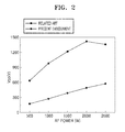
FIG. 2 is a graph comparing a plasma potential difference of the apparatus ofFIG. 1 with that of an existing apparatus; -
FIG. 3 is a cross-sectional side view of a portion of the display device manufactured by the apparatus ofFIG. 1 ; and -
FIG. 4 is a graph illustrating a water vapor transmission characteristic of an inorganic layer in the display device ofFIG. 3 . - Hereinafter, exemplary embodiments of the present invention are described, examples of which are illustrated in the accompanying drawings, wherein like reference numerals refer to like elements throughout. In this regard, the present exemplary embodiments may have different forms and should not be construed as being limited to the descriptions set forth herein. Accordingly, the exemplary embodiments are merely described below, by referring to the figures, to explain aspects of the present invention.
- It will be understood that although the terms "first", "second", etc. may be used herein to describe various components, these components should not be limited by these terms. These components are only used to distinguish one component from another.
- As used herein, the singular forms "a," "an" and "the" are intended to include the plural forms as well, unless the context clearly indicates otherwise.
- It will be further understood that the terms "comprises" and/or "comprising" used herein specify the presence of stated features or components, but do not preclude the presence or addition of one or more other features or components.
- It will be understood that when a layer, region, or component is referred to as being "formed on," another layer, region, or component, it can be directly or indirectly formed on the other layer, region, or component. That is, for example, intervening layers, regions, or components may be present.
- Sizes of elements in the drawings may be exaggerated for convenience of explanation. In other words, since sizes and thicknesses of components in the drawings are arbitrarily illustrated for convenience of explanation, the following embodiments are not limited thereto.
- When a certain embodiment may be implemented differently, a specific process order may be performed differently from the described order. For example, two consecutively described processes may be performed substantially at the same time or performed in an order opposite to the described order.
- As used herein, the term "and/or" includes any and all combinations of one or more of the associated listed items. Expressions such as "at least one of," when preceding a list of elements, modify the entire list of elements and do not modify the individual elements of the list.
- As used herein, the term "existing apparatus" refers to a standard apparatus for forming a display device as is typical in the prior art. Similarly, the term "existing process" refers to a standard process of manufacturing a display device as is typical in the prior art, i.e., a process according to an existing apparatus. The term "existing display device" similarly refers to a display device that is typical in the prior art, for example, a display device that is manufactured according to an existing process or an existing apparatus.
-
FIG. 1 is a schematic view of anapparatus 100 for manufacturing a display device according to one or more embodiments of the present invention.FIG. 2 is a graph comparing a plasma potential difference of theapparatus 100 ofFIG. 1 with that of an existing apparatus. - Referring to
FIGS. 1 and2 , theapparatus 100 may include achamber 111, ashower head 120, aplasma generation unit 131, apower supply unit 132, asusceptor 140, adriving unit 150, agas supply unit 161, acleaning unit 162, amask 171, amask fixing unit 172, avision unit 191, anexhaust unit 180, and a control unit. - The
chamber 111 may have a space therein and may include an opening 111a through which asubstrate 210 may be inserted or withdrawn. Agate valve 112 may be installed at the opening 111a such that thegate valve 112 opens or closes the opening 111a. - The
shower head 120 may be located inside thechamber 111. Theshower head 120 may include ashower head body 121 having a space therein and abaffle 122 located inside theshower head body 121. - The
shower head body 121 may have at least onespray hole 121a. Theshower head body 121 may be connected to thegas supply unit 161 that supplies a mixed gas to theshower head body 121. The mixed gas is then sprayed inside of thechamber 111 through the at least onespray hole 121a. - The
baffle 122 may partition the space inside theshower head body 121. Thebaffle 122 may supply the mixed gas supplied from thegas supply unit 161 to the at least onespray hole 121a at a uniform pressure. - The mixed gas may be formed in various ways. For example, the mixed gas may include a reaction gas and an inert gas. In one or more embodiments, the reaction gas may include a silicon precursor such as silane (SiH4) or the like, the reaction gas may include nitrogen (N2) or ammonia (NH3), and the inert gas may include a helium (He) gas or the like. The inert gas may be used as a purge gas or a carrier gas.
- The reaction gas and the inert gas may be supplied to the
shower head body 121 separately. As such, the reaction gas and the inert gas may be mixed inside theshower head body 121 and sprayed into thechamber 111. In other embodiments, the reaction gas and the inert gas may be sprayed from theshower head body 121 into thechamber 111 separately and mixed inside thechamber 111. However, for convenience of description, reference is made herein to embodiments wherein the reaction gas and the inert gas are mixed inside theshower head body 121 and sprayed into thechamber 111. - The
plasma generation unit 131 may be mounted inside thechamber 111 to generate plasma from the mixed gas. According to one or more embodiments, theplasma generation unit 131 may have an electrode form mounted on theshower head 120. Alternatively, in other embodiments, theplasma generation unit 131 may form a potential difference between the susceptor 140 and an outer wall of thechamber 111 or between theshower head 120 and thesusceptor 140. As such, theplasma generation unit 131 may have a cable form connected to each of thesusceptor 140 and thechamber 111 or connected to each of theshower head 120 and thesusceptor 140. - The
plasma generation unit 131 of embodiments of the invention is not limited thereto and may include any device and any structure capable of generating plasma from the mixed gas. However, for convenience of description, reference is made herein to embodiments wherein theplasma generation unit 131 has an electrode form mounted on theshower head 120. - The
power supply unit 132 may supply a current to theplasma generation unit 131. Thepower supply unit 132 may include a high-frequency power supply. A frequency of the current supplied from thepower supply unit 132 to theplasma generation unit 131 may be controlled (or maintained at a specified frequency). For example, the frequency of the current supplied from thepower supply unit 132 to theplasma generation unit 131 may be from about 27 MHz to about 42 MHz. - The
susceptor 140 may be formed such that asubstrate 210 is seated on thesusceptor 140. Thesusceptor 140 may include atemperature control unit 142 for controlling a temperature of thesubstrate 210. Thetemperature control unit 142 may include at least one of a cooling unit and a heater unit. - The
susceptor 140 may include alifter 141 for linearly moving thesubstrate 210. As such, thelifter 141 may adjust a gap between thesubstrate 210 and themask 171 by linearly moving the substrate 210 (i.e., moving thesubstrate 210 up or down). - The driving
unit 150 may be connected to thesusceptor 140 and may move thesusceptor 140 linearly. According to one or more embodiments, the drivingunit 150 may include a cylinder connected to thesusceptor 140. According to another embodiment, the drivingunit 150 may include a ball screw connected to thesusceptor 140 and a motor for rotating the ball screw. The drivingunit 150 of embodiments of the invention is not limited thereto and may include any device or any structure connected to thesusceptor 140 such that thesusceptor 140 may move linearly. However, for convenience of description, reference is made herein to embodiments wherein thedriving unit 150 includes a cylinder. - The
gas supply unit 161 may supply the reaction gas and the inert gas to theshower head 120. For example, thegas supply unit 161 may supply the reaction gas and the inert gas to theshower head 120 separately. Specifically, thegas supply unit 161 may supply at least one of the reaction gas and the inert gas according to a process of manufacturing the display device. - The
cleaning unit 162 may be connected to theshower head 120 to supply a cleaning gas. The cleaning gas may be an inert gas such as He or the like. Thecleaning unit 162 may include a remote plasma system (RPS) for generating plasma from the cleaning gas. As the RPS is the same as or similar to a general or typical RPS, a detailed description thereof is omitted. - The
mask 171 may be located between the susceptor 140 and theshower head 120. Themask 171 may have at least onepattern part 171a through which the mixed gas passes. The at least onepattern part 171a may specify a portion wherein the mixed gas is deposited. For example, when a plurality of display devices are manufactured, eachpattern part 171a may correspond to each display unit D. As another example, when one display device is manufactured, onepattern part 171a may correspond to a display unit D of thesubstrate 210. - The
mask 171 may be seated on themask fixing unit 172. Themask fixing unit 172 may be formed in a bracket form, a clamp form, or the like such that themask 171 is seated on themask fixing unit 172. In addition, themask fixing unit 172 may be formed to move in various directions. - The
vision unit 191 may be located outside thechamber 111. Thevision unit 191 may photograph themask 171 and thesubstrate 210. An image captured by thevision unit 191 may be transmitted to the control unit. - The
exhaust unit 180 may discharge gases inside thechamber 111 to the outside. Theexhaust unit 180 may include anexhaust pipe 181 connected to thechamber 111 and apump 182 mounted on theexhaust pipe 181. - The control unit may be electrically connected to the
power supply unit 132, thesusceptor 140, the drivingunit 150, thegas supply unit 161, thecleaning unit 162, themask fixing unit 172, thevision unit 191, and theexhaust unit 180 to be able to individually (or separately) control thepower supply unit 132, thesusceptor 140, the drivingunit 150, thegas supply unit 161, thecleaning unit 162, themask fixing unit 172, thevision unit 191, and theexhaust unit 180. - The control unit may be a PC, a laptop computer, a portable terminal, a cellular phone, or the like. In one or more embodiments, the control unit may be a circuit board or the like. However, the control unit of embodiments of the invention is not limited thereto and may have any form capable of controlling an operation of the
apparatus 100. - Hereinafter, a method of manufacturing a display device by using the
apparatus 100 is described. First, thesubstrate 210 on which the display unit D is formed may be supplied to the inside of thechamber 111 by a robot arm or the like. Theexhaust unit 180 may maintain atmospheric pressure inside thechamber 111. In addition, thegate valve 112 may open theopening 111a. Thelifter 141 may elevate upward to support thesubstrate 210. - After inserting and seating the
substrate 210, themask 171 may be inserted into thechamber 111 from the outside. Thereafter, themask 171 may be seated on themask fixing unit 172. - After inserting the
substrate 210 and themask 171 into thechamber 111, theexhaust unit 180 may maintain the pressure inside thechamber 111 to a low pressure similar to a vacuum. Then, thevision unit 191 may photograph locations of thesubstrate 210 and themask 171 and transmit the captured image to the control unit. Specifically, thevision unit 191 may photograph alignment marks respectively formed on thesubstrate 210 and themask 171 and transmit the captured image to the control unit. - The control unit may analyze the captured image to determine whether the
mask 171 and thesubstrate 210 are aligned. If it is determined that thesubstrate 210 and themask 171 are not aligned, the control unit may adjust the location of thesubstrate 210 or themask 171 by controlling thelifter 141 or themask fixing unit 172. - After completing the alignment, if it is determined that the locations of the
substrate 210 and themask 171 are aligned, the control unit may supply the reaction gas and the inert gas through thegas supply unit 161. In this case, the control unit may control thegas supply unit 161 to first spray the purge gas and then supply the reaction gas and the carrier gas, and may control theplasma generation unit 131 to generate plasma from the reaction gas and the carrier gas. - The plasma generated from the reaction gas and the carrier gas may be sprayed onto the
substrate 210 through theshower head 120. In this case, the control unit may control thepower supply unit 132 to adjust a frequency of a current to be applied to theplasma generation unit 131 so that the frequency is between about 27 MHz and about 42 MHz. In addition, thesusceptor 140 may maintain a temperature of thesubstrate 210 at about 100°C or less. In addition, a partial pressure ratio of silane in the mixed gas may be between about 30% and about 80%. If the partial pressure ratio of silane in the mixed gas is less than 30%, the generation of ionized reactive species of silane is too small, thereby decreasing a deposition speed, and if the partial pressure ratio of silane in the mixed gas exceeds 80%, the generation of ionized reactive species of silane is too large, thereby decreasing a deposition efficiency. - As described above, when a thin film is formed using the plasma while the temperature of the
substrate 210 is maintained at about 100°C or less, a portion of an organic material formed on the display unit D may be damaged due to a potential difference between charged particles because of the generation of the plasma. In addition, when the process described above is performed while maintaining the temperature of thesubstrate 210 at about 100°C or less, the dissolution of silane may be accelerated by using a hydrogen (H) gas to maximize the radical formation of silane. However, when the H gas is used, a side effect caused by the H gas may occur. - Therefore, according to one or more embodiments, the side effect may be prevented by performing the process while maintaining the temperature of the
substrate 210 at about 100°C or less and without using the H gas. - When the deposition is performed while the frequency of the current is maintained as described above, an inorganic layer may be formed on the display unit D. In this case, a deposition speed of the inorganic layer may be about 0.45 µm/min or more. The deposition speed according to one or more embodiments of the present invention is at least two times faster than the typical deposition speed according to an existing apparatus.
- When plasma density increases, collisions between particles may increase, thereby increasing the deposition speed. Herein, the plasma density may be proportional to a square of the frequency of the current. A current density between electrodes of the
plasma generation unit 131 may also be proportional to a square of the frequency of the current. - As such, when the frequency of the current increases, the plasma density and the current density may also increase. When the plasma density increases, the deposition speed increases, the current density increases, and a potential difference formed by the plasma decreases. Thus, damage to the display unit D caused by the plasma may be prevented (or minimized).
- In other words, when the temperature of the
substrate 210 is about 100°C or less as described above, the deposition speed is not influenced by the temperature of thesubstrate 210, and an impedance of the plasma may influence the deposition speed. In this case, the deposition speed may be inversely proportional to the impedance of the plasma, and thus, when the impedance of the plasma is minimized, the deposition speed may increase. Therefore, according to one or more embodiments, the impedance of the plasma may be minimized by decreasing the potential difference of the plasma to a half or less, and, by minimizing the impedance of the plasma, the deposition speed may increase two times or more relative to the deposition speed according to an existing apparatus. - Referring to
FIG. 2 , when power of theplasma generation unit 131 increases, the potential difference of the plasma decreases to about half of the potential difference as compared with the existing process. In addition, as compared with the existing process, an increasing speed of the potential difference of the plasma may be significantly slow along with the increase in the power of thepower supply unit 132. The power of thepower supply unit 132 may increase by changing the frequency of the current. Accordingly, the potential difference of the plasma may be formed low, and the current density may increase. Specifically, according to one or more embodiments, as compared with the existing process, a higher current density may be formed since the potential difference of the plasma is lower in a same power condition, and thus, more ionized active species may be formed and the deposition speed may increase by two times or more. - As shown in Table 1, below, the inorganic layer manufactured by using the
apparatus 100 and the method of manufacturing a display device according to one or more embodiments of the present invention may be formed more densely than an inorganic layer manufactured by using an existing apparatus and an existing method. - According to one or more embodiments, without using H, a bond ratio of Si-H may decrease from the existing value of about 33-35% to about 25.71%. In addition, according to one or more embodiments, by generating more ionized active species (as compared to the ionized active species generated by the existing apparatus) by dissolving a silane gas, a bond ratio of Si-nitrogen (N) may increase from the typical value of about 55-53% to about 62.28%. In this case, the existing process uses a plasma chemical vapor deposition (CVD) method using about 13.56 MHz, and the present embodiment uses about 27 MHz.
- As discussed, the mixed gas may include ammonia or nitrogen in addition to silane (SiH4). It will be appreciated that SiH4 is dissolved into SiH2 or SiH3 during a process, a SiHx dangling bond is coupled to a thin film surface, NH3 is dissolved into or NH, thereby forming a Si and Si-N bond on the thin film surface, an H radical reacts to H of NHx, thereby forming H2, a dangling bond of H may perform a Si and Si-N bond, and a N-H bond may be mostly generated by NH3.
Table 1 Bonding Bond ratio (%) Existing process Present embodiment Si-N 55.53 62.28 Si-H 33.35 25.71 N-H 11.12 12.01 - The bond ratios of Si-N, Si-O, Si-H, and N-H may be checked by measuring an absorbance rate of each bond through an FT-IR (Fourier Transform Infrared Spectroscopy) method.
- Specifically, the inorganic layer may have a water vapor transmission ratio (WVTR) of about 5x10⁻⁵ g/m2day or less. Thus, the WVTR of the inorganic layer may decrease about ten times or more relative to the WVTR, of an inorganic layer formed according to an existing process.
- After forming the inorganic layer through the process described above, an organic layer may be formed on the inorganic layer. Then an inorganic layer may be formed on the organic layer, and an organic layer may also be formed on the inorganic layer. In other words, the inorganic layer and the organic layer may be alternately and repeatedly stacked to form alternating layers.
- Therefore, the
apparatus 100 and the method of manufacturing a display device may deposit the inorganic layer at a faster speed (e.g., at least two times faster) at a low temperature as compared with the existing apparatus and the existing method. In addition, theapparatus 100 and the method of manufacturing a display device may protect the display unit D below the inorganic layer from external moisture, thus improving the life span of the display device -
FIG. 3 is a cross-sectional side view of a portion of adisplay device 200 manufactured by theapparatus 100 ofFIG. 1 .FIG. 4 is a graph showing a water vapor transmission characteristic of an inorganic layer in thedisplay device 200 ofFIG. 3 . - Referring to
FIGS. 3 and4 , thedisplay device 200 may include thesubstrate 210 and a display unit. In addition, thedisplay device 200 may include a thin-film encapsulation layer E or an encapsulation substrate formed on the display unit. The encapsulation substrate is the same as or similar to that used for a general display device, and thus a detailed description thereof is omitted. For convenience of description, reference is made herein to embodiments wherein thedisplay device 200 includes the thin-film encapsulation layer E. - The display unit may be formed on the
substrate 210. The display unit may include a thin-film transistor TFT, apassivation layer 270 and an organic light emitting diode (OLED) 280. Thepassivation layer 270 may be formed to cover the thin-film transistor TFT, and theOLED 280 may be formed on thepassivation layer 270. - The
substrate 210 may include a glass material. However, thesubstrate 210 of embodiments of the invention is not necessarily limited thereto and may include a plastic material or a metallic material such as steel use stainless (SUS) or titanium (Ti). Alternatively, thesubstrate 210 may include polyimide (PI). For convenience of description, reference is made herein to embodiments wherein thesubstrate 210 includes a glass material. - A
buffer layer 220 formed of an organic compound and/or an inorganic compound is formed on an upper surface of thesubstrate 210. Thebuffer layer 220 may be formed of silicon oxide (SiOx) (x≥1) or silicon nitride (SiNx) (x≥1). - An
active layer 230 arranged in a predetermined pattern is formed on thebuffer layer 220 and is buried (or covered) by agate insulating layer 240. Theactive layer 230 includes asource region 231 and adrain region 233 and further includes achannel region 232 therebetween. - The
active layer 230 may be formed to include various materials. For example, theactive layer 230 may include an inorganic semiconductor material such as amorphous silicon or crystalline silicon. As another example, theactive layer 230 may include an oxide semiconductor. As another example, theactive layer 230 may include an organic semiconductor material. However, for convenience of description reference is made herein to embodiments wherein theactive layer 230 includes amorphous silicon. - The
active layer 230 may be formed by forming an amorphous silicon layer on thebuffer layer 220, crystallizing the amorphous silicon layer to form a polycrystalline silicon layer, and patterning the polycrystalline silicon layer. Thesource region 231 and thedrain region 233 of theactive layer 230 are doped with impurities according to a thin-film transistor type, such as a driving thin-film transistor, a switching thin-film transistor, or the like. - A
gate electrode 250 facing theactive layer 230 and an interlayer insulatinglayer 260 which buries thegate electrode 250 are formed on an upper surface of thegate insulating layer 240. - Contact holes H1 are formed in the
interlayer insulating layer 260 and thegate insulating layer 240, and asource electrode 271 and adrain electrode 272 are formed on theinterlayer insulating layer 260 such that thesource electrode 271 and thedrain electrode 272 contact thesource region 231 and thedrain region 233, respectively. - The
passivation layer 270 is formed on the thin-film transistor TFT formed as described above, and apixel electrode 281 of theOLED 280 is formed on thepassivation layer 270. Thepixel electrode 281 contacts thedrain electrode 272 of the thin-film transistor TFT through a via hole H2 formed in thepassivation layer 270. Thepassivation layer 270 may be formed of an inorganic material and/or an organic material and in a single layer or two or more layers, wherein thepassivation layer 270 may be formed as a planarization layer such that an upper surface thereof is planarized regardless of the unevenness of a lower layer or formed uneven along the unevenness of the lower layer. Thepassivation layer 270 may be formed of a transparent insulator so that a resonance effect is achieved. - After forming the
pixel electrode 281 on thepassivation layer 270, a pixel-defininglayer 290 is formed of an organic material and/or an inorganic material such that the pixel-defininglayer 290 covers at least a portion of thepixel electrode 281 and thepassivation layer 270 but exposes at least a portion of thepixel electrode 281 therethrough. - An
intermediate layer 282 and anopposite electrode 283 are formed on at least thepixel electrode 281. - In one or more embodiments, the
pixel electrode 281 may function as an anode, and theopposite electrode 283 may function as a cathode. In one or more embodiments, thepixel electrode 281 may function as a cathode and theopposite electrode 283 may function as an anode. - The
pixel electrode 281 and theopposite electrode 283 are insulated from each other by theintermediate layer 282, and when voltages of different polarities are applied to theintermediate layer 282, an organic emission layer emits light. - The
intermediate layer 282 may include the organic emission layer. Alternatively, theintermediate layer 282 may include the organic emission layer and may further include at least one selected from the group consisting of a hole injection layer (HIL), a hole transport layer (HTL), an electron transport layer (ETL), and an electron injection layer (EIL). - One unit pixel includes a plurality of sub-pixels R, G and B, and the plurality of sub-pixels R, G and B may emit light of various colors. For example, the unit pixel may include the plurality of sub-pixels R, G and B that respectively emit red light, green light, and blue light, or a plurality of sub-pixels that respectively emit red light, green light, blue light, and white light.
- The thin-film encapsulation layer E may include a plurality of inorganic layers or may include an inorganic layer and an organic layer. The organic layer of the thin-film encapsulation layer E is formed of a polymer and may be a single-layer film or a multi-layer film formed of polyethylene terephthalate (PET), PI, polycarbonate (PC), epoxy, polyethylene, or polyacrylate. Further, the organic layer may be formed of polyacrylate, and in detail, the organic layer may include a polymerized monomer composition including a diacrylate-based monomer and a triacrylate-based monomer. The monomer composition may further include a monoacrylate-based monomer. The monomer composition may further include a well-known photoinitiator, such as TPO, but embodiments of the invention are not limited thereto.
- The inorganic layer of the thin-film encapsulation layer E may be a single-layer film or a multi-layer film including a metal oxide or a metal nitride. For example, the inorganic layer may include SiNx, Al2O3, SiO2, or TiO2.
- The uppermost layer exposed to the outside in the thin-film encapsulation layer E may be formed of an inorganic layer to prevent infiltration of moisture to the
OLED 280. - The thin-film encapsulation layer E may include at least one sandwich structure in which at least one organic layer is interposed between at least two inorganic layers. As another example, the thin-film encapsulation layer E may include at least one sandwich structure in which at least one inorganic layer is interposed between at least two organic layers. As another example, the thin-film encapsulation layer E may include a sandwich structure in which at least one organic layer is interposed between at least two inorganic layers and a sandwich structure in which at least one inorganic layer is interposed between at least two organic layers.
- The thin-film encapsulation layer E may sequentially include a first inorganic layer U1, a first organic layer O1, and a second inorganic layer U2 from an upper part of the
OLED 280. - As another example, the thin-film encapsulation layer E may sequentially include the first inorganic layer U1, the first organic layer O1, the second inorganic layer U2, a second organic layer, and a third inorganic layer from the upper part of the
OLED 280. - As another example, the thin-film encapsulation layer E may sequentially include the first inorganic layer U1, the first organic layer O1, the second inorganic layer U2, the second organic layer, the third inorganic layer, a third organic layer, and a fourth inorganic layer from the upper part of the
OLED 280. - A halogenated metal layer including lithium fluoride (LiF) may be further included between the
OLED 280 and the first inorganic layer. The halogenated metal layer may prevent theOLED 280 from being damaged when the first inorganic layer is formed by a sputtering method. - The first organic layer may have a smaller area than the second inorganic layer, and the second organic layer may also have a smaller area than the third inorganic layer.
- For convenience of description, reference is made herein to embodiments wherein the thin-film encapsulation layer E includes the first inorganic layer U1, the first organic layer O1, and the second inorganic layer U2.
- The first inorganic layer U1 and the second inorganic layer U2 may be manufactured by the
apparatus 100 and the method of manufacturing a display device, which have been described with reference toFIGS. 1 and2 . Since the first inorganic layer U1 and the second inorganic layer U2 are the same or similar to each other, the first inorganic layer U1 is described below for convenience of description. - The first inorganic layer U1 formed as described above may have a WVTR of 5x1-5 g/m2day or less as described above. Therefore, the
display device 200 has a lower WVTR, than the existing display device, and thus, the display unit D may be effectively protected from external moisture. - The first inorganic layer U1 may have a refractive index of between about 1.8 and about 1.88. In addition, the first inorganic layer U1 may have an inorganic layer transmission rate of about 90% or more at 450 nm. Therefore, as compared to an existing display device, the
display device 200 has a substantially similar transmission rate and refractive index, and thus, thedisplay device 200 may realize the same image quality as the existing display device. - The first inorganic layer U1 may have a stress of about -200 MPa to about 200 MPa. Therefore, the
display device 200 has a similar stress as compared to an existing display device, and thus, thedisplay device 200 may realize the same strength as the existing display device. - In addition, the first inorganic layer U1 may have a bond ratio of Si-N which is about 60% or more and a bond ratio of Si-H which is about 30% or less. Since the bond ratio of Si-N is about 60% or more, the first inorganic layer U1 may be formed more densely than the inorganic layer of the existing display device. Therefore, the
display device 200 may have an improved WVTR, as compared to the existing display device. - As discussed, embodiments of the invention can provide a display device comprising: a substrate; a display unit on the substrate; and an inorganic layer on the display unit, wherein a water vapor transmission rate, WVTR, of the inorganic layer is 5x10⁻⁵ g/m2day or less.
- In some embodiments, the inorganic layer includes a metal oxide or a metal nitride, optionally wherein the inorganic layer comprises SiNx, Al2O3, SiO2, or TiO2. In some embodiments, the inorganic layer may comprise SiNH. In some embodiments, a bond ratio of silicon (Si)-nitride (N) in the inorganic layer is about 60% or greater, and a bond ratio of Si-hydrogen (H) is about 30% or less.
In some embodiments, the inorganic layer forms part of an encapsulation layer arranged to cover the display unit. The encapsulation layer may comprise a structure in which at least one organic layer is interposed between at least two inorganic layers (one or more of which having a WVTR, of 5x10⁻⁵ g/m2day or less); or a structure in which at least one said inorganic layer is interposed between at least two organic layers. The encapsulation layer may comprise various combinations of inorganic layers and organic layers. - Embodiments of the invention can also provide an apparatus for manufacturing a display device, the apparatus comprising: a chamber; a shower head for spraying a mixed gas into the chamber; a plasma generation unit for forming plasma from the mixed gas; a susceptor facing the shower head and on which a substrate is seated; and a power supply unit electrically connected to the plasma generation unit, wherein a frequency of a current supplied from the power supply unit to the plasma generation unit is from about 27 MHz to about 42 MHz. The mixed gas may include a reaction gas and an inert gas, and the reaction gas may include silane.
- As described above, an apparatus and method for manufacturing a display device having an inorganic layer for minimizing the infiltration of moisture may be formed according to one or more of the above exemplary embodiments.
- It should be understood that the exemplary embodiments described herein should be considered in a descriptive sense only and not for purposes of limitation. Descriptions of features or aspects within each exemplary embodiment should typically be considered as available for other similar features or aspects in other exemplary embodiments.
- While one or more exemplary embodiments have been described with reference to the figures, it will be understood by those of ordinary skill in the art that various changes in form and details may be made therein without departing from the scope of the invention as defined by the following claims.
Claims (15)
- A display device comprising:a substrate;a display unit on the substrate; andan inorganic layer on the display unit,wherein a water vapor transmission rate, WVTR, of the inorganic layer is 5x1-5 g/m2day or less.
- The display device of claim 1, wherein a refractive index of the inorganic layer is between about 1.8 and about 1.88.
- The display device of claim 1 or 2, wherein a transmission rate of the inorganic layer at 450 nm is about 90% or greater.
- The display device of any one of claims 1 to 3, wherein a stress of the inorganic layer is between about -200 MPa and about 200 MPa.
- The display device of any one of claims 1 to 4, wherein the inorganic layer includes a metal oxide or a metal nitride, optionally wherein the inorganic layer comprises SiNx, Al2O3, SiO2, or TiO2.
- The display device of claim 5, wherein a bond ratio of silicon (Si)-nitride (N) in the inorganic layer is about 60% or greater, and a bond ratio of Si-hydrogen (H) is about 30% or less.
- The display device of any one of claims 1 to 6, wherein the inorganic layer forms part of an encapsulation layer arranged to cover the display unit.
- The display device of claim 7, wherein the encapsulation layer comprises a structure in which at least one organic layer is interposed between at least two said inorganic layers; or
wherein the encapsulation layer comprises a structure in which at least one said inorganic layer is interposed between at least two organic layers. - The display device of any one of claims 1 to 8, wherein the inorganic layer forms an outermost layer over the display unit.
- An apparatus for manufacturing a display device, the apparatus comprising:a chamber;a shower head for spraying a mixed gas into the chamber;a plasma generation unit for forming plasma from the mixed gas;a susceptor facing the shower head and on which a substrate is seated; anda power supply unit electrically connected to the plasma generation unit,wherein a frequency of a current supplied from the power supply unit to the plasma generation unit is from about 27 MHz to about 42 MHz.
- The apparatus of claim 10, wherein a temperature of the substrate is maintained at about 100°C or less.
- The apparatus of claim 10 or 11, wherein a partial pressure ratio of silane in the mixed gas is from about 30% to about 80%.
- A method of manufacturing a display device, the method comprising:forming a display unit on a substrate;seating and aligning the substrate on a susceptor inside a chamber; andforming an inorganic layer on the display unit by spraying a plasma mixed gas onto the display unit through a shower head,wherein the shower head includes a plasma generation unit for forming plasma from the mixed gas, and a frequency of a current of power supplied to the plasma generation unit is from about 27 MHz to about 42 MHz.
- The method of claim 13, wherein a water vapor transmission rate, WVTR, of the inorganic layer is 5x1-5 g/m2day or less.
- The display device of claim 13 or 14, wherein the inorganic layer includes a metal oxide or a metal nitride, optionally wherein the inorganic layer comprises SiNx, Al2O3, SiO2, or TiO2.
Applications Claiming Priority (1)
| Application Number | Priority Date | Filing Date | Title |
|---|---|---|---|
| KR1020140156236A KR102393372B1 (en) | 2014-11-11 | 2014-11-11 | Display device, method for manufacturing a display device |
Publications (1)
| Publication Number | Publication Date |
|---|---|
| EP3021375A1 true EP3021375A1 (en) | 2016-05-18 |
Family
ID=54539904
Family Applications (1)
| Application Number | Title | Priority Date | Filing Date |
|---|---|---|---|
| EP15193834.7A Withdrawn EP3021375A1 (en) | 2014-11-11 | 2015-11-10 | Display device and apparatus and method for manufacturing the same |
Country Status (4)
| Country | Link |
|---|---|
| US (2) | US9722206B2 (en) |
| EP (1) | EP3021375A1 (en) |
| KR (1) | KR102393372B1 (en) |
| CN (1) | CN105590952B (en) |
Families Citing this family (2)
| Publication number | Priority date | Publication date | Assignee | Title |
|---|---|---|---|---|
| CN206685388U (en) * | 2017-03-14 | 2017-11-28 | 京东方科技集团股份有限公司 | A kind of encapsulating structure, display panel and display device |
| KR20240123479A (en) * | 2023-02-06 | 2024-08-14 | 삼성디스플레이 주식회사 | Display panel and method of the manufacturing of the same |
Citations (7)
| Publication number | Priority date | Publication date | Assignee | Title |
|---|---|---|---|---|
| US20070184181A1 (en) * | 2003-03-25 | 2007-08-09 | Kazuo Wada | Device and method for forming film for organic electro-luminescence element using inductive coupling CVD |
| US20090051272A1 (en) * | 2005-02-17 | 2009-02-26 | Konica Minolta Holdings, Inc. | Gas barrier film, gas barrier film manufacturing method, resin substrate for organic electroluminescent device using the aforesaid gas barrier film, and organic electroluminescent device using the aforementioned gas barrier film |
| US20090197101A1 (en) * | 2008-02-01 | 2009-08-06 | Fujifilm Corporation | Gas barrier layer deposition method, gas barrier film and organic el device |
| WO2009099009A1 (en) * | 2008-02-08 | 2009-08-13 | Fuji Electric Holdings Co., Ltd. | Organic el display and manufacturing method of the same |
| US20090218943A1 (en) * | 2008-03-03 | 2009-09-03 | Sony Corporation | Display device and electronic equipment |
| US20100187986A1 (en) * | 2007-07-31 | 2010-07-29 | Sumitomo Chemical Company, Limited | Organic electroluminescence device and method for producing the same |
| US20110121271A1 (en) * | 2009-11-25 | 2011-05-26 | Hee-Song Jeon | Organic light emitting diode display |
Family Cites Families (18)
| Publication number | Priority date | Publication date | Assignee | Title |
|---|---|---|---|---|
| JPS5730325A (en) * | 1980-07-30 | 1982-02-18 | Nec Corp | Manufacture of amorphous silicon thin film |
| JPH09129627A (en) | 1995-10-27 | 1997-05-16 | Hitachi Electron Eng Co Ltd | Plasma CVD apparatus and semiconductor manufacturing method |
| JP3918496B2 (en) * | 2001-10-22 | 2007-05-23 | 株式会社日立製作所 | Liquid crystal display device and manufacturing method thereof |
| JP2003239071A (en) | 2002-02-14 | 2003-08-27 | Mitsubishi Heavy Ind Ltd | Method and apparatus for film deposition by plasma cvd |
| US20030203210A1 (en) | 2002-04-30 | 2003-10-30 | Vitex Systems, Inc. | Barrier coatings and methods of making same |
| US7086918B2 (en) | 2002-12-11 | 2006-08-08 | Applied Materials, Inc. | Low temperature process for passivation applications |
| US7510913B2 (en) | 2003-04-11 | 2009-03-31 | Vitex Systems, Inc. | Method of making an encapsulated plasma sensitive device |
| US7300829B2 (en) | 2003-06-02 | 2007-11-27 | Applied Materials, Inc. | Low temperature process for TFT fabrication |
| JP4408713B2 (en) | 2004-02-03 | 2010-02-03 | Necエレクトロニクス株式会社 | Manufacturing method of semiconductor device |
| KR101171192B1 (en) * | 2005-10-21 | 2012-08-06 | 삼성전자주식회사 | Tft substrate and making method of the same |
| KR20070102764A (en) | 2006-04-17 | 2007-10-22 | 주식회사 엘지화학 | Method for manufacturing multilayer thin film structure based on PCC method |
| KR20100022404A (en) * | 2008-08-19 | 2010-03-02 | 삼성에스디아이 주식회사 | Filter for plasma display panel and plasma display apparatus having the same |
| KR100997110B1 (en) | 2009-01-23 | 2010-11-30 | 엘지전자 주식회사 | Process for Preparation of Thin Layered Structure |
| JP5394867B2 (en) * | 2009-09-17 | 2014-01-22 | 富士フイルム株式会社 | Gas barrier film and gas barrier film |
| US9884341B2 (en) * | 2011-08-12 | 2018-02-06 | Massachusetts Institute Of Technology | Methods of coating surfaces using initiated plasma-enhanced chemical vapor deposition |
| WO2014119750A1 (en) * | 2013-01-31 | 2014-08-07 | コニカミノルタ株式会社 | Gas barrier film |
| CN105246683A (en) * | 2013-05-28 | 2016-01-13 | 柯尼卡美能达株式会社 | Gas-barrier film and process for producing the same |
| KR102266448B1 (en) * | 2014-07-29 | 2021-06-16 | 엘지디스플레이 주식회사 | Organic light emitting diode display and manufacturing method of the same |
-
2014
- 2014-11-11 KR KR1020140156236A patent/KR102393372B1/en active Active
-
2015
- 2015-07-28 US US14/811,729 patent/US9722206B2/en active Active
- 2015-11-10 EP EP15193834.7A patent/EP3021375A1/en not_active Withdrawn
- 2015-11-11 CN CN201510764886.1A patent/CN105590952B/en active Active
-
2017
- 2017-07-03 US US15/640,945 patent/US10211427B2/en active Active
Patent Citations (7)
| Publication number | Priority date | Publication date | Assignee | Title |
|---|---|---|---|---|
| US20070184181A1 (en) * | 2003-03-25 | 2007-08-09 | Kazuo Wada | Device and method for forming film for organic electro-luminescence element using inductive coupling CVD |
| US20090051272A1 (en) * | 2005-02-17 | 2009-02-26 | Konica Minolta Holdings, Inc. | Gas barrier film, gas barrier film manufacturing method, resin substrate for organic electroluminescent device using the aforesaid gas barrier film, and organic electroluminescent device using the aforementioned gas barrier film |
| US20100187986A1 (en) * | 2007-07-31 | 2010-07-29 | Sumitomo Chemical Company, Limited | Organic electroluminescence device and method for producing the same |
| US20090197101A1 (en) * | 2008-02-01 | 2009-08-06 | Fujifilm Corporation | Gas barrier layer deposition method, gas barrier film and organic el device |
| WO2009099009A1 (en) * | 2008-02-08 | 2009-08-13 | Fuji Electric Holdings Co., Ltd. | Organic el display and manufacturing method of the same |
| US20090218943A1 (en) * | 2008-03-03 | 2009-09-03 | Sony Corporation | Display device and electronic equipment |
| US20110121271A1 (en) * | 2009-11-25 | 2011-05-26 | Hee-Song Jeon | Organic light emitting diode display |
Also Published As
| Publication number | Publication date |
|---|---|
| US20160133873A1 (en) | 2016-05-12 |
| US9722206B2 (en) | 2017-08-01 |
| CN105590952B (en) | 2021-09-28 |
| KR20160056465A (en) | 2016-05-20 |
| CN105590952A (en) | 2016-05-18 |
| US10211427B2 (en) | 2019-02-19 |
| KR102393372B1 (en) | 2022-05-03 |
| US20170309864A1 (en) | 2017-10-26 |
Similar Documents
| Publication | Publication Date | Title |
|---|---|---|
| KR101990555B1 (en) | Thin film encapsulation manufacturing device and manufacturing method of thin film encapsulation | |
| US7220687B2 (en) | Method to improve water-barrier performance by changing film surface morphology | |
| CN104115300B (en) | Methods of Depositing Encapsulation Films | |
| US10202683B2 (en) | Thin film encapsulation layer manufacturing apparatus and method of manufacturing display apparatus using the same | |
| KR101673016B1 (en) | Thin film encapsulation manufacturing device and manufacturing method of display apparatus using the same | |
| KR20150125667A (en) | Fluorine-containing plasma polymerized hmdso for oled thin film encapsulation | |
| US10590533B2 (en) | Method of manufacturing display apparatus utilizing mask assembly including intermediate layer and self-assembled monolayer | |
| CN110010799B (en) | Device and method for manufacturing display device | |
| WO2014163773A1 (en) | Plasma curing of pecvd hmdso film for oled applications | |
| US10041173B2 (en) | Apparatus and method of manufacturing display apparatus | |
| KR20120107331A (en) | Method for fabricating organic light emitting display device and the organic light emitting display device fabricated by the method | |
| TW200535262A (en) | Method and apparatus of depositing low temperature inorganic films on plastic substrates | |
| KR102405123B1 (en) | Apparatus for manufacturing display apparatus and method of manufacturing display apparatus | |
| US10211427B2 (en) | Display device and apparatus and method for manufacturing the same | |
| TWI693736B (en) | Display apparatus and method of manufacturing display apparatus | |
| US9803279B2 (en) | Apparatus and method for manufacturing display apparatus | |
| KR102832574B1 (en) | Organic light emitting display and method for manufacturing the same |
Legal Events
| Date | Code | Title | Description |
|---|---|---|---|
| PUAI | Public reference made under article 153(3) epc to a published international application that has entered the european phase |
Free format text: ORIGINAL CODE: 0009012 |
|
| AK | Designated contracting states |
Kind code of ref document: A1 Designated state(s): AL AT BE BG CH CY CZ DE DK EE ES FI FR GB GR HR HU IE IS IT LI LT LU LV MC MK MT NL NO PL PT RO RS SE SI SK SM TR |
|
| AX | Request for extension of the european patent |
Extension state: BA ME |
|
| STAA | Information on the status of an ep patent application or granted ep patent |
Free format text: STATUS: REQUEST FOR EXAMINATION WAS MADE |
|
| 17P | Request for examination filed |
Effective date: 20161118 |
|
| RBV | Designated contracting states (corrected) |
Designated state(s): AL AT BE BG CH CY CZ DE DK EE ES FI FR GB GR HR HU IE IS IT LI LT LU LV MC MK MT NL NO PL PT RO RS SE SI SK SM TR |
|
| STAA | Information on the status of an ep patent application or granted ep patent |
Free format text: STATUS: EXAMINATION IS IN PROGRESS |
|
| 17Q | First examination report despatched |
Effective date: 20180620 |
|
| STAA | Information on the status of an ep patent application or granted ep patent |
Free format text: STATUS: THE APPLICATION IS DEEMED TO BE WITHDRAWN |
|
| 18D | Application deemed to be withdrawn |
Effective date: 20200207 |