EP3021200A1 - Electrode for touch sensor, touch panel, and display device - Google Patents
Electrode for touch sensor, touch panel, and display device Download PDFInfo
- Publication number
- EP3021200A1 EP3021200A1 EP14822992.5A EP14822992A EP3021200A1 EP 3021200 A1 EP3021200 A1 EP 3021200A1 EP 14822992 A EP14822992 A EP 14822992A EP 3021200 A1 EP3021200 A1 EP 3021200A1
- Authority
- EP
- European Patent Office
- Prior art keywords
- electrode
- electrodes
- strip
- sensing
- drive
- Prior art date
- Legal status (The legal status is an assumption and is not a legal conclusion. Google has not performed a legal analysis and makes no representation as to the accuracy of the status listed.)
- Granted
Links
Images




Classifications
-
- G—PHYSICS
- G06—COMPUTING OR CALCULATING; COUNTING
- G06F—ELECTRIC DIGITAL DATA PROCESSING
- G06F3/00—Input arrangements for transferring data to be processed into a form capable of being handled by the computer; Output arrangements for transferring data from processing unit to output unit, e.g. interface arrangements
- G06F3/01—Input arrangements or combined input and output arrangements for interaction between user and computer
- G06F3/03—Arrangements for converting the position or the displacement of a member into a coded form
- G06F3/041—Digitisers, e.g. for touch screens or touch pads, characterised by the transducing means
- G06F3/044—Digitisers, e.g. for touch screens or touch pads, characterised by the transducing means by capacitive means
- G06F3/0446—Digitisers, e.g. for touch screens or touch pads, characterised by the transducing means by capacitive means using a grid-like structure of electrodes in at least two directions, e.g. using row and column electrodes
-
- G—PHYSICS
- G06—COMPUTING OR CALCULATING; COUNTING
- G06F—ELECTRIC DIGITAL DATA PROCESSING
- G06F1/00—Details not covered by groups G06F3/00 - G06F13/00 and G06F21/00
- G06F1/16—Constructional details or arrangements
-
- G—PHYSICS
- G06—COMPUTING OR CALCULATING; COUNTING
- G06F—ELECTRIC DIGITAL DATA PROCESSING
- G06F3/00—Input arrangements for transferring data to be processed into a form capable of being handled by the computer; Output arrangements for transferring data from processing unit to output unit, e.g. interface arrangements
- G06F3/01—Input arrangements or combined input and output arrangements for interaction between user and computer
- G06F3/03—Arrangements for converting the position or the displacement of a member into a coded form
- G06F3/041—Digitisers, e.g. for touch screens or touch pads, characterised by the transducing means
- G06F3/0412—Digitisers structurally integrated in a display
-
- G—PHYSICS
- G06—COMPUTING OR CALCULATING; COUNTING
- G06F—ELECTRIC DIGITAL DATA PROCESSING
- G06F3/00—Input arrangements for transferring data to be processed into a form capable of being handled by the computer; Output arrangements for transferring data from processing unit to output unit, e.g. interface arrangements
- G06F3/01—Input arrangements or combined input and output arrangements for interaction between user and computer
- G06F3/03—Arrangements for converting the position or the displacement of a member into a coded form
- G06F3/041—Digitisers, e.g. for touch screens or touch pads, characterised by the transducing means
- G06F3/044—Digitisers, e.g. for touch screens or touch pads, characterised by the transducing means by capacitive means
- G06F3/0445—Digitisers, e.g. for touch screens or touch pads, characterised by the transducing means by capacitive means using two or more layers of sensing electrodes, e.g. using two layers of electrodes separated by a dielectric layer
-
- G—PHYSICS
- G06—COMPUTING OR CALCULATING; COUNTING
- G06F—ELECTRIC DIGITAL DATA PROCESSING
- G06F3/00—Input arrangements for transferring data to be processed into a form capable of being handled by the computer; Output arrangements for transferring data from processing unit to output unit, e.g. interface arrangements
- G06F3/01—Input arrangements or combined input and output arrangements for interaction between user and computer
- G06F3/03—Arrangements for converting the position or the displacement of a member into a coded form
- G06F3/041—Digitisers, e.g. for touch screens or touch pads, characterised by the transducing means
- G06F3/044—Digitisers, e.g. for touch screens or touch pads, characterised by the transducing means by capacitive means
- G06F3/0448—Details of the electrode shape, e.g. for enhancing the detection of touches, for generating specific electric field shapes, for enhancing display quality
-
- H—ELECTRICITY
- H05—ELECTRIC TECHNIQUES NOT OTHERWISE PROVIDED FOR
- H05K—PRINTED CIRCUITS; CASINGS OR CONSTRUCTIONAL DETAILS OF ELECTRIC APPARATUS; MANUFACTURE OF ASSEMBLAGES OF ELECTRICAL COMPONENTS
- H05K1/00—Printed circuits
- H05K1/02—Details
- H05K1/0296—Conductive pattern lay-out details not covered by sub groups H05K1/02 - H05K1/0295
-
- G—PHYSICS
- G06—COMPUTING OR CALCULATING; COUNTING
- G06F—ELECTRIC DIGITAL DATA PROCESSING
- G06F2203/00—Indexing scheme relating to G06F3/00 - G06F3/048
- G06F2203/041—Indexing scheme relating to G06F3/041 - G06F3/045
- G06F2203/04111—Cross over in capacitive digitiser, i.e. details of structures for connecting electrodes of the sensing pattern where the connections cross each other, e.g. bridge structures comprising an insulating layer, or vias through substrate
-
- G—PHYSICS
- G06—COMPUTING OR CALCULATING; COUNTING
- G06F—ELECTRIC DIGITAL DATA PROCESSING
- G06F2203/00—Indexing scheme relating to G06F3/00 - G06F3/048
- G06F2203/041—Indexing scheme relating to G06F3/041 - G06F3/045
- G06F2203/04112—Electrode mesh in capacitive digitiser: electrode for touch sensing is formed of a mesh of very fine, normally metallic, interconnected lines that are almost invisible to see. This provides a quite large but transparent electrode surface, without need for ITO or similar transparent conductive material
Definitions
- This disclosure related to electrodes for a touch sensor having a plurality of electrodes arranged along one direction, a touch panel having the electrodes for a touch sensor, and a display unit.
- a touch sensor provided in a display unit has a drive electrode and a sensing electrode, which are examples of electrodes for a touch sensor, and detects contact of a finger or the like on an operation surface as a change in an electrical capacitance between the drive electrode and the sensing electrode. Images which a display panel forms are output to the operation surface through the drive electrode and the sensing electrode. Accordingly, the drive electrode and the sensing electrode are formed as , for example, aggregates of many electrode wires arranged with spaces between each other (for example, see PTL1).
- the electrical capacitance between the drive electrode and the sensing electrode is measured by a peripheral circuit connected to the electrodes for the touch sensor.
- the initial value of the electrical capacitance between the electrodes needs to be appropriate value with respect to the amount of change in electrical capacitance due to the contact. This demand is satisfied generally by forming each of the plurality of electrodes into a shape and size equal to each other and arranging keeping certain spaces therebetween.
- a portion selected by the finger, on the operation surface is defined within the output range of images on the operation surface.
- the output image includes a portion which cannot be selected by the finger.
- the area where the drive electrodes are arranged or the area where the sensing electrodes are arranged is too much larger than the image output area, measurement of the electrical capacitances between the electrodes is wastefully repeated. Accordingly, the size of the area where the electrodes are arranged needs to be the same as the output range of images. This demand is satisfied generally by matching the size of the area where the electrodes are arranged to the size of the display panel.
- a size of a unit area needed for arranging one electrode is defined on the basis of a standard for improving detection accuracy of the electrical capacitance.
- the size of the area where the drive electrodes are arranged or the size of the area where the sensing electrodes are arranged is determined on the basis of the size of another device other than the touch sensor.
- the size of the other device other than the touch sensor is ordinarily different from a whole-number multiple of the above unit area of the electrode.
- the edge of the output image does not include any electrode portion essentially needed for detecting the contact.
- the end of the area where the electrodes are arranged includes an electrode portion which is essentially not needed as a target area of sensing.
- the size of the area needed for arranging one electrode is defined, if the drive electrodes and the sensing electrodes are arranged to cover the whole output image, a part of the electrodes is out of the image output area.
- the touch sensor In order to prevent the touch sensor from including the unnecessary part of the electrodes, if the unnecessary part of the electrodes, which is outside the output image, is omitted, resultingly the initial value of the electrical capacitance between the electrodes at the ends of the area where the electrodes are arranged becomes lower than that in other areas.
- the art of this disclosure has as its object the provision of electrodes for a touch sensor preventing the electrical capacitance at the end of an area where the electrodes are arranged from being lowered, and also a touch panel and a display unit.
- An aspect of electrodes for a touch sensor in this disclosure has a plurality of strip electrodes arranged along an arrangement direction which is one direction, with spaces therebetween, wherein each of the strip electrodes is an aggregate of a plurality of electrode wires disposed with spaces therebetween, the plurality of strip electrodes are equal in total area of the plurality of electrode wires of each strip electrode, the plurality of strip electrodes include an end strip electrode and another strip electrode other than the end strip electrode, the end strip electrode being located at least at one end in the arrangement direction, and when a ratio of a total area of the electrode wires to an area of a respective strip electrode is defined as an area ratio in the strip electrode, the area ratio in the end strip electrode is different from the area ratio in the other strip electrode.
- An aspect of a touch panel in this disclosure has the above-described electrodes for a touch sensor, and a cover layer covering the electrodes for a touch sensor, wherein the electrodes for a touch sensor have a transparent substrate, a plurality of first strip electrodes arranged on a surface of the transparent dielectric substrate along a first direction, keeping spaces therebetween, and a plurality of second strip electrodes arranged on a back surface of the transparent dielectric substrate along a second direction, keeping spaces therebetween, at least one of the first strip electrode and the second strip electrode is the strip electrode, and the touch panel further has a peripheral circuit measuring electrical capacitances between the first strip electrodes and the second strip electrodes.
- An aspect of a display unit in this disclosure has a display panel displaying information, a drive circuit driving the display panel, the touch panel transmitting therethrough the information which the display panel displays.
- the end strip electrode disposed at least at one end in the arrangement direction is equal to the other strip electrode in total area of the electrode wires of each strip electrode, and differs in area ratio of the total area of the electrode wires to the area of the strip electrode from the other strip electrode. Therefore, in the end strip electrode, while the area of the strip electrode itself is different from that of the other strip electrode, the electrical capacitance is prevented from being smaller than the electrical capacitance of the other strip electrode.
- a touch panel and a display unit are embodied.
- a configuration of the display unit is described with reference to Fig. 1 .
- the display unit is a laminate where a display panel 10, such as a liquid crystal panel or an organic EL panel which is driven by a drive circuit, and a touch panel 20 are stuck together with a transparent adhesive layer.
- a display surface 10S formed as a rectangle is laid out on a surface of the display panel 10, and the display surface 10S displays thereon images on the basis of external image data.
- the touch panel is a laminate where an electrode 21 for a touch sensor and a cover layer 22 are stuck together with a transparent adhesive layer 23.
- the cover layer 22 is made from such as a glass substrate or a resin film.
- a surface of the cover layer 22 opposite to the transparent adhesive layer 23 serves as an operation surface 20S of the touch panel 20.
- the transparent adhesive layer 23 has optical transparency which allows image displayed on the display surface 10S to pass therethrough.
- a polyether-based adhesive agent or an acrylic-based adhesive agent is used for the transparent adhesive layer 23.
- the electrodes 21 for a touch sensor and the cover layer 22 may be stuck together with the transparent adhesive layer 23, or, as another method different from this, the following method may be adopted. That is, a thin film layer made of a conductive metal, such as copper, is formed directly or through an under layer on the cover layer 22 such as of a resin film. On top of that, there is formed a resist layer having pattern shape of the electrodes for a touch sensor. Subsequently, using a wet etching method using such as ferric chloride, the thin film layer is formed to be the electrode for a touch sensor extending along an X direction, thereby obtaining a first film.
- a thin film layer made of a conductive metal such as copper
- the thin film is formed to be the electrodes for a touch sensor extending along a Y direction, thereby obtaining a second film. Thereafter, the first film and the second film are stuck together with the transparent adhesive layer 23.
- a transparent substrate 31 which is a constituent element of the electrode 21 for a touch sensor and an example of a first substrate, is layered on the whole display surface 10S formed in the display panel 10, and allows images formed on the display surface 10S to pass therethrough.
- the transparent substrate 31 is made of, for example, a substrate such as of transparent glass substrate or transparent resin film.
- the transparent substrate 31 may have a single-layer structure made of one substrate, or may have a multi-layer structure where two or more substrates are layered.
- a surface of the transparent substrate 31 opposite to the display panel 10 is designed to be the drive surface 31S.
- a plurality of drive electrode wires 31L which are only an example of electrode wires, are arranged along a first arrangement direction D1, which is one direction.
- Each of the drive electrode wires 31L is formed into a zigzag line extending along a second arrangement direction D2 perpendicular to the first arrangement direction D1.
- Each of the drive electrode wires 31L is grouped by nine in order from the drive electrode wire 31L at the end of the first arrangement direction D1.
- Nine drive electrode wires 31L included in one group are connected to one pad 31T, and the nine drive electrode wires 31L arranged at intervals along the first arrangement direction D1 configure one drive electrode 31DP, an example of a first strip electrode.
- a metal film made of such as copper or aluminum, a metal oxide film made of such as zinc oxide, or a complex oxide film made of such as indium tin oxide or indium gallium zinc oxide is used for each of the drive electrode wires 31L.
- Indium tin oxide or indium gallium zinc oxide is formed from a metal oxide including indium, tin, gallium, zinc and the like.
- a silver nanowire, a conductive polymer film or a conductive film is also used for each of the drive electrode wires 31L.
- the conductive films include a graphene film or the like.
- the drive electrodes 31DP each including nine drive electrode wires 31L are connected to a selection circuit 34 respectively, and receive drive voltage applied by the selection circuit 34 to be selected.
- the drive electrode wires 31L and the pads 31T may be formed at the same time by etching a thin film formed on the drive surface 31S through a mask.
- the drive electrode wires 31L and the pads 31T may be made of materials different from each other by the respective processes.
- the drive electrode wires 31L and the pads 31T may be formed on the respective substrates different from the transparent substrate 31, and formed by pasting the drive electrode wires 31L and the pads 31T from the respective substrates onto the transparent substrate 31.
- the drive surface 31S, the drive electrode wires 31L and the pads 31T are pasted together on a transparent dielectric substrate 33, which is an example of a second substrate, with a transparent adhesive layer 32.
- the transparent adhesive layer 32 has optical transparency to allow images displayed on the display surface 10S to pass through.
- the transparent adhesive layer 32 binds the combination of the drive surface 31S, the drive electrode wires 31L and the pads 31T to the transparent dielectric substrate 33.
- a polyether-based adhesive agent or an acrylic-based adhesive agent is used for the transparent adhesive layer 32.
- the transparent adhesive layer 32 and the transparent dielectric substrate 33 are constituent elements.
- the drive electrode wires 31L and the pads 31T are formed on the back surface of the transparent dielectric substrate.
- the transparent dielectric substrate 33 is, for example, made of a substrate such as a transparent resin film of polyethylene terephthalate or a transparent glass substrate.
- the transparent dielectric substrate 33 may have a single-layer structure formed by one substrate, or may have a multiple-layer structure where two or more substrates are layered.
- the transparent dielectric substrate 33 has optical transparency for allowing the image displayed on the display surface 10S to pass therethrough and appropriate relative permittivity to detect electrical capacitance between electrodes.
- the surface of the transparent dielectric substrate 33 opposite to the transparent adhesive layer 32 is set to be a sensing surface 33S.
- a plurality of sensing electrode wires 33L are arranged along the second arrangement direction D2.
- Each of the sensing electrode wires 33L is formed into a zigzag line extending along the first arrangement direction D1.
- Each of the sensing electrode wires 33L is assigned to a respective group of nine in order from the sensing electrode wire 33L at the end of the second arrangement direction D2.
- Nine sensing electrode wires 33L included in one group are connected to one pad 33T.
- the nine sensing electrode wires 33L connected to the one pad 33T and arranged at intervals along the second arrangement direction D2 configure one sensing electrode 33SP, an example of the facing strip electrode which is a second strip electrode.
- a metal film made of such as copper or aluminum, a metal oxide film made of such as zinc oxide, or a complex oxide film made of such as indium tin oxide or indium gallium zinc oxide is used for each of the sensing electrode wires 33L.
- Indium tin oxide or indium gallium zinc oxide is formed from a metal oxide including indium, tin, gallium, zinc and the like.
- a silver nanowire, a conductive polymer film or a conductive film is also used for each of the sensing electrode wires 33L.
- the conductive films include a graphene film or the like.
- the sensing electrodes 33SP each including nine sensing electrode wires 33L are connected to a detection circuit 35 respectively. The voltages of the respective sensing electrodes 33SP are detected by the detection circuit 35.
- the sensing electrode wires 33L and the pads 33T may be formed at the same time by etching a thin film formed on the sensing surface 33S through a mask.
- the sensing electrode wires 33L and the pads 33T may be made of materials different from each other by respective processes.
- the sensing electrode wires 33L and the pads 33T may be formed on respective substrates different from the transparent dielectric substrate 33, and formed by pasting the sensing electrode wires 33L and the pads 33T from the respective substrates onto the transparent dielectric substrate 33.
- the sensing surface 33S, the sensing electrode wires 33L and the pads 33T are pasted together on a cover layer 22 with the transparent adhesive layer 23 described above.
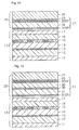
- Fig. 2 shows a cross-section structure of the display unit. It should be noted that Fig. 2 shows a liquid crystal panel as an example of the display panel.
- the transparent substrate 31, the drive electrodes 31 DP, the transparent adhesive layer 32, the transparent dielectric substrate 33, the sensing electrodes 33SP, the transparent adhesive layer 23 and the cover layer 22 are disposed.
- the transparent adhesive layer 32 is disposed between the drive electrode 31DP and the transparent dielectric substrate 33, covering the peripheral of each electrode wire 31L configuring the drive electrode 31DP and filling spaces between the adjacent electrode wires 31L.
- the transparent adhesive layer 23 is disposed between the sensing electrode 33SP and the cover layer 22, covering the periphery of each electrode wire 33L configuring the sensing electrode 33SP and filling spaces between the adjacent electrode wires 33L.
- a plurality of constituent elements of the display panel 10 are arranged as follows. That is, in order from the constituent element furthest from the touch panel 20, a lower polarizer 11, a thin film transistor (referred to as a TFT) substrate 12, a TFT layer 13, a liquid crystal layer 14, a color filter layer 15, a color filter substrate 16 and an upper polarizer 17 are disposed. Of these, at the TFT layer 13, pixel electrodes configuring sub pixels are disposed in a matrix. In the color filter layer 15, black matrices define a plurality of areas each having a rectangular shape facing each of the sub pixels. In each of the areas defined by the black matrices, there is disposed the color layer which changes white light to light of any one of red, green or blue color.
- the touch panel 20 has the selection circuit 34, the detection circuit 35, and a control section 36.
- the selection circuit 34 can be connected to the drive electrodes 31DP.
- the detection circuit 35 can be connected to the sensing electrodes 33SP.
- the control section 36 is connected to the selection circuit 34 and the detection circuit 35.
- the control section 36 generates a start timing signal for making the selection circuit 34 start generating a drive signal to each of the drive electrodes 31DP, and outputs it.
- the control section 36 generates a scan timing signal for making the selection circuit 34 scan targets to which the drive signal is supplied serially from a first drive electrode 31DP1 to an n-th drive electrode 31DPn, and outputs it.
- the control section 36 generates a start timing signal for making the detection circuit 35 start detecting the current passing through each sensing electrode 33SP, and outputs it.
- the control section 36 generates a scan timing signal for making the detection circuit 35 scan targets to be detected serially from a first sensing electrode 33SP1 to the n-th sensing electrode 33SPn, and output it.
- the selection circuit 34 starts generating the drive signal on the basis of the start timing signal which the control section 36 has output, and scans output targets of the drive signal from the first drive electrode 31DP1 to the n-th drive electrode 31DPn on the basis of the scan timing signal which the control section 36 has output.
- the detection circuit 35 has a signal acquiring section 35a and a signal processing section 35b.
- the signal acquiring section 35a starts acquiring a current signal which is an analog signal generated in each sensing electrode 33SP, on the basis of the start timing signal which the control section 36 has output. Thereafter, the signal acquiring section 35a scans acquisition targets of the current signal from a first sensing electrode 33SP1 to n-th sensing electrode 33SPn, on the basis of the scan timing signal which the control section 36has output.
- the signal processing section 35b processes each current signal which the signal acquiring section 35a has acquired, generates a voltage signal which is a digital value, and outputs the generated voltage signal to the control section 36.
- the selection circuit 34 and the detection circuit 35 generate a voltage signal from a current signal which changes depending on change in electrical capacitance, thereby measuring change in electrical capacitance between the drive electrode 31DP and the sensing electrode 33SP.
- the selection circuit 34 and the detection circuit 35 are an example of a peripheral circuit driving the electrodes for the touch panel.
- the control section 36 detects the position on the touch panel 20 which a user is contacting, on the basis of the voltage signal which the signal processing section 35b has output.
- the touch panel 20 is not limited to the aforementioned mutual-capacitance type touch panel 20, but may be a self-capacitance type touch panel.
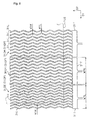
- Fig. 4 is a plan view showing the planar structure of the drive electrode 31DP.
- Fig. 5 is a plan view of the drive electrode 31DP and the sensing electrode 33SP viewed from a direction in which the drive electrode 31DP and the sensing electrode 33SP are layered. It should be noted that the line widths of the drive electrode wire 31L and the line widths of the sensing electrode wire 33L are emphasized in Fig. 4 and Fig. 5 , for convenience of description of the arrangement of the drive electrode wires 31L and arrangement of the sensing electrode wires 33L.
- one drive electrode 31DP includes the nine drive electrode wires 31L formed in a zigzag shape extending along the second arrangement direction D2, and is the strip electrode extending along the second arrangement direction D2. That is, each area of the drive electrodes 31DP includes, in the drive surface 31S, the nine drive electrode wires 31L and the spaces between the drive electrode wires 31L adjacent to each other. The drive electrodes 31DP are equal to each other in area of each drive electrode. Each of the drive electrodes 31DP are arranged along the first direction D1.
- the drive electrodes 31DP disposed at both ends in the area where the drive electrodes 31DP are arranged are set as end drive electrodes 31DE.
- the drive electrodes 31DP other than the end drive electrodes 31DE are set as middle drive electrodes 31DM.
- each position of the middle drive electrodes 31DM is a position overlapping the display surface 10S.
- the length along the first direction D1 of the middle drive electrodes 31DM are set as middle electrode widths WPM, and the middle electrode width WPM is set at, for example, 5.4 mm.
- each position of the two end drive electrodes 31DE is a position extending outside of the display surface 10S from within the display surface 10S.
- the length along the first arrangement direction D1 is set as an end electrode width WPE.
- the end electrode width WPE is smaller than that of the middle electrode width WPM, and is set at, for example, 4.8 mm.
- the end electrode width WPE is smaller than the middle electrode width WPM. Therefore, in the area where the drive electrodes 31DP having the end electrode widths WPE and the middle electrode width WPM are arranged, the length along the first arrangement direction D1 is smaller compared to the configuration where all drive electrodes 31DP have the middle electrode width WPM. This prevents the end portion of the area where the drive electrodes are arranged from including any area other than the target area of sensing.
- the target area of sensing is the portion overlapping the display surface 10S, of the area where the drive electrodes 31DP are arranged.
- each drive electrode wire 31L the length along the first arrangement direction D1 is set as a drive electrode wire width W1L, and the drive electrode wire width W1L is set at, for example, 5 ⁇ m.
- the spaces between the drive electrode wires 31L adjacent to each other are set as drive electrode wire space widths W1W.
- the drive electrode wire space width W1W is set at, for example, 600 ⁇ m.
- the drive electrode wire 31L of the end drive electrode 31DE has the same width as the drive electrode wire 31L of the middle drive electrode 31DM. That is, each total area occupied by nine drive electrode wires 31L of each drive electrode 31DP in each of the plurality of the drive electrodes 31DP is even in the drive surface 31S and equal to each other.
- the width of the drive electrode wire 31L of the end drive electrode 31DE may be larger than the width of the drive electrode wire 31L of the middle drive electrode 31DM.
- the spaces between the drive electrode wires 31L adjacent to each other are set as drive electrode wire space widths W1W and end drive electrode wire space widths W1N.
- the end drive electrode wire space width W1N is set at, for example, 300 ⁇ m, 1/2 of the drive electrode wire space width W1W.
- the end drive electrode 31DE includes portions having the drive electrode wire space widths W1W as an example of the first electrode portion, and includes portions having the end drive electrode wire space widths W1N as an example of the second electrode portion.
- the end drive electrode wire space width W1N is smaller than the drive electrode wire space width W1W. Accordingly, the area occupied by the drive electrode wires 31L in the unit area of the end drive electrode 31DE is larger than the area occupied by the drive electrode wires 31L in the unit area of the middle drive electrode 31DM. In other words, in the end drive electrode 31DE, the ratio of the total area of the drive electrode wires 31L to the area of the drive electrode 31DP is larger than the ratio in the middle drive electrode 31DM.
- the unit area of the drive electrode 31DP is a size including two or more drive electrode wire 31L in the middle drive electrode 31DM.
- two drive electrode wires 31L separated from each other by the end drive electrode wire space width W1N are disposed at the ends of the area in which the drive electrodes 31DP are arranged.
- the drive electrode wires 31L arranged with the end drive electrode wire space width W1N therebetween are disposed more densely than the drive electrode wires 31L arranged with the drive electrode wire space width W1W therebetween.
- the drive electrode wires 31L arranged with the end drive electrode wire space width W1N therebetween are disposed at the ends of the area where the drive electrodes 31DP are arranged, the drive electrode wires 31L arranged densely are difficult to view.
- the end drive electrode wire space width W1N is twice the thickness of the transparent dielectric substrate 33 or more. If the end drive electrode wire space width W1N is twice the thickness of the transparent dielectric substrate 33 or more, variation in density of the drive electrode wires 31L becomes difficult to see. As the end drive electrode wire space width W1N become small, the electrical capacitance between the drive electrode wires 31L becomes large. In this regard, if the end drive electrode wire space width W1N is twice the thickness of the transparent dielectric substrate 33 or more, variation in electrical capacitance between the drive electrode wire 31L and the sensing electrode wire 33L due to the electrical capacitance between the drive electrode wires 31L can be suppressed.
- one sensing electrode 33SP includes the nine sensing electrode wires 33L formed in a zigzag shape extending along the first arrangement direction D1, and is the strip electrode extending along the first arrangement direction D1. That is, each area of the sensing electrodes 33SP includes, in the sensing surface 33S, the nine sensing electrode wires 33L and the spaces between the sensing electrode wires 33L adjacent to each other. The sensing electrodes 33SP are equal to each other in area of each sensing electrode. Each of the sensing electrodes 33SP is arranged along the second direction D2, and is disposed at a position where it crosses a respective drive electrode 31DP when viewed from the direction of the planar view.
- the sensing electrodes 33SP disposed at both ends in the area where the sensing electrodes 33SP are arranged are set as end sensing electrodes 33SE.
- the sensing electrodes 33SP other than the end sensing electrodes 33SE are set as middle sensing electrodes 33SM.
- each position of the middle sensing electrodes 33SM is a position overlapping the display surface 10S.
- the length along the second direction D2 of the middle sensing electrodes 33SM are set as middle electrode widths WSM, and the middle electrode width WSM is set at, for example, 5.4 mm.
- each position of the two end sensing electrodes 33SE is a position extending outside of the display surface 10S from within the display surface 10S.
- the length along the second arrangement direction D2 is set as an end electrode width WSE.
- the end electrode width WSE is smaller than that of the middle electrode width WSM, and is set at, for example, 4.8 mm like the end electrode width WPE.
- the end electrode width WSE is smaller than the middle electrode width WSM. Therefore, in the area where the sensing electrodes 33SP having the end electrode widths WSE and the middle electrode width WSM are arranged, the length along the second arrangement direction D2 is smaller, compared to the configuration where all sensing electrodes 33SP have the middle electrode width WSM. This prevents the end portion of the area where the sensing electrodes are arranged from including any area other than the target area of sensing.
- each sensing electrode wire 33L the length along the second arrangement direction D2 is set as a sensing electrode wire width W3L, and the sensing electrode wire width W3L is set at, for example, 5 ⁇ m.
- the sensing electrode wires 33L of the middle drive electrode 33SM the spaces between the sensing electrode wires 33L adjacent to each other are set as sensing electrode wire space widths W3W.
- the sensing electrode wire space width W3W is set at, for example, 600 ⁇ m.
- the sensing electrode wire 33L of the end sensing electrode 33SE has the same width as the sensing electrode wire 33L of the middle sensing electrode 33SM. That is, each total area occupied by nine sensing electrode wires 33L of each sensing electrode 33SP in each of the sensing electrodes 33SP is uniform in the sensing surface 33S and equal to each other.
- the width of the sensing electrode wire 33L of the end sensing electrode 33SE may be larger than the width of the sensing electrode wire 33L of the middle sensing electrode 33SM.
- the spaces between the sensing electrode wires 33L adjacent to each other are set as sensing electrode wire space widths W3W and end sensing electrode wire space widths W3N.
- the end sensing electrode wire space width W3N is set at, for example, 300 ⁇ m, 1/2 of the sensing electrode wire space width W3W.
- the end sensing electrode 33SE includes portions having the sensing electrode wire space widths W3W as an example of the first electrode portion, and includes portions having the end sensing electrode wire space widths W3N as an example of the second electrode portion.
- the end sensing electrode wire space width W3N is smaller than the sensing electrode wire space width W3W. Accordingly, the area occupied by the sensing electrode wires 33L in the unit area of the end sensing electrode 33SE is larger than the area occupied by the sensing electrode wires 33L in the unit area of the middle sensing electrode 33SM. In other words, in the end sensing electrode 33SE, the ratio of the total area of the sensing electrode wires 33L to the area of the sensing electrode 33SP is larger than the ratio in the middle sensing electrode 33SM.
- the unit area of the sensing electrode 33SP is a size including two or more sensing electrode wires 33L in the middle sensing electrode 33SM.
- sensing electrode wires 33L separated from each other by the end sensing electrode wire space width W3N are disposed at the ends of the area where the sensing electrodes 33SP are arranged.
- the sensing electrode wires 33L arranged with the end sensing electrode wire space width W3N therebetween are disposed more densely than the sensing electrode wires 33L arranged with the sensing electrode wire space width W3W therebetween.
- the sensing electrode wires 33L arranged with the end sensing electrode wire space width W3N therebetween are disposed at the ends of the area where the sensing electrodes 33SP are arranged, the sensing electrode wires 33L arranged densely are difficult to see.
- the end sensing electrode wire space width W3N has twice the thickness of the transparent dielectric substrate 33 or more. If the end sensing electrode wire space width W3N has twice the thickness of the transparent dielectric substrate 33 or more, variation in density of the sensing electrode wires 33L becomes difficult to see. As the end sensing electrode wire space width W3N becomes small, the electrical capacitance between the sensing electrode wires 33L becomes large. In this regard, if the end sensing electrode wire space width W3N has twice the thickness of the transparent dielectric substrate 33 or more, variation in electrical capacitance between the sensing electrode wire 31L and the sensing electrode wire 33L due to the electrical capacitance between the sensing electrode wires 33L can be suppressed.
- each thickness of constituent members, relative permittivity and sheet resistance are set at the following values. Further, air layers which are 1 mm in thickness and 1.00 in relative permittivity are set on the upper side of the cover layer 22 and the lower side of the transparent substrate 31.
- the electrical capacitance between the drive electrode 31DP and the sensing electrode 33SP is calculated using a numerical calculation where the Laplace equation for a rectangular target area is solved by a finite element method. The rectangular target area ranges 5 mm along the first arrangement direction D1 and 5 mm along the second arrangement direction D2.
- the electrical capacitance between the drive electrode 31DP and the sensing electrode 33SP is 1.01 pF.
- the electrical capacitance between the middle sensing electrode 33SM and the middle drive electrode 31DM lowers to 0.79 pF.
- the configurations for making the end electrode width WPE smaller than the middle electrode width WPM there might be considered a configuration for reducing the number of the drive electrode wires 31L included in the end drive electrode 31DE.
- the configurations for making the end electrode width WSE smaller than the middle electrode width WSM there might be considered a configuration for reducing the number of the sensing electrode wires 33L included in the end sensing electrode 33SE.
- the electrical capacitance in the end drive electrode 31DE and the end sensing electrode 33SE is lower than the electrical capacitances in the other electrodes 31DP and 33SP.
- the area occupied by the electrode wires 31L, 33L in the unit area of the electrodes 31DP, 33SP having the end electrode widths WPE and WSE is larger than the area occupied by the electrode wires 31L, 33L in the unit area of the other electrodes 31DP, 33SP. Accordingly, as shown in the above results of the numerical calculation, the electrodes 31DP, 33SP having the end electrode widths WPE and WSE can have an electrical capacitance similar to those of the other electrodes 31DP, 33SP.
- the voltage width at a portion where the drive electrode 31DP and the sensing electrode 33SP intersect with each other in planar view is set at 1.0.
- a zone of not less than 0.8 and not more than 1.0 times the voltage width is set as a first voltage zone Z1, and a zone of not less than 0.7 and less than 0.8 times the voltage width is set as a second voltage zone Z2.
- a zone showing not less than 0.2 and less than 0.7 times the voltage width is set as a third voltage zone Z3.
- each thickness of composition members, relative permittivity and sheet resistance are set. Further, air layers which are 1 mm in thickness and 1.00 in relative permittivity are set on the upper side of the cover layer 22 and the lower side of the transparent substrate 31. Thereafter, the voltage applied to the sensing electrode 33SP is 0 V, the voltage applied to the drive electrode 31DP is changed from 3V to 20 V, a numerical calculation where the Laplace equation is solved by a finite element method is used, thereby calculating the voltage distribution between the drive electrode 31DP and the sensing electrode 33SP.
- the first voltage zone Z1, the second voltage zone Z2 and the third voltage zone Z3 intervene in the space between the sensing electrode wires 33L which are adjacent to each other. Accordingly, if the interval between the sensing electrode wires 33L adjacent to each other is the sensing electrode wire space width W3W, then between the sensing electrode wire 33L, the interference between the sensing electrode wires 33L can be regarded as negligible.
- the second voltage zone Z2 and the third voltage zone Z3 intervene in the space between the sensing electrode wires 33L adjacent to each other. Accordingly, if the space between the sensing electrode wires 33L adjacent to each other is the end sensing electrode wire space width W3N, thenbetween the sensing electrode wire 33L, the interference between the sensing electrode wires 33L is negligible.
- the space (300 ⁇ m) between the sensing electrode wires 33L adjacent to each other is at least twice or more the space between the drive electrode 31DP and the sensing electrode 33SP (150 ⁇ m), the interference between the sensing electrode wires 33L is negligible.
- the display panel 10 displays an image on the display surface 10S
- the image displayed on the display surface 10S is output to the surface of the cover layer 22 through the drive electrode 31DP and the sensing electrode 33SP.
- the area overlapping the display surface 10S in planar view is a portion that can be selected by a finger.
- the portion overlapping the display surface 10S is set as a target area of sensing.
- the drive electrodes 31DP are arranged in the whole target area of sensing.
- the portion overlapping the display surface 10S is set as a target area of sensing.
- the sensing electrodes 33SP are arranged in the whole target area of sensing. Accordingly, when a finger or the like contacts the output area of the image on the operation surface, the electrical capacitance between the drive electrode 31DP and the sensing electrode 33SP changes at the portion which the finger or the like contacts. The change in electrical capacitance is detected, thereby sensing the position at which the finger contacts on the operation surface.
- the length along the first arrangement direction D1 is shorter.
- the end electrode width WSE is smaller than the middle electrode width WSM, in the area where the sensing electrodes 33SP having the end electrode widths WSE and the middle electrode width WSM are arranged, the length along the second arrangement direction D2 is shorter. This prevents the end of the area where the drive electrodes 31DP are arranged and the end of the area where the sensing electrodes 33SP are arranged from including any portion other than the target area of sensing.
- the end drive electrode wire space width W1N is smaller than the drive electrode space width W1W
- the area occupied by the drive electrode wires 31L in the unit area of the end drive electrode 31DE is larger than the area occupied by the drive electrode wires 31L in the unit area of the middle drive electrode 31DM.
- the end sensing electrode wire space width W3N is smaller than the sensing electrode space width W3W
- the area occupied by the sensing electrode wires 33L in the unit area of the end sensing electrode 33SE is larger than the area occupied by the sensing electrode wires 33L in the unit area of the middle sensing electrode 33SM.
- the space between the end drive electrode wires 31L adjacent to each other is the drive electrode wire space width W1N.
- the space between the sensing electrode wire 33L adjacent to each other is the end sensing electrode wire space width W3N.
- the electrical capacitance between the wires (drive electrode wire 31L, sensing electrode wire 33L) in the end strip electrode (end drive electrode 31DE, end sensing electrode 33SE) is prevented from being larger than an electrical capacitance through the transparent dielectric substrate. Accordingly, detection accuracy of the electrical capacitance in the end strip electrode is further prevented from being lower than detection accuracy of the electrical capacitance in the other strip electrodes.
- the spaces between the adjacent sensing electrode wires 33L are set at the end sensing electrode wire space width W3N smaller than the sensing electrode wire space width W3W.
- the width of the drive electrode wire 31L in the end drive electrode 31DE may be the same as the width of the drive electrode wire 31L in the middle drive electrode 31DM.
- the end drive electrode wire space width W1N only has to be smaller than the drive electrode wire space width W1W.
- the end drive electrode wire space width W1N is set similar to the drive electrode wire space width W1W, and the above-described drive electrode wire 31L is set as the first drive electrode wire.
- the end drive electrode 31DE includes a smaller number of the first drive electrode wires than the middle drive electrode 31DM includes, the end drive electrode may include the second drive electrode wire 35L, which is an example of the second electrode wire, in addition to the first drive electrode wire, which is an example of the first electrode wire.
- the second drive electrode wire 35L is formed along a direction crossing the first drive electrode wire and the end drive electrode 31DE includes drive electrode wires formed into a grid-like shape.
- This configuration can also make the area occupied by the drive electrode wires in the unit area of the end drive electrode 31DE larger than the area occupied by the drive electrode wires in the unit area of the middle drive electrode 31DM. Since the space between the first drive electrode wires adjacent to each other is kept on the drive surface 31S, distribution of the density of the first drive electrode wires is prevented from being seen.
- the unit area is a size including two or more first drive electrode wires and one or more second drive electrode wires.
- the end drive electrode wire space width W1N may be smaller than the drive electrode wire space width W1W.
- the end sensing electrode wire space width W3N may be set similar to the sensing electrode wire space width W3W, and the above-described sensing electrode wire 33L may be set as the first drive electrode wire. While the end sensing electrode 33SE includes a smaller number of the first drive electrode wires than the middle sensing electrode 33SM includes, the end sensing electrode may include the second sensing electrode wire, which is an example of the second electrode wire, in addition to the first sensing electrode wire, which is an example of the first electrode wire. This configuration can also obtain, in the end sensing electrode 33SE, advantages similar to the above-described configuration of the end drive electrode 31DE.
- the end drive electrode 31DE of the above-described embodiment may further include the above-described second drive electrode wire, also the end sensing electrode 33SE of the above-described embodiment may further include the above-described second sensing electrode wire.
- the spaces between the drive electrode wires 31L adjacent to each other may be set at the end drive electrode wire space width W1N smaller than the drive electrode wire space width W1W, and the end drive electrode 31DE may include the above-described second drive electrode wire.
- the whole end sensing electrode 33SE, the spaces between the sensing electrode wires 33L adjacent to each other may be set at the end sensing electrode wire space width W3N smaller than the sensing electrode wire space width W3W, and the end sensing electrode 33SE may include the above-described second sensing electrode wire.
- the end drive electrode 31DE may include a drive electrode wire having a larger wire width than the drive electrode wire width W1L in the middle drive electrode 31DM. Even in this configuration, if the end electrode width WPE is smaller than the middle electrode width WPM and the area occupied by the drive electrode wires in the unit area of the end drive electrode 31DE is larger than that in the middle drive electrode 31DM, effects as above can be obtained. In this case, the unit area is a size including two or more drive electrode wires 31L.
- the end sensing electrode 33SE may include a sensing electrode wire having a larger wire width than the sensing electrode wire width W3L in the middle sensing electrode 33SM. Even in this configuration, if the end electrode width WSE is smaller than the middle electrode width WSM and the area occupied by the sensing electrode wires in the unit area of the end sensing electrode 33SE is larger than that in the middle sensing electrode 33SM, effects as above can be obtained. In this case, the unit area is a size including two or more sensing electrode wires 33L.
- the drive electrode wire spaces width W1W which is a distance between the drive electrode wires 31L adjacent to each other may be different between each pair of the drive electrode wires 31L adjacent to each other.
- the area occupied by the drive electrode wires 31L in the unit area of the end drive electrode 31DE only has to be larger than the area occupied by the drive electrode wires 31L in the unit area of the middle drive electrode 31DM.
- the sensing electrode wire spaces width W3W which is a distance between the snsing electrode wires 33L adjacent to each other may be different between each pair of the sensing electrode wires 33L adjacent to each other.
- the area occupied by the sensing electrode wires 33L in the unit area of the end sensing electrode 33SE only has to be larger than the area occupied by of the sensing electrode wires 33L in the unit area of the middle sensing electrode 33SM.
- the target area of sensing may be set at a portion other than the portion overlapping the display surface 10S, of the area where the drive electrodes 31DP are arranged. Also, the target area of sensing may be set at a portion other than the portion overlapping the display surface 10S, of the area where the sensing electrodes 33SP are arranged. For example, the target area of sensing may be an area specifically determined according to a demand from manufacturing processes or a structure of at least one of an electrode 21 for a touch sensor, a touch panel 20 and a display panel 10.
- only the drive electrode 31DP at one end in the first arrangement direction D1 may be set as the end drive electrode 31DE.
- the sensing electrode 33SP only the sensing electrode 33SP at one end in the first arrangement direction D1 may be set as the end sensing electrode 33SE.
- the end drive electrode wire space width W1N in the end drive electrode 31DE may be the same as the drive electrode wire space width W1W.
- the end sensing electrode wire space width W3N in the end sensing electrode 33SE may be the same as the sensing electrode wire space width W3W.
- the configuration only has to satisfy that the end drive electrode wire space width W1N is smaller than the drive electrode wire space width W1W or the end sensing electrode wire space width W3N is smaller than the sensing electrode wire space width W3W.
- each of the drive electrodes 31DP may be formed into a grid-like shape where the drive electrode wires cross each other.
- the end drive electrode 31DE only has to have a configuration where the density of the drive electrode wires is higher than the density in the middle drive electrode 31DM.
- the configuration only has to satisfy that the end electrode width WPE is smaller than the middle electrode width WPM and the area occupied by the drive electrodes in the unit area of the end drive electrode 31DE is larger than the area occupied by the drive electrodes in the unit area of the middle drive electrode 31DM.
- each of the sensing electrodes 33SP may be formed into a grid-like shape where the sensing electrode wires cross each other.
- the end sensing electrode 33SE only has to have a configuration where the density of the sensing electrode wires is higher than the density in the middle sensing electrode 33SM.
- the configuration only has to satisfy that the end electrode width WSE is smaller than the middle electrode width WSM and the area occupied by the sensing electrodes in the unit area of the end sensing electrode 33SE is larger than the area occupied by the sensing electrodes in the unit area of the middle sensing electrode 33SM.
- the end electrode width WPE may be larger than the middle electrode width WPM, also the end electrode width WSE may be larger than the middle electrode width WSM.
- the area occupied by the electrode wires in the unit area of the strip electrode (end strip electrode) disposed at the end of the arrangement direction only has to be larger than the area occupied by the electrode wires in the unit area of the other strip electrode.
- the drive electrode 31 DP may be a facing strip electrode (the second strip electrode), and the sensing electrode 33SP may be a strip electrode (the first strip electrode).
- the first substrate may support the plurality of the strip electrodes
- the second substrate may support the plurality of the facing strip electrodes
- the transparent dielectric substrate may include the first substrate and the second substrate. This configuration can increase freedom degree of capacitance which the transparent dielectric substrate has, since the capacitance which the transparent dielectric substrate has is determined by the capacitance of the first substrate and the capacitance of the second substrate.
- the first substrate may support the plurality of the strip electrodes
- the second substrate may support the plurality of the facing strip electrode
- the transparent dielectric substrate may be any one of the first substrate and the second substrate.
- the transparent dielectric substrate may be formed by one substrate.
- the second embodiment differs from the first embodiment mainly in the position of the drive electrode relative to the display surface, the configuration of the end drive electrode, the position of the sensing electrode relative to the display surface, and the configuration of the sensing electrode. Accordingly, configurations different from the first embodiment are mainly described below, the same configurations as the first embodiment are labeled with the same reference symbols, and the description thereof is omitted.
- Each of Fig. 10 to Fig. 12 is a plan view showing the relation of the design of the drive electrodes and the sensing electrodes, and corresponds to Fig. 5 described in the first embodiment.
- one drive electrode 31DP has nine drive electrode wires 31L formed into zigzag lines extending along the second arrangement direction D2, and is a strip electrode extending along the second arrangement direction D2.
- Each area of a plurality of the drive electrodes 31DP includes, on the drive surface parallel with the display surface 10S, nine drive electrode wires 31L, and spaces between the drive electrode wires 31L adjacent to each other.
- Each of the drive electrodes 31 is disposed at a position intersecting with a respective sensing electrode 33SP, when viewed from a direction of planar view.
- the drive electrodes 31DP at both ends in the area where the drive electrodes 31DP are arranged are set as end drive electrodes 31DE.
- the drive electrode 31DP other than the end drive electrode 31DE is set as middle drive electrode 31DM.
- each position of a plurality of the middle drive electrodes 31DM is at a position overlapping the display surface 10S.
- the length along the first arrangement direction D1 is set as a middle electrode width WPM.
- the middle electrode width WPM is the same as a width of a pad 31T to which the nine drive electrode wires 31L configuring the middle drive electrode 31 DM connect.
- each of two end drive electrodes 31DE is disposed inside the area facing the display surface 10S.
- the length along the first arrangement direction D1 is set as end electrode width WPE.
- the end electrode width WPE is the same as a width of a pad 31T to which the nine drive electrode wires 31L configuring the end drive electrode 31DE connect, and is larger than the middle electrode width WPM.
- the end electrode width WPE is larger than the middle electrode width WPM. Accordingly, in the area where the drive electrodes 31DP having the end electrode width WPE and the middle electrode width WPM are arranged, the length along the first arrangement direction D1 is larger, compared to the configuration where all drive electrodes 31DP have the middle electrode width WPM. This can prevent occurrence of a portion missing in the target area of sensing at the end of the area where the drive electrodes 31DP are arranged.
- the length along the first arrangement direction D1 is set as drive electrode wire width W1L, and the drive electrode wire width W1L is set at, for example, 5 ⁇ m.
- the space between the drive electrode wires 31L adjacent to each other is set as a drive electrode wire space width W1W, and the drive electrode wire space width W1W is set at, for example, 600 ⁇ m.
- the drive electrode wire 31L of the end drive electrode 31DE has the same width as the drive electrode wire 31L of the middle drive electrode 31DM. That is, in each of the drive electrodes 31DP, the total area of nine drive electrode wires 31L of each drive electrode 31DP is even on the drive surface and the same as each other.
- the widths of the drive electrode wires 31L of the end drive electrode 31DE may include a width larger than that of the drive electrode wire 31L of the middle drive electrode 31DM.
- the widths of the drive electrode wires 31L of the end drive electrode 31DE may include a width smaller than that of the drive electrode wire 31L of the middle drive electrode 31DM.
- the spaces between the drive electrode wires 31L adjacent to each other are set as drive electrode wire space width W1W and end drive electrode wire space width W1N.
- the end drive electrode wire space width W1N is set at, for example, twice the drive electrode wire space width W1W, 1200 ⁇ m.
- the end drive electrode 31DE includes a portion having the drive electrode wire space width W1W as an example of the first electrode portion, and a portion having the end drive electrode wire space width W1N as an example of the second electrode portion.
- the end drive electrode wire space width W1N is larger than the drive electrode wire space width W1W. Therefore, the area occupied by the drive electrode wires 31L in the unit area of the end drive electrode 31DE is smaller than the area occupied by the drive electrode wires 31L in the unit area of the middle drive electrode 31DM, compared to a configuration where all the spaces between the drive electrode wires 31L have the drive electrode wire space width W1W. That is, the ratio of the total area of the drive electrode wires 31L to the area of the drive electrode 31DP in the end drive electrode 31DE is smaller than the ratio of the total area of the drive electrode wires 31L to the area of the middle drive electrode 31DM in the middle drive electrode 31DM. In this case, the unit area of the drive electrode 31DP is a size including two or more drive electrode wires 31L in the middle drive electrode 31DM.
- the area of the drive surface facing the display surface 10S corresponds to a target area of sensing which needs to serve as the touch sensor.
- the drive electrodes 31DP have the middle electrode width WPM like a conventional touch sensor, at the end of the target area of sensing, there is formed, as a portion where no drive electrode 31DP is disposed, a space corresponding to the difference between the middle electrode width WPM and the end electrode width WPE. In order to fill the space, a new drive electrode 31DP is added to the end of the target area of sensing, and the portion out of the target
- the target area of sensing is filled with the drive electrodes 31DP. Since the drive electrodes 31DP are equal in total area of the drive electrode wires 31L of each drive electrode 31DP, the electrical capacitance in the end drive electrode 31DE disposed at the end in the first arrangement direction D1 is prevented from being smaller than the electrical capacitance in the middle drive electrode 31DM.
- the two drive electrode wires 31L separated from each other by the end drive electrode wire space width W1N are disposed at the end of the area where the drive electrodes 31DP are arranged.
- the drive electrode wires 31L arranged with a space of the end drive electrode wire space width W1N therebetween are disposed less densely than the drive electrode wires 31L arranged with a space of the sensing electrode wire space width W3W therebetween.
- the drive electrode lines 31L arranged having the end drive electrode wire space width W1N are disposed at the end of the area where the drive electrodes 31DP are arranged, the drive electrode wires 31L arranged less densely becomes difficult to see.
- One sensing electrode 33SP has sensing electrode wires 33L formed into zigzag lines extending along the first arrangement direction D1, and is a strip electrode extending along the first arrangement direction D1.
- Each area of a plurality of the sensing electrodes 33SP includes, on the sensing surface parallel with the display surface 10S, nine sensing electrode wires 33L, and spaces between the sensing electrode wires 33L adjacent to each other.
- Each of the sensing electrodes 33SP is disposed at a position intersecting with a respective drive electrode 31DP, when viewed from a direction of the planar view.
- the sensing electrodes 33SP at both ends in the area where the sensing electrodes 33SP are arranged are set as end sensing electrodes 33SE.
- the sensing electrode 33SP other than the end sensing electrode 33SE is set as middle sensing electrode 33SM.
- each position of a plurality of the middle sensing electrodes 33SM is a position overlapping the display surface 10S.
- the length along the second arrangement direction D2 is set as a middle electrode width WSM.
- the middle electrode width WSM is the same as a width of a pad 33T to which the nine sensing electrode wires 33L configuring the middle sensing electrode 33SM connect.
- each of two end sensing electrodes 33SE is disposed inside the area facing the display surface 10S.
- the length along the second arrangement direction D2 is set as end electrode width WSE.
- the end electrode width WSE is the same as a width of a pad 33T to which the nine sensing electrode wires 33L configuring the end sensing electrode 33SE connect, and is larger than the middle electrode width WSM.
- the end electrode width WSE is larger than the middle electrode width WSM. Accordingly, in the area where the sensing electrodes 33SP having the end electrode width WSE and the middle electrode width WSM are arranged, the length along the second arrangement direction D2 is larger, compared to the configuration where all sensing electrodes 33SP have the middle electrode width WSM. This can prevent occurrence of a portion missing in the target area of sensing at the end of the area where the sensing electrodes 33SP are arranged.
- the length along the second arrangement direction D2 is set as a sensing electrode wire width W3L, and the sensing electrode wire width W3L is set at, for example, 5 ⁇ m.
- the space between the sensing electrode wires 33L adjacent to each other is set as a sensing electrode wire space width W3W, and the sensing electrode wire space width W3W is set at, for example, 600 ⁇ m.
- the sensing electrode wire 33L of the end sensing electrode 33SE has the same width as the sensing electrode wire 33L of the middle sensing electrode 33SM. That is, in each of the sensing electrodes 33SP, the total area of nine sensing electrode wires 33L of each sensing electrode 33SP is even on the sensing surface and the same as each other.
- the widths of the sensing electrode wires 33L of the end sensing electrode 33SE may include a width larger than that of the sensing electrode wire 33L of the middle sensing electrode 33SM.
- the widths of the sensing electrode wires 33L of the end sensing electrode 33SE may include a width smaller than that of the sensing electrode wire 33L of the middle sensing electrode 33SM.
- the spaces between the sensing electrode wires 33L adjacent to each other are set as a sensing electrode wire space width W3W and an end sensing electrode wire space width W3N.
- the end sensing electrode wire space width W3N is set at, for example, 1200 ⁇ m which is twice the sensing electrode wire space width W3W.
- the end sensing electrode 33SE includes a portion having the sensing electrode wire space width W3W as an example of the first electrode portion, and a portion having the end sensing electrode wire space width W3N as an example of the second electrode portion.
- the end sensing electrode wire space width W3N is larger than the sensing electrode wire space width W3W. Therefore, the area occupied by the sensing electrode wires 33L in the unit area of the end sensing electrode 33SE is smaller than the area occupied by the sensing electrode wires 33L in the unit area of the middle sensing electrode 33SM, compared to a configuration where all spaces between the sensing electrode wires 33L have the sensing electrode wire space width W3W. That is, the ratio of the total area of the sensing electrode wires 33L to the area of the sensing electrode 33SP in the end sensing electrode 33SE is smaller than the ratio of the total area of the sensing electrode wires 33L to the area of the sensing electrode 33SP in the middle sensing electrode 33SM. In this case, the unit area of the sensing electrode 33SP is a size including two or more sensing electrode wires 33L in the middle sensing electrode 33SM.
- the area of the sensing surface facing the display surface 10S corresponds to a target area of sensing which needs to serve as the touch sensor.
- the sensing electrodes 33SP have the middle electrode width WSM like a conventional touch sensor, at the end of the target area of sensing, there is formed, as a portion where no sensing electrode 33SP is disposed, a space corresponding to the difference between the middle electrode width WSM and the end electrode width WSE. In order to fill the space, a new sensing electrode 33SP is added to the end of the target area of sensing, and the portion out of the target area of sensing is removed.
- the target area of sensing is filled with the sensing electrodes 33SP. Since the total area of the sensing electrode wires 33L of each sensing electrode 33SP is equal between the sensing electrodes 33SP, the electrical capacitance in the end sensing electrode 33SE disposed at the end in the second arrangement direction D2 is prevented from being smaller than the electrical capacitance in the middle sensing electrode 33SM.
- the two sensing electrode wires 33L separated from each other by the end sensing electrode wire space width W3N are disposed at the end of the area where the sensing electrodes 33SP are arranged.
- the sensing electrode wires 33L arranged having the end sensing electrode wire space width W3N are disposed less densely than the sensing electrode wires 33L arranged keeping the sensing electrode wire space width W3W are.
- the sensing electrode lines 33L arranged having the end sensing electrode wire space width W3N are disposed at the end of the area where the sensing electrodes 33SP are arranged, the sensing electrode wires 33L arranged less densely becomes difficult to see.
- the spaces between the drive electrode wires 31L adjacent to each other may be the end drive electrode wire space width W1N larger than the drive electrode wire space width W1W.
- the spaces between the sensing electrode wires 33L adjacent to each other may be set at with the end sensing electrode wire space width W3N larger than the sensing electrode wire space width W3W.
- a dummy pattern 33DL which is an example of a non-connection wire different from the drive electrode wire 31L.
- the dummy pattern 33DL is made of the same materials as the drive electrode wire 31L.
- the dummy pattern 33DL is separated from the pad 31T with a space portion 31C therebetween and has the substantially same shape as the drive electrode wire 31L.
- the space portion 31C is disposed between the target area of sensing and the pad 31T.
- a dummy pattern 31DL an example of a non-connection wire different from the sensing electrode wire 33L.
- the dummy pattern 31DL is made of the same materials as the sensing electrode wire 33L.
- the dummy pattern 31DL is separated from the pad 33T with a space portion 33C therebetween and has the substantially same shape as the sensing electrode wire 33L.
- the sensing electrode wires 33L are connected to the pad 33T. Further, it is preferred that the space portion 33C is disposed between the target area of sensing and the pad 33T.
- the dummy pattern 33DL may be have a shape divided by two or more space portions 31C, also the dummy pattern 31DL may have a shape divided by two or more space portions 33C.
- the two or more space portions 31C are disposed between the sensing electrodes 33SP adjacent to each other, similarly it is also preferred that the two or more space portions 33C are disposed between the drive electrodes 31 DP adjacent to each other.
- the end drive electrode 31DE may include a drive electrode wire having a wire width larger than the drive electrode wire width W1L of the middle drive electrode 31DM.
- the drive electrodes 31DP are equal to each other in total area of the drive electrode wires 31L, and if the ratio of the total area of the drive electrode wires 31L to the area of the drive electrode 31 DP in the end drive electrode 31DE is smaller than the ratio in the middle drive electrode 31DM, the advantages based on the above can be obtained.
- the end sensing electrode 33SE may include a sensing electrode wire having a wire width larger than the sensing electrode wire width W3L of the middle sensing electrode 33SM.
- the sensing electrodes 33SP are equal to each other in total area of the sensing electrode wires 33L, and if the ratio of the total area of the sensing electrode wires 33L to the area of the sensing electrode 33SP in the end sensing electrode 33SE is smaller than the ratio in the middle sensing electrode 33SM, the advantages based on the above can be obtained.
- the number of the drive electrode wires 31L configuring the drive electrode 31DP only has to be two or more, also the number of the sensing electrode wires 33L configuring the sensing electrode 33SP only has to be two or more.
- the pairs of the drive electrode wires 31L adjacent to each other may be different from each other in drive electrode wire space width W1W which is a distance between the drive electrode wires 31L adjacent to each other.
- the pairs of the sensing electrode wires 33L adjacent to each other may be different from each other in sensing electrode wire space width W3W which is a distance between the sensing electrode wires 33L adjacent to each other.
- Each of the drive electrode 31 DP may be formed by drive electrode wires crossing each other in grid-shape.
- the density of the drive electrode wires only has to be smaller than the density in the middle drive electrode 31DM.
- Each of the sensing electrodes 33SP may be formed by sensing electrode wires crossing each other in grid-shape.
- the density of the sensing electrode wires only has to be smaller than the density in the middle sensing electrode 33SM.
- the end electrode width WPE may be equal to or more than the middle electrode width WPM, also the end electrode width WSE may be equal to or more than the middle electrode width WSM.
- the configuration only has to satisfy that the drive electrodes 31DP are equal to each other in total area of the drive electrode wires 31L, and that the ratio of the total area of the drive electrode wires 31L to the area of the drive electrode 31 DP in the end drive electrode 31DE is smaller than the ratio in the middle drive electrode 31DM.
- the configuration only has to satisfy that the sensing electrodes 33SP are equal to each other in total area of the sensing electrode wires 33L, and that the ratio of the total area of the sensing electrode wires 33L to the area of the sensing electrode 33SP in the end sensing electrode 33SE is smaller than the above ratio in the middle sensing electrode 33SM.
- the drive electrode 31DP disposed at one end in the first arrangement direction D1 may be set as the end drive electrode 31DE.
- the sensing electrode 33SP only the sensing electrode 33SP disposed at one end in the second arrangement direction D2 may be set as the end sensing electrode 33SE.
- the end drive electrode wire space width W1N in the end drive electrode 31DE may be the same as the drive electrode wire space width W1W.
- the end sensing electrode wire space width W3N in the end sensing electrode 33SE may be the same as the sensing electrode wire space width W3W.
- the end drive electrode wire space width W1N only has to be larger than the drive electrode wire space width W1W, or the end sensing electrode wire space width W3N only has to be larger than the sensing electrode wire space width W3W.
- the back surface of the cover layer 22 may be set as the sensing surface, and the back surface of the cover layer 22 may have the sensing electrodes 33SP.
- the back surface of the transparent dielectric substrate 33 may be set as the drive surface 31S, and the back surface of the transparent dielectric substrate 33 may have the drive electrodes 31SP. In this case, the transparent substrate 31 may be omitted.
- the transparent substrate 31 may be omitted.
- the drive electrodes 31DP are disposed on the drive surface 31S.
- the sensing electrodes 33SP are disposed on the other surface opposite to the drive surface 31S, of the transparent dielectric substrate 33.
- the pads 31T and the electrode wires 31L configuring the drive electrodes 31DP are formed, for example, by patterning of one thin film formed on the drive surface 31S.
- the drive electrodes 31DP, the transparent substrate 31, the transparent adhesive layer 32, the transparent dielectric substrate 33, the sensing electrodes 33SP, the transparent adhesive layer 23 and the cover layer 22 there may be disposed, in order from the constituent element closer to the display panel 10, the drive electrodes 31DP, the transparent substrate 31, the transparent adhesive layer 32, the transparent dielectric substrate 33, the sensing electrodes 33SP, the transparent adhesive layer 23 and the cover layer 22.
- the pads 31T and the electrode wires 31L configuring the drive electrodes 31DP are formed on the drive surface 31S which is one surface of the transparent substrate 31.
- the pads 33T and the electrode wires 33L configuring the sensing electrodes 33SP are formed on the sensing surface 33S which is one surface of the transparent dielectric substrate 33.
- the surface of the transparent substrate 31 opposite to the drive surface 31S and the surface of the transparent dielectric substrate 33 opposite to the sensing surface 33S are stuck together with the transparent adhesive layer 32.
- the touch panel 20 and the display panel 10 may be formed integrally.
- the sensing electrodes 33SP can be disposed between the color filter substrate 16 and the upper polarizer 17.
- the electrodes 21 for a touch sensor may be disposed between the color filter substrate 16 and the upper polarizer 17.
Landscapes
- Engineering & Computer Science (AREA)
- Theoretical Computer Science (AREA)
- General Engineering & Computer Science (AREA)
- Human Computer Interaction (AREA)
- Physics & Mathematics (AREA)
- General Physics & Mathematics (AREA)
- Microelectronics & Electronic Packaging (AREA)
- Quality & Reliability (AREA)
- Position Input By Displaying (AREA)
Abstract
Description
- This disclosure related to electrodes for a touch sensor having a plurality of electrodes arranged along one direction, a touch panel having the electrodes for a touch sensor, and a display unit.
- A touch sensor provided in a display unit has a drive electrode and a sensing electrode, which are examples of electrodes for a touch sensor, and detects contact of a finger or the like on an operation surface as a change in an electrical capacitance between the drive electrode and the sensing electrode. Images which a display panel forms are output to the operation surface through the drive electrode and the sensing electrode. Accordingly, the drive electrode and the sensing electrode are formed as , for example, aggregates of many electrode wires arranged with spaces between each other (for example, see PTL1).
- [PTL1]
Japanese Patent Application Publication No. 2012-79238 - By the way, the electrical capacitance between the drive electrode and the sensing electrode is measured by a peripheral circuit connected to the electrodes for the touch sensor. In this case, if an initial value of the electrical capacitance is too large, a small change in electrical capacitance due to contact of the operation surface and the finger is treated as a measurement error in the peripheral circuit. Therefore, the initial value of the electrical capacitance between the electrodes needs to be appropriate value with respect to the amount of change in electrical capacitance due to the contact. This demand is satisfied generally by forming each of the plurality of electrodes into a shape and size equal to each other and arranging keeping certain spaces therebetween.
- A portion selected by the finger, on the operation surface, is defined within the output range of images on the operation surface. In this case, if an area where the drive electrodes are arranged or an area where the sensing electrodes are arranged is too much smaller than the image output area, the output image includes a portion which cannot be selected by the finger. Conversely, if the area where the drive electrodes are arranged or the area where the sensing electrodes are arranged is too much larger than the image output area, measurement of the electrical capacitances between the electrodes is wastefully repeated. Accordingly, the size of the area where the electrodes are arranged needs to be the same as the output range of images. This demand is satisfied generally by matching the size of the area where the electrodes are arranged to the size of the display panel.
- That is, a size of a unit area needed for arranging one electrode, such as a shape of the electrode, or size, arrangement, or the like, is defined on the basis of a standard for improving detection accuracy of the electrical capacitance. On the other hand, the size of the area where the drive electrodes are arranged or the size of the area where the sensing electrodes are arranged is determined on the basis of the size of another device other than the touch sensor. The size of the other device other than the touch sensor is ordinarily different from a whole-number multiple of the above unit area of the electrode. Accordingly, if an area where the drive electrodes are arranged or an area where the sensing electrodes are arranged is too much smaller than the output range of images, the edge of the output image does not include any electrode portion essentially needed for detecting the contact. Conversely, if the area where the drive electrodes are arranged or the area where the sensing electrodes are arranged is too much larger than the image output area, the end of the area where the electrodes are arranged includes an electrode portion which is essentially not needed as a target area of sensing.
- As a result, because the size of the area needed for arranging one electrode is defined, if the drive electrodes and the sensing electrodes are arranged to cover the whole output image, a part of the electrodes is out of the image output area. In order to prevent the touch sensor from including the unnecessary part of the electrodes, if the unnecessary part of the electrodes, which is outside the output image, is omitted, resultingly the initial value of the electrical capacitance between the electrodes at the ends of the area where the electrodes are arranged becomes lower than that in other areas.
- Not only the configuration where the unnecessary part of the electrodes is omitted but also deviations of relative position between the ends of the area where the electrodes are arranged and the electrodes facing them can cause the problem that the electrical capacitance at the end of the area where the electrodes are arranged is smaller than that in other areas.
- The art of this disclosure has as its object the provision of electrodes for a touch sensor preventing the electrical capacitance at the end of an area where the electrodes are arranged from being lowered, and also a touch panel and a display unit.
- An aspect of electrodes for a touch sensor in this disclosure has a plurality of strip electrodes arranged along an arrangement direction which is one direction, with spaces therebetween, wherein each of the strip electrodes is an aggregate of a plurality of electrode wires disposed with spaces therebetween, the plurality of strip electrodes are equal in total area of the plurality of electrode wires of each strip electrode, the plurality of strip electrodes include an end strip electrode and another strip electrode other than the end strip electrode, the end strip electrode being located at least at one end in the arrangement direction, and when a ratio of a total area of the electrode wires to an area of a respective strip electrode is defined as an area ratio in the strip electrode, the area ratio in the end strip electrode is different from the area ratio in the other strip electrode.
- An aspect of a touch panel in this disclosure has the above-described electrodes for a touch sensor, and a cover layer covering the electrodes for a touch sensor, wherein the electrodes for a touch sensor have a transparent substrate, a plurality of first strip electrodes arranged on a surface of the transparent dielectric substrate along a first direction, keeping spaces therebetween, and a plurality of second strip electrodes arranged on a back surface of the transparent dielectric substrate along a second direction, keeping spaces therebetween, at least one of the first strip electrode and the second strip electrode is the strip electrode, and the touch panel further has a peripheral circuit measuring electrical capacitances between the first strip electrodes and the second strip electrodes.
- An aspect of a display unit in this disclosure has a display panel displaying information, a drive circuit driving the display panel, the touch panel transmitting therethrough the information which the display panel displays.
- According to an aspect in the art of this disclosure, the end strip electrode disposed at least at one end in the arrangement direction is equal to the other strip electrode in total area of the electrode wires of each strip electrode, and differs in area ratio of the total area of the electrode wires to the area of the strip electrode from the other strip electrode. Therefore, in the end strip electrode, while the area of the strip electrode itself is different from that of the other strip electrode, the electrical capacitance is prevented from being smaller than the electrical capacitance of the other strip electrode.
-
- [
Figure 1 ] is a plan view showing a display in a first embodiment, and a view where a part of constituent elements overlapping each other is cut out in order of overlapping and shown. - [
Figure 2 ] is a cross-section view showing a cross-section structure of the display unit inFig. 1 . [Figure 3 ] is a block diagram showing an electrical configuration of a touch panel of the display unit inFig. 1 . - [
Figure 4 ] is a plan view showing the design of drive electrodes of the display unit inFig. 1 . - [
Figure 5 ] is a plan view showing a relationship between designs of the drive electrodes and sensing electrodes of the display unit inFig. 1 . - [
Figure 6 ] shows a numerical calculation result of voltage distribution between the sensing electrode and the drive electrode, by using a finite element method, when the space between the sensing electrodes in the electrodes for a touch sensor of the display unit ofFig. 1 is 600 µm. - [
Figure 7 ] is shows a numerical calculation result of voltage distribution between the sensing electrode and the drive electrode, by using a finite element method, when the space between the sensing electrodes in the electrodes for a touch sensor of the display unit ofFig. 1 is 300 µm. - [
Figure 8 ] is a plan view showing a planar structure of the drive electrodes in a modification. - [
Figure 9 ] is a plan view showing a planar structure of the drive electrodes in a modification. - [
Figure 10 ] is a plan view showing relation of designs of the drive electrodes and sensing electrodes in a second embodiment. - [
Figure 11 ] is a plan view showing relation of designs of the drive electrodes and sensing electrodes in a modification. - [
Figure 12 ] is a plan view showing a relationship between designs of the drive electrodes and sensing electrodes in a modification. - [
Figure 13 ] is a cross-section view showing a cross-section structure of the display unit in a modification. - [
Figure 14 ] is a cross-section view showing a cross-section structure of the display unit in a modification. - With reference to
Figs. 1 to 8 , here is an embodiment where described electrodes for a touch sensor of this disclosure, a touch panel and a display unit are embodied. Firstly, a configuration of the display unit is described with reference toFig. 1 . - It should be noted that, for convenience of description regarding configurations of drive electrodes formed on a drive surface and sensing electrodes formed on a sensing surface, the drive electrodes and the sensing electrodes are emphasized in
Fig. 1 . - As shown in
Fig. 1 , the display unit is a laminate where adisplay panel 10, such as a liquid crystal panel or an organic EL panel which is driven by a drive circuit, and atouch panel 20 are stuck together with a transparent adhesive layer. Adisplay surface 10S formed as a rectangle is laid out on a surface of thedisplay panel 10, and thedisplay surface 10S displays thereon images on the basis of external image data. - The touch panel is a laminate where an
electrode 21 for a touch sensor and acover layer 22 are stuck together with a transparentadhesive layer 23. Thecover layer 22 is made from such as a glass substrate or a resin film. A surface of thecover layer 22 opposite to the transparentadhesive layer 23 serves as anoperation surface 20S of thetouch panel 20. The transparentadhesive layer 23 has optical transparency which allows image displayed on thedisplay surface 10S to pass therethrough. For example, a polyether-based adhesive agent or an acrylic-based adhesive agent is used for the transparentadhesive layer 23. - It should be noted that, in manufacturing the
touch panel 20, theelectrodes 21 for a touch sensor and thecover layer 22 may be stuck together with the transparentadhesive layer 23, or, as another method different from this, the following method may be adopted. That is, a thin film layer made of a conductive metal, such as copper, is formed directly or through an under layer on thecover layer 22 such as of a resin film. On top of that, there is formed a resist layer having pattern shape of the electrodes for a touch sensor. Subsequently, using a wet etching method using such as ferric chloride, the thin film layer is formed to be the electrode for a touch sensor extending along an X direction, thereby obtaining a first film. Similarly to the electrodes for a touch sensor extending along the X direction, the thin film is formed to be the electrodes for a touch sensor extending along a Y direction, thereby obtaining a second film. Thereafter, the first film and the second film are stuck together with the transparentadhesive layer 23. - A
transparent substrate 31, which is a constituent element of theelectrode 21 for a touch sensor and an example of a first substrate, is layered on thewhole display surface 10S formed in thedisplay panel 10, and allows images formed on thedisplay surface 10S to pass therethrough. Thetransparent substrate 31 is made of, for example, a substrate such as of transparent glass substrate or transparent resin film. Thetransparent substrate 31 may have a single-layer structure made of one substrate, or may have a multi-layer structure where two or more substrates are layered. - A surface of the
transparent substrate 31 opposite to thedisplay panel 10 is designed to be the drive surface 31S. On the drive surface 31S of thetransparent substrate 31, a plurality ofdrive electrode wires 31L, which are only an example of electrode wires, are arranged along a first arrangement direction D1, which is one direction. Each of thedrive electrode wires 31L is formed into a zigzag line extending along a second arrangement direction D2 perpendicular to the first arrangement direction D1. - Each of the
drive electrode wires 31L is grouped by nine in order from thedrive electrode wire 31L at the end of the first arrangement direction D1. Ninedrive electrode wires 31L included in one group are connected to onepad 31T, and the ninedrive electrode wires 31L arranged at intervals along the first arrangement direction D1 configure one drive electrode 31DP, an example of a first strip electrode. - A metal film made of such as copper or aluminum, a metal oxide film made of such as zinc oxide, or a complex oxide film made of such as indium tin oxide or indium gallium zinc oxide is used for each of the
drive electrode wires 31L. Indium tin oxide or indium gallium zinc oxide is formed from a metal oxide including indium, tin, gallium, zinc and the like. Further, a silver nanowire, a conductive polymer film or a conductive film is also used for each of thedrive electrode wires 31L. The conductive films include a graphene film or the like. The drive electrodes 31DP each including ninedrive electrode wires 31L are connected to aselection circuit 34 respectively, and receive drive voltage applied by theselection circuit 34 to be selected. - The
drive electrode wires 31L and thepads 31T may be formed at the same time by etching a thin film formed on the drive surface 31S through a mask. Alternatively, thedrive electrode wires 31L and thepads 31T may be made of materials different from each other by the respective processes. Also, thedrive electrode wires 31L and thepads 31T may be formed on the respective substrates different from thetransparent substrate 31, and formed by pasting thedrive electrode wires 31L and thepads 31T from the respective substrates onto thetransparent substrate 31. - The drive surface 31S, the
drive electrode wires 31L and thepads 31T are pasted together on a transparentdielectric substrate 33, which is an example of a second substrate, with a transparentadhesive layer 32. The transparentadhesive layer 32 has optical transparency to allow images displayed on thedisplay surface 10S to pass through. The transparentadhesive layer 32 binds the combination of the drive surface 31S, thedrive electrode wires 31L and thepads 31T to the transparentdielectric substrate 33. For example, a polyether-based adhesive agent or an acrylic-based adhesive agent is used for the transparentadhesive layer 32. The transparentadhesive layer 32 and the transparentdielectric substrate 33 are constituent elements. Thedrive electrode wires 31L and thepads 31T are formed on the back surface of the transparent dielectric substrate. - The transparent
dielectric substrate 33 is, for example, made of a substrate such as a transparent resin film of polyethylene terephthalate or a transparent glass substrate. The transparentdielectric substrate 33 may have a single-layer structure formed by one substrate, or may have a multiple-layer structure where two or more substrates are layered. The transparentdielectric substrate 33 has optical transparency for allowing the image displayed on thedisplay surface 10S to pass therethrough and appropriate relative permittivity to detect electrical capacitance between electrodes. - The surface of the transparent
dielectric substrate 33 opposite to the transparentadhesive layer 32 is set to be a sensing surface 33S. On the sensing surface 33S of the transparentdielectric substrate 33, a plurality ofsensing electrode wires 33L, an example of the electrode wires, are arranged along the second arrangement direction D2. Each of thesensing electrode wires 33L is formed into a zigzag line extending along the first arrangement direction D1. - Each of the
sensing electrode wires 33L is assigned to a respective group of nine in order from thesensing electrode wire 33L at the end of the second arrangement direction D2. Ninesensing electrode wires 33L included in one group are connected to onepad 33T. The ninesensing electrode wires 33L connected to the onepad 33T and arranged at intervals along the second arrangement direction D2 configure one sensing electrode 33SP, an example of the facing strip electrode which is a second strip electrode. - Similarly to the
drive electrode wire 31L, a metal film made of such as copper or aluminum, a metal oxide film made of such as zinc oxide, or a complex oxide film made of such as indium tin oxide or indium gallium zinc oxide is used for each of thesensing electrode wires 33L. Indium tin oxide or indium gallium zinc oxide is formed from a metal oxide including indium, tin, gallium, zinc and the like. Further, a silver nanowire, a conductive polymer film or a conductive film is also used for each of thesensing electrode wires 33L. The conductive films include a graphene film or the like. The sensing electrodes 33SP each including ninesensing electrode wires 33L are connected to adetection circuit 35 respectively. The voltages of the respective sensing electrodes 33SP are detected by thedetection circuit 35. - The
sensing electrode wires 33L and thepads 33T may be formed at the same time by etching a thin film formed on the sensing surface 33S through a mask. Alternatively, thesensing electrode wires 33L and thepads 33T may be made of materials different from each other by respective processes. Also, thesensing electrode wires 33L and thepads 33T may be formed on respective substrates different from the transparentdielectric substrate 33, and formed by pasting thesensing electrode wires 33L and thepads 33T from the respective substrates onto the transparentdielectric substrate 33. - The sensing surface 33S, the
sensing electrode wires 33L and thepads 33T are pasted together on acover layer 22 with the transparentadhesive layer 23 described above. - With reference to
Fig. 2 , here is described a cross-section structure of the display unit. It should be noted thatFig. 2 shows a liquid crystal panel as an example of the display panel. - In the
touch panel 20, in order from the constituent element closer to thedisplay panel 10, thetransparent substrate 31, thedrive electrodes 31 DP, the transparentadhesive layer 32, the transparentdielectric substrate 33, the sensing electrodes 33SP, the transparentadhesive layer 23 and thecover layer 22 are disposed. The transparentadhesive layer 32 is disposed between the drive electrode 31DP and the transparentdielectric substrate 33, covering the peripheral of eachelectrode wire 31L configuring the drive electrode 31DP and filling spaces between theadjacent electrode wires 31L. The transparentadhesive layer 23 is disposed between the sensing electrode 33SP and thecover layer 22, covering the periphery of eachelectrode wire 33L configuring the sensing electrode 33SP and filling spaces between theadjacent electrode wires 33L. - In the
display panel 10, in order from the constituent element furthest from thetouch panel 20, a plurality of constituent elements of thedisplay panel 10 are arranged as follows. That is, in order from the constituent element furthest from thetouch panel 20, alower polarizer 11, a thin film transistor (referred to as a TFT)substrate 12, aTFT layer 13, aliquid crystal layer 14, acolor filter layer 15, acolor filter substrate 16 and anupper polarizer 17 are disposed. Of these, at theTFT layer 13, pixel electrodes configuring sub pixels are disposed in a matrix. In thecolor filter layer 15, black matrices define a plurality of areas each having a rectangular shape facing each of the sub pixels. In each of the areas defined by the black matrices, there is disposed the color layer which changes white light to light of any one of red, green or blue color. - With reference to
Fig. 3 , now is described an electrical configuration of thetouch panel 20. It should be noted that an electrical configuration of the mutual-capacitancetype touch panel 20 is described as an example of theelectrostatic touch panel 20. - As shown in
Fig. 3 , thetouch panel 20 has theselection circuit 34, thedetection circuit 35, and acontrol section 36. Theselection circuit 34 can be connected to the drive electrodes 31DP. Thedetection circuit 35 can be connected to the sensing electrodes 33SP. Thecontrol section 36 is connected to theselection circuit 34 and thedetection circuit 35. - The
control section 36 generates a start timing signal for making theselection circuit 34 start generating a drive signal to each of the drive electrodes 31DP, and outputs it. Thecontrol section 36 generates a scan timing signal for making theselection circuit 34 scan targets to which the drive signal is supplied serially from a first drive electrode 31DP1 to an n-th drive electrode 31DPn, and outputs it. - The
control section 36 generates a start timing signal for making thedetection circuit 35 start detecting the current passing through each sensing electrode 33SP, and outputs it. Thecontrol section 36 generates a scan timing signal for making thedetection circuit 35 scan targets to be detected serially from a first sensing electrode 33SP1 to the n-th sensing electrode 33SPn, and output it. - The
selection circuit 34 starts generating the drive signal on the basis of the start timing signal which thecontrol section 36 has output, and scans output targets of the drive signal from the first drive electrode 31DP1 to the n-th drive electrode 31DPn on the basis of the scan timing signal which thecontrol section 36 has output. - The
detection circuit 35 has asignal acquiring section 35a and asignal processing section 35b. Thesignal acquiring section 35a starts acquiring a current signal which is an analog signal generated in each sensing electrode 33SP, on the basis of the start timing signal which thecontrol section 36 has output. Thereafter, thesignal acquiring section 35a scans acquisition targets of the current signal from a first sensing electrode 33SP1 to n-th sensing electrode 33SPn, on the basis of the scan timing signal which the control section 36has output. - The
signal processing section 35b processes each current signal which thesignal acquiring section 35a has acquired, generates a voltage signal which is a digital value, and outputs the generated voltage signal to thecontrol section 36. Thus, theselection circuit 34 and thedetection circuit 35 generate a voltage signal from a current signal which changes depending on change in electrical capacitance, thereby measuring change in electrical capacitance between the drive electrode 31DP and the sensing electrode 33SP. Theselection circuit 34 and thedetection circuit 35 are an example of a peripheral circuit driving the electrodes for the touch panel. - The
control section 36 detects the position on thetouch panel 20 which a user is contacting, on the basis of the voltage signal which thesignal processing section 35b has output. - The
touch panel 20 is not limited to the aforementioned mutual-capacitancetype touch panel 20, but may be a self-capacitance type touch panel. - Next, with reference to
Figs. 4 and5 , here are described configurations of the drive electrode 31DP and the sensing electrode 33SP.Fig. 4 is a plan view showing the planar structure of the drive electrode 31DP.Fig. 5 is a plan view of the drive electrode 31DP and the sensing electrode 33SP viewed from a direction in which the drive electrode 31DP and the sensing electrode 33SP are layered. It should be noted that the line widths of thedrive electrode wire 31L and the line widths of thesensing electrode wire 33L are emphasized inFig. 4 andFig. 5 , for convenience of description of the arrangement of thedrive electrode wires 31L and arrangement of thesensing electrode wires 33L. - As shown in
Fig. 4 , one drive electrode 31DP includes the ninedrive electrode wires 31L formed in a zigzag shape extending along the second arrangement direction D2, and is the strip electrode extending along the second arrangement direction D2. That is, each area of the drive electrodes 31DP includes, in the drive surface 31S, the ninedrive electrode wires 31L and the spaces between thedrive electrode wires 31L adjacent to each other. The drive electrodes 31DP are equal to each other in area of each drive electrode. Each of the drive electrodes 31DP are arranged along the first direction D1. - Of the plurality of drive electrodes 31DP, the drive electrodes 31DP disposed at both ends in the area where the drive electrodes 31DP are arranged are set as end drive electrodes 31DE. Of the plurality of drive electrodes 31DP, the drive electrodes 31DP other than the end drive electrodes 31DE are set as middle drive electrodes 31DM.
- In the first arrangement direction D1, each position of the middle drive electrodes 31DM is a position overlapping the
display surface 10S. The length along the first direction D1 of the middle drive electrodes 31DM are set as middle electrode widths WPM, and the middle electrode width WPM is set at, for example, 5.4 mm. - In the first arrangement direction D1, each position of the two end drive electrodes 31DE is a position extending outside of the
display surface 10S from within thedisplay surface 10S. In each of the two end drive electrodes 31DE, the length along the first arrangement direction D1 is set as an end electrode width WPE. The end electrode width WPE is smaller than that of the middle electrode width WPM, and is set at, for example, 4.8 mm. - The end electrode width WPE is smaller than the middle electrode width WPM. Therefore, in the area where the drive electrodes 31DP having the end electrode widths WPE and the middle electrode width WPM are arranged, the length along the first arrangement direction D1 is smaller compared to the configuration where all drive electrodes 31DP have the middle electrode width WPM. This prevents the end portion of the area where the drive electrodes are arranged from including any area other than the target area of sensing. Here, the target area of sensing is the portion overlapping the
display surface 10S, of the area where the drive electrodes 31DP are arranged. - In each
drive electrode wire 31L, the length along the first arrangement direction D1 is set as a drive electrode wire width W1L, and the drive electrode wire width W1L is set at, for example, 5 µm. - In the
drive electrode wires 31L of the middle drive electrode 31DM, the spaces between thedrive electrode wires 31L adjacent to each other are set as drive electrode wire space widths W1W. The drive electrode wire space width W1W is set at, for example, 600 µm. - The
drive electrode wire 31L of the end drive electrode 31DE has the same width as thedrive electrode wire 31L of the middle drive electrode 31DM. That is, each total area occupied by ninedrive electrode wires 31L of each drive electrode 31DP in each of the plurality of the drive electrodes 31DP is even in the drive surface 31S and equal to each other. - It should be noted that the width of the
drive electrode wire 31L of the end drive electrode 31DE may be larger than the width of thedrive electrode wire 31L of the middle drive electrode 31DM. - In the
drive electrode wires 31L of the end drive electrode 31DE, the spaces between thedrive electrode wires 31L adjacent to each other are set as drive electrode wire space widths W1W and end drive electrode wire space widths W1N. The end drive electrode wire space width W1N is set at, for example, 300 µm, 1/2 of the drive electrode wire space width W1W. The end drive electrode 31DE includes portions having the drive electrode wire space widths W1W as an example of the first electrode portion, and includes portions having the end drive electrode wire space widths W1N as an example of the second electrode portion. - The end drive electrode wire space width W1N is smaller than the drive electrode wire space width W1W. Accordingly, the area occupied by the
drive electrode wires 31L in the unit area of the end drive electrode 31DE is larger than the area occupied by thedrive electrode wires 31L in the unit area of the middle drive electrode 31DM. In other words, in the end drive electrode 31DE, the ratio of the total area of thedrive electrode wires 31L to the area of the drive electrode 31DP is larger than the ratio in the middle drive electrode 31DM. - This prevents the electrical capacitance of the end drive electrode 31DE from being smaller than the electrical capacitance of the middle drive electrode 31DM, although the end electrode width WPE is smaller than the middle electrode width WPM. As a result, this prevents detection accuracy of the electrical capacitance in the end drive electrode 31DE from being lower than detection accuracy of the electrical capacitance in the middle drive electrode 31DM. Here, the unit area of the drive electrode 31DP is a size including two or more
drive electrode wire 31L in the middle drive electrode 31DM. - It is preferred that two
drive electrode wires 31L separated from each other by the end drive electrode wire space width W1N are disposed at the ends of the area in which the drive electrodes 31DP are arranged. Thedrive electrode wires 31L arranged with the end drive electrode wire space width W1N therebetween are disposed more densely than thedrive electrode wires 31L arranged with the drive electrode wire space width W1W therebetween. In this regard, if thedrive electrode wires 31L arranged with the end drive electrode wire space width W1N therebetween are disposed at the ends of the area where the drive electrodes 31DP are arranged, thedrive electrode wires 31L arranged densely are difficult to view. - It is preferred that the end drive electrode wire space width W1N is twice the thickness of the transparent
dielectric substrate 33 or more. If the end drive electrode wire space width W1N is twice the thickness of the transparentdielectric substrate 33 or more, variation in density of thedrive electrode wires 31L becomes difficult to see. As the end drive electrode wire space width W1N become small, the electrical capacitance between thedrive electrode wires 31L becomes large. In this regard, if the end drive electrode wire space width W1N is twice the thickness of the transparentdielectric substrate 33 or more, variation in electrical capacitance between thedrive electrode wire 31L and thesensing electrode wire 33L due to the electrical capacitance between thedrive electrode wires 31L can be suppressed. - As shown in
Fig. 5 , one sensing electrode 33SP includes the ninesensing electrode wires 33L formed in a zigzag shape extending along the first arrangement direction D1, and is the strip electrode extending along the first arrangement direction D1. That is, each area of the sensing electrodes 33SP includes, in the sensing surface 33S, the ninesensing electrode wires 33L and the spaces between thesensing electrode wires 33L adjacent to each other. The sensing electrodes 33SP are equal to each other in area of each sensing electrode. Each of the sensing electrodes 33SP is arranged along the second direction D2, and is disposed at a position where it crosses a respective drive electrode 31DP when viewed from the direction of the planar view. - Of the plurality of sensing electrodes 33SP, the sensing electrodes 33SP disposed at both ends in the area where the sensing electrodes 33SP are arranged are set as end sensing electrodes 33SE. Of the plurality of sensing electrodes 33SP, the sensing electrodes 33SP other than the end sensing electrodes 33SE are set as middle sensing electrodes 33SM.
- In the second arrangement direction D2, each position of the middle sensing electrodes 33SM is a position overlapping the
display surface 10S. The length along the second direction D2 of the middle sensing electrodes 33SM are set as middle electrode widths WSM, and the middle electrode width WSM is set at, for example, 5.4 mm. - In the second arrangement direction D2, each position of the two end sensing electrodes 33SE is a position extending outside of the
display surface 10S from within thedisplay surface 10S. In each of the two end sensing electrode 33SE, the length along the second arrangement direction D2 is set as an end electrode width WSE. The end electrode width WSE is smaller than that of the middle electrode width WSM, and is set at, for example, 4.8 mm like the end electrode width WPE. - The end electrode width WSE is smaller than the middle electrode width WSM. Therefore, in the area where the sensing electrodes 33SP having the end electrode widths WSE and the middle electrode width WSM are arranged, the length along the second arrangement direction D2 is smaller, compared to the configuration where all sensing electrodes 33SP have the middle electrode width WSM. This prevents the end portion of the area where the sensing electrodes are arranged from including any area other than the target area of sensing.
- In each
sensing electrode wire 33L, the length along the second arrangement direction D2 is set as a sensing electrode wire width W3L, and the sensing electrode wire width W3L is set at, for example, 5 µm. - In the
sensing electrode wires 33L of the middle drive electrode 33SM, the spaces between thesensing electrode wires 33L adjacent to each other are set as sensing electrode wire space widths W3W. The sensing electrode wire space width W3W is set at, for example, 600 µm. - The
sensing electrode wire 33L of the end sensing electrode 33SE has the same width as thesensing electrode wire 33L of the middle sensing electrode 33SM. That is, each total area occupied by ninesensing electrode wires 33L of each sensing electrode 33SP in each of the sensing electrodes 33SP is uniform in the sensing surface 33S and equal to each other. - It should be noted that the width of the
sensing electrode wire 33L of the end sensing electrode 33SE may be larger than the width of thesensing electrode wire 33L of the middle sensing electrode 33SM. - In the
sensing electrode wires 33L of the end sensing electrode 33SE, the spaces between thesensing electrode wires 33L adjacent to each other are set as sensing electrode wire space widths W3W and end sensing electrode wire space widths W3N. The end sensing electrode wire space width W3N is set at, for example, 300 µm, 1/2 of the sensing electrode wire space width W3W. The end sensing electrode 33SE includes portions having the sensing electrode wire space widths W3W as an example of the first electrode portion, and includes portions having the end sensing electrode wire space widths W3N as an example of the second electrode portion. - The end sensing electrode wire space width W3N is smaller than the sensing electrode wire space width W3W. Accordingly, the area occupied by the
sensing electrode wires 33L in the unit area of the end sensing electrode 33SE is larger than the area occupied by thesensing electrode wires 33L in the unit area of the middle sensing electrode 33SM. In other words, in the end sensing electrode 33SE, the ratio of the total area of thesensing electrode wires 33L to the area of the sensing electrode 33SP is larger than the ratio in the middle sensing electrode 33SM. - This prevents the electrical capacitance of the end sensing electrode 33SE from being smaller than the electrical capacitance of the middle sensing electrode 33SM, although the end electrode width WSE is smaller than the middle electrode width WSM. As a result, this prevents detection accuracy of the electrical capacitance in the end sensing electrode 33SE from being lower than detection accuracy of the electrical capacitance in the middle sensing electrode 33SM. Here, the unit area of the sensing electrode 33SP is a size including two or more
sensing electrode wires 33L in the middle sensing electrode 33SM. - It is preferred that two
sensing electrode wires 33L separated from each other by the end sensing electrode wire space width W3N are disposed at the ends of the area where the sensing electrodes 33SP are arranged. Thesensing electrode wires 33L arranged with the end sensing electrode wire space width W3N therebetween are disposed more densely than thesensing electrode wires 33L arranged with the sensing electrode wire space width W3W therebetween. In this regard, if thesensing electrode wires 33L arranged with the end sensing electrode wire space width W3N therebetween are disposed at the ends of the area where the sensing electrodes 33SP are arranged, thesensing electrode wires 33L arranged densely are difficult to see. - It is preferred that the end sensing electrode wire space width W3N has twice the thickness of the transparent
dielectric substrate 33 or more. If the end sensing electrode wire space width W3N has twice the thickness of the transparentdielectric substrate 33 or more, variation in density of thesensing electrode wires 33L becomes difficult to see. As the end sensing electrode wire space width W3N becomes small, the electrical capacitance between thesensing electrode wires 33L becomes large. In this regard, if the end sensing electrode wire space width W3N has twice the thickness of the transparentdielectric substrate 33 or more, variation in electrical capacitance between thesensing electrode wire 31L and thesensing electrode wire 33L due to the electrical capacitance between thesensing electrode wires 33L can be suppressed. - Subsequently, here is described the electrical capacitance between the drive electrode 31DP and the sensing electrode 33SP obtained by using numerical calculation.
- In the numerical calculation of the electrical capacitance between the drive electrode 31DP and the sensing electrode 33SP, firstly, each thickness of constituent members, relative permittivity and sheet resistance are set at the following values. Further, air layers which are 1 mm in thickness and 1.00 in relative permittivity are set on the upper side of the
cover layer 22 and the lower side of thetransparent substrate 31. The electrical capacitance between the drive electrode 31DP and the sensing electrode 33SP is calculated using a numerical calculation where the Laplace equation for a rectangular target area is solved by a finite element method. The rectangular target area ranges 5 mm along the first arrangement direction D1 and 5 mm along the second arrangement direction D2. - *
Cover layer 22 Thickness: 700 µm/ Relative permittivity: 6.00 - *Transparent
adhesive layer 23- Thickness: 75 µm/ Relative permittivity: 2.60
- *All sensing
electrode wires 33L- Thickness: 2 µm/ Sheet resistance: 0.168 Ω/sq
- *Transparent
dielectric substrate 33- Thickness: 100 µm/ Relative permittivity: 3.25
- *Transparent
adhesive layer 32- Thickness: 50 µm/ Relative permittivity: 2.60
- *All
drive electrode wires 31L- Thickness: 2 µm/ Sheet resistance: 0.168 Ω/sq
- *
Transparent substrate 31- Thickness: 100 µm/ Relative permittivity: 3.25
- *Drive electrode wire space width W1W 600 µm *End drive electrode wire space width W1N 300 µm
- *Sensing drive electrode wire space width W3W 600 µm
- *End sensing electrode wire space width W3N 300 µm
- As the results of the numerical calculation under the aforementioned conditions, in a case where the target area is the middle sensing electrode 33SM and another case where the target area is the end sensing electrode 33SE, the electrical capacitance between the drive electrode 31DP and the sensing electrode 33SP is 1.01 pF. Compared to this, for example, if the number of the
sensing electrode wires 33L configuring the middle sensing electrode 33SM is 8, the electrical capacitance between the middle sensing electrode 33SM and the middle drive electrode 31DM lowers to 0.79 pF. - Here, as the configurations for making the end electrode width WPE smaller than the middle electrode width WPM, there might be considered a configuration for reducing the number of the
drive electrode wires 31L included in the end drive electrode 31DE. Also, as the configurations for making the end electrode width WSE smaller than the middle electrode width WSM, there might be considered a configuration for reducing the number of thesensing electrode wires 33L included in the end sensing electrode 33SE. However, in the configurations where the number of theelectrode wires - Compared to this, in the above-described configuration, the area occupied by the
electrode wires electrode wires - Next, with reference to
Fig. 6 and Fig. 7 , here is described the voltage distribution between the drive electrode 31DP and the sensing electrode 33SP obtained using a numerical calculation. - In
Fig. 6 and Fig. 7 , the voltage width at a portion where the drive electrode 31DP and the sensing electrode 33SP intersect with each other in planar view is set at 1.0. InFig. 6 and Fig. 7 , relative to the voltage width at the intersecting portion, a zone of not less than 0.8 and not more than 1.0 times the voltage width is set as a first voltage zone Z1, and a zone of not less than 0.7 and less than 0.8 times the voltage width is set as a second voltage zone Z2. Also, inFig. 6 and Fig. 7 , relative to the voltage width at the intersecting portion, a zone showing not less than 0.2 and less than 0.7 times the voltage width is set as a third voltage zone Z3. - In the numerical calculation of the voltage distribution between the drive electrode 31DP and the sensing electrode 33SP, firstly, similarly to the numerical calculation, each thickness of composition members, relative permittivity and sheet resistance are set. Further, air layers which are 1 mm in thickness and 1.00 in relative permittivity are set on the upper side of the
cover layer 22 and the lower side of thetransparent substrate 31. Thereafter, the voltage applied to the sensing electrode 33SP is 0 V, the voltage applied to the drive electrode 31DP is changed from 3V to 20 V, a numerical calculation where the Laplace equation is solved by a finite element method is used, thereby calculating the voltage distribution between the drive electrode 31DP and the sensing electrode 33SP. - As shown in
Fig. 6 , in a portion where the space between thesensing electrode wires 33L adjacent to each other is the sensing electrode wire space width W3W, the first voltage zone Z1, the second voltage zone Z2 and the third voltage zone Z3 intervene in the space between thesensing electrode wires 33L which are adjacent to each other. Accordingly, if the interval between thesensing electrode wires 33L adjacent to each other is the sensing electrode wire space width W3W, then between thesensing electrode wire 33L, the interference between thesensing electrode wires 33L can be regarded as negligible. - As shown in
Fig. 7 , in a portion where the space between thesensing electrode wires 33L adjacent to each other is the end sensing electrode wire space width W3N, the second voltage zone Z2 and the third voltage zone Z3 intervene in the space between thesensing electrode wires 33L adjacent to each other. Accordingly, if the space between thesensing electrode wires 33L adjacent to each other is the end sensing electrode wire space width W3N, thenbetween thesensing electrode wire 33L, the interference between thesensing electrode wires 33L is negligible. That is, if the space (300 µm) between thesensing electrode wires 33L adjacent to each other is at least twice or more the space between the drive electrode 31DP and the sensing electrode 33SP (150 µm), the interference between thesensing electrode wires 33L is negligible. - When the
display panel 10 displays an image on thedisplay surface 10S, the image displayed on thedisplay surface 10S is output to the surface of thecover layer 22 through the drive electrode 31DP and the sensing electrode 33SP. Of the operation surface which is the surface of thecover layer 22, the area overlapping thedisplay surface 10S in planar view is a portion that can be selected by a finger. - At this time, of the area where the drive electrodes 31DP are arranged, the portion overlapping the
display surface 10S is set as a target area of sensing. The drive electrodes 31DP are arranged in the whole target area of sensing. Also, of the area where the sensing electrodes 33SP are arranged, the portion overlapping thedisplay surface 10S is set as a target area of sensing. The sensing electrodes 33SP are arranged in the whole target area of sensing. Accordingly, when a finger or the like contacts the output area of the image on the operation surface, the electrical capacitance between the drive electrode 31DP and the sensing electrode 33SP changes at the portion which the finger or the like contacts. The change in electrical capacitance is detected, thereby sensing the position at which the finger contacts on the operation surface. - Because the end electrode width WPE is smaller than the middle electrode width WPM, in the area where the drive electrodes 31DP having the end electrode widths WPE and the middle electrode width WPM are arranged, the length along the first arrangement direction D1 is shorter. Also, because the end electrode width WSE is smaller than the middle electrode width WSM, in the area where the sensing electrodes 33SP having the end electrode widths WSE and the middle electrode width WSM are arranged, the length along the second arrangement direction D2 is shorter. This prevents the end of the area where the drive electrodes 31DP are arranged and the end of the area where the sensing electrodes 33SP are arranged from including any portion other than the target area of sensing.
- Further, since the end drive electrode wire space width W1N is smaller than the drive electrode space width W1W, the area occupied by the
drive electrode wires 31L in the unit area of the end drive electrode 31DE is larger than the area occupied by thedrive electrode wires 31L in the unit area of the middle drive electrode 31DM. Also, since the end sensing electrode wire space width W3N is smaller than the sensing electrode space width W3W, the area occupied by thesensing electrode wires 33L in the unit area of the end sensing electrode 33SE is larger than the area occupied by thesensing electrode wires 33L in the unit area of the middle sensing electrode 33SM. This can prevent the electrical capacitance of the end drive electrode 31DE from being smaller than the electrical capacitance of the middle drive electrode 31DM, and also prevent the electrical capacitance of the end sensing electrode 33SE from being smaller than the electrical capacitance of the middle sensing electrode 33SM. - According to the above first embodiment, the following advantages are obtained.
- (1) Compared to the configuration where all drive electrodes 31DP are equal in width of the first arrangement direction D1 of the drive electrode 31DP, the end of the area where the drive electrodes 31DP are arranged can be prevented from including any area other than the target area of sensing.
- (2) Compared to the configuration where all sensing electrodes 33SP are equal in width of the second arrangement direction D2 of the sensing electrode 33SP, the end of the area where the sensing electrodes 33SP are arranged can be prevented from including any area other than the target area of sensing.
- (3) The area occupied by the electrode wires in the unit area of the end drive electrode 31DE is larger than the area occupied by the electrode wires in the unit area of the other drive electrode 31DP. Accordingly, while the area of the end drive electrode (strip electrode) 31DE itself is smaller than that of the other drive electrodes (other strip electrode) 31DP, the electrical capacitance of the end drive electrode 31DE can be prevented from being smaller than the electrical capacitances of the other drive electrodes 31DP.
- (4) The area occupied by the electrode wires in the unit area of the end sensing electrode 33SE is larger than the area occupied by the electrode wires in the unit area of the other sensing electrode 33SP. Accordingly, while the area of the end sensing electrode (strip electrode) 33SE itself is smaller than those of the other sensing electrodes (other strip electrode) 33SP, the electrical capacitance of the end sensing electrode 33SE can be prevented from being smaller than the electrical capacitances of the other sensing electrodes 33SP.
- In the end drive electrode 31DE, the space between the end
drive electrode wires 31L adjacent to each other is the drive electrode wire space width W1N. This allows the area occupied by wires in the unit area to be larger than those in the other strip electrodes (i.e., middle drive electrode 31DM). Accordingly, in order to increase the area occupied by the wires in the unit area, it is not needed to change the size of thedrive electrode wire 31L and the shape of thedrive electrode wire 31L. - In the end sensing electrode 33SE, the space between the
sensing electrode wire 33L adjacent to each other is the end sensing electrode wire space width W3N. This allows the area occupied by wires in the unit area to be larger than those in the other strip electrodes (i.e., middle sensing electrode 33SM). Accordingly, in order to increase the area occupied by the wires in the unit area, it is not needed to change the size of thesensing electrode wire 33L and the shape of thesensing electrode wire 33L. - (7) The end drive electrode 31DE includes the portion where the space of the
drive electrode wire 31L is the drive electrode wire space width W1W. Accordingly, the end drive electrode 31DE and the middle drive electrode 31DM are prevented from being seen as different electrodes from each other.
Further, the portion having the drive electrode wire space width W1W which included in the end drive electrode 31DE as the first electrode portion is adjacent to the middle drive electrode 31DM as the other strip electrode. Accordingly, the boundary between the end drive electrode 31DE and the middle drive electrode is prevented from being seen. - (8) The end sensing electrode 33SE includes the portion where the space of the
sensing electrode wire 33L is the sensing electrode wire space width W3W. Accordingly, the end sensing electrode 33SE and the middle sensing electrode 33SM are prevented from being seen and recognized as different electrodes from each other.
Further, the portion having the sensing electrode wire space width W3W which included in the end sensing electrode 33SE as the first electrode portion is adjacent to the middle sensing electrode 33SM as the other strip electrode. Accordingly, the boundary between the end sensing electrode 33SE and the middle sensing electrode is prevented from being seen and recognized. - (9) Interference relating to the voltage width between the
drive electrode wires 31L adjacent to each other is suppressed, and also interference relating to the voltage width between thesensing electrode wires 33L adjacent to each other is suppressed. Accordingly, detection accuracy of the electrical capacity in the end drive electrode 31DE and the end sensing electrode 33SE is further prevented from being lower than detection accuracy of the electrical capacity in the middle drive electrode 31DM and the middle sensing electrode 33SM. - Further, the electrical capacitance between the wires (drive
electrode wire 31L,sensing electrode wire 33L) in the end strip electrode (end drive electrode 31DE, end sensing electrode 33SE) is prevented from being larger than an electrical capacitance through the transparent dielectric substrate. Accordingly, detection accuracy of the electrical capacitance in the end strip electrode is further prevented from being lower than detection accuracy of the electrical capacitance in the other strip electrodes. - The above first embodiment can be carried out as follows.
- *As shown in
Fig. 8 , in the whole end drive electrode 31DE, the spaces between the adjacentdrive electrode wires 31L are set at the end drive electrode wire space width W1N smaller than the drive electrode wire space width W1W. - Similarly, in the end sensing electrode 33SE, in all sensing
electrode wires 33L included in the end sensing electrode 33SE, the spaces between the adjacentsensing electrode wires 33L are set at the end sensing electrode wire space width W3N smaller than the sensing electrode wire space width W3W. - *The width of the
drive electrode wire 31L in the end drive electrode 31DE may be the same as the width of thedrive electrode wire 31L in the middle drive electrode 31DM. In this case, the end drive electrode wire space width W1N only has to be smaller than the drive electrode wire space width W1W. - *As shown in
Fig. 9 , the end drive electrode wire space width W1N is set similar to the drive electrode wire space width W1W, and the above-describeddrive electrode wire 31L is set as the first drive electrode wire. While the end drive electrode 31DE includes a smaller number of the first drive electrode wires than the middle drive electrode 31DM includes, the end drive electrode may include the seconddrive electrode wire 35L, which is an example of the second electrode wire, in addition to the first drive electrode wire, which is an example of the first electrode wire. In this case, it is preferred that the seconddrive electrode wire 35L is formed along a direction crossing the first drive electrode wire and the end drive electrode 31DE includes drive electrode wires formed into a grid-like shape. - This configuration can also make the area occupied by the drive electrode wires in the unit area of the end drive electrode 31DE larger than the area occupied by the drive electrode wires in the unit area of the middle drive electrode 31DM. Since the space between the first drive electrode wires adjacent to each other is kept on the drive surface 31S, distribution of the density of the first drive electrode wires is prevented from being seen. In this case, the unit area is a size including two or more first drive electrode wires and one or more second drive electrode wires. In the configuration including the second
drive electrode wire 35L, similarly to the above-described embodiment, the end drive electrode wire space width W1N may be smaller than the drive electrode wire space width W1W. - The end sensing electrode wire space width W3N may be set similar to the sensing electrode wire space width W3W, and the above-described
sensing electrode wire 33L may be set as the first drive electrode wire. While the end sensing electrode 33SE includes a smaller number of the first drive electrode wires than the middle sensing electrode 33SM includes, the end sensing electrode may include the second sensing electrode wire, which is an example of the second electrode wire, in addition to the first sensing electrode wire, which is an example of the first electrode wire. This configuration can also obtain, in the end sensing electrode 33SE, advantages similar to the above-described configuration of the end drive electrode 31DE. - *The end drive electrode 31DE of the above-described embodiment may further include the above-described second drive electrode wire, also the end sensing electrode 33SE of the above-described embodiment may further include the above-described second sensing electrode wire.
- *In the whole end drive electrode 31DE, the spaces between the
drive electrode wires 31L adjacent to each other may be set at the end drive electrode wire space width W1N smaller than the drive electrode wire space width W1W, and the end drive electrode 31DE may include the above-described second drive electrode wire. Also, the whole end sensing electrode 33SE, the spaces between thesensing electrode wires 33L adjacent to each other may be set at the end sensing electrode wire space width W3N smaller than the sensing electrode wire space width W3W, and the end sensing electrode 33SE may include the above-described second sensing electrode wire. - *The end drive electrode 31DE may include a drive electrode wire having a larger wire width than the drive electrode wire width W1L in the middle drive electrode 31DM. Even in this configuration, if the end electrode width WPE is smaller than the middle electrode width WPM and the area occupied by the drive electrode wires in the unit area of the end drive electrode 31DE is larger than that in the middle drive electrode 31DM, effects as above can be obtained. In this case, the unit area is a size including two or more
drive electrode wires 31L. - Also, the end sensing electrode 33SE may include a sensing electrode wire having a larger wire width than the sensing electrode wire width W3L in the middle sensing electrode 33SM. Even in this configuration, if the end electrode width WSE is smaller than the middle electrode width WSM and the area occupied by the sensing electrode wires in the unit area of the end sensing electrode 33SE is larger than that in the middle sensing electrode 33SM, effects as above can be obtained. In this case, the unit area is a size including two or more
sensing electrode wires 33L. - *The number of the
drive electrode wires 31L configuring the drive electrode 31DP only has to be two or more, also the number of thesensing electrode wires 33L configuring the sensing electrode 33SP only has to be two or more. - *The drive electrode wire spaces width W1W which is a distance between the
drive electrode wires 31L adjacent to each other may be different between each pair of thedrive electrode wires 31L adjacent to each other. Basically, the area occupied by thedrive electrode wires 31L in the unit area of the end drive electrode 31DE only has to be larger than the area occupied by thedrive electrode wires 31L in the unit area of the middle drive electrode 31DM. - *The sensing electrode wire spaces width W3W which is a distance between the
snsing electrode wires 33L adjacent to each other may be different between each pair of thesensing electrode wires 33L adjacent to each other. Basically, the area occupied by thesensing electrode wires 33L in the unit area of the end sensing electrode 33SE only has to be larger than the area occupied by of thesensing electrode wires 33L in the unit area of the middle sensing electrode 33SM. - *The target area of sensing may be set at a portion other than the portion overlapping the
display surface 10S, of the area where the drive electrodes 31DP are arranged. Also, the target area of sensing may be set at a portion other than the portion overlapping thedisplay surface 10S, of the area where the sensing electrodes 33SP are arranged. For example, the target area of sensing may be an area specifically determined according to a demand from manufacturing processes or a structure of at least one of anelectrode 21 for a touch sensor, atouch panel 20 and adisplay panel 10. - Of the plurality of the drive electrodes 31DP, only the drive electrode 31DP at one end in the first arrangement direction D1 may be set as the end drive electrode 31DE. Also, of the plurality of the sensing electrodes 33SP, only the sensing electrode 33SP at one end in the first arrangement direction D1 may be set as the end sensing electrode 33SE.
- The end drive electrode wire space width W1N in the end drive electrode 31DE may be the same as the drive electrode wire space width W1W. Or, the end sensing electrode wire space width W3N in the end sensing electrode 33SE may be the same as the sensing electrode wire space width W3W. Basically, the configuration only has to satisfy that the end drive electrode wire space width W1N is smaller than the drive electrode wire space width W1W or the end sensing electrode wire space width W3N is smaller than the sensing electrode wire space width W3W.
- *Each of the drive electrodes 31DP may be formed into a grid-like shape where the drive electrode wires cross each other. In this case, the end drive electrode 31DE only has to have a configuration where the density of the drive electrode wires is higher than the density in the middle drive electrode 31DM. Basically, the configuration only has to satisfy that the end electrode width WPE is smaller than the middle electrode width WPM and the area occupied by the drive electrodes in the unit area of the end drive electrode 31DE is larger than the area occupied by the drive electrodes in the unit area of the middle drive electrode 31DM.
- *Each of the sensing electrodes 33SP may be formed into a grid-like shape where the sensing electrode wires cross each other. In this case, the end sensing electrode 33SE only has to have a configuration where the density of the sensing electrode wires is higher than the density in the middle sensing electrode 33SM. Basically, the configuration only has to satisfy that the end electrode width WSE is smaller than the middle electrode width WSM and the area occupied by the sensing electrodes in the unit area of the end sensing electrode 33SE is larger than the area occupied by the sensing electrodes in the unit area of the middle sensing electrode 33SM.
- *The end electrode width WPE may be larger than the middle electrode width WPM, also the end electrode width WSE may be larger than the middle electrode width WSM. Basically, the area occupied by the electrode wires in the unit area of the strip electrode (end strip electrode) disposed at the end of the arrangement direction only has to be larger than the area occupied by the electrode wires in the unit area of the other strip electrode.
- *The
drive electrode 31 DP may be a facing strip electrode (the second strip electrode), and the sensing electrode 33SP may be a strip electrode (the first strip electrode). - *The first substrate may support the plurality of the strip electrodes, the second substrate may support the plurality of the facing strip electrodes, and the transparent dielectric substrate may include the first substrate and the second substrate. This configuration can increase freedom degree of capacitance which the transparent dielectric substrate has, since the capacitance which the transparent dielectric substrate has is determined by the capacitance of the first substrate and the capacitance of the second substrate.
- *The first substrate may support the plurality of the strip electrodes, the second substrate may support the plurality of the facing strip electrode, and the transparent dielectric substrate may be any one of the first substrate and the second substrate. The transparent dielectric substrate may be formed by one substrate. These configurations can prevent the thickness of the transparent dielectric substrate from increasing excessively, since the transparent dielectric substrate is formed by any one of the first substrate and the second substrate.
- With reference to
Fig. 10 to Fig. 2 , hereinafter is described a second embodiment where electrodes for a touch sensor in this disclosure, a touch panel and a display unit are embodied. - The second embodiment differs from the first embodiment mainly in the position of the drive electrode relative to the display surface, the configuration of the end drive electrode, the position of the sensing electrode relative to the display surface, and the configuration of the sensing electrode. Accordingly, configurations different from the first embodiment are mainly described below, the same configurations as the first embodiment are labeled with the same reference symbols, and the description thereof is omitted. Each of
Fig. 10 to Fig. 12 is a plan view showing the relation of the design of the drive electrodes and the sensing electrodes, and corresponds toFig. 5 described in the first embodiment. - As shown in
Fig. 10 , one drive electrode 31DP has ninedrive electrode wires 31L formed into zigzag lines extending along the second arrangement direction D2, and is a strip electrode extending along the second arrangement direction D2. Each area of a plurality of the drive electrodes 31DP includes, on the drive surface parallel with thedisplay surface 10S, ninedrive electrode wires 31L, and spaces between thedrive electrode wires 31L adjacent to each other. Each of thedrive electrodes 31 is disposed at a position intersecting with a respective sensing electrode 33SP, when viewed from a direction of planar view. - Of the plurality of drive electrodes 31DP, the drive electrodes 31DP at both ends in the area where the drive electrodes 31DP are arranged are set as end drive electrodes 31DE. Of the plurality of drive electrodes 31DP, the drive electrode 31DP other than the end drive electrode 31DE is set as middle drive electrode 31DM.
- In the first direction D1, each position of a plurality of the middle drive electrodes 31DM is at a position overlapping the
display surface 10S. In the middle drive electrodes 31DM, the length along the first arrangement direction D1 is set as a middle electrode width WPM. The middle electrode width WPM is the same as a width of apad 31T to which the ninedrive electrode wires 31L configuring themiddle drive electrode 31 DM connect. - In the first arrangement direction D1, each of two end drive electrodes 31DE is disposed inside the area facing the
display surface 10S. In the two end drive electrodes 31DE, the length along the first arrangement direction D1 is set as end electrode width WPE. The end electrode width WPE is the same as a width of apad 31T to which the ninedrive electrode wires 31L configuring the end drive electrode 31DE connect, and is larger than the middle electrode width WPM. - The end electrode width WPE is larger than the middle electrode width WPM. Accordingly, in the area where the drive electrodes 31DP having the end electrode width WPE and the middle electrode width WPM are arranged, the length along the first arrangement direction D1 is larger, compared to the configuration where all drive electrodes 31DP have the middle electrode width WPM. This can prevent occurrence of a portion missing in the target area of sensing at the end of the area where the drive electrodes 31DP are arranged.
- In each of the
drive electrode wires 31L, the length along the first arrangement direction D1 is set as drive electrode wire width W1L, and the drive electrode wire width W1L is set at, for example, 5 µm. - In the
drive electrode wires 31L of the middle drive electrode 31DM, the space between thedrive electrode wires 31L adjacent to each other is set as a drive electrode wire space width W1W, and the drive electrode wire space width W1W is set at, for example, 600 µm. - The
drive electrode wire 31L of the end drive electrode 31DE has the same width as thedrive electrode wire 31L of the middle drive electrode 31DM. That is, in each of the drive electrodes 31DP, the total area of ninedrive electrode wires 31L of each drive electrode 31DP is even on the drive surface and the same as each other. - As long as the drive electrodes 31DP are equal in total area of the
drive electrode wires 31L of each drive electrode 31DP, the widths of thedrive electrode wires 31L of the end drive electrode 31DE may include a width larger than that of thedrive electrode wire 31L of the middle drive electrode 31DM. The widths of thedrive electrode wires 31L of the end drive electrode 31DE may include a width smaller than that of thedrive electrode wire 31L of the middle drive electrode 31DM. - In the
drive electrode wires 31L of the end drive electrode 31DE, the spaces between thedrive electrode wires 31L adjacent to each other are set as drive electrode wire space width W1W and end drive electrode wire space width W1N. The end drive electrode wire space width W1N is set at, for example, twice the drive electrode wire space width W1W, 1200 µm. The end drive electrode 31DE includes a portion having the drive electrode wire space width W1W as an example of the first electrode portion, and a portion having the end drive electrode wire space width W1N as an example of the second electrode portion. - The end drive electrode wire space width W1N is larger than the drive electrode wire space width W1W. Therefore, the area occupied by the
drive electrode wires 31L in the unit area of the end drive electrode 31DE is smaller than the area occupied by thedrive electrode wires 31L in the unit area of the middle drive electrode 31DM, compared to a configuration where all the spaces between thedrive electrode wires 31L have the drive electrode wire space width W1W. That is, the ratio of the total area of thedrive electrode wires 31L to the area of the drive electrode 31DP in the end drive electrode 31DE is smaller than the ratio of the total area of thedrive electrode wires 31L to the area of the middle drive electrode 31DM in the middle drive electrode 31DM. In this case, the unit area of the drive electrode 31DP is a size including two or moredrive electrode wires 31L in the middle drive electrode 31DM. - Here, the area of the drive surface facing the
display surface 10S corresponds to a target area of sensing which needs to serve as the touch sensor. When all of the drive electrodes 31DP have the middle electrode width WPM like a conventional touch sensor, at the end of the target area of sensing, there is formed, as a portion where no drive electrode 31DP is disposed, a space corresponding to the difference between the middle electrode width WPM and the end electrode width WPE. In order to fill the space, a new drive electrode 31DP is added to the end of the target area of sensing, and the portion out of the target - In this regard, if the end drive electrode wire space width W1N is larger than the drive electrode wire space width W1W, without adding a new drive electrode 31DP, the target area of sensing is filled with the drive electrodes 31DP. Since the drive electrodes 31DP are equal in total area of the
drive electrode wires 31L of each drive electrode 31DP, the electrical capacitance in the end drive electrode 31DE disposed at the end in the first arrangement direction D1 is prevented from being smaller than the electrical capacitance in the middle drive electrode 31DM. - It is preferred that the two
drive electrode wires 31L separated from each other by the end drive electrode wire space width W1N are disposed at the end of the area where the drive electrodes 31DP are arranged. Thedrive electrode wires 31L arranged with a space of the end drive electrode wire space width W1N therebetween are disposed less densely than thedrive electrode wires 31L arranged with a space of the sensing electrode wire space width W3W therebetween. In this regard, if thedrive electrode lines 31L arranged having the end drive electrode wire space width W1N are disposed at the end of the area where the drive electrodes 31DP are arranged, thedrive electrode wires 31L arranged less densely becomes difficult to see. - One sensing electrode 33SP has
sensing electrode wires 33L formed into zigzag lines extending along the first arrangement direction D1, and is a strip electrode extending along the first arrangement direction D1. Each area of a plurality of the sensing electrodes 33SP includes, on the sensing surface parallel with thedisplay surface 10S, ninesensing electrode wires 33L, and spaces between thesensing electrode wires 33L adjacent to each other. Each of the sensing electrodes 33SP is disposed at a position intersecting with a respective drive electrode 31DP, when viewed from a direction of the planar view. - Of the plurality of sensing electrodes 33SP, the sensing electrodes 33SP at both ends in the area where the sensing electrodes 33SP are arranged are set as end sensing electrodes 33SE. Of the plurality of sensing electrodes 33SP, the sensing electrode 33SP other than the end sensing electrode 33SE is set as middle sensing electrode 33SM.
- In the second direction D2, each position of a plurality of the middle sensing electrodes 33SM is a position overlapping the
display surface 10S. In the middle sensing electrodes 33SM, the length along the second arrangement direction D2 is set as a middle electrode width WSM. The middle electrode width WSM is the same as a width of apad 33T to which the ninesensing electrode wires 33L configuring the middle sensing electrode 33SM connect. - In the second arrangement direction D2, each of two end sensing electrodes 33SE is disposed inside the area facing the
display surface 10S. In the two end sensing electrodes 33SE, the length along the second arrangement direction D2 is set as end electrode width WSE. The end electrode width WSE is the same as a width of apad 33T to which the ninesensing electrode wires 33L configuring the end sensing electrode 33SE connect, and is larger than the middle electrode width WSM. - The end electrode width WSE is larger than the middle electrode width WSM. Accordingly, in the area where the sensing electrodes 33SP having the end electrode width WSE and the middle electrode width WSM are arranged, the length along the second arrangement direction D2 is larger, compared to the configuration where all sensing electrodes 33SP have the middle electrode width WSM. This can prevent occurrence of a portion missing in the target area of sensing at the end of the area where the sensing electrodes 33SP are arranged.
- In each of the
sensing electrode wires 33L, the length along the second arrangement direction D2 is set as a sensing electrode wire width W3L, and the sensing electrode wire width W3L is set at, for example, 5 µm. - In the
sensing electrode wires 33L of the middle sensing electrode 33SM, the space between thesensing electrode wires 33L adjacent to each other is set as a sensing electrode wire space width W3W, and the sensing electrode wire space width W3W is set at, for example, 600 µm. - The
sensing electrode wire 33L of the end sensing electrode 33SE has the same width as thesensing electrode wire 33L of the middle sensing electrode 33SM. That is, in each of the sensing electrodes 33SP, the total area of ninesensing electrode wires 33L of each sensing electrode 33SP is even on the sensing surface and the same as each other. - As long as the sensing electrodes 33SP are equal in total area of the
sensing electrode wires 33L of each sensing electrode 33SP, the widths of thesensing electrode wires 33L of the end sensing electrode 33SE may include a width larger than that of thesensing electrode wire 33L of the middle sensing electrode 33SM. The widths of thesensing electrode wires 33L of the end sensing electrode 33SE may include a width smaller than that of thesensing electrode wire 33L of the middle sensing electrode 33SM. - In the
sensing electrode wires 33L of the end sensing electrode 33SE, the spaces between thesensing electrode wires 33L adjacent to each other are set as a sensing electrode wire space width W3W and an end sensing electrode wire space width W3N. The end sensing electrode wire space width W3N is set at, for example, 1200 µm which is twice the sensing electrode wire space width W3W. The end sensing electrode 33SE includes a portion having the sensing electrode wire space width W3W as an example of the first electrode portion, and a portion having the end sensing electrode wire space width W3N as an example of the second electrode portion. - The end sensing electrode wire space width W3N is larger than the sensing electrode wire space width W3W. Therefore, the area occupied by the
sensing electrode wires 33L in the unit area of the end sensing electrode 33SE is smaller than the area occupied by thesensing electrode wires 33L in the unit area of the middle sensing electrode 33SM, compared to a configuration where all spaces between thesensing electrode wires 33L have the sensing electrode wire space width W3W. That is, the ratio of the total area of thesensing electrode wires 33L to the area of the sensing electrode 33SP in the end sensing electrode 33SE is smaller than the ratio of the total area of thesensing electrode wires 33L to the area of the sensing electrode 33SP in the middle sensing electrode 33SM. In this case, the unit area of the sensing electrode 33SP is a size including two or moresensing electrode wires 33L in the middle sensing electrode 33SM. - Here, the area of the sensing surface facing the
display surface 10S corresponds to a target area of sensing which needs to serve as the touch sensor. When all of the sensing electrodes 33SP have the middle electrode width WSM like a conventional touch sensor, at the end of the target area of sensing, there is formed, as a portion where no sensing electrode 33SP is disposed, a space corresponding to the difference between the middle electrode width WSM and the end electrode width WSE. In order to fill the space, a new sensing electrode 33SP is added to the end of the target area of sensing, and the portion out of the target area of sensing is removed. - In this regard, if the end sensing electrode wire space width W3N is larger than the sensing electrode wire space width W3W, without adding a new sensing electrode 33SP, the target area of sensing is filled with the sensing electrodes 33SP. Since the total area of the
sensing electrode wires 33L of each sensing electrode 33SP is equal between the sensing electrodes 33SP, the electrical capacitance in the end sensing electrode 33SE disposed at the end in the second arrangement direction D2 is prevented from being smaller than the electrical capacitance in the middle sensing electrode 33SM. - It is preferred that the two
sensing electrode wires 33L separated from each other by the end sensing electrode wire space width W3N are disposed at the end of the area where the sensing electrodes 33SP are arranged. Thesensing electrode wires 33L arranged having the end sensing electrode wire space width W3N are disposed less densely than thesensing electrode wires 33L arranged keeping the sensing electrode wire space width W3W are. In this regard, if thesensing electrode lines 33L arranged having the end sensing electrode wire space width W3N are disposed at the end of the area where the sensing electrodes 33SP are arranged, thesensing electrode wires 33L arranged less densely becomes difficult to see. - According to the above second embodiment, in addition to the advantages based on the above (1), (2), (7) and (8), the following effects can be obtained.
- (10) The end electrode width WPE of the end drive electrode 31DE is larger than the middle electrode width WPM, and the area occupied by the electrode wires in the unit area of the end drive electrode 31DE is smaller than the area occupied by the electrode wires in the unit area of the other drive electrode 31DP. Accordingly, when compared to the conventional configuration, the end drive electrode 31DE is likely to have an electrical capacitance at the same level as the other drive electrode 31DP. In the conventional configuration, a new strip electrode is added to the end in the arrangement direction such that the strip electrodes are disposed in the whole area required to serve as the touch sensor, and a part of the strip electrode is removed, i.e., the portion out of the target area of sensing is removed from the drive electrode 31DP. That is, the electrical capacitance of the end drive electrode 31DE is prevented from being smaller than the electrical capacitance of the other drive electrode 31DP.
- (11) The end electrode width WSE of the end sensing electrode 33SE is larger than the middle electrode width WSM, and the area of the electrode wires to the unit area of the end sensing electrode 33SE is smaller than the area of the electrode wires to the unit area of the other sensing electrode 33SP. Accordingly, compared to the conventional configuration, the end sensing electrode 33SE is likely to have the same electrical capacitance as the other sensing electrode 33SP. In the conventional configuration, a new strip electrode is added to the end in the arrangement direction such that the strip electrodes are disposed in the whole area required to serve as the touch sensor, and a part of the strip electrode is removed, i.e., the portion out of the target area of sensing is removed from the sensing electrode 33SP. That is, the electrical capacitance of the end sensing electrode 33SE is prevented from being smaller than the electrical capacitance of the other sensing electrode 33SP.
- (12) In the end drive electrode 31DE, the space between the
drive electrode wires 31L adjacent to each other is the end drive electrode wire space width W1N. This allows the area occupied by the electrode wires in the unit area to be smaller than that in the other strip electrode (i.e., the middle drive electrode 31DM). Accordingly, in order to decrease the area occupied by the electrode wires in the unit area, there is no need for changing the size of thedrive electrode wires 31L and changing the shape of thedrive electrode wires 31L. - (13) In the end sensing electrode 33SE, the space between the
sensing electrode wires 33L adjacent to each other is the end sensing electrode wire space width W3N. This allows the area occupied by the electrode wires in the unit area to be smaller than that in the other strip electrode (i.e., the middle sensing electrode 33SM). Accordingly, in order to decrease the area of the electrode wires to the unit area, there is no need for changing the size of thesensing electrode wires 33L and changing the shape of thesensing electrode wires 33L. - The above-described second embodiment can be changed and carried out as follows.
- *In the whole end drive electrode 31DE, the spaces between the
drive electrode wires 31L adjacent to each other may be the end drive electrode wire space width W1N larger than the drive electrode wire space width W1W. - Similarly, for the end sensing electrode 33SE, in all sensing
electrode wires 33L included in the end sensing electrode 33SE, the spaces between thesensing electrode wires 33L adjacent to each other may be set at with the end sensing electrode wire space width W3N larger than the sensing electrode wire space width W3W. - *As shown in the left end of
Fig. 10 , between the twodrive electrode wires 31L which are examples of connection wires and have the end drive electrode wire space width W1N therebetween, there may be disposed a dummy pattern 33DL which is an example of a non-connection wire different from thedrive electrode wire 31L. In this case, it is preferred that the dummy pattern 33DL is made of the same materials as thedrive electrode wire 31L. Further, it is preferred that the dummy pattern 33DL is separated from thepad 31T with aspace portion 31C therebetween and has the substantially same shape as thedrive electrode wire 31L. Further, it is preferred that thespace portion 31C is disposed between the target area of sensing and thepad 31T. - Between the two
drive electrode wires 31L which are examples of connection wires and have the end sensing electrode wire space width W3N therebetween, there may be disposed a dummy pattern 31DL, an example of a non-connection wire different from thesensing electrode wire 33L. In this case, it is preferred that the dummy pattern 31DL is made of the same materials as thesensing electrode wire 33L. Further, it is preferred that the dummy pattern 31DL is separated from thepad 33T with aspace portion 33C therebetween and has the substantially same shape as thesensing electrode wire 33L. Thesensing electrode wires 33L are connected to thepad 33T. Further, it is preferred that thespace portion 33C is disposed between the target area of sensing and thepad 33T. - Further, as shown in
Fig. 11 , the dummy pattern 33DL may be have a shape divided by two ormore space portions 31C, also the dummy pattern 31DL may have a shape divided by two ormore space portions 33C. In this case, it is preferred that the two ormore space portions 31C are disposed between the sensing electrodes 33SP adjacent to each other, similarly it is also preferred that the two ormore space portions 33C are disposed between thedrive electrodes 31 DP adjacent to each other. - According to the above-described modifications, in addition to the advantages based on the above (10) to (13), the following advantages can be obtained.
- (14) The end drive electrode 31DE and the middle drive electrode 31DM are prevented from being seen as strip electrodes different from each other.
- (15) The end sensing electrode 33SE and the middle sensing electrode 33SM are also prevented from being seen as strip electrodes different from each other.
- (16) The
drive electrode wire 31L and the dummy pattern 33DL have the substantially same shapes as each other. Accordingly, for example, tendrive electrode wires 31L connected to onepad 31T are formed, and one of the tendrive electrode wires 31L is cut by thespace portion 31C. Thereby, the dummy pattern 33DL can be formed. It is easier to dispose the dummy pattern 33DL at the space having the end drive electrode wire space width W1N larger than the drive electrode wire space width W1W. - (17) The
sensing electrode wire 33L and the dummy pattern 31DL have the substantially same shapes as each other. Accordingly, for example, tensensing electrode wires 33L connected to onepad 33T are formed, and one of the tensensing electrode wires 33L is cut by thespace portion 33C. Thereby, the dummy pattern 31DL can be formed. It is easier to dispose the dummy pattern 31DL at the space having the end sensing electrode wire space width W3N larger than the sensing electrode wire space width W3W. - (18) The
space portion 31C and thespace 33C are disposed outside the target area of sensing. This prevents thedrive electrode wire 31L and the dummy pattern 33DL from being seen and recognized as electrode wires different from each other, and prevents thesensing electrode wire 33L and the dummy pattern 31DL from being viewed and recognized as electrode wires different from each other. - (19) If the
space portion 31C is disposed between the sensing electrodes 33SP adjacent to each other, the sensing electrodes 33SP are equal to each other in stray capacitance which the dummy pattern has. Accordingly, even if the dummy pattern 33DL having stray capacitance is added, the sensing electrodes 33SP is prevented from differing from each other in electrical capacitance between a respective sensing electrode 33SP and the end drive electrodes 31DE. - *The end drive electrode 31DE may include a drive electrode wire having a wire width larger than the drive electrode wire width W1L of the middle drive electrode 31DM. In the configuration, if the drive electrodes 31DP are equal to each other in total area of the
drive electrode wires 31L, and if the ratio of the total area of thedrive electrode wires 31L to the area of thedrive electrode 31 DP in the end drive electrode 31DE is smaller than the ratio in the middle drive electrode 31DM, the advantages based on the above can be obtained. - The end sensing electrode 33SE may include a sensing electrode wire having a wire width larger than the sensing electrode wire width W3L of the middle sensing electrode 33SM. In the configuration, if the sensing electrodes 33SP are equal to each other in total area of the
sensing electrode wires 33L, and if the ratio of the total area of thesensing electrode wires 33L to the area of the sensing electrode 33SP in the end sensing electrode 33SE is smaller than the ratio in the middle sensing electrode 33SM, the advantages based on the above can be obtained. - The number of the
drive electrode wires 31L configuring the drive electrode 31DP only has to be two or more, also the number of thesensing electrode wires 33L configuring the sensing electrode 33SP only has to be two or more. - The pairs of the
drive electrode wires 31L adjacent to each other may be different from each other in drive electrode wire space width W1W which is a distance between thedrive electrode wires 31L adjacent to each other. - The pairs of the
sensing electrode wires 33L adjacent to each other may be different from each other in sensing electrode wire space width W3W which is a distance between thesensing electrode wires 33L adjacent to each other. - * Each of the
drive electrode 31 DP may be formed by drive electrode wires crossing each other in grid-shape. In this case, in the end drive electrode 31DE, the density of the drive electrode wires only has to be smaller than the density in the middle drive electrode 31DM. - Each of the sensing electrodes 33SP may be formed by sensing electrode wires crossing each other in grid-shape. In this case, in the end sensing electrode 33SE, the density of the sensing electrode wires only has to be smaller than the density in the middle sensing electrode 33SM.
- * The end electrode width WPE may be equal to or more than the middle electrode width WPM, also the end electrode width WSE may be equal to or more than the middle electrode width WSM.
- Basically, the configuration only has to satisfy that the drive electrodes 31DP are equal to each other in total area of the
drive electrode wires 31L, and that the ratio of the total area of thedrive electrode wires 31L to the area of thedrive electrode 31 DP in the end drive electrode 31DE is smaller than the ratio in the middle drive electrode 31DM. - Also, the configuration only has to satisfy that the sensing electrodes 33SP are equal to each other in total area of the
sensing electrode wires 33L, and that the ratio of the total area of thesensing electrode wires 33L to the area of the sensing electrode 33SP in the end sensing electrode 33SE is smaller than the above ratio in the middle sensing electrode 33SM. - * Of the plurality of the drive electrodes 31DP, only the drive electrode 31DP disposed at one end in the first arrangement direction D1 may be set as the end drive electrode 31DE. Also, of the plurality of the sensing electrodes 33SP, only the sensing electrode 33SP disposed at one end in the second arrangement direction D2 may be set as the end sensing electrode 33SE.
- * The end drive electrode wire space width W1N in the end drive electrode 31DE may be the same as the drive electrode wire space width W1W. The end sensing electrode wire space width W3N in the end sensing electrode 33SE may be the same as the sensing electrode wire space width W3W. Basically, the end drive electrode wire space width W1N only has to be larger than the drive electrode wire space width W1W, or the end sensing electrode wire space width W3N only has to be larger than the sensing electrode wire space width W3W.
- * In each of the above embodiments, the back surface of the
cover layer 22 may be set as the sensing surface, and the back surface of thecover layer 22 may have the sensing electrodes 33SP. Also, the back surface of the transparentdielectric substrate 33 may be set as the drive surface 31S, and the back surface of the transparentdielectric substrate 33 may have the drive electrodes 31SP. In this case, thetransparent substrate 31 may be omitted. - * As shown in
Fig. 13 , in theelectrodes 21 for a touch sensor configuring thetouch panel 20, thetransparent substrate 31 may be omitted. In this configuration, of the surfaces of the transparentdielectric substrate 33, one surface facing thedisplay panel 10 is set as the drive surface 31S, and the drive electrodes 31DP are disposed on the drive surface 31S. The sensing electrodes 33SP are disposed on the other surface opposite to the drive surface 31S, of the transparentdielectric substrate 33. In this configuration, thepads 31T and theelectrode wires 31L configuring the drive electrodes 31DP are formed, for example, by patterning of one thin film formed on the drive surface 31S. - * As shown in
Fig. 14 , in thetouch panel 20, there may be disposed, in order from the constituent element closer to thedisplay panel 10, the drive electrodes 31DP, thetransparent substrate 31, the transparentadhesive layer 32, the transparentdielectric substrate 33, the sensing electrodes 33SP, the transparentadhesive layer 23 and thecover layer 22. In this configuration, for example, thepads 31T and theelectrode wires 31L configuring the drive electrodes 31DP are formed on the drive surface 31S which is one surface of thetransparent substrate 31. Thepads 33T and theelectrode wires 33L configuring the sensing electrodes 33SP are formed on the sensing surface 33S which is one surface of the transparentdielectric substrate 33. The surface of thetransparent substrate 31 opposite to the drive surface 31S and the surface of the transparentdielectric substrate 33 opposite to the sensing surface 33S are stuck together with the transparentadhesive layer 32. - * There is no need for forming the
touch panel 20 and thedisplay panel 10 separately. Thetouch panel 20 and thedisplay panel 10 may be formed integrally. In this configuration, for example, of theelectrodes 21 for a touch sensor, while the drive electrodes 31DP are disposed at theTFT layer 13, the sensing electrodes 33SP can be disposed between thecolor filter substrate 16 and theupper polarizer 17. Alternatively, theelectrodes 21 for a touch sensor may be disposed between thecolor filter substrate 16 and theupper polarizer 17.
Claims (15)
- Electrodes for a touch sensor, comprising
a plurality of strip electrodes arranged along an arrangement direction which is one direction, with spaces therebetween;
wherein:each of the strip electrodes is an aggregate of a plurality of electrode wires disposed with spaces therebetween;the plurality of strip electrodes are equal in total area of the plurality of electrode wires of each strip electrode ;the plurality of strip electrodes include an end strip electrode and another strip electrode other than the end strip electrode, the end strip electrode being located at least at one end in the arrangement direction; andwhen a ratio of a total area of the electrode wires to an area of a respective strip electrode is defined as an area ratio in the strip electrode, the area ratio in the end strip electrode is different from the area ratio in the other strip electrode. - The electrodes for a touch sensor according to claim 1, wherein the area ratio in the end strip electrode is larger than the area ratio in the other strip electrode.
- The electrode for a touch sensor according to claim 1, wherein the area ratio in the end strip electrode is smaller than the area ratio in the other strip electrode.
- The electrodes for a touch sensor according to claim 2 or claim 3, wherein:the end strip electrode has a first electrode portion; andthe area occupied by the electrode wires in a unit area of the first electrode portion is equal to the area occupied by the electrode wires in a unit area of the other electrode portion, and the space between the electrode wires adjacent to each other in the first electrode portion is equal to the space between the electrode wires adjacent to each other in the other strip electrode.
- The electrodes for a touch sensor according to claim 4, wherein:the end strip electrode further has a second electrode portion; andthe area occupied by the electrode wires in a unit area of the second electrode portion is larger than the area occupied by the electrode wires in a unit area of the other electrode portion, and the space between the electrode wires adjacent to each other in the second electrode portion is narrower than the space between the electrode wires adjacent to each other in the other strip electrode.
- The electrodes for a touch sensor according to claim 4, wherein:the end strip electrode further has a second electrode portion; andthe area occupied by the electrode wires in a unit area of the second electrode portion is smaller than the area occupied by the electrode wires in a unit area of the other electrode portion, and the space between the electrode wires adjacent to each other in the second electrode portion is wider than the space between the electrode wires adjacent to each other in the other strip electrode.
- The electrodes for a touch sensor according to claim 5 or claim 6, wherein the first electrode portion of the end strip electrode is disposed between the second electrode portion and the other strip electrode.
- The electrodes for a touch sensor according to claim 6, further comprising each pad for a respective strip electrode to which the electrode wires connect, wherein:the second electrode portion comprisesa connection wire which is the electrode wire connects to the pad anda non-connection wire which does not connect to the pad;the end strip electrode has an electrode portion where the space between the electrode wires adjacent to each other therein is wider than the space between the electrode wires adjacent to each other in the other strip electrode; andthe non-connection wire is disposed in the electrode portion of the end strip electrode.
- The electrodes for a touch sensor according to claim 2, further comprising a transparent dielectric substrate having a surface and a back surface, a plurality of first strip electrodes are arranged on the surface along a first direction, a plurality of second strip electrodes are arranged on the back surface along a second direction different from the first direction, wherein:at least one of the first strip electrode and the second strip electrode is the strip electrode; andthe space between the electrode wires adjacent to each other in the end strip electrode is twice or more the distance between the surface and the back surface.
- The electrodes for a touch sensor according to claim 2, wherein:each of all strip electrodes includes a first electrode wire configuring the electrode wire;the other strip electrode is configured by the first electrode wires; andthe end strip electrode has a second electrode wire in addition to the first electrode wire.
- A touch panel, comprising:the electrodes for a touch sensor according to any one of claims 1 to 10; anda cover layer covering the electrodes for a touch sensor, wherein:the electrodes for a touch sensor hasa transparent substrate,a plurality of first strip electrodes arranged on a surface of the transparent dielectric substrate along a first direction, with spaces therebetween, anda plurality of second strip electrodes arranged on a back surface of the transparent dielectric substrate along a second direction, with spaces therebetween;at least one of the first strip electrode and the second strip electrode is the strip electrode; andthe touch panel further has a peripheral circuit measuring electrical capacitances between the first strip electrodes and the second strip electrodes.
- The touch panel according to 11, comprising:a first substrate supporting the plurality of first strip electrodes; anda second substrate supporting the plurality of second strip electrodes, whereinthe transparent dielectric substrate has the first substrate and the second substrate.
- The touch panel according to 11, comprising:a first substrate supporting the plurality of first strip electrodes; anda second substrate supporting the plurality of second strip electrodes, whereinthe transparent dielectric substrate is any one of the first substrate and the second substrate.
- The touch panel according to 11, wherein the transparent dielectric substrate is made of one substrate.
- A display unit, comprising:a display panel displaying information;a drive circuit driving the display panel; andthe touch panel according to any one of claims 11 to 14 transmitting therethrough the information which the display panel displays.
Applications Claiming Priority (3)
| Application Number | Priority Date | Filing Date | Title |
|---|---|---|---|
| JP2013142398 | 2013-07-08 | ||
| JP2014062549A JP5943023B2 (en) | 2013-07-08 | 2014-03-25 | Touch sensor electrode, touch panel, and display device |
| PCT/JP2014/066539 WO2015005104A1 (en) | 2013-07-08 | 2014-06-23 | Electrode for touch sensor, touch panel, and display device |
Publications (3)
| Publication Number | Publication Date |
|---|---|
| EP3021200A1 true EP3021200A1 (en) | 2016-05-18 |
| EP3021200A4 EP3021200A4 (en) | 2017-04-12 |
| EP3021200B1 EP3021200B1 (en) | 2018-04-18 |
Family
ID=52279790
Family Applications (1)
| Application Number | Title | Priority Date | Filing Date |
|---|---|---|---|
| EP14822992.5A Active EP3021200B1 (en) | 2013-07-08 | 2014-06-23 | Electrode for touch sensor, touch panel, and display device |
Country Status (9)
| Country | Link |
|---|---|
| US (1) | US9791988B2 (en) |
| EP (1) | EP3021200B1 (en) |
| JP (1) | JP5943023B2 (en) |
| KR (1) | KR102189012B1 (en) |
| CN (1) | CN104937527B (en) |
| ES (1) | ES2677244T3 (en) |
| PT (1) | PT3021200T (en) |
| TW (1) | TWI550453B (en) |
| WO (1) | WO2015005104A1 (en) |
Families Citing this family (14)
| Publication number | Priority date | Publication date | Assignee | Title |
|---|---|---|---|---|
| EP3035158B1 (en) * | 2014-12-18 | 2020-04-15 | LG Display Co., Ltd. | Touch sensitive device and display device comprising the same |
| JP6377180B2 (en) * | 2015-01-16 | 2018-08-22 | アルプス電気株式会社 | Capacitive sensor |
| CN107636581A (en) * | 2015-06-10 | 2018-01-26 | 夏普株式会社 | Position input device, and display device with position input function |
| KR102511647B1 (en) * | 2015-06-19 | 2023-03-17 | 닛샤 가부시키가이샤 | Touch sensor with circular polarization plate and image display device |
| CN108563054B (en) | 2015-12-08 | 2021-05-14 | 上海天马微电子有限公司 | Integrated touch display panel and touch display device |
| JP2017111592A (en) * | 2015-12-16 | 2017-06-22 | 株式会社ジャパンディスプレイ | Display device and touch detection device |
| CN107145253B (en) * | 2016-02-19 | 2020-06-09 | 苹果公司 | Force Sensing Architecture |
| JP6511127B2 (en) | 2017-01-05 | 2019-05-15 | 東友ファインケム株式会社Dongwoo Fine−Chem Co., Ltd. | Touch sensing electrode structure and touch sensor including the same |
| JP6518384B2 (en) | 2017-03-06 | 2019-05-22 | 富士フイルム株式会社 | Touch panel, conductive sheet for touch panel, and touch sensor |
| KR102330999B1 (en) * | 2017-08-01 | 2021-11-25 | 삼성전자 주식회사 | Electronic device and method for controlling thereof |
| JP7059042B2 (en) * | 2018-01-10 | 2022-04-25 | 株式会社ワコム | Sensor panel |
| CN111971644B (en) | 2018-03-27 | 2024-09-17 | 富士胶片株式会社 | Conductive component, conductive film, display device, touch panel |
| JP6941133B2 (en) * | 2018-03-27 | 2021-09-29 | 富士フイルム株式会社 | A method for producing a wiring pattern for a conductive member, a conductive film, a display device provided with the conductive member, a touch panel, and a conductive member, and a method for producing a wiring pattern for the conductive film. |
| TWI714446B (en) * | 2020-01-22 | 2020-12-21 | 友達光電股份有限公司 | Touch apparatus |
Family Cites Families (15)
| Publication number | Priority date | Publication date | Assignee | Title |
|---|---|---|---|---|
| JP3799639B2 (en) * | 1995-12-11 | 2006-07-19 | 富士通コンポーネント株式会社 | Coordinate input device |
| CN101408816B (en) * | 2007-10-12 | 2010-12-29 | 群康科技(深圳)有限公司 | Touch screen, drive method of touch screen and display apparatus of touch screen |
| JP5174575B2 (en) * | 2008-07-31 | 2013-04-03 | グンゼ株式会社 | Touch panel |
| CN104635983B (en) * | 2008-07-31 | 2018-01-30 | 郡是株式会社 | Soft-touch control |
| WO2010014679A2 (en) * | 2008-08-01 | 2010-02-04 | 3M Innovative Properties Company | Methods of making composite electrodes |
| US8279194B2 (en) * | 2009-05-22 | 2012-10-02 | Elo Touch Solutions, Inc. | Electrode configurations for projected capacitive touch screen |
| US8599150B2 (en) * | 2009-10-29 | 2013-12-03 | Atmel Corporation | Touchscreen electrode configuration |
| JP5616184B2 (en) * | 2010-09-28 | 2014-10-29 | 株式会社ジャパンディスプレイ | Display device with touch detection function and electronic device |
| JP5645581B2 (en) | 2010-10-05 | 2014-12-24 | 富士フイルム株式会社 | Touch panel |
| KR101665210B1 (en) * | 2011-09-13 | 2016-10-11 | 군제 가부시키가이샤 | Touch panel |
| JP5822637B2 (en) | 2011-10-12 | 2015-11-24 | 三菱電機株式会社 | Touch panel and display device including the same |
| JP5734828B2 (en) * | 2011-12-07 | 2015-06-17 | 株式会社タッチパネル研究所 | Structural material for touch panel and touch panel structure |
| JP6107811B2 (en) * | 2012-03-09 | 2017-04-05 | ソニー株式会社 | Sensor device, input device and electronic apparatus |
| US9052766B2 (en) * | 2013-02-14 | 2015-06-09 | Synaptics Incorporated | Mesh sensor design for reduced visibility in touch screen devices |
| JP2014191660A (en) * | 2013-03-27 | 2014-10-06 | Japan Display Inc | Display device with touch detection function and electronic apparatus |
-
2014
- 2014-03-25 JP JP2014062549A patent/JP5943023B2/en active Active
- 2014-06-23 CN CN201480003628.5A patent/CN104937527B/en active Active
- 2014-06-23 ES ES14822992.5T patent/ES2677244T3/en active Active
- 2014-06-23 PT PT148229925T patent/PT3021200T/en unknown
- 2014-06-23 EP EP14822992.5A patent/EP3021200B1/en active Active
- 2014-06-23 KR KR1020157016602A patent/KR102189012B1/en active Active
- 2014-06-23 WO PCT/JP2014/066539 patent/WO2015005104A1/en not_active Ceased
- 2014-07-07 TW TW103123254A patent/TWI550453B/en active
-
2015
- 2015-10-05 US US14/875,211 patent/US9791988B2/en active Active
Also Published As
| Publication number | Publication date |
|---|---|
| TW201512936A (en) | 2015-04-01 |
| US9791988B2 (en) | 2017-10-17 |
| KR20160030066A (en) | 2016-03-16 |
| CN104937527A (en) | 2015-09-23 |
| JP2015035205A (en) | 2015-02-19 |
| JP5943023B2 (en) | 2016-06-29 |
| WO2015005104A1 (en) | 2015-01-15 |
| CN104937527B (en) | 2018-09-11 |
| KR102189012B1 (en) | 2020-12-09 |
| PT3021200T (en) | 2018-07-17 |
| TWI550453B (en) | 2016-09-21 |
| EP3021200A4 (en) | 2017-04-12 |
| US20160026298A1 (en) | 2016-01-28 |
| ES2677244T3 (en) | 2018-07-31 |
| EP3021200B1 (en) | 2018-04-18 |
Similar Documents
| Publication | Publication Date | Title |
|---|---|---|
| EP3021200B1 (en) | Electrode for touch sensor, touch panel, and display device | |
| US10331237B2 (en) | Conductive film and touch panel sensor provided with same | |
| KR101706242B1 (en) | In-cell Type Touch Panel | |
| JP6396454B2 (en) | Touch sensor electrode, touch panel, and display device | |
| US10133380B2 (en) | Touch display device and driving method thereof | |
| JP6470264B2 (en) | Touch sensor electrode, touch panel, and display device | |
| CN107015691B (en) | touch display panel with pressure sensor | |
| US8149207B2 (en) | Touch signal transmission circuit for touch LCD | |
| US10156929B2 (en) | Touch detection device and display device with touch detection function | |
| JP2011100438A (en) | Capacitive input device | |
| US20190004657A1 (en) | Touch panel and display device with the same | |
| KR20160063540A (en) | Display device including touch sensor and driving method thereof | |
| KR20150114008A (en) | Touch sensing panel | |
| CN117666844A (en) | Touch electrode architecture for touch screens including touch electrode-free areas | |
| US10216340B2 (en) | Touch detection device for improving touch detection and visibility and electronic device comprising same | |
| JP6391978B2 (en) | Touch sensor electrode, touch panel, and display device | |
| JP2018081485A (en) | Touch sensor electrode, touch panel, and display device | |
| KR102281616B1 (en) | Touch screen panel and method of manufacturing the same | |
| JP2017227983A (en) | Touch sensor electrode, touch panel, and display device | |
| JP2017227984A (en) | Touch sensor electrode, touch panel, and display device | |
| EP3413178B1 (en) | Conductive film, touch panel, and display device | |
| KR101793115B1 (en) | Touch panel and a flat panel display device comprising the same | |
| CN108509092B (en) | Double-layer mutual capacitance type touch panel | |
| CN106233230B (en) | Touch sensor electrode, touch panel and display device | |
| CN116700517A (en) | Touch electrode architecture for high transmittance touch screen |
Legal Events
| Date | Code | Title | Description |
|---|---|---|---|
| PUAI | Public reference made under article 153(3) epc to a published international application that has entered the european phase |
Free format text: ORIGINAL CODE: 0009012 |
|
| 17P | Request for examination filed |
Effective date: 20160203 |
|
| AK | Designated contracting states |
Kind code of ref document: A1 Designated state(s): AL AT BE BG CH CY CZ DE DK EE ES FI FR GB GR HR HU IE IS IT LI LT LU LV MC MK MT NL NO PL PT RO RS SE SI SK SM TR |
|
| AX | Request for extension of the european patent |
Extension state: BA ME |
|
| DAX | Request for extension of the european patent (deleted) | ||
| A4 | Supplementary search report drawn up and despatched |
Effective date: 20170313 |
|
| RIC1 | Information provided on ipc code assigned before grant |
Ipc: G06F 3/044 20060101ALI20170307BHEP Ipc: G06F 3/041 20060101AFI20170307BHEP |
|
| GRAP | Despatch of communication of intention to grant a patent |
Free format text: ORIGINAL CODE: EPIDOSNIGR1 |
|
| INTG | Intention to grant announced |
Effective date: 20171031 |
|
| GRAS | Grant fee paid |
Free format text: ORIGINAL CODE: EPIDOSNIGR3 |
|
| GRAA | (expected) grant |
Free format text: ORIGINAL CODE: 0009210 |
|
| AK | Designated contracting states |
Kind code of ref document: B1 Designated state(s): AL AT BE BG CH CY CZ DE DK EE ES FI FR GB GR HR HU IE IS IT LI LT LU LV MC MK MT NL NO PL PT RO RS SE SI SK SM TR |
|
| REG | Reference to a national code |
Ref country code: GB Ref legal event code: FG4D |
|
| REG | Reference to a national code |
Ref country code: CH Ref legal event code: EP |
|
| REG | Reference to a national code |
Ref country code: AT Ref legal event code: REF Ref document number: 991155 Country of ref document: AT Kind code of ref document: T Effective date: 20180515 |
|
| REG | Reference to a national code |
Ref country code: IE Ref legal event code: FG4D |
|
| REG | Reference to a national code |
Ref country code: DE Ref legal event code: R096 Ref document number: 602014024223 Country of ref document: DE |
|
| RAP2 | Party data changed (patent owner data changed or rights of a patent transferred) |
Owner name: VTS-TOUCHSENSOR CO., LTD. |
|
| REG | Reference to a national code |
Ref country code: DE Ref legal event code: R081 Ref document number: 602014024223 Country of ref document: DE Owner name: VTS-TOUCHSENSOR CO., LTD., HIGASHIOMI-SHI, JP Free format text: FORMER OWNER: TOPPAN PRINTING CO., LTD., TOKYO, JP |
|
| RAP2 | Party data changed (patent owner data changed or rights of a patent transferred) |
Owner name: VTS-TOUCHSENSOR CO., LTD. |
|
| RAP2 | Party data changed (patent owner data changed or rights of a patent transferred) |
Owner name: VTS-TOUCHSENSOR CO., LTD. |
|
| REG | Reference to a national code |
Ref country code: FR Ref legal event code: PLFP Year of fee payment: 5 |
|
| RAP2 | Party data changed (patent owner data changed or rights of a patent transferred) |
Owner name: VTS-TOUCHSENSOR CO., LTD. |
|
| REG | Reference to a national code |
Ref country code: CH Ref legal event code: PUE Owner name: VTS-TOUCHSENSOR CO., LTD., JP Free format text: FORMER OWNER: TOPPAN PRINTING CO., LTD., JP |
|
| REG | Reference to a national code |
Ref country code: PT Ref legal event code: SC4A Ref document number: 3021200 Country of ref document: PT Date of ref document: 20180717 Kind code of ref document: T Free format text: AVAILABILITY OF NATIONAL TRANSLATION Effective date: 20180710 |
|
| REG | Reference to a national code |
Ref country code: ES Ref legal event code: FG2A Ref document number: 2677244 Country of ref document: ES Kind code of ref document: T3 Effective date: 20180731 |
|
| REG | Reference to a national code |
Ref country code: NL Ref legal event code: MP Effective date: 20180418 |
|
| REG | Reference to a national code |
Ref country code: LT Ref legal event code: MG4D |
|
| PG25 | Lapsed in a contracting state [announced via postgrant information from national office to epo] |
Ref country code: NL Free format text: LAPSE BECAUSE OF FAILURE TO SUBMIT A TRANSLATION OF THE DESCRIPTION OR TO PAY THE FEE WITHIN THE PRESCRIBED TIME-LIMIT Effective date: 20180418 |
|
| PG25 | Lapsed in a contracting state [announced via postgrant information from national office to epo] |
Ref country code: AL Free format text: LAPSE BECAUSE OF FAILURE TO SUBMIT A TRANSLATION OF THE DESCRIPTION OR TO PAY THE FEE WITHIN THE PRESCRIBED TIME-LIMIT Effective date: 20180418 Ref country code: FI Free format text: LAPSE BECAUSE OF FAILURE TO SUBMIT A TRANSLATION OF THE DESCRIPTION OR TO PAY THE FEE WITHIN THE PRESCRIBED TIME-LIMIT Effective date: 20180418 Ref country code: LT Free format text: LAPSE BECAUSE OF FAILURE TO SUBMIT A TRANSLATION OF THE DESCRIPTION OR TO PAY THE FEE WITHIN THE PRESCRIBED TIME-LIMIT Effective date: 20180418 Ref country code: PL Free format text: LAPSE BECAUSE OF FAILURE TO SUBMIT A TRANSLATION OF THE DESCRIPTION OR TO PAY THE FEE WITHIN THE PRESCRIBED TIME-LIMIT Effective date: 20180418 Ref country code: BG Free format text: LAPSE BECAUSE OF FAILURE TO SUBMIT A TRANSLATION OF THE DESCRIPTION OR TO PAY THE FEE WITHIN THE PRESCRIBED TIME-LIMIT Effective date: 20180718 Ref country code: SE Free format text: LAPSE BECAUSE OF FAILURE TO SUBMIT A TRANSLATION OF THE DESCRIPTION OR TO PAY THE FEE WITHIN THE PRESCRIBED TIME-LIMIT Effective date: 20180418 Ref country code: NO Free format text: LAPSE BECAUSE OF FAILURE TO SUBMIT A TRANSLATION OF THE DESCRIPTION OR TO PAY THE FEE WITHIN THE PRESCRIBED TIME-LIMIT Effective date: 20180718 |
|
| PG25 | Lapsed in a contracting state [announced via postgrant information from national office to epo] |
Ref country code: GR Free format text: LAPSE BECAUSE OF FAILURE TO SUBMIT A TRANSLATION OF THE DESCRIPTION OR TO PAY THE FEE WITHIN THE PRESCRIBED TIME-LIMIT Effective date: 20180719 Ref country code: RS Free format text: LAPSE BECAUSE OF FAILURE TO SUBMIT A TRANSLATION OF THE DESCRIPTION OR TO PAY THE FEE WITHIN THE PRESCRIBED TIME-LIMIT Effective date: 20180418 Ref country code: HR Free format text: LAPSE BECAUSE OF FAILURE TO SUBMIT A TRANSLATION OF THE DESCRIPTION OR TO PAY THE FEE WITHIN THE PRESCRIBED TIME-LIMIT Effective date: 20180418 Ref country code: LV Free format text: LAPSE BECAUSE OF FAILURE TO SUBMIT A TRANSLATION OF THE DESCRIPTION OR TO PAY THE FEE WITHIN THE PRESCRIBED TIME-LIMIT Effective date: 20180418 |
|
| REG | Reference to a national code |
Ref country code: AT Ref legal event code: MK05 Ref document number: 991155 Country of ref document: AT Kind code of ref document: T Effective date: 20180418 |
|
| REG | Reference to a national code |
Ref country code: DE Ref legal event code: R097 Ref document number: 602014024223 Country of ref document: DE |
|
| PG25 | Lapsed in a contracting state [announced via postgrant information from national office to epo] |
Ref country code: SK Free format text: LAPSE BECAUSE OF FAILURE TO SUBMIT A TRANSLATION OF THE DESCRIPTION OR TO PAY THE FEE WITHIN THE PRESCRIBED TIME-LIMIT Effective date: 20180418 Ref country code: RO Free format text: LAPSE BECAUSE OF FAILURE TO SUBMIT A TRANSLATION OF THE DESCRIPTION OR TO PAY THE FEE WITHIN THE PRESCRIBED TIME-LIMIT Effective date: 20180418 Ref country code: AT Free format text: LAPSE BECAUSE OF FAILURE TO SUBMIT A TRANSLATION OF THE DESCRIPTION OR TO PAY THE FEE WITHIN THE PRESCRIBED TIME-LIMIT Effective date: 20180418 Ref country code: DK Free format text: LAPSE BECAUSE OF FAILURE TO SUBMIT A TRANSLATION OF THE DESCRIPTION OR TO PAY THE FEE WITHIN THE PRESCRIBED TIME-LIMIT Effective date: 20180418 Ref country code: EE Free format text: LAPSE BECAUSE OF FAILURE TO SUBMIT A TRANSLATION OF THE DESCRIPTION OR TO PAY THE FEE WITHIN THE PRESCRIBED TIME-LIMIT Effective date: 20180418 |
|
| REG | Reference to a national code |
Ref country code: CH Ref legal event code: PL |
|
| PLBE | No opposition filed within time limit |
Free format text: ORIGINAL CODE: 0009261 |
|
| STAA | Information on the status of an ep patent application or granted ep patent |
Free format text: STATUS: NO OPPOSITION FILED WITHIN TIME LIMIT |
|
| PG25 | Lapsed in a contracting state [announced via postgrant information from national office to epo] |
Ref country code: SM Free format text: LAPSE BECAUSE OF FAILURE TO SUBMIT A TRANSLATION OF THE DESCRIPTION OR TO PAY THE FEE WITHIN THE PRESCRIBED TIME-LIMIT Effective date: 20180418 |
|
| REG | Reference to a national code |
Ref country code: BE Ref legal event code: MM Effective date: 20180630 |
|
| REG | Reference to a national code |
Ref country code: IE Ref legal event code: MM4A |
|
| 26N | No opposition filed |
Effective date: 20190121 |
|
| PG25 | Lapsed in a contracting state [announced via postgrant information from national office to epo] |
Ref country code: MC Free format text: LAPSE BECAUSE OF FAILURE TO SUBMIT A TRANSLATION OF THE DESCRIPTION OR TO PAY THE FEE WITHIN THE PRESCRIBED TIME-LIMIT Effective date: 20180418 Ref country code: LU Free format text: LAPSE BECAUSE OF NON-PAYMENT OF DUE FEES Effective date: 20180623 |
|
| PG25 | Lapsed in a contracting state [announced via postgrant information from national office to epo] |
Ref country code: IE Free format text: LAPSE BECAUSE OF NON-PAYMENT OF DUE FEES Effective date: 20180623 Ref country code: LI Free format text: LAPSE BECAUSE OF NON-PAYMENT OF DUE FEES Effective date: 20180630 Ref country code: CH Free format text: LAPSE BECAUSE OF NON-PAYMENT OF DUE FEES Effective date: 20180630 |
|
| PG25 | Lapsed in a contracting state [announced via postgrant information from national office to epo] |
Ref country code: SI Free format text: LAPSE BECAUSE OF FAILURE TO SUBMIT A TRANSLATION OF THE DESCRIPTION OR TO PAY THE FEE WITHIN THE PRESCRIBED TIME-LIMIT Effective date: 20180418 Ref country code: BE Free format text: LAPSE BECAUSE OF NON-PAYMENT OF DUE FEES Effective date: 20180630 |
|
| PG25 | Lapsed in a contracting state [announced via postgrant information from national office to epo] |
Ref country code: MT Free format text: LAPSE BECAUSE OF NON-PAYMENT OF DUE FEES Effective date: 20180623 |
|
| PG25 | Lapsed in a contracting state [announced via postgrant information from national office to epo] |
Ref country code: TR Free format text: LAPSE BECAUSE OF FAILURE TO SUBMIT A TRANSLATION OF THE DESCRIPTION OR TO PAY THE FEE WITHIN THE PRESCRIBED TIME-LIMIT Effective date: 20180418 |
|
| PG25 | Lapsed in a contracting state [announced via postgrant information from national office to epo] |
Ref country code: HU Free format text: LAPSE BECAUSE OF FAILURE TO SUBMIT A TRANSLATION OF THE DESCRIPTION OR TO PAY THE FEE WITHIN THE PRESCRIBED TIME-LIMIT; INVALID AB INITIO Effective date: 20140623 Ref country code: MK Free format text: LAPSE BECAUSE OF NON-PAYMENT OF DUE FEES Effective date: 20180418 Ref country code: CY Free format text: LAPSE BECAUSE OF FAILURE TO SUBMIT A TRANSLATION OF THE DESCRIPTION OR TO PAY THE FEE WITHIN THE PRESCRIBED TIME-LIMIT Effective date: 20180418 |
|
| PG25 | Lapsed in a contracting state [announced via postgrant information from national office to epo] |
Ref country code: IS Free format text: LAPSE BECAUSE OF FAILURE TO SUBMIT A TRANSLATION OF THE DESCRIPTION OR TO PAY THE FEE WITHIN THE PRESCRIBED TIME-LIMIT Effective date: 20180818 |
|
| PGFP | Annual fee paid to national office [announced via postgrant information from national office to epo] |
Ref country code: IT Payment date: 20210630 Year of fee payment: 8 Ref country code: FR Payment date: 20210629 Year of fee payment: 8 |
|
| PGFP | Annual fee paid to national office [announced via postgrant information from national office to epo] |
Ref country code: CZ Payment date: 20210713 Year of fee payment: 8 |
|
| PGFP | Annual fee paid to national office [announced via postgrant information from national office to epo] |
Ref country code: ES Payment date: 20210722 Year of fee payment: 8 |
|
| PGFP | Annual fee paid to national office [announced via postgrant information from national office to epo] |
Ref country code: PT Payment date: 20210715 Year of fee payment: 8 |
|
| PG25 | Lapsed in a contracting state [announced via postgrant information from national office to epo] |
Ref country code: PT Free format text: LAPSE BECAUSE OF NON-PAYMENT OF DUE FEES Effective date: 20221226 Ref country code: CZ Free format text: LAPSE BECAUSE OF NON-PAYMENT OF DUE FEES Effective date: 20220623 |
|
| PG25 | Lapsed in a contracting state [announced via postgrant information from national office to epo] |
Ref country code: FR Free format text: LAPSE BECAUSE OF NON-PAYMENT OF DUE FEES Effective date: 20220630 |
|
| PG25 | Lapsed in a contracting state [announced via postgrant information from national office to epo] |
Ref country code: IT Free format text: LAPSE BECAUSE OF NON-PAYMENT OF DUE FEES Effective date: 20220623 |
|
| REG | Reference to a national code |
Ref country code: ES Ref legal event code: FD2A Effective date: 20230804 |
|
| PG25 | Lapsed in a contracting state [announced via postgrant information from national office to epo] |
Ref country code: ES Free format text: LAPSE BECAUSE OF NON-PAYMENT OF DUE FEES Effective date: 20220624 |
|
| P01 | Opt-out of the competence of the unified patent court (upc) registered |
Free format text: CASE NUMBER: APP_48035/2024 Effective date: 20240821 |
|
| PGFP | Annual fee paid to national office [announced via postgrant information from national office to epo] |
Ref country code: GB Payment date: 20250620 Year of fee payment: 12 |
|
| PGFP | Annual fee paid to national office [announced via postgrant information from national office to epo] |
Ref country code: DE Payment date: 20250815 Year of fee payment: 12 |