EP3018586A1 - Sleep mode operation for volatile memory circuits - Google Patents
Sleep mode operation for volatile memory circuits Download PDFInfo
- Publication number
- EP3018586A1 EP3018586A1 EP15190738.3A EP15190738A EP3018586A1 EP 3018586 A1 EP3018586 A1 EP 3018586A1 EP 15190738 A EP15190738 A EP 15190738A EP 3018586 A1 EP3018586 A1 EP 3018586A1
- Authority
- EP
- European Patent Office
- Prior art keywords
- volatile memory
- errors
- circuit
- stored
- response
- Prior art date
- Legal status (The legal status is an assumption and is not a legal conclusion. Google has not performed a legal analysis and makes no representation as to the accuracy of the status listed.)
- Withdrawn
Links
Images



Classifications
-
- G—PHYSICS
- G06—COMPUTING OR CALCULATING; COUNTING
- G06F—ELECTRIC DIGITAL DATA PROCESSING
- G06F11/00—Error detection; Error correction; Monitoring
- G06F11/07—Responding to the occurrence of a fault, e.g. fault tolerance
- G06F11/08—Error detection or correction by redundancy in data representation, e.g. by using checking codes
- G06F11/10—Adding special bits or symbols to the coded information, e.g. parity check, casting out 9's or 11's
- G06F11/1076—Parity data used in redundant arrays of independent storages, e.g. in RAID systems
-
- G—PHYSICS
- G06—COMPUTING OR CALCULATING; COUNTING
- G06F—ELECTRIC DIGITAL DATA PROCESSING
- G06F11/00—Error detection; Error correction; Monitoring
- G06F11/07—Responding to the occurrence of a fault, e.g. fault tolerance
- G06F11/08—Error detection or correction by redundancy in data representation, e.g. by using checking codes
- G06F11/10—Adding special bits or symbols to the coded information, e.g. parity check, casting out 9's or 11's
- G06F11/1008—Adding special bits or symbols to the coded information, e.g. parity check, casting out 9's or 11's in individual solid state devices
- G06F11/1048—Adding special bits or symbols to the coded information, e.g. parity check, casting out 9's or 11's in individual solid state devices using arrangements adapted for a specific error detection or correction feature
- G06F11/106—Correcting systematically all correctable errors, i.e. scrubbing
-
- G—PHYSICS
- G06—COMPUTING OR CALCULATING; COUNTING
- G06F—ELECTRIC DIGITAL DATA PROCESSING
- G06F1/00—Details not covered by groups G06F3/00 - G06F13/00 and G06F21/00
- G06F1/26—Power supply means, e.g. regulation thereof
- G06F1/32—Means for saving power
- G06F1/3203—Power management, i.e. event-based initiation of a power-saving mode
- G06F1/3234—Power saving characterised by the action undertaken
- G06F1/3296—Power saving characterised by the action undertaken by lowering the supply or operating voltage
Definitions
- This disclosure relates to volatile memory circuits.
- Volatile memory circuits are used in various applications for storage of data. Volatile memory circuits, such as SRAM cells, retain data values stored while power is applied to the memory circuits but do not maintain stored data values when power is disconnected from the memory circuit.
- an apparatus includes a volatile memory circuit and a control circuit coupled to the volatile memory circuit.
- the control circuit is configured to generate and store parity data for data blocks written to the volatile memory circuit.
- the control circuit places the volatile memory circuit in a sleep mode in response to a first control signal. In the sleep mode, a supply voltage for the volatile memory is set to a first voltage, at which data blocks stored in the volatile memory circuit are subject to the introduction of errors.
- the control circuit places the volatile memory into an active mode.
- the control circuit detects and corrects errors in the data blocks stored in the volatile memory using the stored parity data.
- Another example embodiment provides a method for operating a volatile memory. Parity data is generated and stored for data blocks written to a volatile memory circuit.
- the volatile memory circuit is placed in a sleep mode in response to a first control signal.
- the volatile memory is placed into an active mode in response to a second control signal.
- errors in the data blocks are detected and corrected using the stored parity data.
- an apparatus in another example embodiment, includes a volatile memory circuit.
- the apparatus also includes a circuit means for generating and storing parity data for data blocks written to the volatile memory circuit, for placing the volatile memory circuit in a sleep mode in response to a first control signal, for placing the volatile memory into an active mode in response to a second control signal, and for detecting and correcting errors in the data blocks using the stored parity data in further response to the second control signal.
- Embodiments of the apparatus may comprise a volatile memory circuit; and a control circuit configured and arranged to generate and store parity data for data blocks written to the volatile memory circuit; in response to a first control signal, place the volatile memory circuit in a sleep mode, in which a supply voltage for the volatile memory is set to a first voltage at which data blocks stored in the volatile memory circuit are subject to an introduction of errors; and in response to a second control signal, place the volatile memory into an active mode, and detect and correct errors in the data blocks stored in the volatile memory using the stored parity data.
- placing of the volatile memory into the active mode may include setting the supply voltage to a second voltage that is greater than the first voltage and that is sufficient to prevent errors from being introduced in data blocks stored by the volatile memory.
- Embodiments of the apparatus may comprise a selection circuit configured to connect a select one of a plurality of voltage sources that is indicated by a control signal, to a supply terminal of the volatile memory circuit.
- the parity data may be configured to correct up to N errors in each data block stored in the volatile memory; and a number of errors that is expected to be introduced in data stored by the volatile memory when the supply voltage is set to the first voltage is less than N.
- the apparatus may comprise a non-volatile memory, and wherein the setting of the supply voltage to the first voltage sets the supply voltage to a level indicated in a value stored in the non-volatile memory.
- control circuit may be further configured and arranged to, in response to a number of errors detected in response to the second control signal being less than a first threshold value, decreasing the value stored in the non-volatile memory.
- control circuit may be further configured and arranged to, in response to the number of errors detected in response to the second control signal being greater than a second threshold value, increasing the value stored in the non-volatile memory.
- the parity data may be stored in the volatile memory circuit.
- the apparatus may comprise a second memory circuit; and wherein the control circuit is configured to store the parity data in the second memory circuit.
- control circuit may be configured to, in response to a data block being read from the volatile memory in the active mode, detect and recover from errors in the data block using the parity data.
- the detection and recovery of errors by the control circuit in response to the data block being read may be performed using a first error correction code configured to correct up to a first number of errors; and the detection and recovery of errors by the control circuit in response to the second control signal is performed using a second error correction code configured to correct up to a second number of errors that is greater than the first number of errors.
- the placing of the volatile memory into the active mode may include setting the supply voltage to a second voltage that is greater than the first voltage and that is sufficient to prevent more than the first number of errors from being introduced in data blocks stored by the volatile memory.
- the second error correction code may use a first number bits of the parity data for detection and recovery of errors of a data block stored in the volatile memory; and the first error correction code uses a subset of the first number of bits for detection and recovery of errors of the data block.
- the second error correction code may be concatenated code including Reed-Solomon correction code and BCH correction code; and the first error correction code may be one of Reed-Solomon correction code or BCH correction code.
- Embodiments may comprise a method, comprising generating and storing parity data for data blocks written to a volatile memory circuit; in response to a first control signal, placing the volatile memory circuit in a sleep mode; and in response to a second control signal placing the volatile memory into an active mode, and detecting and correcting errors in the data blocks stored in the volatile memory using the stored parity data.
- the placing of the volatile memory in the active mode may include setting a supply voltage for the volatile memory to a first voltage sufficient to prevent errors from being introduced in data stored by the volatile memory; and the placing of the volatile memory in the active mode may include setting the supply voltage to a second lower voltage at which errors are introduced in the data blocks stored by the volatile memory circuit.
- the setting of the supply voltage to the second lower voltage may set the supply voltage to a level indicated in a value stored in a non-volatile memory; and may further comprise decreasing the value stored in the non-volatile memory in response to a number of detected errors being less than a first threshold value, and increasing the value stored in the non-volatile memory in response to the number of detected errors being greater than a second threshold value, increasing the value stored in the non-volatile memory.
- Embodiments may further comprise in response to a data block being read from the volatile memory in the active mode, detecting and recovering from errors in the data block using the parity data.
- the detection and recovery of errors in response to the data block being read may be performed using a first error correction code configured to correct up to a first number of errors; and the detection and recovery of errors in response to the second control signal may be performed using a second error correction code configured to correct up to a second number of errors that is greater than the first number of errors.
- Embodiments of the apparatus may comprise a volatile memory circuit; and a circuit means for generating and storing parity data for data blocks written to the volatile memory circuit, placing the volatile memory circuit in a sleep mode in response to a first control signal and, in response to a second control signal, placing the volatile memory into an active mode and detecting and correcting errors in the data blocks stored in the volatile memory using the stored parity data.
- the apparatus may include a volatile memory circuit and a control circuit coupled to the volatile memory circuit.
- the control circuit may be configured to generate and store parity data for data blocks written to the volatile memory circuit.
- the control circuit may places the volatile memory circuit in a sleep mode in response to a first control signal.
- the control circuit may place the volatile memory into an active mode.
- the control circuit may detect and correct errors in the data blocks stored in the volatile memory using the stored parity data.
- aspects of the present disclosure are believed to be applicable to a variety of different types of apparatuses, systems and methods involving volatile memory circuits. Some aspects are particularly applicable to apparatuses, systems and methods having a sleep mode for reduced power consumption. While not necessarily so limited, various aspects may be appreciated through a discussion of examples using this context.
- Volatile memory circuits such as SRAM require a certain threshold supply voltage to prevent the introduction of errors beyond a maximum number that can be handled by the volatile memory circuits in an active mode.
- the number of errors introduced increases as the supply voltage is decreased.
- Various embodiments utilize forward error correction (FEC) codes to facilitate recovery of a number of errors, when waking from a sleep mode that is larger than the maximum can be handled by the memory circuits in the active mode.
- FEC forward error correction
- FEC codes generate redundant data, referred to as parity data, for data blocks prior to storage or transmission. After transmission or storage of a data block, the FEC code uses the parity data to detect and/or recover errors present in the data block.
- Some example FEC codes include Hamming, Bose-Chaudhuri-Hochquenghem (BCH), Reed-Solomon, Trellis, and/or convolutional codes.
- Some error correction techniques use a combination of two or more FEC codes to increase the number of errors that can be recovered.
- One example combination, specified in ITU-T G.975.1 I.4 implements a concatenation of Reed-Solomon and BCH encoding schemes.
- an apparatus in some embodiments, includes a volatile memory circuit and a control circuit coupled to the volatile memory circuit.
- the control circuit is configured to generate and store parity data for data blocks written to the volatile memory circuit.
- the control circuit reduces a supply voltage provided to the volatile memory circuit, in response to a first control signal, to place the volatile memory circuit in a sleep mode.
- the control circuit increases a supply voltage provided to the volatile memory circuit, in response to a second control signal, to place the volatile memory circuit in an active mode.
- the control circuit detects and corrects errors in the data blocks stored in the volatile memory using the stored parity data.
- FEC may also be used to prevent introduction of errors in the volatile memory circuit when operated in the active mode.
- FEC parity data may be generated when a data block is written to the volatile memory and used to correct errors when the data block is read from the volatile memory.
- the generating of FEC parity data and the recovery from errors takes a certain amount of processing time to be performed.
- the processing time required for encoding and decoding operations increases as the number of parity bits used by the error correction code (and the number of errors that can be corrected) is increased.
- the processing time needed for recovery for a large number of errors using FEC may be prohibitive.
- a control circuit is configured to use a lower-latency low-error-rate FEC code when the volatile memory is operated in the active mode and a higher-latency high-error-rate FEC code when the volatile memory is operated in the sleep mode.
- the high-error-rate FEC code allows for recover from a larger number of errors introduced while operating the volatile memory in the sleep mode at the expense of increased latency.
- a certain amount of latency is generally expected and tolerated as a one-time expense when waking from the sleep mode and restoring the state of a system.
- a supply voltage for the volatile memory may be reduced in the sleep mode in comparison to a supply voltage required for operation in the active mode.
- Various FEC codes may be used to correct errors induced in the sleep and/or active modes.
- the lower-latency low-error-rate FEC code may recover from errors using a subset of the parity data used by the higher-latency high-error-rate FEC code.
- the two FEC codes may use the same encoding algorithm with a different number of parity bits.
- the higher-latency high-error-rate FEC code may include a concatenation of two FEC codes (e.g., Reed-Solomon and BCH) with separate sets of parity data generated for each of the two FEC codes.
- the lower-latency low-error-rate FEC code may perform error correction using parity data for one of the two concatenated FEC codes.
- the lower-latency low-error-rate FEC code and the higher-latency high-error-rate FEC code use mutually exclusive sets of parity data.
- the parity data for the FEC code(s) may be stored in the volatile memory or may be stored in a separate volatile or non-volatile memory
- the control circuit may reduce a supply voltage, when operated in the sleep mode, below that required by the volatile memory to prevent errors from being introduced. For example, when operating the volatile memory in the active mode, the control circuit may set the supply voltage for the volatile memory to a first voltage sufficient to prevent errors from being introduced in data stored by the volatile memory. When operating the volatile memory in the sleep mode, the control circuit may reduce the supply voltage to a second lower voltage at which errors may be introduced in the data stored by the volatile memory circuit.
- the apparatus may include a selection circuit configured to connect a selected one of a plurality of voltage sources to volatile memory.
- the selected one of the voltage sources may be indicated by, for example, a control signal output from control circuit.
- the control circuit may be configured to adjust a voltage output by a programmable voltage source connected to the volatile memory circuits.
- control circuit may set the voltage source for the sleep mode to a fixed voltage level indicated by a value stored in the non-volatile memory. In some other embodiments, the control circuit may dynamically adjust the voltage level of the voltage source based on the rate at which errors are detected. For instance, the control circuit may determine a voltage level for the sleep mode based on a number of errors previously detected when awakening from the sleep mode and a maximum number of errors that can be recovered by the FEC code.
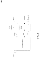
- FIG. 1 shows a block diagram of a first device having a volatile memory and control circuit, consistent with one or more embodiments.
- the device 100 includes a volatile memory circuit 110 and a control circuit 120 coupled to the volatile memory circuit.
- the control circuit 120 may include, for example, programmed or semi-programmed logic circuitry configured to provide FEC protection of data stored by the volatile memory circuit 110, by performing a process that includes generating and storing parity data for data blocks written to the volatile memory circuit. The process further places the volatile memory circuit 110 in a sleep mode in response to a first control signal. In the sleep mode, a supply voltage used to power the volatile memory is set to a voltage at which data blocks stored in the volatile memory circuit 110 are subject to an introduction of errors.
- the process performed by the control circuit 120 wakes the volatile memory circuit 110 from the sleep mode to place the circuit into an active mode in response to a second control signal.
- the process performed by the control circuit 120 corrects errors in the data blocks stored in the volatile memory using the stored parity data. In this manner the device recovers errors that may have occurred while the non-volatile memory circuit 110 is operated in the sleep mode.
- FIG. 2 shows a block diagram of a second device having a volatile memory and control circuit, consistent with one or more embodiments.
- the device 200 includes a volatile memory circuit 210 and a control circuit 220 coupled to the volatile memory circuit.
- the control circuit 220 may include, for example, programmed or semi-programmed logic circuitry configured to provide FEC protection of data stored by the volatile memory circuit 210, by performing a process that includes generating and storing parity data for data blocks written to the volatile memory circuit. The process further places the volatile memory circuit 210 in a sleep mode in response to a first control signal. In the sleep mode, a supply voltage used to power the volatile memory is set to a voltage at which data blocks stored in the volatile memory circuit 210 are subject to an introduction of errors.
- the process performed by the control circuit 220 wakes the volatile memory circuit 210 from the sleep mode to place the circuit into an active mode in response to a second control signal. In further response to the second control signal, the process performed by the control circuit 220 corrects errors in the data blocks stored in the volatile memory using the stored parity data.
- control circuit 220 places the volatile memory circuit 210 in the sleep mode by causing a lower supply voltage (Vdd Low ) to be provided to the volatile memory circuit 210. Conversely, the control circuit 220 places the volatile memory circuit 210 in the active mode by causing a higher supply voltage (Vdd High ) to be provided to the volatile memory circuit 210, where Vdd High > Vdd Low .
- the device 200 includes a selection circuit 230 configured to connect one of the voltage sources (Vdd High and Vdd Low ), indicated by a selection signal (Sel), to a power supply terminal of the volatile memory circuit 210.
- the Sel is adjusted by the control circuit 220 to place the volatile memory circuit 210 in either the active mode or the sleep mode.
- logic circuitry in the control circuit 220 may set the Sel signal to a first binary value (e.g., logic 0)-thereby directing the selection circuit 230 to provide Vdd Low to the volatile memory circuit 210.
- the logic circuitry in the control circuit 220 may set the Sel signal to a second binary value (e.g., logic 1)-thereby directing the selection circuit 230 to provide Vdd High to the volatile memory circuit 210.
- the selection circuit 230 may be implemented with various circuit arrangements.
- the selection circuit may include respective transistors to couple a respective supply voltage to a power supply terminal of the volatile memory circuit 210, in response to the Sel signal.
- the selection circuit 230 may include an n-type transistor having a source terminal coupled to Vdd High , a drain terminal coupled to the power supply terminal of the volatile memory circuit 210, and a gate terminal coupled to receive the Sel signal.
- the selection circuit 230 may include an p-type transistor having a source terminal coupled to Vdd Low , a drain terminal coupled to the power supply terminal of the volatile memory circuit 210, and a gate terminal coupled to receive the Sel signal.
- the n-type transistor When Sel is set to logic 1, the n-type transistor connects Vdd High to the power supply terminal and the p-type transistor disconnects Vdd Low from the power supply terminal. Conversely, when Sel is set to logic 0, the n-type transistor disconnects Vdd High from the power supply terminal and the p-type transistor connects Vdd Low to the power supply terminal.
- control circuit may be configured adjust a voltage output by a programmable voltage source connected to the volatile memory circuits.
- Logic circuitry e.g., a programmed processor
- the control circuit 220 may specify a voltage value in the Sel signal provided to the programmable voltage source-thereby directing the programmable voltage source to provide the specified voltage to the volatile memory circuit 210.
- logic circuitry of the control circuit may place the volatile memory circuit 210 in the sleep mode by setting the output signal Sel to specify the lower-voltage level.
- logic circuitry of the control circuit 220 may place the volatile memory circuit 210 in the active mode by setting the output signal Sel to specify the higher-voltage level.
- the control circuit 220 is configured to generate and store FEC parity data for data blocks written to the volatile memory circuit 210.
- the FEC parity data is used to correct errors in the volatile memory when it is placed back into the active mode from the sleep mode. For instance, in response to the second control signal, the control circuit may check each data block stored in the volatile memory 210 using the parity data previously generated by the control circuit 220 for the data block.
- control circuit 220 includes an FEC encoder 222 configured to generate FEC parity data for each data block written to the volatile memory circuit 210.
- the control circuit 220 also includes an FEC decoder 224 configured to detect and correct errors in data blocks retrieved from the volatile memory circuit 210 using the parity data previously generated for the data block by the FEC encoder 222.
- the FEC parity data may be stored in the volatile memory circuit 210 or may be stored in a different memory (e.g., that may be included in the control circuit 220).
- control circuit 220 is configured to correct errors in the volatile memory using the FEC parity data when it is placed into the active mode from the sleep mode.
- FEC may also be used to correct a limited number of errors in the volatile memory circuit in the active mode.
- the control circuit 220 may use a lower-latency lower-error-rate FEC code to correct errors incurred while the non-volatile memory is in the active mode.
- the control circuit 220 may use a higher-latency high-error-rate FEC code to correct errors incurred while the volatile memory 210 is in the sleep mode.
- the control circuit 220 may utilize various FEC codes along or in combination to correct errors induced while the volatile memory 210 is operated in the sleep and/or active modes.
- FIG. 3 shows a state machine that may be used by a control circuit for a volatile memory.
- state 330 the volatile memory is operated in an active mode, as described with reference to FIGs. 1 and 2 .
- state 310 where the volatile memory is operated in a sleep mode, as described with reference to FIGs. 1 and 2 .
- state machine transfers to state 320, where a set of resume processes are performed.
- the resume processes correct errors in data block stored in the volatile memory at sub-state 322 and write corrected data blocks back to the volatile memory at sub-state 324.
- the state machine transitions back to state 330 and the volatile memory is again operated in the active mode.
- different embodiment may use various techniques to adjust the supply voltage provided to the volatile memory in the sleep mode. For example, some embodiments may set the supply voltage to a fixed voltage level (e.g., indicated in a non-volatile memory). Some other embodiments, may dynamically adjust the sleep mode supply voltage based on the error rate exhibited by the volatile memory for previous supply voltages.
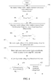
- FIG. 4 shows a process for operating a volatile memory that dynamically determines a supply voltage level for sleep mode operation, consistent with one or more embodiments.
- a supply voltage provided to the volatile memory is set to an active mode level to place the non-volatile memory in an active mode.
- the active mode level is specified in a non-volatile memory.
- the active mode level may correspond to a highest level provided by a programmable voltage supply.
- the non-volatile memory operates in the active mode, until a sleep command is received at decision block 406. Once a sleep command is received, decision block 406 directs the process to block 408. At block 408, the supply voltage provided to the memory circuit is decreased to a sleep mode level to place the non-volatile memory in a sleep mode. The non-volatile memory operates in the sleep mode, until a resume command is received at decision block 410. Once the resume command is received, decision block 410 directs the process to block 412.
- the supply voltage provided to the volatile memory is increased back to the active mode level to place the non-volatile memory back in an active mode.
- errors in data blocks stored in the volatile memory are detected and corrected using FEC parity data.
- sleep mode voltage level is adjusted based on the number of error detected in the volatile memory. In this example, if the number of detected errors is less than a lower threshold, decision block 420 directs the process to decrease the sleep mode voltage level at block 422. Lowering the sleep mode voltage level allows power consumption in the sleep mode to be reduced until the number of induced errors nears that maximum number of errors that may be corrected using the FEC parity data.
- the adjustment at block 418 may be configured to also increase the sleep mode voltage level if the number of detected errors exceeds an upper threshold.
- Use of the upper threshold may be useful to prevent changing environmental conditions from causing the number of errors to exceed the maximum number of errors that may be corrected using FEC the parity data.
- FIG. 5 shows a process for operating a volatile memory in an active mode, consistent with one or more embodiments.
- the process may be performed, for example, by control circuit 120 and 220 in FIGs. 1 and 2 while the volatile memory circuits are operated in the active mode.
- the process starts when a transaction 502 is initiated. If the transaction is a write transaction, decision block 504 directs the process to block 510.
- parity data is generated for a higher-latency FEC code used to correct errors induced while the volatile memory is operating in sleep mode 510.
- block 510 may be omitted in the active mode process, and parity data may instead be generated for all data blocks just before the volatile memory is placed into the sleep mode.
- parity data may be generated for a lower-latency FEC code at block 512.
- the lower-latency FEC code may use a subset of parity data generated for the higher-latency FEC code at block 510. In such case, it may not be necessary to generate additional parity data at block 512.
- the data block for the write transaction and parity data is stored in one or more memories. The parity data may be stored along with the data block in the volatile memory or may be stored in a separate memory. If the transaction 502 is a read transaction, decision block 504 directs the process to decision block 506. At block 506, the data block indicated by the transaction 502 is retrieved from the volatile memory. Optionally at block 508, errors may be corrected in the retrieved data block using the lower-latency FEC code.
- a "block” (also sometimes “logic circuitry” or “module”) is a circuit that carries out one or more of these or related operations/activities (e.g., generation of parity data, or FEC).
- one or more modules are discrete logic circuits or programmable logic circuits configured and arranged for implementing these operations/activities, as in the circuit modules shown in FIGs. 1 and 2 .
- such a programmable circuit is one or more computer circuits programmed to execute a set (or sets) of instructions (and/or configuration data).
- the instructions can be in the form of firmware or software stored in and accessible from a memory (circuit).
- first and second modules include a combination of a CPU hardware-based circuit and a set of instructions in the form of firmware, where the first module includes a first CPU hardware circuit with one set of instructions and the second module includes a second CPU hardware circuit with another set of instructions.
- Certain embodiments are directed to a computer program product (e.g., nonvolatile memory device), which includes a machine or computer-readable medium having stored thereon instructions which may be executed by a computer (or other electronic device) to perform these operations/activities.
- a computer program product e.g., nonvolatile memory device
Landscapes
- Engineering & Computer Science (AREA)
- Theoretical Computer Science (AREA)
- Physics & Mathematics (AREA)
- General Engineering & Computer Science (AREA)
- General Physics & Mathematics (AREA)
- Quality & Reliability (AREA)
- Techniques For Improving Reliability Of Storages (AREA)
- For Increasing The Reliability Of Semiconductor Memories (AREA)
Abstract
Aspects of the present disclosure are directed to circuits, apparatuses and methods for operating volatile memory circuits. According to an example embodiment, an apparatus includes a volatile memory circuit and a control circuit coupled to the volatile memory circuit. The control circuit is configured to generate and store parity data for data blocks written to the volatile memory circuit. The control circuit places the volatile memory circuit in a sleep mode in response to a first control signal. In response to a second control signal, the control circuit places the volatile memory into an active mode. In further response to the second control signal the control circuit detects and corrects errors in the data blocks stored in the volatile memory using the stored parity data.
Description
- This disclosure relates to volatile memory circuits.
- Power consumption is increasingly becoming a design consideration for many application, especially those involving battery operated devices. Some approaches to reduce power consumption operate circuits in a sleep or standby mode when idle, in which a power supply provided to the circuits is reduced or disconnected from the circuits. By removing or reducing the power supply, leakage current of the idle circuits can be reduced. However, systems including volatile memory may have to maintain the state of data stored in volatile memory circuits when operated in a sleep mode. Volatile memory circuits are used in various applications for storage of data. Volatile memory circuits, such as SRAM cells, retain data values stored while power is applied to the memory circuits but do not maintain stored data values when power is disconnected from the memory circuit. These and other matters have presented challenges for a variety of applications utilizing volatile memory circuits.
- Various example embodiments are directed to circuits, apparatuses and methods for operating volatile memory circuits. According to an example embodiment, an apparatus includes a volatile memory circuit and a control circuit coupled to the volatile memory circuit. The control circuit is configured to generate and store parity data for data blocks written to the volatile memory circuit. The control circuit places the volatile memory circuit in a sleep mode in response to a first control signal. In the sleep mode, a supply voltage for the volatile memory is set to a first voltage, at which data blocks stored in the volatile memory circuit are subject to the introduction of errors. In response to a second control signal, the control circuit places the volatile memory into an active mode. In further response to the second control signal the control circuit detects and corrects errors in the data blocks stored in the volatile memory using the stored parity data.
- Another example embodiment provides a method for operating a volatile memory. Parity data is generated and stored for data blocks written to a volatile memory circuit. The volatile memory circuit is placed in a sleep mode in response to a first control signal. The volatile memory is placed into an active mode in response to a second control signal. In further response to the second control signal, errors in the data blocks are detected and corrected using the stored parity data.
- In another example embodiment, an apparatus includes a volatile memory circuit. The apparatus also includes a circuit means for generating and storing parity data for data blocks written to the volatile memory circuit, for placing the volatile memory circuit in a sleep mode in response to a first control signal, for placing the volatile memory into an active mode in response to a second control signal, and for detecting and correcting errors in the data blocks using the stored parity data in further response to the second control signal.
- Embodiments of the apparatus may comprise a volatile memory circuit; and a control circuit configured and arranged to generate and store parity data for data blocks written to the volatile memory circuit; in response to a first control signal, place the volatile memory circuit in a sleep mode, in which a supply voltage for the volatile memory is set to a first voltage at which data blocks stored in the volatile memory circuit are subject to an introduction of errors; and in response to a second control signal, place the volatile memory into an active mode, and detect and correct errors in the data blocks stored in the volatile memory using the stored parity data.
- In embodiments of the apparatus, placing of the volatile memory into the active mode may include setting the supply voltage to a second voltage that is greater than the first voltage and that is sufficient to prevent errors from being introduced in data blocks stored by the volatile memory.
- Embodiments of the apparatus may comprise a selection circuit configured to connect a select one of a plurality of voltage sources that is indicated by a control signal, to a supply terminal of the volatile memory circuit.
- In embodiments the parity data may be configured to correct up to N errors in each data block stored in the volatile memory; and a number of errors that is expected to be introduced in data stored by the volatile memory when the supply voltage is set to the first voltage is less than N.
- In embodiments the apparatus may comprise a non-volatile memory, and wherein the setting of the supply voltage to the first voltage sets the supply voltage to a level indicated in a value stored in the non-volatile memory.
- In embodiments of the apparatus the control circuit may be further configured and arranged to, in response to a number of errors detected in response to the second control signal being less than a first threshold value, decreasing the value stored in the non-volatile memory.
- In embodiments, the control circuit may be further configured and arranged to, in response to the number of errors detected in response to the second control signal being greater than a second threshold value, increasing the value stored in the non-volatile memory.
- In embodiments the parity data may be stored in the volatile memory circuit.
- In embodiments, the apparatus may comprise a second memory circuit; and wherein the control circuit is configured to store the parity data in the second memory circuit.
- In embodiments, the control circuit may be configured to, in response to a data block being read from the volatile memory in the active mode, detect and recover from errors in the data block using the parity data.
- In embodiments the detection and recovery of errors by the control circuit in response to the data block being read may be performed using a first error correction code configured to correct up to a first number of errors; and the detection and recovery of errors by the control circuit in response to the second control signal is performed using a second error correction code configured to correct up to a second number of errors that is greater than the first number of errors.
- In embodiments the placing of the volatile memory into the active mode may include setting the supply voltage to a second voltage that is greater than the first voltage and that is sufficient to prevent more than the first number of errors from being introduced in data blocks stored by the volatile memory.
- In embodiments the second error correction code may use a first number bits of the parity data for detection and recovery of errors of a data block stored in the volatile memory; and the first error correction code uses a subset of the first number of bits for detection and recovery of errors of the data block.
- The second error correction code may be concatenated code including Reed-Solomon correction code and BCH correction code; and the first error correction code may be one of Reed-Solomon correction code or BCH correction code.
- Embodiments may comprise a method, comprising generating and storing parity data for data blocks written to a volatile memory circuit; in response to a first control signal, placing the volatile memory circuit in a sleep mode; and in response to a second control signal placing the volatile memory into an active mode, and detecting and correcting errors in the data blocks stored in the volatile memory using the stored parity data.
- In embodiments the placing of the volatile memory in the active mode may include setting a supply voltage for the volatile memory to a first voltage sufficient to prevent errors from being introduced in data stored by the volatile memory; and the placing of the volatile memory in the active mode may include setting the supply voltage to a second lower voltage at which errors are introduced in the data blocks stored by the volatile memory circuit.
- In embodiments, the setting of the supply voltage to the second lower voltage may set the supply voltage to a level indicated in a value stored in a non-volatile memory; and may further comprise decreasing the value stored in the non-volatile memory in response to a number of detected errors being less than a first threshold value, and increasing the value stored in the non-volatile memory in response to the number of detected errors being greater than a second threshold value, increasing the value stored in the non-volatile memory.
- Embodiments may further comprise in response to a data block being read from the volatile memory in the active mode, detecting and recovering from errors in the data block using the parity data.
- The detection and recovery of errors in response to the data block being read may be performed using a first error correction code configured to correct up to a first number of errors; and the detection and recovery of errors in response to the second control signal may be performed using a second error correction code configured to correct up to a second number of errors that is greater than the first number of errors.
- Embodiments of the apparatus may comprise a volatile memory circuit; and a circuit means for generating and storing parity data for data blocks written to the volatile memory circuit, placing the volatile memory circuit in a sleep mode in response to a first control signal and, in response to a second control signal, placing the volatile memory into an active mode and detecting and correcting errors in the data blocks stored in the volatile memory using the stored parity data.
- In embodiments the apparatus may include a volatile memory circuit and a control circuit coupled to the volatile memory circuit. The control circuit may be configured to generate and store parity data for data blocks written to the volatile memory circuit. The control circuit may places the volatile memory circuit in a sleep mode in response to a first control signal. In response to a second control signal, the control circuit may place the volatile memory into an active mode. In further response to the second control signal the control circuit may detect and correct errors in the data blocks stored in the volatile memory using the stored parity data.
- The above discussion/summary is not intended to describe each embodiment or every implementation of the present disclosure. The figures and detailed description that follow also exemplify various embodiments.
- Various example embodiments may be more completely understood in consideration of the following detailed description in connection with the accompanying drawings, in which:
-
FIG. 1 shows a block diagram of a first device having a volatile memory and control circuit, consistent with one or more embodiments; -
FIG. 2 shows a block diagram of a second device having a volatile memory and control circuit, consistent with one or more embodiments; -
FIG. 3 shows a state machine that may be used by a control circuit for a volatile memory, consistent with one or more embodiments; -
FIG. 4 shows a process for operating a volatile memory, consistent with one or more embodiments; and -
FIG. 5 shows a process for operating a volatile memory in an active mode, consistent with one or more embodiments. - While various embodiments discussed herein are amenable to modifications and alternative forms, aspects thereof have been shown by way of example in the drawings and will be described in detail. It should be understood, however, that the intention is not to limit the invention to the particular embodiments described. On the contrary, the intention is to cover all modifications, equivalents, and alternatives falling within the scope of the disclosure including aspects defined in the claims. In addition, the term "example" as used throughout this application is only by way of illustration, and not limitation.
- Aspects of the present disclosure are believed to be applicable to a variety of different types of apparatuses, systems and methods involving volatile memory circuits. Some aspects are particularly applicable to apparatuses, systems and methods having a sleep mode for reduced power consumption. While not necessarily so limited, various aspects may be appreciated through a discussion of examples using this context.
- Volatile memory circuits such as SRAM require a certain threshold supply voltage to prevent the introduction of errors beyond a maximum number that can be handled by the volatile memory circuits in an active mode. The number of errors introduced increases as the supply voltage is decreased. Various embodiments utilize forward error correction (FEC) codes to facilitate recovery of a number of errors, when waking from a sleep mode that is larger than the maximum can be handled by the memory circuits in the active mode. The ability to recover from a larger number of errors allows a supply voltage for the volatile memory circuit to be further reduced in the sleep mode while maintaining the ability to recover from errors that may be introduced.
- FEC codes generate redundant data, referred to as parity data, for data blocks prior to storage or transmission. After transmission or storage of a data block, the FEC code uses the parity data to detect and/or recover errors present in the data block. Some example FEC codes include Hamming, Bose-Chaudhuri-Hochquenghem (BCH), Reed-Solomon, Trellis, and/or convolutional codes. Some error correction techniques use a combination of two or more FEC codes to increase the number of errors that can be recovered. One example combination, specified in ITU-T G.975.1 I.4, implements a concatenation of Reed-Solomon and BCH encoding schemes.
- In some embodiments, an apparatus includes a volatile memory circuit and a control circuit coupled to the volatile memory circuit. The control circuit is configured to generate and store parity data for data blocks written to the volatile memory circuit. The control circuit reduces a supply voltage provided to the volatile memory circuit, in response to a first control signal, to place the volatile memory circuit in a sleep mode. The control circuit increases a supply voltage provided to the volatile memory circuit, in response to a second control signal, to place the volatile memory circuit in an active mode. In further response to the second control signal the control circuit detects and corrects errors in the data blocks stored in the volatile memory using the stored parity data.
- In some applications, FEC may also be used to prevent introduction of errors in the volatile memory circuit when operated in the active mode. For instance, FEC parity data may be generated when a data block is written to the volatile memory and used to correct errors when the data block is read from the volatile memory. However, the generating of FEC parity data and the recovery from errors takes a certain amount of processing time to be performed. Generally speaking, the processing time required for encoding and decoding operations increases as the number of parity bits used by the error correction code (and the number of errors that can be corrected) is increased. As applications often require memories to exhibit low latency for read times, the processing time needed for recovery for a large number of errors using FEC may be prohibitive.
- In some embodiments, a control circuit is configured to use a lower-latency low-error-rate FEC code when the volatile memory is operated in the active mode and a higher-latency high-error-rate FEC code when the volatile memory is operated in the sleep mode. The high-error-rate FEC code allows for recover from a larger number of errors introduced while operating the volatile memory in the sleep mode at the expense of increased latency. However, from user perspective, a certain amount of latency is generally expected and tolerated as a one-time expense when waking from the sleep mode and restoring the state of a system. By using the higher-latency high-error-rate FEC code in the sleep mode, a supply voltage for the volatile memory may be reduced in the sleep mode in comparison to a supply voltage required for operation in the active mode.
- Various FEC codes may be used to correct errors induced in the sleep and/or active modes. In some implementations, the lower-latency low-error-rate FEC code may recover from errors using a subset of the parity data used by the higher-latency high-error-rate FEC code.
- For example, the two FEC codes may use the same encoding algorithm with a different number of parity bits. As another example, the higher-latency high-error-rate FEC code may include a concatenation of two FEC codes (e.g., Reed-Solomon and BCH) with separate sets of parity data generated for each of the two FEC codes. The lower-latency low-error-rate FEC code may perform error correction using parity data for one of the two concatenated FEC codes. In some other implementations, the lower-latency low-error-rate FEC code and the higher-latency high-error-rate FEC code use mutually exclusive sets of parity data. The parity data for the FEC code(s) may be stored in the volatile memory or may be stored in a separate volatile or non-volatile memory
- In some embodiments, the control circuit may reduce a supply voltage, when operated in the sleep mode, below that required by the volatile memory to prevent errors from being introduced. For example, when operating the volatile memory in the active mode, the control circuit may set the supply voltage for the volatile memory to a first voltage sufficient to prevent errors from being introduced in data stored by the volatile memory. When operating the volatile memory in the sleep mode, the control circuit may reduce the supply voltage to a second lower voltage at which errors may be introduced in the data stored by the volatile memory circuit.
- Different embodiment may utilize various circuits to adjust the voltage source provided to the volatile memory. In one embodiment, the apparatus may include a selection circuit configured to connect a selected one of a plurality of voltage sources to volatile memory. The selected one of the voltage sources may be indicated by, for example, a control signal output from control circuit. In another embodiment, the control circuit may be configured to adjust a voltage output by a programmable voltage source connected to the volatile memory circuits.
- In some implementations, the control circuit may set the voltage source for the sleep mode to a fixed voltage level indicated by a value stored in the non-volatile memory. In some other embodiments, the control circuit may dynamically adjust the voltage level of the voltage source based on the rate at which errors are detected. For instance, the control circuit may determine a voltage level for the sleep mode based on a number of errors previously detected when awakening from the sleep mode and a maximum number of errors that can be recovered by the FEC code.
- Turning now to the figures,
FIG. 1 shows a block diagram of a first device having a volatile memory and control circuit, consistent with one or more embodiments. Thedevice 100 includes avolatile memory circuit 110 and acontrol circuit 120 coupled to the volatile memory circuit. Thecontrol circuit 120 may include, for example, programmed or semi-programmed logic circuitry configured to provide FEC protection of data stored by thevolatile memory circuit 110, by performing a process that includes generating and storing parity data for data blocks written to the volatile memory circuit. The process further places thevolatile memory circuit 110 in a sleep mode in response to a first control signal. In the sleep mode, a supply voltage used to power the volatile memory is set to a voltage at which data blocks stored in thevolatile memory circuit 110 are subject to an introduction of errors. The process performed by thecontrol circuit 120 wakes thevolatile memory circuit 110 from the sleep mode to place the circuit into an active mode in response to a second control signal. In further response to the second control signal, the process performed by thecontrol circuit 120 corrects errors in the data blocks stored in the volatile memory using the stored parity data. In this manner the device recovers errors that may have occurred while thenon-volatile memory circuit 110 is operated in the sleep mode. -
FIG. 2 shows a block diagram of a second device having a volatile memory and control circuit, consistent with one or more embodiments. Thedevice 200 includes avolatile memory circuit 210 and acontrol circuit 220 coupled to the volatile memory circuit. Thecontrol circuit 220 may include, for example, programmed or semi-programmed logic circuitry configured to provide FEC protection of data stored by thevolatile memory circuit 210, by performing a process that includes generating and storing parity data for data blocks written to the volatile memory circuit. The process further places thevolatile memory circuit 210 in a sleep mode in response to a first control signal. In the sleep mode, a supply voltage used to power the volatile memory is set to a voltage at which data blocks stored in thevolatile memory circuit 210 are subject to an introduction of errors. The process performed by thecontrol circuit 220 wakes thevolatile memory circuit 210 from the sleep mode to place the circuit into an active mode in response to a second control signal. In further response to the second control signal, the process performed by thecontrol circuit 220 corrects errors in the data blocks stored in the volatile memory using the stored parity data. - In this example, the
control circuit 220 places thevolatile memory circuit 210 in the sleep mode by causing a lower supply voltage (VddLow) to be provided to thevolatile memory circuit 210. Conversely, thecontrol circuit 220 places thevolatile memory circuit 210 in the active mode by causing a higher supply voltage (VddHigh) to be provided to thevolatile memory circuit 210, where VddHigh > VddLow. - When the volatile memory circuit is operated at the voltage of the lower supply voltage data blocks stored in the volatile memory circuit are subject to an introduction of errors. As previously discussed, the lower supply voltage provided to the
volatile memory circuit 210 in the sleep mode may be a voltage level at which the number of errors that are induced is greater than can be handled by thevolatile memory circuit 210 in the active mode. In this example, thedevice 200 includes aselection circuit 230 configured to connect one of the voltage sources (VddHigh and VddLow), indicated by a selection signal (Sel), to a power supply terminal of thevolatile memory circuit 210. The Sel is adjusted by thecontrol circuit 220 to place thevolatile memory circuit 210 in either the active mode or the sleep mode. For instance, in some implementations, logic circuitry (e.g., for example programmed or semi-programmed logic circuitry) in thecontrol circuit 220 may set the Sel signal to a first binary value (e.g., logic 0)-thereby directing theselection circuit 230 to provide VddLow to thevolatile memory circuit 210. Conversely, the logic circuitry in thecontrol circuit 220 may set the Sel signal to a second binary value (e.g., logic 1)-thereby directing theselection circuit 230 to provide VddHigh to thevolatile memory circuit 210. - The
selection circuit 230 may be implemented with various circuit arrangements. As one example, the selection circuit may include respective transistors to couple a respective supply voltage to a power supply terminal of thevolatile memory circuit 210, in response to the Sel signal. For instance, theselection circuit 230 may include an n-type transistor having a source terminal coupled to VddHigh, a drain terminal coupled to the power supply terminal of thevolatile memory circuit 210, and a gate terminal coupled to receive the Sel signal. Theselection circuit 230 may include an p-type transistor having a source terminal coupled to VddLow, a drain terminal coupled to the power supply terminal of thevolatile memory circuit 210, and a gate terminal coupled to receive the Sel signal. When Sel is set to logic 1, the n-type transistor connects VddHigh to the power supply terminal and the p-type transistor disconnects VddLow from the power supply terminal. Conversely, when Sel is set to logic 0, the n-type transistor disconnects VddHigh from the power supply terminal and the p-type transistor connects VddLow to the power supply terminal. - In some other embodiments, the control circuit may be configured adjust a voltage output by a programmable voltage source connected to the volatile memory circuits. Logic circuitry (e.g., a programmed processor) in the
control circuit 220 may specify a voltage value in the Sel signal provided to the programmable voltage source-thereby directing the programmable voltage source to provide the specified voltage to thevolatile memory circuit 210. For instance, logic circuitry of the control circuit may place thevolatile memory circuit 210 in the sleep mode by setting the output signal Sel to specify the lower-voltage level. Conversely, logic circuitry of thecontrol circuit 220 may place thevolatile memory circuit 210 in the active mode by setting the output signal Sel to specify the higher-voltage level. - The
control circuit 220 is configured to generate and store FEC parity data for data blocks written to thevolatile memory circuit 210. The FEC parity data is used to correct errors in the volatile memory when it is placed back into the active mode from the sleep mode. For instance, in response to the second control signal, the control circuit may check each data block stored in thevolatile memory 210 using the parity data previously generated by thecontrol circuit 220 for the data block. - In this example, the
control circuit 220 includes anFEC encoder 222 configured to generate FEC parity data for each data block written to thevolatile memory circuit 210. Thecontrol circuit 220 also includes anFEC decoder 224 configured to detect and correct errors in data blocks retrieved from thevolatile memory circuit 210 using the parity data previously generated for the data block by theFEC encoder 222. The FEC parity data may be stored in thevolatile memory circuit 210 or may be stored in a different memory (e.g., that may be included in the control circuit 220). - As previously indicated, the
control circuit 220 is configured to correct errors in the volatile memory using the FEC parity data when it is placed into the active mode from the sleep mode. In some applications, FEC may also be used to correct a limited number of errors in the volatile memory circuit in the active mode. For instance, thecontrol circuit 220 may use a lower-latency lower-error-rate FEC code to correct errors incurred while the non-volatile memory is in the active mode. Thecontrol circuit 220 may use a higher-latency high-error-rate FEC code to correct errors incurred while thevolatile memory 210 is in the sleep mode. Thecontrol circuit 220, may utilize various FEC codes along or in combination to correct errors induced while thevolatile memory 210 is operated in the sleep and/or active modes. -
FIG. 3 shows a state machine that may be used by a control circuit for a volatile memory. Instate 330, the volatile memory is operated in an active mode, as described with reference toFIGs. 1 and2 . In response to a sleep command, the state machine transitions tostate 310, where the volatile memory is operated in a sleep mode, as described with reference toFIGs. 1 and2 . In response to a resume command, the state machine transfers tostate 320, where a set of resume processes are performed. In this example, the resume processes correct errors in data block stored in the volatile memory atsub-state 322 and write corrected data blocks back to the volatile memory atsub-state 324. After completing the resume process atstate 320 the state machine transitions back tostate 330 and the volatile memory is again operated in the active mode. - As previously indicated, different embodiment may use various techniques to adjust the supply voltage provided to the volatile memory in the sleep mode. For example, some embodiments may set the supply voltage to a fixed voltage level (e.g., indicated in a non-volatile memory). Some other embodiments, may dynamically adjust the sleep mode supply voltage based on the error rate exhibited by the volatile memory for previous supply voltages.
-
FIG. 4 shows a process for operating a volatile memory that dynamically determines a supply voltage level for sleep mode operation, consistent with one or more embodiments. Atblock 402, a supply voltage provided to the volatile memory is set to an active mode level to place the non-volatile memory in an active mode. In some implementations, the active mode level is specified in a non-volatile memory. In some other implementations, the active mode level may correspond to a highest level provided by a programmable voltage supply. - The non-volatile memory operates in the active mode, until a sleep command is received at
decision block 406. Once a sleep command is received,decision block 406 directs the process to block 408. Atblock 408, the supply voltage provided to the memory circuit is decreased to a sleep mode level to place the non-volatile memory in a sleep mode. The non-volatile memory operates in the sleep mode, until a resume command is received atdecision block 410. Once the resume command is received,decision block 410 directs the process to block 412. - At
block 412, the supply voltage provided to the volatile memory is increased back to the active mode level to place the non-volatile memory back in an active mode. Atblock 414, errors in data blocks stored in the volatile memory are detected and corrected using FEC parity data. Atblock 418, sleep mode voltage level is adjusted based on the number of error detected in the volatile memory. In this example, if the number of detected errors is less than a lower threshold,decision block 420 directs the process to decrease the sleep mode voltage level atblock 422. Lowering the sleep mode voltage level allows power consumption in the sleep mode to be reduced until the number of induced errors nears that maximum number of errors that may be corrected using the FEC parity data. In some embodiments, the adjustment atblock 418 may be configured to also increase the sleep mode voltage level if the number of detected errors exceeds an upper threshold. Use of the upper threshold may be useful to prevent changing environmental conditions from causing the number of errors to exceed the maximum number of errors that may be corrected using FEC the parity data. -
FIG. 5 shows a process for operating a volatile memory in an active mode, consistent with one or more embodiments. The process may be performed, for example, bycontrol circuit FIGs. 1 and2 while the volatile memory circuits are operated in the active mode. The process starts when atransaction 502 is initiated. If the transaction is a write transaction,decision block 504 directs the process to block 510. Atblock 510, parity data is generated for a higher-latency FEC code used to correct errors induced while the volatile memory is operating insleep mode 510. Alternatively, in some embodiments, block 510 may be omitted in the active mode process, and parity data may instead be generated for all data blocks just before the volatile memory is placed into the sleep mode. - Optionally, if FEC is performed in the active mode, parity data may be generated for a lower-latency FEC code at
block 512. However, as previously described, in some implementations, the lower-latency FEC code may use a subset of parity data generated for the higher-latency FEC code atblock 510. In such case, it may not be necessary to generate additional parity data atblock 512. Atblock 514, the data block for the write transaction and parity data is stored in one or more memories. The parity data may be stored along with the data block in the volatile memory or may be stored in a separate memory. If thetransaction 502 is a read transaction,decision block 504 directs the process todecision block 506. Atblock 506, the data block indicated by thetransaction 502 is retrieved from the volatile memory. Optionally atblock 508, errors may be corrected in the retrieved data block using the lower-latency FEC code. - Various blocks, modules or other circuits may be implemented to carry out one or more of the operations and activities described herein and/or shown in the figures. In these contexts, a "block" (also sometimes "logic circuitry" or "module") is a circuit that carries out one or more of these or related operations/activities (e.g., generation of parity data, or FEC). For example, in certain of the above-discussed embodiments, one or more modules are discrete logic circuits or programmable logic circuits configured and arranged for implementing these operations/activities, as in the circuit modules shown in
FIGs. 1 and2 . In certain embodiments, such a programmable circuit is one or more computer circuits programmed to execute a set (or sets) of instructions (and/or configuration data). The instructions (and/or configuration data) can be in the form of firmware or software stored in and accessible from a memory (circuit). As an example, first and second modules include a combination of a CPU hardware-based circuit and a set of instructions in the form of firmware, where the first module includes a first CPU hardware circuit with one set of instructions and the second module includes a second CPU hardware circuit with another set of instructions. - Certain embodiments are directed to a computer program product (e.g., nonvolatile memory device), which includes a machine or computer-readable medium having stored thereon instructions which may be executed by a computer (or other electronic device) to perform these operations/activities.
- Based upon the above discussion and illustrations, those skilled in the art will readily recognize that various modifications and changes may be made to the various embodiments without strictly following the exemplary embodiments and applications illustrated and described herein. For instance, although implementations may in some cases be described in individual figures, it will be appreciated that features from one figure can be combined with features from another figure even though the combination is not explicitly shown or explicitly described as a combination. Such modifications do not depart from the true spirit and scope of various aspects of the invention, including aspects set forth in the claims.
Claims (15)
- An apparatus, comprising:a volatile memory circuit; anda control circuit configured and arranged to
generate and store parity data for data blocks written to the volatile memory circuit;
in response to a first control signal, place the volatile memory circuit in a sleep mode, in which a supply voltage for the volatile memory is set to a first voltage at which data blocks stored in the volatile memory circuit are subject to an introduction of errors; and
in response to a second control signal,
place the volatile memory into an active mode, and
detect and correct errors in the data blocks stored in the volatile memory using the stored parity data. - The apparatus of claim 1, wherein placing of the volatile memory into the active mode includes setting the supply voltage to a second voltage that is greater than the first voltage and that is sufficient to prevent errors from being introduced in data blocks stored by the volatile memory.
- The apparatus of claim 1 or 2, further comprising, a selection circuit configured to connect a select one of a plurality of voltage sources, that is indicated by a control signal, to a supply terminal of the volatile memory circuit.
- The apparatus of any preceding claim, wherein
the parity data is configured to correct up to N errors in each data block stored in the volatile memory; and
a number of errors that is expected to be introduced in data stored by the volatile memory when the supply voltage is set to the first voltage is less than N. - The apparatus of any preceding claim, further comprising a non-volatile memory, and wherein the setting of the supply voltage to the first voltage sets the supply voltage to a level indicated in a value stored in the non-volatile memory.
- The apparatus of claim 5, wherein the control circuit is further configured and arranged to, in response to a number of errors detected in response to the second control signal being less than a first threshold value, decreasing the value stored in the non-volatile memory.
- The apparatus of claim 5 or 6, wherein the control circuit is further configured and arranged to, in response to the number of errors detected in response to the second control signal being greater than a second threshold value, increasing the value stored in the non-volatile memory.
- The apparatus of any preceding claim, wherein the parity data is stored in the volatile memory circuit.
- The apparatus of any of claims 1 to 7, further comprising a second memory circuit; and wherein the control circuit is configured to store the parity data in the second memory circuit.
- The apparatus of any preceding claim, wherein the control circuit is further configured to, in response to a data block being read from the volatile memory in the active mode, detect and recover from errors in the data block using the parity data.
- The apparatus of claim 10, wherein:the detection and recovery of errors by the control circuit in response to the data block being read is performed using a first error correction code configured to correct up to a first number of errors; andthe detection and recovery of errors by the control circuit in response to the second control signal is performed using a second error correction code configured to correct up to a second number of errors that is greater than the first number of errors.
- The apparatus of claim 11, wherein the placing of the volatile memory into the active mode includes setting the supply voltage to a second voltage that is greater than the first voltage and that is sufficient to prevent more than the first number of errors from being introduced in data blocks stored by the volatile memory.
- The apparatus of claim 11 or 12, wherein:the second error correction code uses a first number bits of the parity data for detection and recovery of errors of a data block stored in the volatile memory; andthe first error correction code uses a subset of the first number of bits for detection and recovery of errors of the data block.
- The apparatus of claim 13, wherein
the second error correction code is concatenated code including Reed-Solomon correction code and BCH correction code; and
the first error correction code is one of Reed-Solomon correction code or BCH correction code. - A method, comprising:generating and storing parity data for data blocks written to a volatile memory circuit;in response to a first control signal, placing the volatile memory circuit in a sleep mode; andin response to a second control signal
placing the volatile memory into an active mode, and
detecting and correcting errors in the data blocks stored in the volatile memory using the stored parity data.
Applications Claiming Priority (1)
| Application Number | Priority Date | Filing Date | Title |
|---|---|---|---|
| US14/535,970 US9703632B2 (en) | 2014-11-07 | 2014-11-07 | Sleep mode operation for volatile memory circuits |
Publications (1)
| Publication Number | Publication Date |
|---|---|
| EP3018586A1 true EP3018586A1 (en) | 2016-05-11 |
Family
ID=54359954
Family Applications (1)
| Application Number | Title | Priority Date | Filing Date |
|---|---|---|---|
| EP15190738.3A Withdrawn EP3018586A1 (en) | 2014-11-07 | 2015-10-21 | Sleep mode operation for volatile memory circuits |
Country Status (3)
| Country | Link |
|---|---|
| US (1) | US9703632B2 (en) |
| EP (1) | EP3018586A1 (en) |
| CN (1) | CN105590654A (en) |
Families Citing this family (9)
| Publication number | Priority date | Publication date | Assignee | Title |
|---|---|---|---|---|
| US9495000B1 (en) * | 2015-04-30 | 2016-11-15 | Qualcomm Technologies International, Ltd. | Power management of a wireless device |
| US10223197B2 (en) | 2015-08-06 | 2019-03-05 | Nxp B.V. | Integrated circuit device and method for applying error correction to SRAM memory |
| US10437666B2 (en) | 2015-08-06 | 2019-10-08 | Nxp B.V. | Integrated circuit device and method for reading data from an SRAM memory |
| US9778983B2 (en) | 2015-08-06 | 2017-10-03 | Nxp B.V. | Integrated circuit device and method for reducing SRAM leakage |
| KR102835731B1 (en) * | 2018-12-20 | 2025-07-18 | 에스케이하이닉스 주식회사 | Apparatuses that detect error of data stored in memory device and operating method thereof |
| KR102711403B1 (en) * | 2019-03-27 | 2024-09-30 | 에스케이하이닉스 주식회사 | Controller and operating method thereof |
| US11112983B2 (en) * | 2019-08-28 | 2021-09-07 | Micron Technology, Inc. | Recovery of memory device from a reduced power state |
| US11854587B2 (en) * | 2021-12-03 | 2023-12-26 | Taiwan Semiconductor Manufacturing Company, Ltd. | Low power wake up for memory |
| CN119339751A (en) * | 2023-07-19 | 2025-01-21 | 美光科技公司 | Voltage scaling based on error rate |
Citations (3)
| Publication number | Priority date | Publication date | Assignee | Title |
|---|---|---|---|---|
| US20080222483A1 (en) * | 2007-03-08 | 2008-09-11 | Micron Technology, Inc. | Method, system, and apparatus for distributed decoding during prolonged refresh |
| US20100146368A1 (en) * | 2008-12-09 | 2010-06-10 | Chishti Zeshan A | Performing multi-bit error correction on a cache line |
| EP2560074A1 (en) * | 2011-08-17 | 2013-02-20 | Broadcom Corporation | Adaptive ultra-low voltage memory |
Family Cites Families (12)
| Publication number | Priority date | Publication date | Assignee | Title |
|---|---|---|---|---|
| US5134616A (en) * | 1990-02-13 | 1992-07-28 | International Business Machines Corporation | Dynamic ram with on-chip ecc and optimized bit and word redundancy |
| KR960000681B1 (en) * | 1992-11-23 | 1996-01-11 | 삼성전자주식회사 | Semiconductor memory device and memory array arrangement method |
| JP2002056671A (en) * | 2000-08-14 | 2002-02-22 | Hitachi Ltd | Data holding method of dynamic RAM and semiconductor integrated circuit device |
| DE102005035661A1 (en) * | 2005-07-29 | 2007-02-01 | Infineon Technologies Ag | Semiconductor memory device system, and method of operating a semiconductor memory device system |
| DE102005060901A1 (en) * | 2005-12-20 | 2007-06-28 | Robert Bosch Gmbh | A method of detecting a supply interruption in a data store and restoring the data store |
| US7840876B2 (en) * | 2007-02-20 | 2010-11-23 | Qimonda Ag | Power savings for memory with error correction mode |
| JP4564520B2 (en) * | 2007-08-31 | 2010-10-20 | 株式会社東芝 | Semiconductor memory device and control method thereof |
| CN101499325B (en) * | 2008-02-03 | 2012-10-03 | 深圳艾科创新微电子有限公司 | Non-volatile memory system and method with variable error correcting capability |
| US8352819B2 (en) * | 2009-04-15 | 2013-01-08 | Arm Limited | State retention using a variable retention voltage |
| US8640005B2 (en) * | 2010-05-21 | 2014-01-28 | Intel Corporation | Method and apparatus for using cache memory in a system that supports a low power state |
| KR101882681B1 (en) * | 2011-10-27 | 2018-07-31 | 삼성전자 주식회사 | Memory device and driving method thereof |
| KR20140071639A (en) * | 2012-12-04 | 2014-06-12 | 에스케이하이닉스 주식회사 | Semiconductor memory device improving operating speed and data storage device including the same |
-
2014
- 2014-11-07 US US14/535,970 patent/US9703632B2/en active Active
-
2015
- 2015-10-21 EP EP15190738.3A patent/EP3018586A1/en not_active Withdrawn
- 2015-11-05 CN CN201510745558.7A patent/CN105590654A/en active Pending
Patent Citations (3)
| Publication number | Priority date | Publication date | Assignee | Title |
|---|---|---|---|---|
| US20080222483A1 (en) * | 2007-03-08 | 2008-09-11 | Micron Technology, Inc. | Method, system, and apparatus for distributed decoding during prolonged refresh |
| US20100146368A1 (en) * | 2008-12-09 | 2010-06-10 | Chishti Zeshan A | Performing multi-bit error correction on a cache line |
| EP2560074A1 (en) * | 2011-08-17 | 2013-02-20 | Broadcom Corporation | Adaptive ultra-low voltage memory |
Also Published As
| Publication number | Publication date |
|---|---|
| US20160132391A1 (en) | 2016-05-12 |
| CN105590654A (en) | 2016-05-18 |
| US9703632B2 (en) | 2017-07-11 |
Similar Documents
| Publication | Publication Date | Title |
|---|---|---|
| US9703632B2 (en) | Sleep mode operation for volatile memory circuits | |
| US9170876B1 (en) | Method and system for decoding encoded data stored in a non-volatile memory | |
| US9128858B1 (en) | Apparatus and method for adjusting a correctable raw bit error rate limit in a memory system using strong log-likelihood (LLR) values | |
| US9448881B1 (en) | Memory controller and integrated circuit device for correcting errors in data read from memory cells | |
| US20110231738A1 (en) | Error correction decoding apparatus and error correction decoding method | |
| KR100645058B1 (en) | Memory Management Techniques to Improve Data Reliability | |
| US8751896B2 (en) | Semiconductor storage device, method of controlling the same, and error correction system | |
| US10067824B2 (en) | Error processing method, memory storage device and memory controlling circuit unit | |
| EP2186004B1 (en) | Semiconductor memory device and method of controlling the same | |
| US8321760B2 (en) | Semiconductor memory device and data processing method thereof | |
| US8713411B2 (en) | Encoding and/or decoding memory devices and methods thereof | |
| US20140149828A1 (en) | Solid state drive and joint encoding/decoding method thereof | |
| US9312885B2 (en) | Nonvolatile semiconductor memory system error correction capability of which is improved | |
| US20160027521A1 (en) | Method of flash channel calibration with multiple luts for adaptive multiple-read | |
| US8352819B2 (en) | State retention using a variable retention voltage | |
| US10885972B2 (en) | SRAM with error correction in retention mode | |
| KR102827608B1 (en) | Memory system and error correcting method of the same | |
| US9081678B2 (en) | Voltage control | |
| US20150263760A1 (en) | Soft and hard decision message-passing decoding | |
| KR20080094246A (en) | Nonvolatile memory device, memory system including it and its read method | |
| JP2019057752A (en) | Memory system | |
| US9304851B2 (en) | Decoding with log likelihood ratios stored in a controller | |
| US11146295B1 (en) | Decoding method, memory storage device, and memory controlling circuit unit | |
| KR20200020535A (en) | Error correction device, operating method thereof and electronic device including the same | |
| US9003269B2 (en) | Memory controller and semiconductor storage device |
Legal Events
| Date | Code | Title | Description |
|---|---|---|---|
| PUAI | Public reference made under article 153(3) epc to a published international application that has entered the european phase |
Free format text: ORIGINAL CODE: 0009012 |
|
| AK | Designated contracting states |
Kind code of ref document: A1 Designated state(s): AL AT BE BG CH CY CZ DE DK EE ES FI FR GB GR HR HU IE IS IT LI LT LU LV MC MK MT NL NO PL PT RO RS SE SI SK SM TR |
|
| AX | Request for extension of the european patent |
Extension state: BA ME |
|
| STAA | Information on the status of an ep patent application or granted ep patent |
Free format text: STATUS: THE APPLICATION HAS BEEN PUBLISHED |
|
| STAA | Information on the status of an ep patent application or granted ep patent |
Free format text: STATUS: THE APPLICATION IS DEEMED TO BE WITHDRAWN |
|
| 18D | Application deemed to be withdrawn |
Effective date: 20161112 |