EP3018484A1 - Device and method for measuring electrical variables of analog sensors - Google Patents
Device and method for measuring electrical variables of analog sensors Download PDFInfo
- Publication number
- EP3018484A1 EP3018484A1 EP15382518.7A EP15382518A EP3018484A1 EP 3018484 A1 EP3018484 A1 EP 3018484A1 EP 15382518 A EP15382518 A EP 15382518A EP 3018484 A1 EP3018484 A1 EP 3018484A1
- Authority
- EP
- European Patent Office
- Prior art keywords
- controller
- electrical
- interface circuit
- voltage
- capacitance
- Prior art date
- Legal status (The legal status is an assumption and is not a legal conclusion. Google has not performed a legal analysis and makes no representation as to the accuracy of the status listed.)
- Withdrawn
Links
Images



Classifications
-
- G—PHYSICS
- G01—MEASURING; TESTING
- G01R—MEASURING ELECTRIC VARIABLES; MEASURING MAGNETIC VARIABLES
- G01R19/00—Arrangements for measuring currents or voltages or for indicating presence or sign thereof
- G01R19/0084—Measuring voltage only
-
- G—PHYSICS
- G01—MEASURING; TESTING
- G01R—MEASURING ELECTRIC VARIABLES; MEASURING MAGNETIC VARIABLES
- G01R17/00—Measuring arrangements involving comparison with a reference value, e.g. bridge
- G01R17/02—Arrangements in which the value to be measured is automatically compared with a reference value
-
- G—PHYSICS
- G01—MEASURING; TESTING
- G01D—MEASURING NOT SPECIALLY ADAPTED FOR A SPECIFIC VARIABLE; ARRANGEMENTS FOR MEASURING TWO OR MORE VARIABLES NOT COVERED IN A SINGLE OTHER SUBCLASS; TARIFF METERING APPARATUS; MEASURING OR TESTING NOT OTHERWISE PROVIDED FOR
- G01D5/00—Mechanical means for transferring the output of a sensing member; Means for converting the output of a sensing member to another variable where the form or nature of the sensing member does not constrain the means for converting; Transducers not specially adapted for a specific variable
- G01D5/12—Mechanical means for transferring the output of a sensing member; Means for converting the output of a sensing member to another variable where the form or nature of the sensing member does not constrain the means for converting; Transducers not specially adapted for a specific variable using electric or magnetic means
- G01D5/14—Mechanical means for transferring the output of a sensing member; Means for converting the output of a sensing member to another variable where the form or nature of the sensing member does not constrain the means for converting; Transducers not specially adapted for a specific variable using electric or magnetic means influencing the magnitude of a current or voltage
- G01D5/24—Mechanical means for transferring the output of a sensing member; Means for converting the output of a sensing member to another variable where the form or nature of the sensing member does not constrain the means for converting; Transducers not specially adapted for a specific variable using electric or magnetic means influencing the magnitude of a current or voltage by varying capacitance
-
- G—PHYSICS
- G01—MEASURING; TESTING
- G01R—MEASURING ELECTRIC VARIABLES; MEASURING MAGNETIC VARIABLES
- G01R19/00—Arrangements for measuring currents or voltages or for indicating presence or sign thereof
- G01R19/25—Arrangements for measuring currents or voltages or for indicating presence or sign thereof using digital measurement techniques
- G01R19/2503—Arrangements for measuring currents or voltages or for indicating presence or sign thereof using digital measurement techniques for measuring voltage only, e.g. digital volt meters (DVM's)
Definitions
- the subject of the present patent application is a device and method for measuring electrical variables of analog sensors according to Claims 1 and 11, incorporating significant innovations and advantages.
- the present invention relates, in general, to systems for measuring analog sensors, including those which generate directly an electric current or voltage.
- the output signal of analog sensors is usually a low-amplitude electrical voltage generated by the sensor or by an interface circuit which incorporates one or more sensors and, if necessary, one or more electric voltage or current sources.
- the methods proposed according to the present state of the art for measuring said output voltage or current of analog sensors or of its interface circuits are numerous and at present all strive to obtain a digital output which may be achieved directly or indirectly.
- A/D converter analog-to-digital voltage converter
- ADC analog-to-digital voltage converter
- the output of said analog/digital converter is processed digitally in order to extract the desired information or in order to take a decision.
- a signal conditioning circuit which includes at least one component capable of amplifying voltages or currents is added.
- the interface circuits for resistive sensors are usually based on voltage dividers, for example when the change in resistance relative to its initial value is great, or on circuits derived from the voltage divider, for example when the change in resistance relative to its initial value is small.
- Wheatstone bridges and continuous pseudo-bridges such as those described, for example, in the patent US3130578 and in the patent applications EP1397654 and US20130249574 may be regarded as interface circuits derived from the voltage divider.
- the interface circuits for capacitive or inductive sensors may also be based on voltage dividers, or may consist of bridges supplied by an alternating voltage, or resonant circuits, such as those described for example in the patent US2932970 and in the patent application US20130271158 .
- the resistive sensors may also be incorporated in resonant circuits.
- the analog sensors based on a variation in resistance, capacitance or inductance may be of the simple or differential type. In the first case they take the form of a single electronic component which changes with the variable measured, whereas in the second case they take the form of two electronic components which have a common node and in which the variable measured causes a change of the same magnitude, but in the opposite direction.
- voltage dividers may include a simple sensor or a differential sensor, while (continuous or alternating) bridges may include one, two, three or four variable impedance sensors or various sensors which are connected in combinations in series and in parallel and which are arranged in one, two or three arms of the bridge.
- Voltage dividers have as a minimum three terminals for connection with the signal conditioning circuit which requires the A/D converter: an excitation voltage is applied between two terminals and the voltage is measured between the third terminal and one of the two prior terminals.
- Sensor bridges instead, have a minimum of four terminals which are usually connected in pairs: via one pair the bridge is excited by means of a electric voltage or current, and via the other pair the output voltage or current is detected.
- the conventional method for measuring analog sensors directly is to arrange them in a circuit which obtains an electric voltage related to the variable detected by the sensor and to digitalize said voltage with an analog/digital converter (ADC).
- ADC analog/digital converter
- the sensors based on a variation in resistance or capacitance may be placed in a circuit which generates a signal, the duration of which depends on the value of the magnitude detected by the sensor.
- ADC analog/digital converter
- the manufacturers of automotive components offer integrated solutions for measuring physical and chemical parameters which include a sensor element and the electronic circuits necessary for offering a standardized electrical output (e.g. for a CAN bus). If the electrical output is not normalized, the sensor is connected to an associated control unit (ECUs, switch-boards) which usually accept various sensors.
- ECUs electronic circuits which must be connected to a sensor element in order to measure the angle of the steering wheel.
- sensors there exist at present in a motor vehicle many other sensors which could benefit from the development of the invention. Some of these could be:
- the signal conditioning circuits prior to the A/D converter and connected to the sensor interface circuit may require: voltage transformers: active components, such as operational or instrumentation amplifiers, and voltage comparators; complex manual or automatic adjustment systems.
- the object of the present patent application is to provide a new method for measuring analog sensors which are based on a change in electrical resistance (resistive sensors), capacitance (capacitive sensors) or inductance (inductive sensors) or which generate directly an electric current or voltage (generators).
- a second object is to provide a device, based on said measurement method, using for this purpose: a network of capacitors of known value and switchable connections; a circuit which includes: at least one analog sensor and a passive interface circuit; and a digital controller.
- the innovative solution proposed consists in that the object of the present invention may be achieved by using at least two electrical capacitors and a controller, without the need for any other active electronic component, apart from said controller.
- the device for measuring electrical variables of analog sensors comprises a controller, preferably a digital controller, connected to a capacitance network and an interface circuit connected to an analog sensor, wherein said capacitance network: is connected to said interface circuit connected to the analog sensor, comprises at least two electrical capacitors of known value (or any other element with capacitive properties), wherein the relation of the capacitance between at least two of said electrical capacitors is at least 10:1.
- connection of the interface circuit to the digital controller avoids the need for an external power supply source and enables the current required to charge at least a first electrical capacitor of the capacitance network to be obtained.
- the interface circuit which is proposed uses fewer electronic component than the sensors currently available, with connection of the sensor element directly to the microcontroller, without the need for intermediate integrated circuits for processing and digitalization of the signal provided by the sensor element. Only a number of passive components (resistors, electrical capacitors, etc.) are required. This absence of active components and the smaller number of passive components needed result in a lower cost and a greater reliability.
- the interface circuit and/or the capacitance network and/or the controller comprise at least one connection pin, wherein the interface circuit comprises at least one passive analog circuit between the pin which connects said interface circuit with the capacitance network and at least one of the pins which connect said interface circuit to the controller.
- Passive analog circuit is understood as meaning a purely resistive circuit, in the manner of a voltage divider, but it may also be an RC, RL or R circuit in parallel with a photodiode. The sensor and the calibration components are in parallel with a resistor.
- the at least one passive analog circuit is composed of a plurality of passive electronic components, whereby these may be resistive, capacitive or inductive components; or a combination of these, RC or RL, including optionally photodiodes.
- passive electronic components such as resistive, capacitive or inductive components; or a combination of these, RC or RL, including optionally photodiodes.
- the interface circuit comprises a Wheatstone bridge in which at least one of the components of each one of the arms is the analog sensor, said Wheatstone bridge being connected to a plurality of passive electronic components.
- the interface circuit is supplied via at least one of the input/output pins of said controller. In this way an additional and independent power supply source is not necessary and instead the outputs of the associated controller are used.
- the controller which is preferably digital, comprises a memory with a plurality of codes which correspond to the different ranges of values of the variable measured. In this way measurement ranges are established and, by means of comparison, it is determined within which of them the measurement performed lies, thus defining the corresponding output information of the controller in a predetermined format and/or values.
- the capacitance network comprises at least one connection switchable between at least two electrical capacitors with known values. It is thus possible to eliminate optionally from the circuit concrete components, by bridging them or else disconnecting them from the circuit leaving at least one of its terminals freely exposed.
- the relation of the capacitance between at least two of said electrical capacitors is at least 100:1. In this way it is possible to establish greater precision in the measurement since a greater number of charge redistribution cycles for the same measurement are required.
- the relation of the capacitance between at least two of said electrical capacitors is at least 1,000:1. In this way it is possible to establish even greater precision in the measurement since a greater number of charge redistribution cycles are required for the same measurement.
- the relation of the capacitance between at least two of said electrical capacitors is at least 10,000:1. In this way it is possible to establish an even greater precision in the measurement since a greater number of charge redistribution cycles are required for the same measurement.
- Said method does not require either an analog/digital converter (ADC), nor any time measurement device, but a simple event counter. It is based on the use of a capacitance network which comprises at least two electrical capacitors with known values, one of which is much greater than the other one. In order to measure the voltage generated by the circuit which incorporates the sensor, at least one of the two capacitors is charged with said voltage and the charge is then redistributed in them. The process is repeated until the voltage at the terminals of at least one of the capacitors reaches a predefined voltage threshold VT. The number N of repetitions of the charge redistribution process therefore depends on the relation between the capacitances of the two capacitors, the predefined threshold and the voltage of the circuit which incorporates the sensor. In order to increase the value of N and thus improve the resolution of the method, the charging time of the small capacitor may be limited so that said capacitor does not remain fully charged.
- ADC analog/digital converter
- All the functions of switching the connections between capacitors, comparison with a voltage threshold, control of the charging time and counting of events may be performed using a simple low-cost microcontroller which provides a standard digital output.
- Indirectly obtaining a digital output from the changes which the sensor undergoes depending on the variable detected consists in deducing the value of this variable using a model (e.g. a formula) which relates its value to that of another variable of a different kind, but which is not an electrical voltage or current and which is related to that variable of interest.
- This method is capable, therefore, of obtaining a digital output without the need for voltage digitalizing devices, namely, without an A/D converter.
- the transfer of charge from one unknown capacitor (sensor) to another capacitor of known value is a habitual process for measuring capacitive sensors which are charged to a known voltage.
- the method described in this patent is different because: (a) it requires a capacitance network which comprises at least two capacitors of known value (or any other component with capacitive properties) such that the relation between its capacitances is known, while in the known charge transfer methods the capacitance of an unknown capacitor is determined; (b) the voltage Vx needed to charge the components of the capacitance network is not a known voltage (as in the known charge transfer methods) but it is generated by the sensor or by a circuit where the sensor is connected to passive components; and (c) the voltage which, when it reaches the value VT, causes termination of the process is not the voltage at the terminals of a specific capacitor, but it is obtained at the terminals of at least two capacitors of the capacitance network which depends on the structure of this network.
- the method may be applied both to capacitive sensors, as well as to resistive sensors, inductive sensors or voltage or current generating sensors; (2) the resolution may be improved by controlling the time during which the voltage Vx is applied to one or more components of the capacitance network; (3) the resolution may be improved also by detecting the drop in voltage instead of the voltage increase, for example at the terminals of a capacitor; and (4) the detection of voltage at the terminals of at least two capacitors of the capacitance network may be performed at a low earth impedance node and thus reduce the effects of capacitive interferences.
- the controller limits the charging time of the at least one first electrical capacitor of said capacitance network so that said at least one first electrical capacitor does not remain fully charged. In this way (limiting for example the charging time of the small capacitor) the value of N increases and thus improves the resolution of the method.
- the operating principle of the method is based on the fact that the controller counts the number of cycles necessary for achieving a given voltage at the terminals of said at least one second electrical capacitor, by redistributing on successive occasions a specific quantity of charge of the at least one first electrical capacitor in said at least one second electrical capacitor. In this way it is possible to perform a measurement in such a simple way as that of counting a number of charging and discharging cycles.
- the controller determines the measurement of the electrical variable of the analog sensor by comparing the number of times which the charge redistribution is repeated with a series of codes stored previously in a memory of said controller and corresponding to different ranges of values of the variable measured. In this way measurement ranges are established and, by means of comparison, it is determined within which of them the measurement performed lies, thus defining the corresponding output information of the controller in a predetermined format and/or values.
- the controller determines the measurement of the electrical variable by comparing the number of times which the charge redistribution is repeated with a series of codes stored previously in a memory of said controller and corresponding to a number of coefficients of a calibration curve of at least one passive electronic reference component. In this way, and by means of a simple calculation, the variable measured during processing of the measurement is obtained.
- the device for measuring electrical variables of analog sensors which comprises a controller 3 connected to a capacitance network 1 and to an interface circuit 2 connected to an analog sensor 21, characterized in that said capacitance network 1: is connected to said interface circuit 2 connected to the analog sensor 21, comprises at least two electrical capacitors 11 of known value, wherein the relation of the capacitance between at least two of said electrical capacitors 11 is at least 10:1.
- the device conceived is based on a digital controller 3 which has, connected thereto, a capacitance network 1 and an interface circuit 2 which includes at least one analog sensor 21 connected, in each case, to passive components 24.
- Figure 1 is a block diagram of the measurement device proposed, where the capacitance network 1 comprises at least two capacitors 11 with known values (one of which much greater than the other ones) and switchable connections 13; the digital controller 3 has a finite number (m) of input/output pins (I/O) (P1,P2, ... Pn, Pn+1, Pn+2, ..., Pm) to which various nodes of the capacitance network 1 and the interface circuit 2 are connected.
- I/O input/output pins
- three logic states may be determined: (a) output set to "0"; (b) output set to "1”; and (c) high input impedance state or input (HZ) which is the state adapted to the variable which is to be detected (voltage) and which may be enabled so that the measurement process is interrupted when a given voltage level is reached.
- HZ high input impedance state or input
- Each one of these logic states is necessary in order for the digital controller 3 to perform a number of connection functions in the capacitance network 1 and the interface circuit 2, control of the charging time, counting of the charging cycles, and a comparison with a voltage threshold; all of this without the need for time or voltage measurement circuits incorporated in the digital controller 3 or outside of said digital controller 3.
- the digital controller 3 may be used moreover for other functions such as storage, display or communication of the measurement readings, combined or separately, with independence of the sensor or the component being measured.
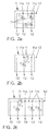
- FIGs 2a, 2b and 2c show three possible embodiments of the capacitance network 1, indicated hereinbelow as: network 1 ( Figure 2a ), network 2 ( Figure 2b ) and network 3 ( Figure 2c )
- the network 1 consists of three capacitors C1, C2 and C3, with C1 and C2 connected in series, and C3 in parallel with the series connection of C1 and C2.
- the network 2 consists of two capacitors C1 and C2 connected in series.
- the network 3 consists of four capacitors C1, C2, C3 and C4 connected as follows: C1 and C2 connected in series with each other, C3 and C4 connected in parallel with each other and also in parallel with the series connection of C1 and C2.
- the capacitors have a relation of known value; b) C1 has a value much greater than the other capacitors; c) the node or pin 12 connects the capacitance network 1 to the interface circuit 2; d) the remaining nodes or pins 12, according to the embodiment, connect the capacitance network 1 to the digital controller 3; and e) the comparison with the predefined voltage threshold can be performed at the three first nodes or pins 12 on the left (P1-P3), which allows, firstly, the detection to be performed at a low impedance point and thus a reduction of the capacitive interference effects and, secondly, the voltage threshold margin to be greater if a voltage drop instead of a voltage increase is detected.
- the interface circuit 2 and/or the capacitance network 1 and/or the controller 3 comprise at least one pin 12, 25, 33 for connections 13, 26, 34 and where the interface circuit 2 comprises at least one passive analog circuit 22 between the pin 12, 25 which connects said interface circuit 2 to the capacitance network 1 and at least one of the pins 25, 33 which connect said interface circuit 2 to the controller 3.
- the controller 3 will have four pins 33 for connection to the interface circuit 2 and/or to the capacitance network 1.
- At least one passive analog circuit 22 is composed of a plurality of passive electronic components 24.
- the interface circuit 2 comprises a Wheatstone bridge 23 in which at least one of the components 23a of each one of the arms is the analog sensor 21, said Wheatstone bridge 23 being connected to a plurality of passive electronic components 24.
- the interface circuit 2 is supplied via at least one of the input/output pins 33 of said controller 3.
- the controller 3 comprises a memory 31 with a plurality of codes 32 which correspond to the different ranges of values of the variable measured.
- the capacitance network 1 comprises at least one connection 13 which can be switched between at least two electrical capacitors 11 with known values.
- the relation of the capacitance between at least two of said electrical capacitors 11 is at least 100:1.
- the relation of the capacitance between at least two of said electrical capacitors 11 is at least 1,000:1.
- the relation of the capacitance between at least two of said electrical capacitors 11 is at least 10,000:1.
- said method consists in counting the number of cycles necessary for achieving a given voltage VT in a capacitance network 1 by redistributing (on successive occasions) a specific quantity of charge between its components; which charge is obtained by connecting one or more of these components, during a programmable time period, to a unknown voltage Vx which is generated by the interface circuit 2 which includes: 1) at least one analog sensor and 2) a passive interface circuit; both connected to the digital controller 3.
- Vx which includes: 1) at least one analog sensor and 2) a passive interface circuit; both connected to the digital controller 3.
- Said capacitance network 1 requires at least two capacitors 11 (or other component with capacitive properties), one of which must have a much greater capacitance than the others, and switchable connections.
- the number N of times that the charge redistribution process is repeated depends on the relation between the components of the capacitive network 1 and the voltage VT; consequently, in order to perform the switch-over of the analog sensor 21, it is sufficient to know the value of these parameters.
- the method may be implemented by means of a digital controller 3, without the need for any other active electronic component which is external or incorporated in its controller 3, such as an analog/digital converter or a circuit for measuring time by means of a clock signal and a voltage pulse counter.
- the variable measured is determined by means of comparison of the number N of times that the charge redistribution process is repeated with a series of digital codes corresponding to different value ranges of the variable measured, said digital codes being provided in the form of a table.
- Another way of determining the variable measured is to measure one or more passive reference components in order to produce the coefficients of a calibration curve and obtain the variable measured by means of calculation. Said table and the coefficients of the calibration curve are stored in the memory 31 of the digital controller 3 so that they can be used during the measurement process.
- the measurement method illustrated may be realized in different ways which involve a different number of components and interconnections in the capacitance network 1 and in the interface circuit 2.
- the method consists in at least three steps: a first step for zeroing any charge in the capacitance network 1; a second step for applying to the capacitance network 1 the voltage generated by the interface circuit 2 where the sensor 21 is located; and a third step for redistributing between one or more components of the capacitance network 1 the electrical charge applied during the previous step.
- the capacitance network is formed by at least two capacitances, one of which is much greater than the other ones. It should be pointed out, however, that the second step is not necessarily that for charging the smaller value of the capacitances, but one of these values.
- a voltage threshold may be detected on at least two different nodes or pins 12 of the capacitance network 1. Therefore, the voltage at the terminals of the capacitance of greatest value is not always measured.
- C1 is the greatest of the capacitances and is charged to the voltage between its terminals, which depends on the output voltage, the analog sensor 21 and/or the interface circuit 2 which includes it.
- the controller 3 limits the charging time of the at least one first electrical capacitor 11 of said capacitance network 1 so that said at least one first electrical capacitor 11 does not remain fully charged.
- the number N of repetitions of the charge redistribution process therefore depends on the relation between the capacitances of the two capacitors, the predefined threshold and the voltage of the circuit which incorporates the sensor 21.
- the charging time of the small capacitor may be limited so that it does not remain fully charged.
- Nx ln 1 - VT / VOH Rx R X + R R 1 - e - T R X + R R C 1 + C 3 R X + R R C 1 C 2 + C 3 + C 2 C 3 ln C 1 2 C 1 + C 2 C 1 + C 3
- VOH is the output voltage of the fourth pin on the left of the controller 3 during the charging step
- VT is the threshold voltage of the pin
- T is the time for which the fourth pin maintains the voltage VOH.
- the controller 3 counts the number of cycles necessary for achieving a given voltage at the terminals 11 a of said at least one second electrical capacitor 11, by redistributing on successive occasions a specific quantity of charge of the at least one first electrical capacitor 11 in said at least one second electrical capacitor 11.
- the controller 3 determines the measurement of the electrical variable of the analog sensor 21 by comparing the number of times which the charge redistribution is repeated, with a series of codes 32 stored previously in a memory 31 of said controller 3 and corresponding to different value ranges of the variable measured.
- the controller 3 determines the measurement of the electrical variable by comparing the number of times which the charge redistribution is repeated, with a series of codes 32 stored previously in a memory 31 of said controller 3 and corresponding to coefficients of a calibration curve of at least one passive electronic reference component 24.
- the interface circuit 2 comprises at least one analog sensor 21 and a passive reference component
- the controller 3 is a very low-cost, common, 8-bit microcontroller which does not incorporate any analog/digital converter or other analog or digital peripheral circuits
- the pins 33 are I/O (input/output) pins of the controller 3, the internal structure of these I/O (input/output) pins 33 allowing three logic states to be established: (a) output set to "0", with an output voltage V0; (b) output set to "1", with an output voltage V1; and (c) input or HZ, which may be enabled in order to interrupt the measurement process when a given voltage is reached;
- C1 and C2 are two electrical capacitors of known value, the relation of which is 10,000:1.
- the controller 3 performs a sequence of operations in order to measure the sensor 21 or a reference component.
- the controller 3 performs a sequence of operations in order to measure the sensor 21 or a reference component.
- the value of the measured variable may be determined.
- FIG 3 shows a first preferred embodiment of the apparatus according to Figure 1 , where the capacitance network 1 is the network 1 and the interface circuit 2 comprises a simple resistive sensor Rx and a resistance of R R of known value which are arranged in a resistive voltage divider.
- R1 and R2 are two reference resistances, known and stable, necessary for calculating the coefficients of a calibration curve and obtaining Rx by means of calculation.
- C3 is a capacitor of known value, the relation of which to C1 is 100,000: 1.
- the sequence of operations which the controller 3 performs to measure both Rx and R1 and R2 consists of three steps: (1) zeroing, (2) charging, and (3) redistribution and reading.
- the specific set of operations for measuring Rx is as follows: Initially seven first pins 33 (P1-P7) of the controller 3 are configured as HZ so as to avoid, upon start-up of the system, that these pins 33 are configured in an undesirable manner. Thereafter, in step (1), seven first pins 33 (P1-P7) are configured as an output set to "0"; therefore, any electric charge stored in the components of the interface circuit 3 is drained to earth.
- step (2) the third and fifth pin 33 (P3, P5) remain in their prior state, while the fourth pin 33 (P4) is configured as an output set to "1" and the first, second, third, sixth and seventh pins 33 (P1, P2, P3, P6 and P7) are configured as HZ; consequently, C2 starts to charge and if the fourth pin 33 (P4) remains in the state "1" (voltage V1) for a sufficiently long period of time with respect to the resultant time constant Tc of the circuit RC, it will finally reach the voltage Vx of the voltage divider formed by Rx and R R .
- the fourth pin 33 (P4) remains in the state "1" for a shorter period of time, the voltage at the terminals of C2 will be a fraction of Vx so that the charge stored in it will be less. It should be noted that, with this arrangement of pins, both C3 is charged to the voltage V2 which is on the second pin 33, and C1 is charged to the voltage difference V12 at its terminals.
- the first, third, sixth and seventh pins 33 (P1, P3, P6 and P7) remain in their prior state, the fourth and fifth pins 33 (P4 and P5) are configured as an input and the second pin 33 (P2) is configured as an output set "0".
- the charge stored in C2 is redistributed with C1, and the first pin 33 (P1) acts as a voltage comparator with TTL/CMOS threshold and high input impedance; the result is a voltage increase ⁇ VC1 at the terminals of C1 proportional to the redistributed charge, and therefore to Vx, which in turn depends on Rx.
- Steps (2) and (3) are repeated until the voltage between the terminals of C1 is equal to or greater than the threshold voltage VT at the first pin 33 (P1).
- the control program counts the charge cycles necessary for reaching said threshold, without the need for any timer or voltage pulse counter integrated in the controller 3. At the end of the sequence, a number Nx of charging cycles related to the change in impedance of the sensor 21 is obtained.
- Nx will be all the greater, and therefore the measurement resolution will be all the better, the shorter the time period during which the fourth pin 33 (P4) remain in the state "1 ".
- An alternative to the above sequence of operations is to detect the drop in voltage ⁇ VC3 at the terminals of C3 (on the second pin 33 (P2)), which depends on the charge which is stored in C1 during a previous measurement cycle. Thus, therefore, it is possible to detect a voltage threshold at at least two different nodes or pins 12 of the capacitance network 1.
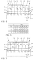
- Figure 4 is a table which summarises the logic state of the pins of the controller 3 during a cycle of the sequence for measuring Rx in the embodiment of Figure 3 .
- the sequence of operations which the controller 3 performs to measure R1 and R2 is similar to that which is performed to measure Rx; the difference is that the sixth and seventh pins (P6 and P7) carry out, for each measurement, the function which the fifth pin (P5) carried out before, while the pins 33 which are not involved in the measurement are configured as HZ.
- the value Ni of charging cycles arising for each resistance measured is N1 and N2.
- FIG. 5 shows a second preferred embodiment of the apparatus according to Figure 1 , where the capacitance network 1 is the network 3 and the interface circuit 2 comprises a simple capacitive sensor Cx and a resistance of R C of known value which are arranged in an RC circuit.
- C4 and C5 are two reference capacitors 11, the capacitances of which have a known and stable relation necessary for determining Cx.
- the sequence of operations which the controller 3 performs in order to measure both Cx and C4 and C5 consists of four steps: (1) zeroing, (2) charging, and (3) discharging/charging and reading, and (4) redistribution.
- the specific set of operations for measuring Cx is as follows: Initially, seven first pins 33 (P1-P7) are configured as HZ.
- step (1) seven first pins 33 (P1-P7) are configured as an output set to "0".
- step (2) P7 remains in its prior state, P6 is configured as an output set to "1", and P1 to P5 are configured as HZ; this arrangement of pins 33 is maintained for a sufficiently long time period compared to the time constant Tc of the circuit RC formed by Rc and Cx. Thus, therefore, Cx is charged via Rx to the voltage V1 of P6. It should be pointed out that this step of the measuring sequence is not to charge the capacitance network 1, but to apply a fixed change to the sensor 21.
- step (3) P1, P3, P4, P5 and P7 remain at HZ, and P2 and P6 are configured as an output set to "0" (voltage V0); consequently, Cx is discharged to V0 and the network 3 is charged to a fraction of the discharge voltage Vx at the terminals of Cx.
- the duration of this pin arrangement must be sufficiently short compared to Tc and determines the resolution which will be obtained during the measurement.
- the voltage level between the terminals of C2 will be detected and compared via P1.
- step (4) P2, P3, P4 and P4 remain in their prior state, P1 is configured as an output set to "0", and P6 and P7 are configured as HZ.
- the sequence of operations which the controller 3 performs to measure C3 and C4 is similar to that which is performed to measure Cx; the difference is that the pins 33 (P4 and P5) carry out, for each measurement, the function which the pin P7 carried out before, while the pins 33 which are not involved in the measurement are configured as HZ.
- the value Ni of charging cycles arising for each resistance measured is N3 and N4.
- FIG 7 shows a third preferred embodiment of the apparatus according to Figure 1 , where the capacitance network 1 is the network 1 and the interface circuit 2 comprises a simple inductive Lx sensor 21 and a known resistor RL, which are arranged in an RL circuit.
- L1 and L2 are two known and stable reference inductors necessary for determining Lx.
- the sequence of operations which the controller 3 performs to measure Lx, L1 and L2 is nearly the same as that which is used to measure Rx, R1 and R2, respectively, in the preferred embodiment of Figure 3 . It differs in that the time which is applied to charge C2 to Vx is now determined for the time constant of the network RL.
- Figure 8 shows a fourth preferred embodiment of the apparatus shown in Figure 1 , where the capacitance network 1 is the network 2 and the interface circuit 2 comprises a maximum of four sensors 21 based on a change of resistance (R3, R4, R5 and R6) and connected so as to form a Wheatstone bridge 23, and a resistance R P of known value.
- the pin P1 is used as a measurement node. Let us assume that all the sensors 21 undergo the same relative change in resistance x, which may be positive or negative.
- Figure 9 shows a fifth preferred embodiment of the apparatus shown in Figure 1 , where the capacitor network 1 is the network 2 and the interface circuit 2 comprises a photodiode D (sensor) and a known resistance R F , with a common node 25.
- the equivalent electric circuit of the photodiode allows analysis of the circuit formed by D and RF as an RC circuit, the time constant of which depends on the intensity of the electromagnetic radiation striking the photodiode.
- R7 and R8 are two known resistances which are used to control the time constant and thus improve the resolution during measurement.
- the sequence of operations which the controller 3 performs in order to measure the variation in impedance which D undergoes is similar to that which the controller 3 performs in order to measure Cx in the preferred embodiment of Figure 5 .
- the main differences are the pin arrangement 33 of the controller 3 and the time taken to charge C2 to Vx, which is now determined by the time constant of the circuit formed by D and R F .
- Figure 10 shows a table which summarises the logic state of the pins of the controller 3 during a cycle of the sequence for measuring D in the embodiment of Figure 9 , when D is reverse polarized via R F .
- the sequence of operations which the controller 3 performs to measure D when reverse polarization is performed via R7 and R8 is similar to that which is performed via R F ; the difference is that the pins P6 and P7 carry out, for each measurement, the function of the pin P4, while the pins 33 which are not involved in the measurement are configured as HZ.
- variable measured is determined by means of comparison of the number N of times that the charge redistribution process is repeated with a series of digital codes corresponding to different value ranges of the variable measured, said digital codes being provided in the form of a table in the control program of the controller 3.
Landscapes
- Physics & Mathematics (AREA)
- General Physics & Mathematics (AREA)
- Measurement Of Resistance Or Impedance (AREA)
Abstract
Description
- The subject of the present patent application is a device and method for measuring electrical variables of analog sensors according to
Claims - The present invention relates, in general, to systems for measuring analog sensors, including those which generate directly an electric current or voltage.
- The output signal of analog sensors is usually a low-amplitude electrical voltage generated by the sensor or by an interface circuit which incorporates one or more sensors and, if necessary, one or more electric voltage or current sources. The methods proposed according to the present state of the art for measuring said output voltage or current of analog sensors or of its interface circuits are numerous and at present all strive to obtain a digital output which may be achieved directly or indirectly.
- Obtaining directly a digital output from the voltage generated by the sensor, or by the interface circuit to which the sensor is connected in order to obtain an analog output voltage, is achieved by means of an analog-to-digital voltage converter (A/D converter or ADC), which may be a specific integrated circuit, or a circuit embedded in another multifunctional circuit, such as a digital controller. The output of said analog/digital converter is processed digitally in order to extract the desired information or in order to take a decision. In order to adapt the output signal of the sensor or of its interface circuit to the range of input amplitudes of the A/D converter, a signal conditioning circuit which includes at least one component capable of amplifying voltages or currents is added.
- The interface circuits for resistive sensors are usually based on voltage dividers, for example when the change in resistance relative to its initial value is great, or on circuits derived from the voltage divider, for example when the change in resistance relative to its initial value is small. Wheatstone bridges and continuous pseudo-bridges, such as those described, for example, in the patent
US3130578 and in the patent applicationsEP1397654 andUS20130249574 may be regarded as interface circuits derived from the voltage divider. - The interface circuits for capacitive or inductive sensors may also be based on voltage dividers, or may consist of bridges supplied by an alternating voltage, or resonant circuits, such as those described for example in the patent
US2932970 and in the patent applicationUS20130271158 . The resistive sensors may also be incorporated in resonant circuits. - The analog sensors based on a variation in resistance, capacitance or inductance may be of the simple or differential type. In the first case they take the form of a single electronic component which changes with the variable measured, whereas in the second case they take the form of two electronic components which have a common node and in which the variable measured causes a change of the same magnitude, but in the opposite direction.
- In general, voltage dividers may include a simple sensor or a differential sensor, while (continuous or alternating) bridges may include one, two, three or four variable impedance sensors or various sensors which are connected in combinations in series and in parallel and which are arranged in one, two or three arms of the bridge. Voltage dividers have as a minimum three terminals for connection with the signal conditioning circuit which requires the A/D converter: an excitation voltage is applied between two terminals and the voltage is measured between the third terminal and one of the two prior terminals. Sensor bridges, instead, have a minimum of four terminals which are usually connected in pairs: via one pair the bridge is excited by means of a electric voltage or current, and via the other pair the output voltage or current is detected.
- Thus, the conventional method for measuring analog sensors directly is to arrange them in a circuit which obtains an electric voltage related to the variable detected by the sensor and to digitalize said voltage with an analog/digital converter (ADC).
- Alternatively, the sensors based on a variation in resistance or capacitance may be placed in a circuit which generates a signal, the duration of which depends on the value of the magnitude detected by the sensor. In order to obtain a digital output it is sufficient to measure therefore the duration of that signal for which a clock signal is required, it being then a more economical process than an analog/digital converter (ADC).
- The manufacturers of automotive components offer integrated solutions for measuring physical and chemical parameters which include a sensor element and the electronic circuits necessary for offering a standardized electrical output (e.g. for a CAN bus). If the electrical output is not normalized, the sensor is connected to an associated control unit (ECUs, switch-boards) which usually accept various sensors. An example would be the electronic circuits which must be connected to a sensor element in order to measure the angle of the steering wheel. However, there exist at present in a motor vehicle many other sensors which could benefit from the development of the invention. Some of these could be:
- 1. Position and rotational angle sensors These are based on the change in electrical resistance of an angular or linear potentiometer and on the change in electrical resistance of a magneto-resistance. They are used to measure for example: the position of the accelerator pedal, the travel and position of the suspension, the position of the butterfly valves, and the position of the sensor plate in the injection system.
In the following patents it can be understood that many manufacturers continue proposing solutions based on the conventional structure involving conditioning and digitalization of the signal obtained by the sensor element: "US844125282 . Rotational angle measurement apparatus", "DE102006032266A1 . Sensor component", "DE60218016D1 . Electrically assisted steering" and "DE102009032664A1 . Motor vehicle accelerator pedal". - 2. Absolute and differential pressure sensors These are based on changes in electric resistance due to a mechanical deformation. They are used to measure the pressure of: fuel, brake liquid, oil and coolant.
- In the case of these sensors also, in the patents of various manufacturers the latter continue to proposes solutions based on the conventional measuring structure described above.
- Furthermore, and depending on the desired precision and resolution, the signal conditioning circuits prior to the A/D converter and connected to the sensor interface circuit may require: voltage transformers: active components, such as operational or instrumentation amplifiers, and voltage comparators; complex manual or automatic adjustment systems.
- These components and methods increase the cost of the final product up to a value which may be excessive for given applications or application areas.
- In short, an analysis of the information existing hitherto shows that the current methods for measuring analog sensors are subject to some of the following drawbacks: (a) the need for an analog/digital converter and the (active) conditioning circuit in order to adapt the output voltage of the interface circuit or the sensor to the range of input amplitudes of the analog/digital converter; (b) the need for a digital counter and a clock signal, the frequency of which determines the resolution which will be obtained during measurement; and (c) the applicability limited to a type of sensor, for example for the transfer of charge to the capacitive sensors.
- Thus there still exists the need for a device, and an associated method, for measuring analog sensors based on a change in capacitance, electrical resistance or inductance or which generate directly an electric current or voltage of the order of millivolts. This includes numerous sensors for temperature, lighting, position, proximity, displacement, force, pressure and other variables usually found in the automotive sector and in other industrial sectors.
- In accordance with the present invention, this task is solved by means of a device and method for measuring electrical variables of analog sensors according to
Claims - The object of the present patent application is to provide a new method for measuring analog sensors which are based on a change in electrical resistance (resistive sensors), capacitance (capacitive sensors) or inductance (inductive sensors) or which generate directly an electric current or voltage (generators). A second object is to provide a device, based on said measurement method, using for this purpose: a network of capacitors of known value and switchable connections; a circuit which includes: at least one analog sensor and a passive interface circuit; and a digital controller.
- The innovative solution proposed consists in that the object of the present invention may be achieved by using at least two electrical capacitors and a controller, without the need for any other active electronic component, apart from said controller.
- Thus, and more specifically, the device for measuring electrical variables of analog sensors comprises a controller, preferably a digital controller, connected to a capacitance network and an interface circuit connected to an analog sensor, wherein said capacitance network: is connected to said interface circuit connected to the analog sensor, comprises at least two electrical capacitors of known value (or any other element with capacitive properties), wherein the relation of the capacitance between at least two of said electrical capacitors is at least 10:1.
- In this way the connection of the interface circuit to the digital controller avoids the need for an external power supply source and enables the current required to charge at least a first electrical capacitor of the capacitance network to be obtained. On the other hand the interface circuit which is proposed uses fewer electronic component than the sensors currently available, with connection of the sensor element directly to the microcontroller, without the need for intermediate integrated circuits for processing and digitalization of the signal provided by the sensor element. Only a number of passive components (resistors, electrical capacitors, etc.) are required. This absence of active components and the smaller number of passive components needed result in a lower cost and a greater reliability.
- According to another aspect of the invention, the interface circuit and/or the capacitance network and/or the controller comprise at least one connection pin, wherein the interface circuit comprises at least one passive analog circuit between the pin which connects said interface circuit with the capacitance network and at least one of the pins which connect said interface circuit to the controller. "Passive analog circuit" is understood as meaning a purely resistive circuit, in the manner of a voltage divider, but it may also be an RC, RL or R circuit in parallel with a photodiode. The sensor and the calibration components are in parallel with a resistor.
- As a result, the at least one passive analog circuit is composed of a plurality of passive electronic components, whereby these may be resistive, capacitive or inductive components; or a combination of these, RC or RL, including optionally photodiodes. In this way different alternatives for implementing the circuit are provided, such as the possibility of carrying out the measurement of sensors with a different main electrical property, be it resistive, capacitive or inductive. Also it allows the measurement of light strengths and levels using a photodiode.
- In an alternative embodiment of the invention, the interface circuit comprises a Wheatstone bridge in which at least one of the components of each one of the arms is the analog sensor, said Wheatstone bridge being connected to a plurality of passive electronic components. In this way an alternative configuration to the series/parallel arrangement of electrical components is provided, and the advantages of the Wheatstone bridge arrangement are exploited.
- According to the operating principle of the device, the interface circuit is supplied via at least one of the input/output pins of said controller. In this way an additional and independent power supply source is not necessary and instead the outputs of the associated controller are used.
- According to another aspect of the invention, the controller, which is preferably digital, comprises a memory with a plurality of codes which correspond to the different ranges of values of the variable measured. In this way measurement ranges are established and, by means of comparison, it is determined within which of them the measurement performed lies, thus defining the corresponding output information of the controller in a predetermined format and/or values.
- On the other hand, the capacitance network comprises at least one connection switchable between at least two electrical capacitors with known values. It is thus possible to eliminate optionally from the circuit concrete components, by bridging them or else disconnecting them from the circuit leaving at least one of its terminals freely exposed.
- It should be mentioned that, in a preferred embodiment of the invention, the relation of the capacitance between at least two of said electrical capacitors is at least 100:1. In this way it is possible to establish greater precision in the measurement since a greater number of charge redistribution cycles for the same measurement are required.
- In another preferred embodiment of the invention, the relation of the capacitance between at least two of said electrical capacitors is at least 1,000:1. In this way it is possible to establish even greater precision in the measurement since a greater number of charge redistribution cycles are required for the same measurement.
- In yet another preferred embodiment of the invention, the relation of the capacitance between at least two of said electrical capacitors is at least 10,000:1. In this way it is possible to establish an even greater precision in the measurement since a greater number of charge redistribution cycles are required for the same measurement.
- It is also an object of the present patent application to provide a method for measuring electrical variables of analog sensors, which comprises the following steps:
- a) generating a voltage by means of the analog sensor and/or the interface circuit which includes it;
- b) charging with said voltage at least one first electrical capacitor of said capacitance network, by switching the connections between the controller, the capacitance network and the analog signal and/or the interface circuit.
- c) redistributing the charge stored in said at least one first electrical capacitor in at least one second electrical capacitor of said capacitance network, by switching the connections between the controller and the capacitance network;
- d) repeating the steps a), b) and c) until the voltage at the terminals of the at least one second electrical capacitor of the capacitance network reaches a predefined voltage threshold.
- Said method does not require either an analog/digital converter (ADC), nor any time measurement device, but a simple event counter. It is based on the use of a capacitance network which comprises at least two electrical capacitors with known values, one of which is much greater than the other one. In order to measure the voltage generated by the circuit which incorporates the sensor, at least one of the two capacitors is charged with said voltage and the charge is then redistributed in them. The process is repeated until the voltage at the terminals of at least one of the capacitors reaches a predefined voltage threshold VT. The number N of repetitions of the charge redistribution process therefore depends on the relation between the capacitances of the two capacitors, the predefined threshold and the voltage of the circuit which incorporates the sensor. In order to increase the value of N and thus improve the resolution of the method, the charging time of the small capacitor may be limited so that said capacitor does not remain fully charged.
- All the functions of switching the connections between capacitors, comparison with a voltage threshold, control of the charging time and counting of events may be performed using a simple low-cost microcontroller which provides a standard digital output.
- Indirectly obtaining a digital output from the changes which the sensor undergoes depending on the variable detected consists in deducing the value of this variable using a model (e.g. a formula) which relates its value to that of another variable of a different kind, but which is not an electrical voltage or current and which is related to that variable of interest. This method is capable, therefore, of obtaining a digital output without the need for voltage digitalizing devices, namely, without an A/D converter.
- The transfer of charge from one unknown capacitor (sensor) to another capacitor of known value is a habitual process for measuring capacitive sensors which are charged to a known voltage. The method described in this patent is different because: (a) it requires a capacitance network which comprises at least two capacitors of known value (or any other component with capacitive properties) such that the relation between its capacitances is known, while in the known charge transfer methods the capacitance of an unknown capacitor is determined; (b) the voltage Vx needed to charge the components of the capacitance network is not a known voltage (as in the known charge transfer methods) but it is generated by the sensor or by a circuit where the sensor is connected to passive components; and (c) the voltage which, when it reaches the value VT, causes termination of the process is not the voltage at the terminals of a specific capacitor, but it is obtained at the terminals of at least two capacitors of the capacitance network which depends on the structure of this network. As a result of these differences it is possible to obtain at least four advantages which are lacking in the known charge transfer methods used hitherto to measure capacitive sensors. (1) the method may be applied both to capacitive sensors, as well as to resistive sensors, inductive sensors or voltage or current generating sensors; (2) the resolution may be improved by controlling the time during which the voltage Vx is applied to one or more components of the capacitance network; (3) the resolution may be improved also by detecting the drop in voltage instead of the voltage increase, for example at the terminals of a capacitor; and (4) the detection of voltage at the terminals of at least two capacitors of the capacitance network may be performed at a low earth impedance node and thus reduce the effects of capacitive interferences.
- Advantageously, the controller limits the charging time of the at least one first electrical capacitor of said capacitance network so that said at least one first electrical capacitor does not remain fully charged. In this way (limiting for example the charging time of the small capacitor) the value of N increases and thus improves the resolution of the method.
- The operating principle of the method is based on the fact that the controller counts the number of cycles necessary for achieving a given voltage at the terminals of said at least one second electrical capacitor, by redistributing on successive occasions a specific quantity of charge of the at least one first electrical capacitor in said at least one second electrical capacitor. In this way it is possible to perform a measurement in such a simple way as that of counting a number of charging and discharging cycles.
- According to another aspect of the invention the controller determines the measurement of the electrical variable of the analog sensor by comparing the number of times which the charge redistribution is repeated with a series of codes stored previously in a memory of said controller and corresponding to different ranges of values of the variable measured. In this way measurement ranges are established and, by means of comparison, it is determined within which of them the measurement performed lies, thus defining the corresponding output information of the controller in a predetermined format and/or values.
- According to yet another aspect of the invention, the controller determines the measurement of the electrical variable by comparing the number of times which the charge redistribution is repeated with a series of codes stored previously in a memory of said controller and corresponding to a number of coefficients of a calibration curve of at least one passive electronic reference component. In this way, and by means of a simple calculation, the variable measured during processing of the measurement is obtained.
- The attached drawings illustrate, by way of a non-limiting example, a device for measuring electrical variables of analog sensors, provided in accordance with the invention. Other characteristic features and advantages of said device and the associated method for measuring electrical variables of analog sensors, forming the subject of the present invention, will become clear from the description of a preferred, but not exclusive embodiment which is illustrated by way of a non-limiting example in the accompanying drawings in which:
-
-
Figure 1 shows a block diagram of the device proposed, in accordance with the present invention; -
Figure 2a shows a first possible embodiment of the capacitance network, in accordance with the present invention; -
Figure 2b shows a second possible embodiment of the capacitance network, in accordance with the present invention; -
Figure 2c shows a third possible embodiment of the capacitance network, in accordance with the present invention; -
Figure 3 shows a preferred embodiment of the apparatus proposed inFigure 1 , where the interface circuit comprises a simple resistive sensor Rx connected to other passive components, in accordance with the present invention; -
Figure 4 shows a table which summarises the logic state of the pins of the controller during the sequence of operations for measuring Rx in the preferred embodiment ofFigure 3 , in accordance with the present invention; -
Figure 5 shows a preferred embodiment of the device proposed inFigure 1 , where the interface circuit comprises a simple capacitive sensor Cx connected to other passive components, in accordance with the present invention; -
Figure 6 shows a table which summarises the logic state of the pins of the controller during the sequence of operations for measuring Cx in the preferred embodiment ofFigure 5 , in accordance with the present invention; -
Figure 7 shows a preferred embodiment of the apparatus proposed inFigure 1 , wherein the interface circuit comprises a simple inductive sensor Lx connected to other passive components, in accordance with the present invention; -
Figure 8 shows a preferred embodiment of the apparatus proposed inFigure 1 , wherein the interface circuit comprises four simple resistive sensors (R3, R4, R5 and R6) connected to form a Wheatstone bridge 23, in accordance with the present invention; -
Figure 9 shows a preferred embodiment of the apparatus proposed inFigure 1 , wherein the interface circuit comprises a photodiode (sensor) D connected to other passive components, in accordance with the present invention; -
Figure 10 shows a table which summarises the logic state of the pins of the controller during the sequence of operations for measuring D in the preferred embodiment ofFigure 9 . - In the light of the aforementioned figures and in accordance with the numbering adopted, said figures show a preferred example of embodiment of the invention which comprises the parts and elements which are indicated and described in detail below.
- Thus, as can be seen in
Figures 1 and3 , the device for measuring electrical variables of analog sensors which comprises acontroller 3 connected to acapacitance network 1 and to aninterface circuit 2 connected to ananalog sensor 21, characterized in that said capacitance network 1: is connected to saidinterface circuit 2 connected to theanalog sensor 21, comprises at least twoelectrical capacitors 11 of known value, wherein the relation of the capacitance between at least two of saidelectrical capacitors 11 is at least 10:1. - More specifically, the device conceived is based on a
digital controller 3 which has, connected thereto, acapacitance network 1 and aninterface circuit 2 which includes at least oneanalog sensor 21 connected, in each case, topassive components 24.Figure 1 is a block diagram of the measurement device proposed, where thecapacitance network 1 comprises at least twocapacitors 11 with known values (one of which much greater than the other ones) andswitchable connections 13; thedigital controller 3 has a finite number (m) of input/output pins (I/O) (P1,P2, ... Pn, Pn+1, Pn+2, ..., Pm) to which various nodes of thecapacitance network 1 and theinterface circuit 2 are connected. By means of the internal structure of the circuit connected to these I/O pins, three logic states may be determined: (a) output set to "0"; (b) output set to "1"; and (c) high input impedance state or input (HZ) which is the state adapted to the variable which is to be detected (voltage) and which may be enabled so that the measurement process is interrupted when a given voltage level is reached. The I/O voltage levels on each of these pins depends on the microelectronic technology used to manufacture thedigital controller 3. Each one of these logic states is necessary in order for thedigital controller 3 to perform a number of connection functions in thecapacitance network 1 and theinterface circuit 2, control of the charging time, counting of the charging cycles, and a comparison with a voltage threshold; all of this without the need for time or voltage measurement circuits incorporated in thedigital controller 3 or outside of saiddigital controller 3. Thedigital controller 3 may be used moreover for other functions such as storage, display or communication of the measurement readings, combined or separately, with independence of the sensor or the component being measured. -
Figures 2a, 2b and 2c show three possible embodiments of thecapacitance network 1, indicated hereinbelow as: network 1 (Figure 2a ), network 2 (Figure 2b ) and network 3 (Figure 2c ) Thenetwork 1 consists of three capacitors C1, C2 and C3, with C1 and C2 connected in series, and C3 in parallel with the series connection of C1 and C2. Thenetwork 2 consists of two capacitors C1 and C2 connected in series. Thenetwork 3 consists of four capacitors C1, C2, C3 and C4 connected as follows: C1 and C2 connected in series with each other, C3 and C4 connected in parallel with each other and also in parallel with the series connection of C1 and C2. In each one of these embodiments: a) the capacitors have a relation of known value; b) C1 has a value much greater than the other capacitors; c) the node orpin 12 connects thecapacitance network 1 to theinterface circuit 2; d) the remaining nodes or pins 12, according to the embodiment, connect thecapacitance network 1 to thedigital controller 3; and e) the comparison with the predefined voltage threshold can be performed at the three first nodes or pins 12 on the left (P1-P3), which allows, firstly, the detection to be performed at a low impedance point and thus a reduction of the capacitive interference effects and, secondly, the voltage threshold margin to be greater if a voltage drop instead of a voltage increase is detected. These embodiments are simple examples for facilitating understanding of the patent of invention, but are not exhaustive as regards the detail of the circuits. - Additionally, as can be seen in
Figures 3 ,5 ,7 and9 , theinterface circuit 2 and/or thecapacitance network 1 and/or thecontroller 3 comprise at least onepin connections interface circuit 2 comprises at least onepassive analog circuit 22 between thepin interface circuit 2 to thecapacitance network 1 and at least one of thepins interface circuit 2 to thecontroller 3. In a preferred embodiment of the invention, thecontroller 3 will have fourpins 33 for connection to theinterface circuit 2 and/or to thecapacitance network 1. - It should be mentioned, as can be seen in
Figures 3 ,5 ,7 and9 , that at least onepassive analog circuit 22 is composed of a plurality of passiveelectronic components 24. - On the other hand, as can be seen in
Figure 8 , theinterface circuit 2 comprises a Wheatstone bridge 23 in which at least one of thecomponents 23a of each one of the arms is theanalog sensor 21, said Wheatstone bridge 23 being connected to a plurality of passiveelectronic components 24. - According to another aspect of the invention, as can be seen in
Figures 1 ,3 ,5, 7 and9 , theinterface circuit 2 is supplied via at least one of the input/output pins 33 of saidcontroller 3. - According to a preferred embodiment of the invention, as can be seen in
Figures 1 ,3 ,5, 7 and9 , thecontroller 3 comprises amemory 31 with a plurality of codes 32 which correspond to the different ranges of values of the variable measured. - More particularly, as can be seen in
Figures 2a, 2b and 2c , thecapacitance network 1 comprises at least oneconnection 13 which can be switched between at least twoelectrical capacitors 11 with known values. - According to a preferred embodiment of the invention, the relation of the capacitance between at least two of said
electrical capacitors 11 is at least 100:1. - According to another preferred embodiment of the invention, the relation of the capacitance between at least two of said
electrical capacitors 11 is at least 1,000:1. - According to yet another preferred embodiment of the invention, the relation of the capacitance between at least two of said
electrical capacitors 11 is at least 10,000:1. - It is also an object of the present patent application to provide a method for measuring electrical variables of
analog sensors 21, which comprises the following steps: - a) generating a voltage by means of the
analog sensor 21 and/or theinterface circuit 2 which includes it; - b) charging with said voltage at least one first
electrical capacitor 11 of saidcapacitance network 1, by switching the connections between thecontroller 3, thecapacitance network 1 and theanalog signal 21 and/or theinterface circuit 2. - c) redistributing the charge stored in said at least one first
electrical capacitor 11 in at least one secondelectrical capacitor 11 of saidcapacitance network 1, by switching the connections between thecontroller 3 and thecapacitance network 1; - d) repeating the steps a), b) and c) until the voltage at the
terminals 11a of the at least one secondelectrical capacitor 11 of thecapacitance network 1 reaches a predefined voltage threshold. - Thus, said method consists in counting the number of cycles necessary for achieving a given voltage VT in a
capacitance network 1 by redistributing (on successive occasions) a specific quantity of charge between its components; which charge is obtained by connecting one or more of these components, during a programmable time period, to a unknown voltage Vx which is generated by theinterface circuit 2 which includes: 1) at least one analog sensor and 2) a passive interface circuit; both connected to thedigital controller 3. The shorter said connection of Vx to thecapacitance network 1, the less will be the charge stored in the components of said network, and the greater will be the number of times that the process will have to be repeated, thereby improving the resolution of the measurement. Saidcapacitance network 1 requires at least two capacitors 11 (or other component with capacitive properties), one of which must have a much greater capacitance than the others, and switchable connections. The number N of times that the charge redistribution process is repeated depends on the relation between the components of thecapacitive network 1 and the voltage VT; consequently, in order to perform the switch-over of theanalog sensor 21, it is sufficient to know the value of these parameters. The method may be implemented by means of adigital controller 3, without the need for any other active electronic component which is external or incorporated in itscontroller 3, such as an analog/digital converter or a circuit for measuring time by means of a clock signal and a voltage pulse counter. - The variable measured is determined by means of comparison of the number N of times that the charge redistribution process is repeated with a series of digital codes corresponding to different value ranges of the variable measured, said digital codes being provided in the form of a table. Another way of determining the variable measured is to measure one or more passive reference components in order to produce the coefficients of a calibration curve and obtain the variable measured by means of calculation. Said table and the coefficients of the calibration curve are stored in the
memory 31 of thedigital controller 3 so that they can be used during the measurement process. - The measurement method illustrated may be realized in different ways which involve a different number of components and interconnections in the
capacitance network 1 and in theinterface circuit 2. Whatever the form and the sequence of operations which thedigital controller 3 performs, the method consists in at least three steps: a first step for zeroing any charge in thecapacitance network 1; a second step for applying to thecapacitance network 1 the voltage generated by theinterface circuit 2 where thesensor 21 is located; and a third step for redistributing between one or more components of thecapacitance network 1 the electrical charge applied during the previous step. Some of these sequences of operations are described at the end of the description, in the preferred embodiments of the measurement apparatus proposed. - It should be mentioned that the capacitance network is formed by at least two capacitances, one of which is much greater than the other ones. It should be pointed out, however, that the second step is not necessarily that for charging the smaller value of the capacitances, but one of these values. A voltage threshold may be detected on at least two different nodes or pins 12 of the
capacitance network 1. Therefore, the voltage at the terminals of the capacitance of greatest value is not always measured. - By way of example, in
Figure 2b , C1 is the greatest of the capacitances and is charged to the voltage between its terminals, which depends on the output voltage, theanalog sensor 21 and/or theinterface circuit 2 which includes it. - According to another aspect of the invention, the
controller 3 limits the charging time of the at least one firstelectrical capacitor 11 of saidcapacitance network 1 so that said at least one firstelectrical capacitor 11 does not remain fully charged. - Thus the number N of repetitions of the charge redistribution process therefore depends on the relation between the capacitances of the two capacitors, the predefined threshold and the voltage of the circuit which incorporates the
sensor 21. In order to increase the value of N and thus improve the resolution of the method, the charging time of the small capacitor may be limited so that it does not remain fully charged. - Below an example of a mathematical formula of said relation is provided, although there is no one single mathematical formula specifically designed for each one of the preferred embodiments proposed. Each equation depends on the components which form the interface circuit and the
sensor 21. The equation which is shown is applicable for obtaining Nx in the circuit according toFigure 3 .
controller 3 during the charging step, VT is the threshold voltage of the pin and T is the time for which the fourth pin maintains the voltage VOH. - More specifically, the
controller 3 counts the number of cycles necessary for achieving a given voltage at theterminals 11 a of said at least one secondelectrical capacitor 11, by redistributing on successive occasions a specific quantity of charge of the at least one firstelectrical capacitor 11 in said at least one secondelectrical capacitor 11. - According to another aspect of the invention the
controller 3 determines the measurement of the electrical variable of theanalog sensor 21 by comparing the number of times which the charge redistribution is repeated, with a series of codes 32 stored previously in amemory 31 of saidcontroller 3 and corresponding to different value ranges of the variable measured. - According to another aspect of the invention the
controller 3 determines the measurement of the electrical variable by comparing the number of times which the charge redistribution is repeated, with a series of codes 32 stored previously in amemory 31 of saidcontroller 3 and corresponding to coefficients of a calibration curve of at least one passiveelectronic reference component 24. - Below five preferred embodiments of the invention are described where: (a) the
interface circuit 2 comprises at least oneanalog sensor 21 and a passive reference component; (b) thecontroller 3 is a very low-cost, common, 8-bit microcontroller which does not incorporate any analog/digital converter or other analog or digital peripheral circuits; (c) thepins 33 are I/O (input/output) pins of thecontroller 3, the internal structure of these I/O (input/output) pins 33 allowing three logic states to be established: (a) output set to "0", with an output voltage V0; (b) output set to "1", with an output voltage V1; and (c) input or HZ, which may be enabled in order to interrupt the measurement process when a given voltage is reached; (d) C1 and C2 are two electrical capacitors of known value, the relation of which is 10,000:1. In each one of these embodiments thecontroller 3 performs a sequence of operations in order to measure thesensor 21 or a reference component. Thus, therefore, there exist a number Ni of charging cycles for thesensor 21 or the measured reference component. Whence, using the equation which for eachinterface circuit 2 relates Vx to the value of thesensor 21, the value of the measured variable may be determined. -
Figure 3 shows a first preferred embodiment of the apparatus according toFigure 1 , where thecapacitance network 1 is thenetwork 1 and theinterface circuit 2 comprises a simple resistive sensor Rx and a resistance of RR of known value which are arranged in a resistive voltage divider. R1 and R2 are two reference resistances, known and stable, necessary for calculating the coefficients of a calibration curve and obtaining Rx by means of calculation. C3 is a capacitor of known value, the relation of which to C1 is 100,000: 1. The sequence of operations which thecontroller 3 performs to measure both Rx and R1 and R2 consists of three steps: (1) zeroing, (2) charging, and (3) redistribution and reading. The specific set of operations for measuring Rx is as follows: Initially seven first pins 33 (P1-P7) of thecontroller 3 are configured as HZ so as to avoid, upon start-up of the system, that thesepins 33 are configured in an undesirable manner. Thereafter, in step (1), seven first pins 33 (P1-P7) are configured as an output set to "0"; therefore, any electric charge stored in the components of theinterface circuit 3 is drained to earth. Then, in step (2), the third and fifth pin 33 (P3, P5) remain in their prior state, while the fourth pin 33 (P4) is configured as an output set to "1" and the first, second, third, sixth and seventh pins 33 (P1, P2, P3, P6 and P7) are configured as HZ; consequently, C2 starts to charge and if the fourth pin 33 (P4) remains in the state "1" (voltage V1) for a sufficiently long period of time with respect to the resultant time constant Tc of the circuit RC, it will finally reach the voltage Vx of the voltage divider formed by Rx and RR. If instead the fourth pin 33 (P4) remains in the state "1" for a shorter period of time, the voltage at the terminals of C2 will be a fraction of Vx so that the charge stored in it will be less. It should be noted that, with this arrangement of pins, both C3 is charged to the voltage V2 which is on thesecond pin 33, and C1 is charged to the voltage difference V12 at its terminals. Finally, in step (3), the first, third, sixth and seventh pins 33 (P1, P3, P6 and P7) remain in their prior state, the fourth and fifth pins 33 (P4 and P5) are configured as an input and the second pin 33 (P2) is configured as an output set "0". With this new arrangement of thepins 33, the charge stored in C2 is redistributed with C1, and the first pin 33 (P1) acts as a voltage comparator with TTL/CMOS threshold and high input impedance; the result is a voltage increase ΔVC1 at the terminals of C1 proportional to the redistributed charge, and therefore to Vx, which in turn depends on Rx. Steps (2) and (3) are repeated until the voltage between the terminals of C1 is equal to or greater than the threshold voltage VT at the first pin 33 (P1). The control program counts the charge cycles necessary for reaching said threshold, without the need for any timer or voltage pulse counter integrated in thecontroller 3. At the end of the sequence, a number Nx of charging cycles related to the change in impedance of thesensor 21 is obtained. Nx will be all the greater, and therefore the measurement resolution will be all the better, the shorter the time period during which the fourth pin 33 (P4) remain in the state "1 ". An alternative to the above sequence of operations is to detect the drop in voltage ΔVC3 at the terminals of C3 (on the second pin 33 (P2)), which depends on the charge which is stored in C1 during a previous measurement cycle. Thus, therefore, it is possible to detect a voltage threshold at at least two different nodes or pins 12 of thecapacitance network 1. -
Figure 4 is a table which summarises the logic state of the pins of thecontroller 3 during a cycle of the sequence for measuring Rx in the embodiment ofFigure 3 . The sequence of operations which thecontroller 3 performs to measure R1 and R2 is similar to that which is performed to measure Rx; the difference is that the sixth and seventh pins (P6 and P7) carry out, for each measurement, the function which the fifth pin (P5) carried out before, while thepins 33 which are not involved in the measurement are configured as HZ. Thus, therefore, the value Ni of charging cycles arising for each resistance measured is N1 and N2. Whence, using the equation which relates the voltage Vx of theinterface circuit 2 to the value of Rx, it is possible to determine Rx with independence of VT and RR. The changes in these components and parameters should not affect the measurement, instead the latter will depend on R1 ad R2 which must be sufficiently stable. -
Figure 5 shows a second preferred embodiment of the apparatus according toFigure 1 , where thecapacitance network 1 is thenetwork 3 and theinterface circuit 2 comprises a simple capacitive sensor Cx and a resistance of RC of known value which are arranged in an RC circuit. C4 and C5 are tworeference capacitors 11, the capacitances of which have a known and stable relation necessary for determining Cx. The sequence of operations which thecontroller 3 performs in order to measure both Cx and C4 and C5 consists of four steps: (1) zeroing, (2) charging, and (3) discharging/charging and reading, and (4) redistribution. The specific set of operations for measuring Cx is as follows: Initially, seven first pins 33 (P1-P7) are configured as HZ. Then, in step (1), seven first pins 33 (P1-P7) are configured as an output set to "0". Then, in step (2), P7 remains in its prior state, P6 is configured as an output set to "1", and P1 to P5 are configured as HZ; this arrangement ofpins 33 is maintained for a sufficiently long time period compared to the time constant Tc of the circuit RC formed by Rc and Cx. Thus, therefore, Cx is charged via Rx to the voltage V1 of P6. It should be pointed out that this step of the measuring sequence is not to charge thecapacitance network 1, but to apply a fixed change to thesensor 21. Thereafter, in step (3), P1, P3, P4, P5 and P7 remain at HZ, and P2 and P6 are configured as an output set to "0" (voltage V0); consequently, Cx is discharged to V0 and thenetwork 3 is charged to a fraction of the discharge voltage Vx at the terminals of Cx. The duration of this pin arrangement must be sufficiently short compared to Tc and determines the resolution which will be obtained during the measurement. During this same step, the voltage level between the terminals of C2 will be detected and compared via P1. Finally, in step (4), P2, P3, P4 and P4 remain in their prior state, P1 is configured as an output set to "0", and P6 and P7 are configured as HZ. The steps (2), (3) and (4) are repeated until the voltage between the terminals of C2 is equal to or greater than the threshold voltage VT P1. At the end of the sequence, a number Nx of charging cycles related to the change in impedance of thesensor 21 is obtained. It should be noted that the voltage VT is achieved between the terminals of C2 during the discharging/charging step (3). However, it could also be achieved between the terminals C1 during the redistribution step (4).Figure 6 shows a table which summarises the logic state of the pins of thecontroller 3 during a cycle of the sequence of operations for measuring Cx in the embodiment inFigure 5 . - The sequence of operations which the
controller 3 performs to measure C3 and C4 is similar to that which is performed to measure Cx; the difference is that the pins 33 (P4 and P5) carry out, for each measurement, the function which the pin P7 carried out before, while thepins 33 which are not involved in the measurement are configured as HZ. Thus, therefore, the value Ni of charging cycles arising for each resistance measured is N3 and N4. Whence, using the equation which relates the voltage Vx of theinterface circuit 2 to Cx, it is possible to determine Cx with independence of VT and Rc. -
Figure 7 shows a third preferred embodiment of the apparatus according toFigure 1 , where thecapacitance network 1 is thenetwork 1 and theinterface circuit 2 comprises a simpleinductive Lx sensor 21 and a known resistor RL, which are arranged in an RL circuit. L1 and L2 are two known and stable reference inductors necessary for determining Lx. The sequence of operations which thecontroller 3 performs to measure Lx, L1 and L2 is nearly the same as that which is used to measure Rx, R1 and R2, respectively, in the preferred embodiment ofFigure 3 . It differs in that the time which is applied to charge C2 to Vx is now determined for the time constant of the network RL. -
Figure 8 shows a fourth preferred embodiment of the apparatus shown inFigure 1 , where thecapacitance network 1 is thenetwork 2 and theinterface circuit 2 comprises a maximum of foursensors 21 based on a change of resistance (R3, R4, R5 and R6) and connected so as to form a Wheatstone bridge 23, and a resistance RP of known value. The pin P1 is used as a measurement node. Let us assume that all thesensors 21 undergo the same relative change in resistance x, which may be positive or negative. The sequence of operations which the controller performs 3 to measure the change in relative x of eachsensor 21 allows theinterface circuit 2 to be analyzed as a set of voltage dividers formed, respectively, by Rp and the equivalent resistances Req1, Req2 and Req3 viewed, each one, from P5, P6 and P7 towards P1. Thus, therefore, x depends on the voltage drop in these voltage dividers. Following the same sequence of operations used to measure Rx described in the first embodiment, but using now a different charge path determined by the configuration of the three pins which connect the bridge to thecontroller 3, three different values of N are obtained. Whence, using the equation which describes the values of the equivalent resistances Req1, Req2 and Req3, it is possible to determine x with independence of VT and RP. -
Figure 9 shows a fifth preferred embodiment of the apparatus shown inFigure 1 , where thecapacitor network 1 is thenetwork 2 and theinterface circuit 2 comprises a photodiode D (sensor) and a known resistance RF, with acommon node 25. The equivalent electric circuit of the photodiode allows analysis of the circuit formed by D and RF as an RC circuit, the time constant of which depends on the intensity of the electromagnetic radiation striking the photodiode. R7 and R8 are two known resistances which are used to control the time constant and thus improve the resolution during measurement. The sequence of operations which thecontroller 3 performs in order to measure the variation in impedance which D undergoes is similar to that which thecontroller 3 performs in order to measure Cx in the preferred embodiment ofFigure 5 . The main differences are thepin arrangement 33 of thecontroller 3 and the time taken to charge C2 to Vx, which is now determined by the time constant of the circuit formed by D and RF. -
Figure 10 shows a table which summarises the logic state of the pins of thecontroller 3 during a cycle of the sequence for measuring D in the embodiment ofFigure 9 , when D is reverse polarized via RF. The sequence of operations which thecontroller 3 performs to measure D when reverse polarization is performed via R7 and R8 is similar to that which is performed via RF; the difference is that the pins P6 and P7 carry out, for each measurement, the function of the pin P4, while thepins 33 which are not involved in the measurement are configured as HZ. The variable measured is determined by means of comparison of the number N of times that the charge redistribution process is repeated with a series of digital codes corresponding to different value ranges of the variable measured, said digital codes being provided in the form of a table in the control program of thecontroller 3. - The above description of the preferred embodiments includes various specific details of the invention which may help understanding thereof, but is not exhaustive neither as regards the possible embodiments, nor as regards the detail of the circuit in which the
sensor 21 is incorporated. Thus, the details, the forms, the dimensions and other accessories, as well as the components used in the implementation of said device, and associated method, for measuring electrical variables of analog sensors may be conveniently replaced by others which are technically equivalent and which do not depart from the essence of the invention nor the scope defined by the claims which are included following the list below. -
- 1
- capacitance network
- 11
- electrical capacitor
- 11a
- terminal (of the electrical capacitor)
- 12
- pin (capacitance network)
- 13
- connection (capacitance network)
- 2
- interface circuit
- 21
- analog sensor
- 22
- passive analog circuit
- 23
- Wheatstone bridge
- 23a
- component (Wheatstone bridge)
- 24
- passive electronic component
- 25
- pin (interface circuit)
- 26
- connection (interface circuit)
- 3
- controller
- 31
- memory
- 32
- code
- 33
- pin (controller)
- 34
- connection (controller)
-
- F11
- Capacitance network
- F12
- Sensor and interface circuit
- F13
- Digital controller
- F41
- Step
- F42
- Sequence for measuring Rx
- F61
- Step
- F62
- Sequence for measuring Cx
- F101
- Step
- F102
- Sequence for measuring D
Claims (15)
- Device for measuring electrical variables of analog sensors which comprises a controller (3), connected to a capacitance network (1), and to an interface circuit (2) connected to an analog sensor (21), characterized in that said capacitance network (1):- is connected to said interface circuit (2) connected to the analog sensor (21),- comprises at least two electrical capacitors (11) of known value,
wherein the relation of the capacitance between at least two of said electrical capacitors (11) is at least 10:1. - Device according to Claim 1, characterized in that the interface circuit (2) and/or the capacitance network (1) and/or the controller (3) comprise at least one pin (12, 25, 33) for performing a connection (13, 26, 34) and wherein the interface circuit (2) comprises at least one passive analog circuit (22) between the pin (12, 25) which connects said interface circuit (2) to the capacitance network (1) and at least one of the pins (25, 33) which connect said interface circuit (2) to the controller (3).
- Device according to Claim 2, characterized in that the at least one passive analog circuit (22) is composed of a plurality of passive electronic components (24).
- Device according to Claim 1, characterized in that the interface circuit (2) comprises a Wheatstone bridge (23) in which at least one of the components (23a) of each one of the arms is the analog sensor (21), said Wheatstone bridge (23) being connected to a plurality of passive electronic components (24).
- Device according to Claim 1, characterized in that the interface circuit (2) is supplied via at least one of the input/output pins (33) of said controller (3).
- Device according to Claim 1, characterized in that the controller (3) comprises a memory (31) with a plurality of codes (32) which correspond to the different value ranges of the variable measured.
- Device according to Claim 1, characterized in that the capacitance network (1) comprises at least one connection (13) which can be switched between at least two electrical capacitors (11) with known values.
- Device according to Claim 1, characterized in that the relation of the capacitance between at least two of said electrical capacitors (11) is at least 100:1.
- Device according to Claim 1, characterized in that the relation of the capacitance between at least two of said electrical capacitors (11) is at least equal to 1,000:1.
- Device according to Claim 1, characterized in that the relation of the capacitance between at least two of said electrical capacitors (11) is at least 10,000:1.
- Method for measuring electrical variables of analog sensors according to Claim 1, which comprises the following steps:a) generating a voltage by means of the analog sensor (21) and/or the interface circuit (2) which includes it;b) charging with said voltage at least one first electrical capacitor (11) of said capacitance network (1), by switching the connections between the controller (3), the capacitor network (1) and the analog signal (21) and/or the interface circuit (2);c) redistributing the charge stored in said at least one first electrical capacitor (11) in at least one second electrical capacitor (11) of said capacitance network (1), by switching the connections between the controller (3) and the capacitor network (1);d) repeating the steps a), b) and c) until the voltage at the terminals (11 a) of the at least one second electrical capacitor (11) of the capacitor network (1) reaches a predefined voltage threshold.
- Method according to Claim 11, characterized in that the controller (3) limits the charging time of the at least one first electrical capacitor (11) of said capacitance network (1) so that said at least one first electrical capacitance (11) does not remain fully charged.
- Method according to Claim 11, characterized in that the controller (3) counts the number of cycles necessary for achieving a given voltage at the terminals (11 a) of said at least one second electrical capacitor (11), by redistributing on successive occasions a specific quantity of charge of the at least one first electrical capacitor (11) in said at least one second electrical capacitor (11).
- Method according to Claim 13, characterized in that the controller (3) determines the measurement of the electrical variable of the analog sensor (21) by comparing the number of times which the charge redistribution is repeated, with a series of codes (32) stored previously in a memory (31) of said controller (3) and corresponding to different ranges of values of the variable measured.
- Method according to Claim 13, characterized in that the controller (3) determines the measurement of the electrical variable by comparing the number of times which the charge redistribution is repeated, with a series of codes (32) stored previously in a memory (31) of said controller (3) and corresponding to a number of coefficients of a calibration curve of at least one passive electronic reference component (24).
Applications Claiming Priority (1)
| Application Number | Priority Date | Filing Date | Title |
|---|---|---|---|
| ES201431631A ES2540154B2 (en) | 2014-11-07 | 2014-11-07 | Device and method for measuring electrical quantities of analog sensors |
Publications (1)
| Publication Number | Publication Date |
|---|---|
| EP3018484A1 true EP3018484A1 (en) | 2016-05-11 |
Family
ID=53498717
Family Applications (1)
| Application Number | Title | Priority Date | Filing Date |
|---|---|---|---|
| EP15382518.7A Withdrawn EP3018484A1 (en) | 2014-11-07 | 2015-10-22 | Device and method for measuring electrical variables of analog sensors |
Country Status (2)
| Country | Link |
|---|---|
| EP (1) | EP3018484A1 (en) |
| ES (1) | ES2540154B2 (en) |
Cited By (2)
| Publication number | Priority date | Publication date | Assignee | Title |
|---|---|---|---|---|
| CN108226618A (en) * | 2016-12-14 | 2018-06-29 | 中国航空工业集团公司西安航空计算技术研究所 | A kind of method that sensor power supply, acquisition, detection are realized by interface configuration circuit |
| CN113810789A (en) * | 2021-08-10 | 2021-12-17 | 国网浙江省电力有限公司电力科学研究院 | A multi-parameter distributed intelligent sensing node for power equipment operating conditions |
Citations (4)
| Publication number | Priority date | Publication date | Assignee | Title |
|---|---|---|---|---|
| US20050174129A1 (en) * | 2004-02-06 | 2005-08-11 | Dr. Johannes Heidenhain Gmbh | Circuit arrangement for capacitive humidity measurement and method for operating the same |
| US20070046299A1 (en) * | 2005-06-03 | 2007-03-01 | Kirk Hargreaves | Methods and systems for detecting a capacitance using sigma-delta measurement techniques |
| US20070176609A1 (en) * | 2005-06-03 | 2007-08-02 | David Ely | Methods and systems for detecting a capacitance using switched charge transfer techniques |
| DE102012207430A1 (en) * | 2012-05-04 | 2013-11-07 | Robert Bosch Gmbh | Circuit arrangement for measuring a sensor element capacitance |
Family Cites Families (3)
| Publication number | Priority date | Publication date | Assignee | Title |
|---|---|---|---|---|
| US8209082B2 (en) * | 2007-11-09 | 2012-06-26 | Spx Corporation | Method and apparatus for monitoring battery drain and starter current |
| US8493053B2 (en) * | 2009-12-18 | 2013-07-23 | GRID20/20, Inc. | System and device for measuring voltage in a conductor |
| EP2676253A1 (en) * | 2011-02-17 | 2013-12-25 | OutSmart Power Systems, LLC | Energy monitoring device |
-
2014
- 2014-11-07 ES ES201431631A patent/ES2540154B2/en not_active Expired - Fee Related
-
2015
- 2015-10-22 EP EP15382518.7A patent/EP3018484A1/en not_active Withdrawn
Patent Citations (4)
| Publication number | Priority date | Publication date | Assignee | Title |
|---|---|---|---|---|
| US20050174129A1 (en) * | 2004-02-06 | 2005-08-11 | Dr. Johannes Heidenhain Gmbh | Circuit arrangement for capacitive humidity measurement and method for operating the same |
| US20070046299A1 (en) * | 2005-06-03 | 2007-03-01 | Kirk Hargreaves | Methods and systems for detecting a capacitance using sigma-delta measurement techniques |
| US20070176609A1 (en) * | 2005-06-03 | 2007-08-02 | David Ely | Methods and systems for detecting a capacitance using switched charge transfer techniques |
| DE102012207430A1 (en) * | 2012-05-04 | 2013-11-07 | Robert Bosch Gmbh | Circuit arrangement for measuring a sensor element capacitance |
Cited By (4)
| Publication number | Priority date | Publication date | Assignee | Title |
|---|---|---|---|---|
| CN108226618A (en) * | 2016-12-14 | 2018-06-29 | 中国航空工业集团公司西安航空计算技术研究所 | A kind of method that sensor power supply, acquisition, detection are realized by interface configuration circuit |
| CN108226618B (en) * | 2016-12-14 | 2020-06-30 | 中国航空工业集团公司西安航空计算技术研究所 | Method for realizing power supply, acquisition and detection of sensor through interface configuration circuit |
| CN113810789A (en) * | 2021-08-10 | 2021-12-17 | 国网浙江省电力有限公司电力科学研究院 | A multi-parameter distributed intelligent sensing node for power equipment operating conditions |
| CN113810789B (en) * | 2021-08-10 | 2024-03-22 | 国网浙江省电力有限公司电力科学研究院 | Multi-parameter distributed intelligent sensing node for working condition of power equipment |
Also Published As
| Publication number | Publication date |
|---|---|
| ES2540154B2 (en) | 2016-02-22 |
| ES2540154A1 (en) | 2015-07-08 |
Similar Documents
| Publication | Publication Date | Title |
|---|---|---|
| KR101970273B1 (en) | Current measuring apparatus including means of charging and discharging and current measuring method using the same | |
| US10161765B2 (en) | Capacitive sensor, the associated evaluation circuit and actuator for a motor vehicle | |
| EP2032997A2 (en) | Configurable electronic controller for capacitance measurements | |
| CN104570789B (en) | Semiconductor Devices and Electronic Control Devices | |
| CN105078416B (en) | Electronic clinical thermometer and method for controlling same | |
| WO2006002301A1 (en) | Measuring the capacitance of a capacitive sensor with a microprocessor | |
| WO2006132960B1 (en) | Methods and systems for detecting a capacitance using sigma-delta measurement techniques | |
| CN102209881A (en) | Apparatus for measuring changes in capacitance of a variable capacitive structure | |
| WO2019089872A1 (en) | Adc self-test using time base and current source | |
| Kokolanski et al. | Differential inductive sensor-to-microcontroller interface circuit | |
| Chavan et al. | A simple direct-digitizer for giant magneto-resistance based sensors | |
| CN104316087B (en) | Measuring circuit of capacitive sensor | |
| EP3296709B1 (en) | Temperature-to-digital converter | |
| Sreenath et al. | An easy-to-interface CDC with an efficient automatic calibration | |
| RU2502076C1 (en) | Microcontroller metering converter of resistance into binary code with voltage-controlled generator | |
| Kokolanski et al. | Microcontroller-based interface circuit for inductive sensors | |
| CN104272097B (en) | For the circuit system of measurement sensor component capacitance | |
| CN107024660B (en) | Circuit arrangement for determining the cell voltage of a cell in a cell composite | |
| ES2540154B2 (en) | Device and method for measuring electrical quantities of analog sensors | |
| CN110998338B (en) | Method for determining electrical parameters and measuring device for determining electrical parameters | |
| RU2453854C1 (en) | Low-energy microcontroller-based measuring transmitter for variable resistance transducer | |
| Areekath et al. | A simple direct microcontroller interface for capacitively-coupled resistive sensors | |
| RU2506599C1 (en) | Microcontroller metering converter with balancing of resistive bridge | |
| US11906559B2 (en) | Enhanced impedance measurement using CTMU | |
| Kokolanski et al. | Comparative Analyzis of Callibration Performances in a Simpe Interface for Passive Sensors |
Legal Events
| Date | Code | Title | Description |
|---|---|---|---|
| PUAI | Public reference made under article 153(3) epc to a published international application that has entered the european phase |
Free format text: ORIGINAL CODE: 0009012 |
|
| AK | Designated contracting states |
Kind code of ref document: A1 Designated state(s): AL AT BE BG CH CY CZ DE DK EE ES FI FR GB GR HR HU IE IS IT LI LT LU LV MC MK MT NL NO PL PT RO RS SE SI SK SM TR |
|
| AX | Request for extension of the european patent |
Extension state: BA ME |
|
| STAA | Information on the status of an ep patent application or granted ep patent |
Free format text: STATUS: REQUEST FOR EXAMINATION WAS MADE |
|
| 17P | Request for examination filed |
Effective date: 20161109 |
|
| STAA | Information on the status of an ep patent application or granted ep patent |
Free format text: STATUS: EXAMINATION IS IN PROGRESS |
|
| 17Q | First examination report despatched |
Effective date: 20210517 |
|
| STAA | Information on the status of an ep patent application or granted ep patent |
Free format text: STATUS: THE APPLICATION IS DEEMED TO BE WITHDRAWN |
|
| 18D | Application deemed to be withdrawn |
Effective date: 20230322 |