EP3017489B1 - Materials for optoelectronic devices and method of fabrication of an optoelectronic device - Google Patents
Materials for optoelectronic devices and method of fabrication of an optoelectronic device Download PDFInfo
- Publication number
- EP3017489B1 EP3017489B1 EP14736935.9A EP14736935A EP3017489B1 EP 3017489 B1 EP3017489 B1 EP 3017489B1 EP 14736935 A EP14736935 A EP 14736935A EP 3017489 B1 EP3017489 B1 EP 3017489B1
- Authority
- EP
- European Patent Office
- Prior art keywords
- chromophore
- organic complex
- ions
- active material
- optically active
- Prior art date
- Legal status (The legal status is an assumption and is not a legal conclusion. Google has not performed a legal analysis and makes no representation as to the accuracy of the status listed.)
- Active
Links
Images


Classifications
-
- H—ELECTRICITY
- H10—SEMICONDUCTOR DEVICES; ELECTRIC SOLID-STATE DEVICES NOT OTHERWISE PROVIDED FOR
- H10K—ORGANIC ELECTRIC SOLID-STATE DEVICES
- H10K85/00—Organic materials used in the body or electrodes of devices covered by this subclass
- H10K85/30—Coordination compounds
- H10K85/341—Transition metal complexes, e.g. Ru(II)polypyridine complexes
-
- H—ELECTRICITY
- H01—ELECTRIC ELEMENTS
- H01S—DEVICES USING THE PROCESS OF LIGHT AMPLIFICATION BY STIMULATED EMISSION OF RADIATION [LASER] TO AMPLIFY OR GENERATE LIGHT; DEVICES USING STIMULATED EMISSION OF ELECTROMAGNETIC RADIATION IN WAVE RANGES OTHER THAN OPTICAL
- H01S5/00—Semiconductor lasers
- H01S5/30—Structure or shape of the active region; Materials used for the active region
- H01S5/36—Structure or shape of the active region; Materials used for the active region comprising organic materials
-
- H—ELECTRICITY
- H01—ELECTRIC ELEMENTS
- H01S—DEVICES USING THE PROCESS OF LIGHT AMPLIFICATION BY STIMULATED EMISSION OF RADIATION [LASER] TO AMPLIFY OR GENERATE LIGHT; DEVICES USING STIMULATED EMISSION OF ELECTROMAGNETIC RADIATION IN WAVE RANGES OTHER THAN OPTICAL
- H01S5/00—Semiconductor lasers
- H01S5/50—Amplifier structures not provided for in groups H01S5/02 - H01S5/30
- H01S5/5054—Amplifier structures not provided for in groups H01S5/02 - H01S5/30 in which the wavelength is transformed by non-linear properties of the active medium, e.g. four wave mixing
-
- H—ELECTRICITY
- H10—SEMICONDUCTOR DEVICES; ELECTRIC SOLID-STATE DEVICES NOT OTHERWISE PROVIDED FOR
- H10K—ORGANIC ELECTRIC SOLID-STATE DEVICES
- H10K85/00—Organic materials used in the body or electrodes of devices covered by this subclass
- H10K85/30—Coordination compounds
- H10K85/351—Metal complexes comprising lanthanides or actinides, e.g. comprising europium
-
- H—ELECTRICITY
- H10—SEMICONDUCTOR DEVICES; ELECTRIC SOLID-STATE DEVICES NOT OTHERWISE PROVIDED FOR
- H10K—ORGANIC ELECTRIC SOLID-STATE DEVICES
- H10K85/00—Organic materials used in the body or electrodes of devices covered by this subclass
- H10K85/30—Coordination compounds
- H10K85/381—Metal complexes comprising a group IIB metal element, e.g. comprising cadmium, mercury or zinc
-
- H—ELECTRICITY
- H01—ELECTRIC ELEMENTS
- H01S—DEVICES USING THE PROCESS OF LIGHT AMPLIFICATION BY STIMULATED EMISSION OF RADIATION [LASER] TO AMPLIFY OR GENERATE LIGHT; DEVICES USING STIMULATED EMISSION OF ELECTROMAGNETIC RADIATION IN WAVE RANGES OTHER THAN OPTICAL
- H01S3/00—Lasers, i.e. devices using stimulated emission of electromagnetic radiation in the infrared, visible or ultraviolet wave range
- H01S3/05—Construction or shape of optical resonators; Accommodation of active medium therein; Shape of active medium
- H01S3/06—Construction or shape of active medium
- H01S3/063—Waveguide lasers, i.e. whereby the dimensions of the waveguide are of the order of the light wavelength
- H01S3/0632—Thin film lasers in which light propagates in the plane of the thin film
-
- H—ELECTRICITY
- H01—ELECTRIC ELEMENTS
- H01S—DEVICES USING THE PROCESS OF LIGHT AMPLIFICATION BY STIMULATED EMISSION OF RADIATION [LASER] TO AMPLIFY OR GENERATE LIGHT; DEVICES USING STIMULATED EMISSION OF ELECTROMAGNETIC RADIATION IN WAVE RANGES OTHER THAN OPTICAL
- H01S3/00—Lasers, i.e. devices using stimulated emission of electromagnetic radiation in the infrared, visible or ultraviolet wave range
- H01S3/14—Lasers, i.e. devices using stimulated emission of electromagnetic radiation in the infrared, visible or ultraviolet wave range characterised by the material used as the active medium
- H01S3/16—Solid materials
- H01S3/1601—Solid materials characterised by an active (lasing) ion
- H01S3/1603—Solid materials characterised by an active (lasing) ion rare earth
- H01S3/1608—Solid materials characterised by an active (lasing) ion rare earth erbium
-
- H—ELECTRICITY
- H01—ELECTRIC ELEMENTS
- H01S—DEVICES USING THE PROCESS OF LIGHT AMPLIFICATION BY STIMULATED EMISSION OF RADIATION [LASER] TO AMPLIFY OR GENERATE LIGHT; DEVICES USING STIMULATED EMISSION OF ELECTROMAGNETIC RADIATION IN WAVE RANGES OTHER THAN OPTICAL
- H01S3/00—Lasers, i.e. devices using stimulated emission of electromagnetic radiation in the infrared, visible or ultraviolet wave range
- H01S3/14—Lasers, i.e. devices using stimulated emission of electromagnetic radiation in the infrared, visible or ultraviolet wave range characterised by the material used as the active medium
- H01S3/16—Solid materials
- H01S3/163—Solid materials characterised by a crystal matrix
-
- H—ELECTRICITY
- H01—ELECTRIC ELEMENTS
- H01S—DEVICES USING THE PROCESS OF LIGHT AMPLIFICATION BY STIMULATED EMISSION OF RADIATION [LASER] TO AMPLIFY OR GENERATE LIGHT; DEVICES USING STIMULATED EMISSION OF ELECTROMAGNETIC RADIATION IN WAVE RANGES OTHER THAN OPTICAL
- H01S3/00—Lasers, i.e. devices using stimulated emission of electromagnetic radiation in the infrared, visible or ultraviolet wave range
- H01S3/23—Arrangements of two or more lasers not provided for in groups H01S3/02 - H01S3/22, e.g. tandem arrangements of separate active media
- H01S3/2308—Amplifier arrangements, e.g. MOPA
-
- H—ELECTRICITY
- H10—SEMICONDUCTOR DEVICES; ELECTRIC SOLID-STATE DEVICES NOT OTHERWISE PROVIDED FOR
- H10K—ORGANIC ELECTRIC SOLID-STATE DEVICES
- H10K2101/00—Properties of the organic materials covered by group H10K85/00
- H10K2101/10—Triplet emission
-
- H—ELECTRICITY
- H10—SEMICONDUCTOR DEVICES; ELECTRIC SOLID-STATE DEVICES NOT OTHERWISE PROVIDED FOR
- H10K—ORGANIC ELECTRIC SOLID-STATE DEVICES
- H10K50/00—Organic light-emitting devices
- H10K50/10—OLEDs or polymer light-emitting diodes [PLED]
- H10K50/11—OLEDs or polymer light-emitting diodes [PLED] characterised by the electroluminescent [EL] layers
-
- H—ELECTRICITY
- H10—SEMICONDUCTOR DEVICES; ELECTRIC SOLID-STATE DEVICES NOT OTHERWISE PROVIDED FOR
- H10K—ORGANIC ELECTRIC SOLID-STATE DEVICES
- H10K50/00—Organic light-emitting devices
- H10K50/10—OLEDs or polymer light-emitting diodes [PLED]
- H10K50/11—OLEDs or polymer light-emitting diodes [PLED] characterised by the electroluminescent [EL] layers
- H10K50/12—OLEDs or polymer light-emitting diodes [PLED] characterised by the electroluminescent [EL] layers comprising dopants
- H10K50/121—OLEDs or polymer light-emitting diodes [PLED] characterised by the electroluminescent [EL] layers comprising dopants for assisting energy transfer, e.g. sensitization
Definitions
- This invention relates to optoelectronic devices, to methods of fabrication of such devices, to signal translating systems incorporating these devices and to materials for use therein.
- Bohr's quantum mechanical model an atom may only exist in certain permitted energy states.
- the application of this theory to optoelectronic devices is set out in Chapter 2 of Fibre Optic Lasers and Amplifiers edited by P.W. France (France 1991 ) and Rare Earth Doped Fiber Lasers and Amplifiers edited by Michel Digonnet (Digonnet 1993 ).
- Table 1 (p20) of Digonnet 1993 and Figure 2.3 (p20) of France 1991 illustrate the permitted energy transitions for various dopants in different glass hosts.
- PCT patent application WO8701246A1 discloses single-mode fibre lasers and amplifiers which possess a number of advantages over their bulk counterparts. By virtue of their small cores (typically 8 ⁇ m diameter and less), very low thresholds ( ⁇ 1000 ⁇ W) and high gains can be achieved. Also since typically fibre diameters overall are about 100 ⁇ m, thermal effects prove to be minimal.
- dopant concentration is so low, manufacture can be economical.
- a typical device might use as little as 0.1 ⁇ g of dopant oxide.
- Silica if selected as the host medium, has good power handling characteristics. Moreover in the presence of a high-silica glass host, the optical transitions of the rare-earth or transition metal dopant ions are substantially broadened. This permits the realisation of both tunable lasers and broad-band amplifiers.
- the active devices provide improved sources/amplifiers for telecommunications applications because they can handle high powers without damage, they provide smaller/lighter/cheaper general purpose active devices and may in conjunction with other fibre devices (eg gratings) provide new and powerful signal processing functions.
- non-linear effects can be readily achieved at the optical power levels obtained in fibre lasers, affording exploitation of a number of simultaneous laser and nonlinear effects.
- erbium-based amplifiers can, in principle, be enhanced by incorporating erbium ions into organic hosts containing chromophores that couple to the erbium (this phenomenon is called sensitisation), which allows for pumping with lower intensity sources, such as light emitting diodes (LEDs) and amplification in much shorter lengths.
- sensitisation this phenomenon is called sensitisation
- LEDs light emitting diodes
- Attempts to implement this idea have been hampered by the quenching of the erbium ions by CH or OH oscillators present in most organic compounds.
- an optoelectronic signal translating device having a region containing rare earth or transition metal ions with permitted upper and lower energy states for generation of radiation of a predetermined wavelength by means of a transition between said energy states wherein said region includes an organic complex comprising a ligand adapted to enhance the emission of radiation by conservation of ions in said upper energy state and a chromophore separately co-operable with a radiation source of wavelength not greater than that of said predetermined desired radiation to excite said chromophore to cross-couple with either the upper permitted energy state or to a higher energy state of said rare earth or transition metal ions from which said ions decay to said upper permitted state thereby to generate said predetermined desired radiation by the subsequent decay of said ions to the permitted lower energy state.
- US 2002/0197050 describes a method and apparatus for producing near-infrared radiation.
- the system describes use of a metal-ligand complex and partially halogenated luminescent polymer.
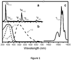
- Figure 1 shows optical spectra for the organic materials in accordance with a specific embodiment of the invention.
- Figure 1(a) presents the absorption spectrum for a single crystal of Er(F-TPIP) 3 showing characteristic absorption into the Er 3+ transitions (all the transitions shown are from the 4 I 15/2 ground state and labelled according to the excited state, using standard nomenclature). Of particular note, there is no ligand absorption in the visible region of the spectra.
- Figure 1(b) which shows the excitation spectrum of the doped film at an emission wavelength of 1.532 ⁇ m (black solid line) 1.1, direct excitation into the erbium ions was too weak to be recorded.
- the dotted line 1.2 is the absorption spectrum for a film of the chromophore Zn(F-BTZ) 2 .
- the dashed line 1.3 is the photoluminescence spectrum for Zn(F-BTZ) 2 powder.
- Figure 1(c) shows the infrared photoluminescence 4 I 13/2 ⁇ 4 I 15/2 from the erbium atoms in the doped film excited at a wavelength of 405nm.
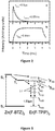
- Figure 2 shows the time dependence of the erbium 1532nm photoluminescence from the doped film.
- it is excited using a 5ns pulse at 417nm excitation and in Figure 2(b) it is excited using a square 4ms pulse at 405nm.
- the long rise time is due to the build-up in the triplet population in the chromophore which is the reservoir through which the erbium ions are excited.
- the Jablonski diagram Figure 3
- Dashed arrows 3.1 represent non-radiative decay.
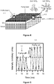
- FIG 4 is a schematic diagram of the waveguide structure used for the gain measurements.
- a probe laser 4.1 was used to excite photoluminescence in the waveguide which was measured at the opposite edge 4.2.
- the graph ( Figure 5 ) shows the intensity of the signal with 5.2 and without 5.1 a pump laser. The presence of the pump laser amplifies the signal intensity by ⁇ 100%.
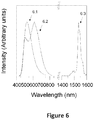
- Figure 6 shows the normalised electroluminescence from an organic light emitting diode (OLED) using a layer of pure Zn(F-BTZ) 2 . Two peaks are observed 6.2: singlet emission at ⁇ 500nm and triplet emission at ⁇ 610nm. In the device where the Zn(F-BTZ) 2 is doped with 20% Er(F-TPIP) 3 the triplet emission can no longer be seen 6.1 and there is strong infrared luminescence from the erbium at ⁇ 1.532 ⁇ m 6.3.
- an erbium complex that does not demonstrate sensitisation in the visible region, but which provides a long luminescence lifetime for the encapsulated erbium ions, is co-evaporated with a halogenated organic chromophore.
- the erbium complex is erbium(III) tetrakis(pentafluorophenyl)-imidodiphosphinate, Er(F-TPIP) 3 and the chromophore is a perfluorinated zinc-based organic chromophore, the zinc(II) salt of 2-(3,4,5,6-tetrafluoro-2-hydroxyphenyl)-4,5,6,7-tetrafluorobenzothiazole, Zn(F-BTZ) 2 .
- This approach is vacuum compatible and high quality films may typically be grown on to any conventional substrate.
- Time resolved photoluminescence measurements at the erbium emission wavelength of 1532nm ( Figure 2a ) recorded using 5ns pulses at a wavelength of 417nm (near the peak of the excitation spectrum and away from any direct Er 3+ ion absorption) show a rise time of ⁇ 0.5 ⁇ s followed by a decay which has at least two components with an average lifetime of ⁇ 0.86 ms.
- the intrinsic radiative lifetime of Er 3+ ions as derived from the corresponding 4 I 15/2 ⁇ 4 I 13//2 absorption spectrum using a single crystal of Er(F-TPIP) 3 , is 13ms for this transition indicating a quantum efficiency of ⁇ 7%.
- Such high photoluminescence efficiency, coupled with the high sensitisation, is critical for population inversion and thus gain.
- the 0.5 ⁇ s rise time is therefore mainly contributed by the conversion of initially populated levels in the Er 3+ ions (arrow 21 in the Jablonski diagram of Figure 3 ) into the emissive 4 I 13/2 state.
- the population in the triplet state of the Zn(F-BTZ) 2 increases with continuing excitation due to the long lifetime of the triplet state under optical excitation ( ⁇ 270 ⁇ s).
- the triplet therefore acts as a reservoir for transfer into the Er 3+ ions (arrows 22 in the Jablonski diagram).
- FIG. 6 shows the electroluminescence spectrum from a layer of pure Zn(F-BTZ) 2 . Two peaks are clearly visible. The higher energy peak is due to the singlet state and has a short lifetime ( ⁇ 100 ns). The lower energy peak is due to the triplet state and has two lifetime components, a major one at ⁇ 50 ⁇ s and a smaller component at ⁇ 5 ⁇ s.
- the signal translating device could be an optical splitter. In current splitters the signal intensity is reduced at each division therefore a 64 way splitter reduces the intensity at each output to 1/64th the input signal. If we made this out of our material then we would amplify the signal at the same time so that there would be no losses at all. Another variant would be multiplexers, where again gain to be integrated into the device instead of them being inherently lossy.
- the invention may be applied to the fabrication of lasers.
- One embodiment could be a simple vertical cavity structure with a dielectric mirror at the bottom and a gold top mirror.
- the dielectric mirror would be transparent to the excitation wavelength but there may be lasing within the cavity.
- a second embodiment could use a distributed Bragg reflector either within a waveguide similar to that used by our prior optical amplifier or with a different period to get a vertical emission.
- Signal translating devices could be integrated onto a single piece of silicon to produce optical integrated circuits.
- An advantage which amplifiers produced in accordance with this invention have over conventional erbium doped fibre amplifiers is that a laser pump is no longer required to get high gain.
- a cheap energy source such as an indium gallium nitride diode may be used or it may be energised using an organic light emitting diode.
- a silicon substrate with a silicon dioxide surface layer is masked to form a spiral structure, the silicon dioxide is etched away to leave a ridge of silicon dioxide and then the organic layer is evaporated to form the waveguide and that will have a gain which may be of the order of 20dB.
- the purified Er(F-TPIP) 3 powder was dissolved in >99.5% Dimethyl Sulfoxide (DMSO) (Sigma-Aldrich). Pink crystals precipitated at room temperature after slow solvent evaporation for a week and were then filtered off. Single crystal X-ray diffraction studies were performed on the same crystal that was used for absorption spectrum. Structures were solved and refined using the Bruker SHELXTL Software Package. Absorption spectra on the crystal were obtained via a homemade single-beam micro-absorption setup with a randomly oriented crystal flatly deposited on a quartz substrate and focused by corresponding Cassegrain and Mitutoyo glass objectives.
- DMSO Dimethyl Sulfoxide
- A denotes the integrated area of absorption band, N is the Er 3+ concentration and L is the thickness of the sample.
- the factor [9 / (n2 + 2)2] represents the local field correction of electric dipole transition.
- Measured line strengths provide the radiative decay coefficient corresponding to each transition:
- a J ′ ⁇ J 64 ⁇ 4 e 3 3 h 2 J + 1 ⁇ ⁇ 3 n n 2 + 2 2 9 S meas J ⁇ J ′
- the measurement of the delayed spectrum and triplet lifetime in Zn(F-BTZ) 2 films was performed by exciting at 430 nm with an OPO (Vibrant II, Opotek) and detecting with an iCCD S20 Gen II Horiba Jobin-Yvon intensified CCD. The light was dispersed with a TRIAX320 monochromator.
- Doped films were grown by co-evaporation at a base pressure of ⁇ 10 -7 mBar. Evaporation rates were independently controlled using two quartz crystal film thickness monitors. Evaporation rates were controlled so that the total deposition rate was at most 0.2 nm/s. Evaporation rates were initially calibrated using film thickness measurements using a Dektak 3. The calibration of molecule ratio in co-doped film was confirmed using energy dispersive x-ray analysis (EDX) on a FEI Quanta 3D ESEM.
- EDX energy dispersive x-ray analysis
- PL photoluminescence
- OPO Continuum Panther Optical Parametric Oscillator
- SLI-10 Continuum Surelite Nd:YAG.
- the laser pulse is 5 ns.
- a 405nm laser was modulated with a TTL signal to give 4ms pulses with a rise/decay time of ⁇ 20 ns.
- Luminescence was focused and filtered onto the adjustable entrance slits of the Jobin Yvon Horiba Triax 550 spectrometer and detected using Hamamatsu R5509-72 liquid nitrogen-cooled detector.
- Excitation spectra were obtained by using a homemade continuous monochromic system.
- a xenon lamp was filtered and focused into a Jobin-Yvon Horiba Triax 180 spectrometer equipped with 1200 lines/mm gratings.
- the monochromatic light from the output of Triax 180 was focused into the co-doped film as ⁇ 1 mm light spot.
- the illumination intensity on the sample was measured directly by a calibrated Newport 918D-UV-OD3R silicon photodetector to normalise the excitation spectra for variations in illumination intensity.
- the luminescence of 1.532 ⁇ m was focused into a Jobin-Yvon Horiba Triax 550 equipped with 600 lines/ mm gratings.
- 1.532 ⁇ m luminescence was detected using a Hamamatsu R5509-72 nitrogen-cooled detector and measured using a 7265 DSP Perkin Elmer lock-in amplifier.
- the waveguide was deposited on a 700 nm thermally grown silicon dioxide layer on a silicon substrate.
- the refractive index of co-doped film was measured via the Jobin Yvon ellipsometer and fitted using a Lorentz oscillator model.
- the refractive index of co-doped film at 1.5 ⁇ m is 1.65 compared to 1.44 for the silicon dioxide layer.
- the silicon substrate was cut to a 20 ⁇ 20 mm 2 square and a 2 ⁇ m of 30% Er(F-TPIP) 3 co-doped Zn(F-BTZ) 2 layer was deposited onto a 10 x 10 mm 2 area in the center.
- the concentration of erbium ions in the waveguide is ⁇ 1.8 x 10 20 cm -3 .
- the silicon substrate was then cleaved through the organic layer to give an abrupt edge to the waveguide which was of length 8mm.
- the probe laser at a wavelength of 405 nm and a power of ⁇ 5 mW, was modulated at 190 Hz and focused into the circle of -400 ⁇ m on one edge of the organic layer.
- the pump laser also at 405 nm but with an initial power of 5 mW, was modulated at 19 Hz and synced to the probe laser.
- This beam was expanded to a diameter of ⁇ 2 cm and then focused using a cylindrical lens to a ⁇ 320 ⁇ m wide and 0.8 cm long stripe which overlapped the probe beam.
- We estimate the pump power on the stripe to be ⁇ 3 mW.
- the light from the cleaved edge of waveguide was focused and filtered onto the adjustable entrance slits of the Jobin Yvon Horiba Triax 550 spectrometer and collected by Hamamatsu R5509-72 nitrogen-cooled detector.
- the measured signal can be seen in figure 10 .
- the 190Hz probe luminescence can be seen superimposed onto the 19 Hz pump luminescence.
- the difference in the intensity of the probe beam, with and without the pump, can be used to calculate the absolute optical gain.
- To determine the internal net gain we have to remove the losses within the waveguide. These losses are primarily due to absorption by the Er(F-TPIP) 3 .
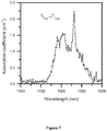
- Figure 7 gives the absorption spectra for this material and given that our layer is doped with 30% Er(F-TPIP) 3 we have taken 0.3 of the absolute absorption to calculate a minimum internal net gain of at least 1.0 dB/cm. The gain was determined by taking an average of 4 measurements.
- Our waveguide is a simple asymmetric slab waveguide with a 2 ⁇ m organic core layer of refractive index, n 1 , a 700 nm silicon dioxide lower cladding layer of refractive index, n 2 , and air as the upper cladding layer of refractive index, n 3 , with an interface 13 between upper cladding layer (air) and core, and an interface 12 between core and the lower cladding layer (silicon dioxide).
- the propagation behavior of this planar waveguide can be modeled using a simple ray-optical approach (reference 1).
- the eigenvalue function or dispersion relationship is used to define the distribution of the propagation modes in the waveguide structure.
- T 2 n 1 2 n 2 2 s ⁇ 2 ⁇ 1
- T 3 n 1 2 n 3 2 s ⁇ 3 ⁇ 1
- P, V and Q are employed to generalize the eigenvalue function.
- P is the normalized propagation constant
- V is the normalized core thickness
- V k 0 n 1 2 ⁇ n 2 2 1 / 2 b
- Q n 1 2 ⁇ n 3 2 n 1 2 ⁇ n 2 2
- the normalized eigenvalue function is: 1 ⁇ P 1 / 2
- V m ⁇ + arctan P 1 ⁇ P 1 / 2 + arctan P + Q 1 ⁇ P 1 / 2 ⁇ is the propagation constant along the waveguide.
- ⁇ x 2 TE 1 ⁇ 2
- ⁇ x 3 TE 1 ⁇ 3
- b effTE b + ⁇ x 2 TE + ⁇ x 3
- ⁇ x 2 TM n 1 2 n 2 2 ⁇ 1 2 ⁇ ⁇ 2 2 ⁇ 2 n 2 4 ⁇ 1 2 + n 1 4 ⁇ 2 2
- ⁇ x 3 TM n 1 2 n 3 2 ⁇ 1 2 ⁇ ⁇ 3 2 ⁇ 3 n 3 4 ⁇ 1 2 + n 1 4 ⁇ 3 2
- b effTM b + ⁇ x 2 TM + ⁇ x 3 TM
- n 1 of the organic core layer is 1.65
- n 2 of the thermally grown SiO 2 is 1.44
- n 3 of air is 1.
- the thickness, b, of the core layer is 2 ⁇ m.
- the thickness of SiO 2 cladding layer is 700 nm.
- any doped erbium medium would have weak absorption of 1.5 ⁇ m, which would cause absorption loss.
- ⁇ complex, the calculation is non-trivial and therefore a perturbation method is generally used to estimate the attenuation coefficient corresponding to the structure and propagation parameters that are estimated with non-loss conditions (reference 6, reference 7).
- the first-order perturbation calculation of the Helmholtz equation gives the general expressions of attenuation coefficients for the TE and TM modes, where we define the attenuation coefficient ⁇ 1 , ⁇ 2 and ⁇ 3 in core layer, substrate layer and cladding layer, respectively:
- the attenuation coefficients of the silicon dioxide layer, ⁇ 2 , and air, ⁇ 3 are taken as zero.
- the attenuation coefficient is only 10 5 less than propagation constant in the waveguide so that the attenuation coefficient makes some difference to the propagation constant and electromagnetic distribution in the waveguide.
- E y x H y x ⁇ A exp ⁇ 2 x ⁇ ⁇ ⁇ x ⁇ 0 : substrate A cos ⁇ 1 x + T 2 sin ⁇ 1 x 0 ⁇ x ⁇ b : core A cos ⁇ 2 b + T 2 sin ⁇ 2 b exp ⁇ ⁇ 3 x ⁇ b b ⁇ x ⁇ + ⁇ : cladding Similar expressions are suitable for E y (x) of TE mode and H y (x) of TM mode.
- 2 z ⁇ ; For TM mode: S ⁇ ⁇ 2 ⁇ 0 ⁇ 1
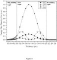
- the energy flux density along the waveguide depth is plotted in Figure 11 .
- the waveguide depth is defined as 0 ⁇ m at the interface between organic core and SiO 2 substrate, and the waveguide depth at 2 ⁇ m is the interface between organic core and cladding layer of air. It can therefore be calculated that 96% of the light is propagating in the organic core.
- the emissive layer was a film of Zn(F-BTZ) 2 (20 nm) for the undoped device, or the same thickness film of Zn(F-BTZ) 2 co-evaporated with 20% Er(F-TPIP) 3 for the codoped device.
- a 50 nm thickness film of aluminum 8-hydroxyquinolinate (Alq 3 ) was used as an electron transport layer (ETL).
- the cathode consisted of 1 nm LiF with 100 nm of aluminum.
Landscapes
- Chemical & Material Sciences (AREA)
- Physics & Mathematics (AREA)
- Inorganic Chemistry (AREA)
- Engineering & Computer Science (AREA)
- Materials Engineering (AREA)
- Condensed Matter Physics & Semiconductors (AREA)
- General Physics & Mathematics (AREA)
- Electromagnetism (AREA)
- Optics & Photonics (AREA)
- Nonlinear Science (AREA)
- Crystallography & Structural Chemistry (AREA)
- Lasers (AREA)
Description
- This invention relates to optoelectronic devices, to methods of fabrication of such devices, to signal translating systems incorporating these devices and to materials for use therein.
- According to Bohr's quantum mechanical model, an atom may only exist in certain permitted energy states. The application of this theory to optoelectronic devices is set out in
Chapter 2 of Fibre Optic Lasers and Amplifiers edited by P.W. France (France 1991Figure 2.3 (p20) of France 1991 illustrate the permitted energy transitions for various dopants in different glass hosts. -
PCT patent application WO8701246A1 - As a result of these attributes, useful laser action or amplifier gain can be produced for less commonplace rare-earth or transition metal dopants and for less commonplace optical transitions, even where the optical transitions involved are inherently weak. Room temperature continuous laser operation has even been found possible for 3-level laser systems which had previously only operated in a pulsed mode.
- Since the dopant concentration is so low, manufacture can be economical. A typical device might use as little as 0.1µg of dopant oxide.
- Silica, if selected as the host medium, has good power handling characteristics. Moreover in the presence of a high-silica glass host, the optical transitions of the rare-earth or transition metal dopant ions are substantially broadened. This permits the realisation of both tunable lasers and broad-band amplifiers.
- Most rare-earth dopants and some transition metal dopants have now been investigated experimentally. Remarkably, all exhibit windows in which losses are low notwithstanding the close proximity of high-loss absorption bands. This enables the construction of extremely long amplifiers and lasers.
- In summary, the active devices provide improved sources/amplifiers for telecommunications applications because they can handle high powers without damage, they provide smaller/lighter/cheaper general purpose active devices and may in conjunction with other fibre devices (eg gratings) provide new and powerful signal processing functions. Note also that non-linear effects can be readily achieved at the optical power levels obtained in fibre lasers, affording exploitation of a number of simultaneous laser and nonlinear effects. However, it is not feasible to increase the radiation yield indefinitely by increasing dopant concentrations because at high concentrations the close proximity of neighbouring ions causes losses, a phenomenon known as concentration quenching. In order to achieve optimum performance of fibre rare-earth doped lasers and amplifiers it was necessary to fabricate them from preforms prepared by a modified chemical vapour deposition process which gave a low concentration of the dopant. A similar effect may be achieved by incorporating the dopant into an organic ligand.
- Modern telecommunications are based on a worldwide network of silica fibre-optic cables which encircle the globe carrying data at the speed of light. Despite the low losses experienced in these fibres it is still necessary to amplify the optical signals regularly and this has hitherto been performed by means of erbium doped fibre amplifiers (EDFAs). These rely on an intra-atomic transition in the erbium ion that emits at a wavelength of 1.5µm, the low loss window of silica fibres. Due to the weak excitation properties of erbium ions, a separate pump laser must be launched axially down erbium doped fibres of 10-30 m length to achieve sufficient population inversion and thus optical gain. The properties of erbium-based amplifiers can, in principle, be enhanced by incorporating erbium ions into organic hosts containing chromophores that couple to the erbium (this phenomenon is called sensitisation), which allows for pumping with lower intensity sources, such as light emitting diodes (LEDs) and amplification in much shorter lengths. Attempts to implement this idea have been hampered by the quenching of the erbium ions by CH or OH oscillators present in most organic compounds. We have found that we can couple the long fluorescence lifetimes of erbium in a halogenated organic ligand with a fully halogenated chromophore to produce a system with exceptional sensitisation (> 104 relative to direct absorption) coupled with an internal quantum efficiency of ∼7%. This system has been implemented into planar amplifying waveguides of the type described in our patent application
WO0178203A1 - Despite over 10 years of work on organic erbium complexes there has hitherto been remarkably little progress in making systems with sufficiently promising properties to be considered for use in optical amplifiers or lasers. Although on the one hand, some organic chromophores have been shown to sensitise the erbium in suitable spectral ranges and, on the other hand some deuterated and halogenated (even perfluorinated) complexes show a considerable enhancement of the erbium emission properties and provide relatively long lifetimes, the reality is that both conditions are never fulfilled to an operational extent. One of the problems with producing perfluorinated ligands and chromophores is that the strongly electron withdrawing properties of the fluorine atoms makes it difficult for the ligands to bind with lanthanide ions and many of the compounds are not chemically or thermally stable. Apart from the synthesis-related problems, this represents an extra difficulty towards processing the materials via a conventional organic vapour deposition technique, which has been employed to achieve the purity and optical quality required for signal translating applications.
- We have overcome these problems by separating the chromophore function (strong absorption in the organic group) from that of producing a high efficiency organic environment for the erbium ion (strong, long lived 1.5µm emission) whilst creating a highly efficient energy transfer between the two.
- According to the present invention there is provided an optoelectronic signal translating device according to
claim 1. In an example, there is a device having a region containing rare earth or transition metal ions with permitted upper and lower energy states for generation of radiation of a predetermined wavelength by means of a transition between said energy states wherein said region includes an organic complex comprising a ligand adapted to enhance the emission of radiation by conservation of ions in said upper energy state and a chromophore separately co-operable with a radiation source of wavelength not greater than that of said predetermined desired radiation to excite said chromophore to cross-couple with either the upper permitted energy state or to a higher energy state of said rare earth or transition metal ions from which said ions decay to said upper permitted state thereby to generate said predetermined desired radiation by the subsequent decay of said ions to the permitted lower energy state. - A journal article by Wang et al (J. Phys. Chem, B, 2004, 108, p. 8084-8088) describes enhanced luminescence of an erbium (III) ion-association ternary complex with a near-infrared dye. Wang describes use of a partially halogenated ligand with an erbium ion, together with a chromophore.
-
US 2002/0197050 describes a method and apparatus for producing near-infrared radiation. The system describes use of a metal-ligand complex and partially halogenated luminescent polymer. - The present invention will be particularly described with reference to the accompanying drawings in which:-
-
Figure 1a, 1b and 1c show optical spectra for certain organic materials -
Figures 2a and 2b show the time dependence of erbium 1532nm photoluminescence from a doped film -
Figure 3 is a Jablonski diagram showing energy transfer transitions in a preferred embodiment of the invention -
Figure 4 is a schematic diagram of a waveguide structure used for gain measurements: -
Figure 5 is graph showing signal intensity measurements taken from the waveguide; and -
Figure 6 shows the normalised electroluminescence from an organic light emitting diode (OLED) using a layer of pure Zn(F-BTZ)2 and the corresponding electroluminescence from a doped device - Referring now to the drawings,
Figure 1 shows optical spectra for the organic materials in accordance with a specific embodiment of the invention.Figure 1(a) presents the absorption spectrum for a single crystal of Er(F-TPIP)3 showing characteristic absorption into the Er3+ transitions (all the transitions shown are from the 4I15/2 ground state and labelled according to the excited state, using standard nomenclature). Of particular note, there is no ligand absorption in the visible region of the spectra. InFigure 1(b) , which shows the excitation spectrum of the doped film at an emission wavelength of 1.532µm (black solid line) 1.1, direct excitation into the erbium ions was too weak to be recorded. The dotted line 1.2 is the absorption spectrum for a film of the chromophore Zn(F-BTZ)2. The dashed line 1.3 is the photoluminescence spectrum for Zn(F-BTZ)2 powder.Figure 1(c) shows the infrared photoluminescence 4I13/2 → 4I15/2 from the erbium atoms in the doped film excited at a wavelength of 405nm. -
Figure 2 shows the time dependence of the erbium 1532nm photoluminescence from the doped film. InFigure 2(a) it is excited using a 5ns pulse at 417nm excitation and inFigure 2(b) it is excited using a square 4ms pulse at 405nm. The long rise time is due to the build-up in the triplet population in the chromophore which is the reservoir through which the erbium ions are excited. Also shown is the Jablonski diagram (Figure 3 ) for the system highlighting the energy transfer from both the singlet S0, S1 and triplet states T1 in the Zn(F-BTZ)2. Dashed arrows 3.1 represent non-radiative decay. -
Figure 4 is a schematic diagram of the waveguide structure used for the gain measurements. A probe laser 4.1 was used to excite photoluminescence in the waveguide which was measured at the opposite edge 4.2. The graph (Figure 5 ) shows the intensity of the signal with 5.2 and without 5.1 a pump laser. The presence of the pump laser amplifies the signal intensity by ∼100%. -
Figure 6 shows the normalised electroluminescence from an organic light emitting diode (OLED) using a layer of pure Zn(F-BTZ)2. Two peaks are observed 6.2: singlet emission at ∼500nm and triplet emission at ∼610nm. In the device where the Zn(F-BTZ)2 is doped with 20% Er(F-TPIP)3 the triplet emission can no longer be seen 6.1 and there is strong infrared luminescence from the erbium at ∼1.532µm 6.3. - In a preferred embodiment of the invention an erbium complex that does not demonstrate sensitisation in the visible region, but which provides a long luminescence lifetime for the encapsulated erbium ions, is co-evaporated with a halogenated organic chromophore.
- In a specific embodiment of the invention the erbium complex is erbium(III) tetrakis(pentafluorophenyl)-imidodiphosphinate, Er(F-TPIP)3 and the chromophore is a perfluorinated zinc-based organic chromophore, the zinc(II) salt of 2-(3,4,5,6-tetrafluoro-2-hydroxyphenyl)-4,5,6,7-tetrafluorobenzothiazole, Zn(F-BTZ)2. This approach is vacuum compatible and high quality films may typically be grown on to any conventional substrate. We have used this approach to grow a 2µm thick organic waveguide, on to a 700nm thermally grown silicon dioxide layer on a silicon substrate. The resulting waveguide demonstrated a gain coefficient of 3.3dB/cm at a wavelength of 1.532µm, whilst optically pumped (5mW) at a wavelength of 405nm. Additionally, we have demonstrated that the active layer can be implemented into a 1.5µm emitting organic light emitting diode (OLED). This technology may be used to produce organic optical amplifiers and lasers operating at the key telecommunications wavelength of 1.5µm.
- The absorption spectrum for a 100µm crystal of Er(F-TPIP)3 is presented in
Figure 1a ; it can be seen that there is clear absorption directly into the Er3+ ions but no evidence of ligand absorption at wavelengths greater than 350nm. In contrastFigure 1b shows the excitation spectrum, recorded at the Er3+ emission wavelength of 1532nm, for a 250nm thick film of Zn(F-BTZ)2, co-evaporated with 30% Er(F-TPIP)3. Hence in this doped film there is no evidence of direct absorption into the Er3+ ions and the excitation is dominated by a broad band which extends from the UV at <350nm to ∼475nm in the blue. This excitation spectrum matches well to the emission from commercially available and highly efficient high-power blue light emitting diodes (LEDs). - As the excitation spectrum shows no evidence of direct absorption into the erbium ion we are only able to give a minimum value for the enhancement of sensitisation provided by the Zn(F-BTZ)2 complex. The ratio of the size of the integrated area under the excitation spectrum from 350nm to 500nm to that measured in the region from 510nm to 540nm, which includes the strong 520nm 2H11/2→4I15/2 transition, gives a minimum sensitisation for the doped film in the order of 104, relative to direct absorption into the Er3+ ion. In order to demonstrate that this sensitisation is directly attributable to the Zn(F-BTZ)2 complex we show in
Figure 1b the absorption spectrum from a 250nm thick layer of pure Zn(F-BTZ)2. This absorption spectrum has a band that is coincident with that for the excitation spectrum of the doped layer, demonstrating that it is the Zn complex that sensitises the erbium emission. The infrared photoluminescence spectrum of the doped Zn(F-BTZ)2 film when excited at a wavelength of 405nm is shown inFigure 1c . The emission spectrum shows strong luminescence from the 4I13/2→4I15/2 transition centred at ∼1532nm. - Crucial information on the nature of the sensitisation and energy transfer processes can be gained from time resolved measurements. Time resolved photoluminescence measurements at the erbium emission wavelength of 1532nm (
Figure 2a ) recorded using 5ns pulses at a wavelength of 417nm (near the peak of the excitation spectrum and away from any direct Er3+ ion absorption) show a rise time of ∼0.5 µs followed by a decay which has at least two components with an average lifetime of ∼0.86 ms. The intrinsic radiative lifetime of Er3+ ions, as derived from the corresponding 4I15/2→4I13//2 absorption spectrum using a single crystal of Er(F-TPIP)3, is 13ms for this transition indicating a quantum efficiency of ∼7%. Such high photoluminescence efficiency, coupled with the high sensitisation, is critical for population inversion and thus gain. - We can describe the observed energy transfer processes from an organic chromophore into the Er3+ ion in a Jablonski diagram (
Figure 3 ). Absorption of a photon in the organic moiety generates singlet excitons, S1. A change in spin number is required to transfer the excitation from the organic S1 state to the Er3+ multiplets and that a prior change from the singlet into a lower lying triplet state, T1 (inter-system crossing) allows this coupling to occur more efficiently. In this system the effect of the eight fluorine atoms on each benzothiazole ligand favours the spin mixing and intersystem crossing through the enhanced spin-orbit interaction caused by the high Z of fluorine and hence contributes to efficiently transferring the energy to the Er3+ multiplets directly and via the intermediate state T1. - The time evolution of the erbium 1532nm emission when excited using square modulation of length 4ms from a 405nm laser, which again is only absorbed by the Zn(F-BTZ)2 chromophore, is illustrated in
Figure 2b . Compared with the excitation using the 5ns pulsed laser, the longer pulse gives a greatly increased rise time of 0.8ms. This different behaviour can be explained if we consider that for the short pulse there is no time to build up a significant population in the triplet state and it is expected that the primary energy transfer into the Er3+ ions will be through the short lived (<100 ns) singlet state in the Zn(F-BTZ)2. The 0.5µs rise time is therefore mainly contributed by the conversion of initially populated levels in the Er3+ ions (arrow 21 in the Jablonski diagram ofFigure 3 ) into the emissive 4I13/2 state. However, for the long excitation time the population in the triplet state of the Zn(F-BTZ)2 increases with continuing excitation due to the long lifetime of the triplet state under optical excitation (∼270µs). The triplet therefore acts as a reservoir for transfer into the Er3+ ions (arrows 22 in the Jablonski diagram). - The sensitisation and luminescence properties of the Zn(F-BTZ)2 - Er(F-TPIP)3 system make it an ideal candidate for use as an optical amplifier operating at telecommunications wavelengths. We have fabricated a waveguide formed from a 2µm evaporated film of Zn(F-BTZ)2 doped with 25% Er(F-TPIP)3 on to a 700nm thermally grown silicon dioxide layer on a silicon substrate.
Figure 5 shows the intensity of the 1.5µm luminescence (modulated at 190Hz) observed from the edge of the waveguide, with and without an optical pump. It can be clearly seen that the intensity of the modulated probe signal is amplified by ∼100% when the pump laser is switched on. This gives a gain of 3.3 dB/cm at 1.532µm in this waveguide structure. - While the optically pumped system which we have demonstrated can be widely utilised for optical gain as it is compatible with cheap, highly efficient, high-power LEDs further applications of this system are possible if the erbium ions are excited electrically. We have therefore demonstrated that Er(F-TPIP)3 doped Zn(F-BTZ)2 can be used to produce IR OLEDs.
Figure 6 shows the electroluminescence spectrum from a layer of pure Zn(F-BTZ)2. Two peaks are clearly visible. The higher energy peak is due to the singlet state and has a short lifetime (<100 ns). The lower energy peak is due to the triplet state and has two lifetime components, a major one at ∼ 50µs and a smaller component at ∼5µs. These are somewhat lower than the 270µs we have measured in a pulse photoluminescence experiment and can probably be attributed to quenching of the triplets in the OLED. One possible mechanism that is known to occur is triplet-polaron quenching, although there may be other mechanisms present such as triplet-triplet annihilation due to the much higher triplet population present in the OLED. The strong triplet emission observed in this device is evidence of the efficiency of the spin mixing between the singlet and triplet states due to the presence of the fluorine on the ligand.Figure 6 also shows the 1.5µm electroluminescence from an OLED where the Zn(F-BTZ)2 was doped with 20% of Er(F-TPIP)3 which demonstrates that efficient electrical pumping of this system is possible. In this doped OLED the visible emission is solely due to the singlet emission and this is probably caused by triplet quenching due to efficient coupling into the Er3+ ions in the Er(F-TPIP)3. - We have demonstrated a new system for producing high efficiency, sensitised infrared luminescence from erbium ions that is based on the separation of the absorption and emission functions and by having efficient energy transfer between them. This separation allows for much greater control over the individual functions which gives us fine control over the properties through design at a molecular scale. The approach is fully compatible with vacuum processing and can be deposited onto any substrate. We have used this approach to fabricate a simple planar waveguide on silicon and have demonstrated optical gain of 3.3dB/cm at a wavelength of 1.532µm, using a pump intensity of only 5mW. We have also fabricated an OLED using the same active layer which demonstrates significant emissions from erbium. This approach makes possible new hybrid integrated optoelectronic devices and applications such as organic optical amplifiers and lasers which can be easily integrated into other materials systems.
- Whilst we have specifically described certain preferred embodiments, it will be apparent to one skilled in the art that various modifications may be made without departing from the ambit of the invention as defined in the claims. For example, there is a range of transition metal complexes using heavier ions than Zn (e.g. Ir and Pt) which have almost 100% transformation from singlet to triplet. These could be made using halogenated ligands. The signal translating device could be an optical splitter. In current splitters the signal intensity is reduced at each division therefore a 64 way splitter reduces the intensity at each output to 1/64th the input signal. If we made this out of our material then we would amplify the signal at the same time so that there would be no losses at all. Another variant would be multiplexers, where again gain to be integrated into the device instead of them being inherently lossy.
- The invention may be applied to the fabrication of lasers. One embodiment could be a simple vertical cavity structure with a dielectric mirror at the bottom and a gold top mirror. The dielectric mirror would be transparent to the excitation wavelength but there may be lasing within the cavity. A second embodiment could use a distributed Bragg reflector either within a waveguide similar to that used by our prior optical amplifier or with a different period to get a vertical emission.
- Signal translating devices could be integrated onto a single piece of silicon to produce optical integrated circuits.
- An advantage which amplifiers produced in accordance with this invention have over conventional erbium doped fibre amplifiers is that a laser pump is no longer required to get high gain. A cheap energy source such as an indium gallium nitride diode may be used or it may be energised using an organic light emitting diode.
- In another embodiment a silicon substrate with a silicon dioxide surface layer is masked to form a spiral structure, the silicon dioxide is etched away to leave a ridge of silicon dioxide and then the organic layer is evaporated to form the waveguide and that will have a gain which may be of the order of 20dB.
-
-
Figure 7 shows the absorption spectrum between 1400 nm and 1600 nm of a Er(F-TPIP)3 crystal. -
Figure 8 shows the photoluminescence decay of the triplet emission in Zn(F-BTZ)2. -
Figure 9 shows the delayed (Δt = 50 µs) photoluminescence emission of Zn(F-BTZ)2. The spectrum shows the triplet emission, which matches the broad low energy band observed in electroluminescence (see main text). -
Figure 10 shows the photoluminescence from the edge of the waveguide. The 190 Hz modulation can be seen to be amplified when the pump laser is on. -
Figure 11 shows energy flux density along the waveguide depth. - Following synthesis both Er(F-TPIP)3 and Zn(F-BTZ)2 were purified by train sublimation under 10-7 mbar vacuum prior to use.
- The purified Er(F-TPIP)3 powder was dissolved in >99.5% Dimethyl Sulfoxide (DMSO) (Sigma-Aldrich). Pink crystals precipitated at room temperature after slow solvent evaporation for a week and were then filtered off. Single crystal X-ray diffraction studies were performed on the same crystal that was used for absorption spectrum. Structures were solved and refined using the Bruker SHELXTL Software Package. Absorption spectra on the crystal were obtained via a homemade single-beam micro-absorption setup with a randomly oriented crystal flatly deposited on a quartz substrate and focused by corresponding Cassegrain and Mitutoyo glass objectives. Absorption spectrum from 1400nm-1600nm were taken using a tungsten lamp and a
Triax 550 monochromator equipped with 600 lines/mm gratings. Light detection was using a Hamamatsu R5509-72 liquid nitrogen-cooled detector. Signals were measured using a 7265 DSP Perkin Elmer lock-in amplifier and recorded with the resolution of 2nm (figure 7 ) . The Becke line test with calibrated liquids (Cargille) was employed to estimate an averaged value for the refractive index of microcrystals. The crystal thicknesses were measured by a graduated microscope equipped with a micropositioning stage (accuracy = 5 µm). - The line strengths S(J→J') of specific electronic transitions of Er3+ ions are determined using the following expression:

λ is the mean wavelength of special absorption bands. J' and J are the quantum numbers of total angular momentum of the initial state and the excited state, respectively and n is the refractive index of the host material. The average refractive index of the crystal employed in measurement of absorption spectra was measured to be 1.65 by Becke line test. Γ is the integrated absorption coefficient, Γ = ∫ ε(λ)dλ, where ε is the absorption coefficient which we determine from the absorption spectra by ε=A/ (NL). A denotes the integrated area of absorption band, N is the Er3+ concentration and L is the thickness of the sample. The factor [9/(n2+2)2] represents the local field correction of electric dipole transition. - Measured line strengths provide the radiative decay coefficient corresponding to each transition:

- The radiative lifetime


- The absorption spectrum from 1400-1600nm is extracted with the resolution of 2 nm in
Figure 7 . - The measurement of the delayed spectrum and triplet lifetime in Zn(F-BTZ)2 films was performed by exciting at 430 nm with an OPO (Vibrant II, Opotek) and detecting with an iCCD S20 Gen II Horiba Jobin-Yvon intensified CCD. The light was dispersed with a TRIAX320 monochromator.
- The lifetime was measured by integrating the 40 times averaged emission centered at 685 nm with a changing delay of 50-850 µs and counting for 1100 us (
figure 8 ).Figure 9 shows the delayed luminescence spectrum. - Doped films were grown by co-evaporation at a base pressure of ∼10-7 mBar. Evaporation rates were independently controlled using two quartz crystal film thickness monitors. Evaporation rates were controlled so that the total deposition rate was at most 0.2 nm/s. Evaporation rates were initially calibrated using film thickness measurements using a
Dektak 3. The calibration of molecule ratio in co-doped film was confirmed using energy dispersive x-ray analysis (EDX) on a FEI Quanta 3D ESEM. - For the nanosecond pulsed photoluminescence (PL) experiments excitation was from a Continuum Panther Optical Parametric Oscillator (OPO) laser pumped by a Continuum Surelite (SLI-10) Nd:YAG. The laser pulse is 5 ns. For the millisecond pulsed measurements a 405nm laser was modulated with a TTL signal to give 4ms pulses with a rise/decay time of <20 ns. Luminescence was focused and filtered onto the adjustable entrance slits of the Jobin
Yvon Horiba Triax 550 spectrometer and detected using Hamamatsu R5509-72 liquid nitrogen-cooled detector. - Excitation spectra were obtained by using a homemade continuous monochromic system. A xenon lamp was filtered and focused into a Jobin-Yvon Horiba Triax 180 spectrometer equipped with 1200 lines/mm gratings. The monochromatic light from the output of Triax 180 was focused into the co-doped film as ∼1 mm light spot. The illumination intensity on the sample was measured directly by a calibrated Newport 918D-UV-OD3R silicon photodetector to normalise the excitation spectra for variations in illumination intensity. The luminescence of 1.532 µm was focused into a Jobin-
Yvon Horiba Triax 550 equipped with 600 lines/ mm gratings. 1.532 µm luminescence was detected using a Hamamatsu R5509-72 nitrogen-cooled detector and measured using a 7265 DSP Perkin Elmer lock-in amplifier. - The waveguide was deposited on a 700 nm thermally grown silicon dioxide layer on a silicon substrate.
- The refractive index of co-doped film was measured via the Jobin Yvon ellipsometer and fitted using a Lorentz oscillator model. The refractive index of co-doped film at 1.5 µm is 1.65 compared to 1.44 for the silicon dioxide layer.
- The silicon substrate was cut to a 20 × 20 mm2 square and a 2 µm of 30% Er(F-TPIP)3 co-doped Zn(F-BTZ)2 layer was deposited onto a 10 x 10 mm2 area in the center. The concentration of erbium ions in the waveguide is ∼1.8 x 1020 cm-3. The silicon substrate was then cleaved through the organic layer to give an abrupt edge to the waveguide which was of length 8mm.
- The probe laser, at a wavelength of 405 nm and a power of ∼5 mW, was modulated at 190 Hz and focused into the circle of -400 µm on one edge of the organic layer. The pump laser, also at 405 nm but with an initial power of 5 mW, was modulated at 19 Hz and synced to the probe laser. This beam was expanded to a diameter of ∼2 cm and then focused using a cylindrical lens to a ∼ 320 µm wide and 0.8 cm long stripe which overlapped the probe beam. We estimate the pump power on the stripe to be ∼3 mW.
- The light from the cleaved edge of waveguide was focused and filtered onto the adjustable entrance slits of the Jobin
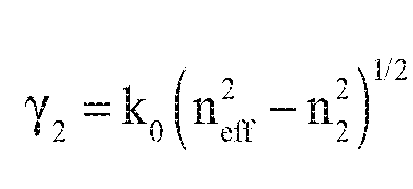
Yvon Horiba Triax 550 spectrometer and collected by Hamamatsu R5509-72 nitrogen-cooled detector. The measured signal can be seen infigure 10 . The 190Hz probe luminescence can be seen superimposed onto the 19 Hz pump luminescence. The difference in the intensity of the probe beam, with and without the pump, can be used to calculate the absolute optical gain. To determine the internal net gain we have to remove the losses within the waveguide. These losses are primarily due to absorption by the Er(F-TPIP)3.Figure 7 gives the absorption spectra for this material and given that our layer is doped with 30% Er(F-TPIP)3 we have taken 0.3 of the absolute absorption to calculate a minimum internal net gain of at least 1.0 dB/cm. The gain was determined by taking an average of 4 measurements. - Our waveguide is a simple asymmetric slab waveguide with a 2 µm organic core layer of refractive index, n1, a 700 nm silicon dioxide lower cladding layer of refractive index, n2 , and air as the upper cladding layer of refractive index, n3, with an interface 13 between upper cladding layer (air) and core, and an interface 12 between core and the lower cladding layer (silicon dioxide). The propagation behavior of this planar waveguide can be modeled using a simple ray-optical approach (reference 1).
- Snell's law states that



- In the case that n1 > n2 > n3, the situation of total internal reflection at both interfaces will cause the phase shift -2Φ12 and -2Φ13 (
reference 2, reference 3), where atinterface 12,
interface 13,
- We can simplify the phase shifts by defining T 2=γ 2 lγ 1 and T 3 = γ 3 / γ 1 giving -2Φ12 = -2arctanT 2 and - 2Φ13 = -2arctanT 3.
- The eigenvalue function or dispersion relationship is used to define the distribution of the propagation modes in the waveguide structure. The total phase shift, which happens both in interface 12 and interface 13 satisfies2γ 1 b - 2Φ12 - 2Φ13 = 2mπ, so the eigenvalue function (reference 4) is,




reference 3, reference 5). Therefore, Δz is given byΔz = dΦ /dβ. Using these expressions, the penetration depth in the twocladding layers
For the TE mode:

- In our planar waveguide at a wavelength of 1.5 pm, n1 of the organic core layer is 1.65, n2 of the thermally grown SiO2 is 1.44 and n3 of air is 1. The thickness, b, of the core layer is 2µm. The thickness of SiO2 cladding layer is 700 nm. Numerical calculation shows that TE0, TM0, TE1 and TM1 modes exist in the waveguide structure. The propagation constants of each mode can be obtained through numerical solutions of eigenvalue function. The propagation constant, effective index, penetration depth and effective waveguide thickness of each guide mode are listed in the Table 1.
Table 1: Propagation constant, effective index, penetration depth and effective waveguide thickness Mode Propagation Constant β Effective Refractive Index N=β/k0 Penetration Depth (Substrate) Δx2 Attenuation Coefficient α Effective Core Thickness beff TE0 6.761(106) 1.614 328 nm 54.842 2. 6 µm TE1 6.414(106) 1.531 459 nm 64.020 2.7 µm TM0 6.755 (106) 1.613 272 nm 65.592 2.4 µm TM1 6.391(106) 1.526 485 nm 61.692 2.7 µm - Any doped erbium medium would have weak absorption of 1.5 µm, which would cause absorption loss. The attenuation loss yields a complex propagation constant in an absorbing medium, β̃ = β - iα where α is attenuation coefficient of the amplitude of the propagation mode. Considering that β̃ is complex, the calculation is non-trivial and therefore a perturbation method is generally used to estimate the attenuation coefficient corresponding to the structure and propagation parameters that are estimated with non-loss conditions (reference 6, reference 7). The first-order perturbation calculation of the Helmholtz equation gives the general expressions of attenuation coefficients for the TE and TM modes, where we define the attenuation coefficient α 1, α 2 and α 3 in core layer, substrate layer and cladding layer, respectively:


- Obviously, the attenuation coefficient is only 105 less than propagation constant in the waveguide so that the attenuation coefficient makes some difference to the propagation constant and electromagnetic distribution in the waveguide.
- The distribution fields for TE and TM modes as expressed:

For TE mode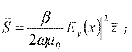

Figure 11 . The waveguide depth is defined as 0 µm at the interface between organic core and SiO2 substrate, and the waveguide depth at 2 µm is the interface between organic core and cladding layer of air. It can therefore be calculated that 96% of the light is propagating in the organic core. - All the layers were deposited in a high-vacuum (10-8 mbar) Kurt J. Lesker thermal evaporation system onto a clean patterned ITO substrate. The thickness of each layer was measured by an in-situ quartz crystal monitor. 3,3'-dimethyl-N4,N4,N4',N4'-tetra-m-tolyl-[1,1'-biphenyl]-4,4'-diamine (HMTPD) (50 nm) was used as the hole injection and transport layer. The emissive layer (EML) was a film of Zn(F-BTZ)2 (20 nm) for the undoped device, or the same thickness film of Zn(F-BTZ)2 co-evaporated with 20% Er(F-TPIP)3 for the codoped device. A 50 nm thickness film of aluminum 8-hydroxyquinolinate (Alq3) was used as an electron transport layer (ETL). The cathode consisted of 1 nm LiF with 100 nm of aluminum.
-
- 1. H. Kogelnik: Theory of dielectric waveguides, in Integrated Optics, T. Tamir (ed.), 2nd edn., Topics Appl. Phys., Vol. 7 (Springer, Berlin, Heidelberg 1979) Chap. 2
- 2. M. Born, E. Wolf: Principles of Optics, 3rd edn. (Pergamon, New York 1970) p.49
- 3. K. Artmann, Ann. Physik, 1948, 2, 87.
- 4. H.K.V. Lotsch, Optik, , 32, 116, 189, 299, 553, (1970).
- 5. K. Zhang, D. Li, et al, Electromagnetic theory for microwaves and optoelectronics Second Edition, p.344,1998
- 6. J. Kane and H.J. Osterberg, Opt. Soc. Am., 1964, 54, 347
- 7. A. Reisinger, Appl. Opt., 1973, 12, 1015
Claims (13)
- An optically active material comprising an organic complex containing rare earth or transition metal ions with permitted upper and lower energy states for generation of radiation of a predetermined wavelength by means of a transition between said energy states, the organic complex comprising a halogenated ligand adapted to enhance the emission of radiation by conservation of ions in said upper energy state, the optically active material further comprising a chromophore separately co-operable with a radiation source of wavelength not greater than that of said predetermined desired radiation to excite said chromophore to cross-couple with either the upper permitted energy state or to a higher energy state of said rare earth or transition metal ions from which said ions decay to said upper permitted state thereby to generate said predetermined desired radiation by the subsequent decay of said ions to the permitted lower energy state, characterised in that the chromophore is halogenated.
- The optically active material according to claim 1 wherein said chromophore uses a phosphorescent material for mixing of singlet and triplet states to enhance the triplet population.
- The optically active material according to claim 1 or claim 2 wherein said organic complex comprises a fluorinated ligand or a chlorinated ligand.
- The optically active material according to claim 1 or claim 2 wherein the halogenated chromophore is fluorinated or chlorinated.
- The optically active material according to claim 1 or claim 2 wherein said organic complex is erbium(III) tetrakis(pentafluorophenyl)-imidodiphosphinate, Er(F-TPIP)3 and said chromophore is the zinc(II) salt of 2-(3,4,5,6-tetrafluoro-2-hydroxyphenyl)-4,5,6,7-tetrafluorobenzothiazole, Zn(F- BTZ)2.
- An optical amplifier comprising a waveguide formed from the optically active material of claim 1, wherein the optically active material is an evaporated film of Zn(F-BTZ)2 doped with substantially 25% Er(F-TPIP)3 on a silicon dioxide layer on a silicon substrate.
- An optoelectronic signal translating device having a region including the optically active material of any one of claims 1 to 5.
- A method of fabricating an optoelectronic device comprising the step of codepositing an organic complex of a rare earth or transition metal element which has a relatively long fluorescence lifetime, said organic complex comprising a halogenated ligand to enhance the emission of radiation by conservation of ions in said upper energy state, said organic complex deposited together with a chromophore which does not demonstrate sensitisation at a wavelength on the vicinity of that of the fluorescence of said organic complex wherein said chromophore can transfer energy absorbed from a radiation source to said organic complex to excite it to generate radiation at a desired predetermined wavelength characteristic of said organic complex to enhance the emission of radiation by conservation of ions in said upper energy state, characterised in that the chromophore is halogenated.
- The method of fabricating an optoelectronic signal translating device according to claim 8 wherein said organic complex comprises a fluorinated ligand or a chlorinated ligand.
- The method of fabricating an optoelectronic signal translating device according to claim 8 wherein said chromophore is fluorinated or chlorinated.
- The method of fabricating an optoelectronic device according to claim 8 wherein said organic complex is erbium(III) tetrakis(pentafluorophenyl)-imidodiphosphinate, Er(F-TPIP)3 and said chromophore is the zinc(II) salt of 2-(3,4,5,6-tetrafluoro-2-hydroxyphenyl)-4,5,6,7-tetrafluorobenzothiazole, Zn(F- BTZ)2.
- A method of fabricating an optical amplifier according to any one of claims 8 to 11.
- A method of fabricating an organic light emitting device according to any one of claims 8 to 11.
Applications Claiming Priority (2)
| Application Number | Priority Date | Filing Date | Title |
|---|---|---|---|
| GB201311862A GB201311862D0 (en) | 2013-07-02 | 2013-07-02 | Optoelectronic devices, methods of fabrication thereof and materials therefor |
| PCT/GB2014/052011 WO2015001338A1 (en) | 2013-07-02 | 2014-07-02 | Optoelectronic devices, methods of fabrication thereof and materials therefor |
Publications (2)
| Publication Number | Publication Date |
|---|---|
| EP3017489A1 EP3017489A1 (en) | 2016-05-11 |
| EP3017489B1 true EP3017489B1 (en) | 2021-06-23 |
Family
ID=48999396
Family Applications (1)
| Application Number | Title | Priority Date | Filing Date |
|---|---|---|---|
| EP14736935.9A Active EP3017489B1 (en) | 2013-07-02 | 2014-07-02 | Materials for optoelectronic devices and method of fabrication of an optoelectronic device |
Country Status (5)
| Country | Link |
|---|---|
| US (1) | US9837794B2 (en) |
| EP (1) | EP3017489B1 (en) |
| CN (2) | CN105659406B (en) |
| GB (1) | GB201311862D0 (en) |
| WO (1) | WO2015001338A1 (en) |
Families Citing this family (7)
| Publication number | Priority date | Publication date | Assignee | Title |
|---|---|---|---|---|
| US9923634B2 (en) | 2015-09-23 | 2018-03-20 | Fujitsu Limited | Harmonic generation and phase sensitive amplification using a bragg reflection waveguide |
| US11539190B2 (en) | 2016-09-02 | 2022-12-27 | Kyushu University, National University Corporation | Continuous-wave organic thin-film distributed feedback laser and electrically driven organic semiconductor laser diode |
| CN109792134B (en) | 2017-02-07 | 2022-08-16 | 国立大学法人九州大学 | Current injection type organic semiconductor laser diode, method for manufacturing the same, and program |
| CN108956556B (en) * | 2018-05-18 | 2021-06-25 | 复旦大学 | A luminescent probe and time-resolved fluorescence detection system |
| GB201812765D0 (en) | 2018-08-06 | 2018-09-19 | Univ London Queen Mary | Substrate layer |
| CN111146686B (en) * | 2019-12-27 | 2021-03-02 | 华中科技大学 | A Near-Mid-Infrared Broadband Light Source Based on Multi-layer Special-shaped Array Hole Structure |
| US11588290B2 (en) * | 2019-12-30 | 2023-02-21 | Raytheon Company | Methods and apparatus for generating ghost light |
Family Cites Families (9)
| Publication number | Priority date | Publication date | Assignee | Title |
|---|---|---|---|---|
| CN1245516A (en) * | 1996-11-27 | 2000-02-23 | 伊斯曼化学公司 | Process for preparing light-absorbing polymer compositions |
| US6579630B2 (en) * | 2000-12-07 | 2003-06-17 | Canon Kabushiki Kaisha | Deuterated semiconducting organic compounds used for opto-electronic devices |
| US7928278B2 (en) * | 2001-06-12 | 2011-04-19 | University Of Florida Research Foundation, Inc. | Method and apparatus for producing near-infrared radiation |
| US20030099424A1 (en) * | 2001-08-24 | 2003-05-29 | Yousef Mohajer | Optical gain media and methods for making and using same |
| US7449724B2 (en) * | 2003-09-12 | 2008-11-11 | Semiconductor Energy Laboratory Co., Ltd. | Light-emitting device |
| US7502392B2 (en) * | 2003-09-12 | 2009-03-10 | Semiconductor Energy Laboratory Co., Ltd. | Laser oscillator |
| US7260135B2 (en) * | 2003-09-26 | 2007-08-21 | Semiconductor Energy Laboratory Co., Ltd. | Light emitting device |
| US20090295274A1 (en) * | 2008-02-04 | 2009-12-03 | Kuo-Chu Hwang | Deuterated Semiconducting Organic Compounds for Use in Light-Emitting Devices |
| CN102231035B (en) * | 2011-05-30 | 2013-05-22 | 武汉邮电科学研究院 | All optical wavelength converter and all optical wavelength conversion method for dual-semiconductor optical amplifier structure |
-
2013
- 2013-07-02 GB GB201311862A patent/GB201311862D0/en not_active Ceased
-
2014
- 2014-07-02 WO PCT/GB2014/052011 patent/WO2015001338A1/en not_active Ceased
- 2014-07-02 CN CN201480048236.0A patent/CN105659406B/en active Active
- 2014-07-02 EP EP14736935.9A patent/EP3017489B1/en active Active
- 2014-07-02 US US14/902,104 patent/US9837794B2/en active Active
- 2014-07-02 CN CN201910230855.6A patent/CN110265556B/en active Active
Non-Patent Citations (1)
| Title |
|---|
| None * |
Also Published As
| Publication number | Publication date |
|---|---|
| WO2015001338A1 (en) | 2015-01-08 |
| CN110265556A (en) | 2019-09-20 |
| CN105659406B (en) | 2019-04-23 |
| GB201311862D0 (en) | 2013-08-14 |
| EP3017489A1 (en) | 2016-05-11 |
| CN105659406A (en) | 2016-06-08 |
| US20160141838A1 (en) | 2016-05-19 |
| US9837794B2 (en) | 2017-12-05 |
| CN110265556B (en) | 2021-10-29 |
Similar Documents
| Publication | Publication Date | Title |
|---|---|---|
| US9837794B2 (en) | Optoelectronic devices, methods of fabrication thereof and materials therefor | |
| CA2096183C (en) | Erbium doped optical devices | |
| Vasdekis et al. | Diode pumped distributed Bragg reflector lasers based on a dye-to-polymer energy transfer blend | |
| CA3155407C (en) | Integrated silicon structures with optical gain mediated by rare-earth-doped tellurium-oxide-coating | |
| Cheng et al. | Experimental realization of a PbSe quantum dot doped fiber amplifier with ultra-bandwidth characteristic | |
| Zeng et al. | Achieving low threshold and high optical gain amplified spontaneous emission in MAPbI3 perovskite films via symmetric waveguide effect | |
| WO2008117249A1 (en) | Integrated optical waveguide amplifier or laser with rare earth ions and sensitizer elements co-doped core and related optical pumping method | |
| Unal et al. | Neodymium-doped tantalum pentoxide waveguide lasers | |
| Tong et al. | Spectroscopy of thulium-doped tantalum pentoxide waveguides on silicon | |
| Subramanian et al. | Erbium-doped waveguide laser in tantalum pentoxide | |
| Soriano‐Díaz et al. | Photon Recycling Triggered Amplified Spontaneous Emission in MAPbBr3‐Ni (AcO) 2 Nanocomposite Waveguides | |
| Palatnik et al. | Solid-state Rhodamine 6G microcavity laser | |
| Vasdekis et al. | Silicon based organic semiconductor laser | |
| Pollnau | Rare-earth-ion-doped waveguide lasers on a silicon chip | |
| Zhu et al. | Hybrid colloidal quantum dot silicon nitride waveguide gain measurement based on variable stripe length method | |
| Choudhary et al. | On-chip rare-earth-doped lasers | |
| Soriano-Díaz et al. | Amplified spontaneous emission and lasing in perovskite nanocomposites | |
| US8385375B2 (en) | P-element doped laser medium apparatus and method | |
| Wang et al. | Thulium-Doped Al 2 O 3 Waveguide Amplifiers Fabricated via Radio Frequency Reactive Co-Sputtering | |
| Samuel | Towards polymer lasers and amplifiers | |
| Suárez et al. | Waveguide Amplifiers and Lasers Based on FASnI 3 Perovskite Thin Films | |
| Woli et al. | Silver nanocube-assisted random lasing of perovskite materials | |
| Singh et al. | Watt-class CMOS-compatible optical high power amplifier | |
| Zhu et al. | On-chip low-threshold silicon nitride distributed feedback colloidal quantum dot laser | |
| Bradley et al. | 2.0 dB/cm gain in an Al 2 O 3: Er 3+ waveguide on silicon |
Legal Events
| Date | Code | Title | Description |
|---|---|---|---|
| PUAI | Public reference made under article 153(3) epc to a published international application that has entered the european phase |
Free format text: ORIGINAL CODE: 0009012 |
|
| 17P | Request for examination filed |
Effective date: 20160129 |
|
| AK | Designated contracting states |
Kind code of ref document: A1 Designated state(s): AL AT BE BG CH CY CZ DE DK EE ES FI FR GB GR HR HU IE IS IT LI LT LU LV MC MK MT NL NO PL PT RO RS SE SI SK SM TR |
|
| AX | Request for extension of the european patent |
Extension state: BA ME |
|
| DAX | Request for extension of the european patent (deleted) | ||
| STAA | Information on the status of an ep patent application or granted ep patent |
Free format text: STATUS: EXAMINATION IS IN PROGRESS |
|
| 17Q | First examination report despatched |
Effective date: 20190128 |
|
| REG | Reference to a national code |
Ref country code: DE Ref legal event code: R079 Ref document number: 602014078272 Country of ref document: DE Free format text: PREVIOUS MAIN CLASS: H01L0051540000 Ipc: H01S0003160000 |
|
| GRAP | Despatch of communication of intention to grant a patent |
Free format text: ORIGINAL CODE: EPIDOSNIGR1 |
|
| STAA | Information on the status of an ep patent application or granted ep patent |
Free format text: STATUS: GRANT OF PATENT IS INTENDED |
|
| RIC1 | Information provided on ipc code assigned before grant |
Ipc: H01L 51/54 20060101ALI20210112BHEP Ipc: H01S 3/16 20060101AFI20210112BHEP |
|
| INTG | Intention to grant announced |
Effective date: 20210203 |
|
| GRAS | Grant fee paid |
Free format text: ORIGINAL CODE: EPIDOSNIGR3 |
|
| GRAA | (expected) grant |
Free format text: ORIGINAL CODE: 0009210 |
|
| STAA | Information on the status of an ep patent application or granted ep patent |
Free format text: STATUS: THE PATENT HAS BEEN GRANTED |
|
| AK | Designated contracting states |
Kind code of ref document: B1 Designated state(s): AL AT BE BG CH CY CZ DE DK EE ES FI FR GB GR HR HU IE IS IT LI LT LU LV MC MK MT NL NO PL PT RO RS SE SI SK SM TR |
|
| REG | Reference to a national code |
Ref country code: GB Ref legal event code: FG4D |
|
| REG | Reference to a national code |
Ref country code: CH Ref legal event code: EP |
|
| REG | Reference to a national code |
Ref country code: DE Ref legal event code: R096 Ref document number: 602014078272 Country of ref document: DE Ref country code: AT Ref legal event code: REF Ref document number: 1405127 Country of ref document: AT Kind code of ref document: T Effective date: 20210715 |
|
| REG | Reference to a national code |
Ref country code: IE Ref legal event code: FG4D |
|
| REG | Reference to a national code |
Ref country code: LT Ref legal event code: MG9D |
|
| PG25 | Lapsed in a contracting state [announced via postgrant information from national office to epo] |
Ref country code: FI Free format text: LAPSE BECAUSE OF FAILURE TO SUBMIT A TRANSLATION OF THE DESCRIPTION OR TO PAY THE FEE WITHIN THE PRESCRIBED TIME-LIMIT Effective date: 20210623 Ref country code: LT Free format text: LAPSE BECAUSE OF FAILURE TO SUBMIT A TRANSLATION OF THE DESCRIPTION OR TO PAY THE FEE WITHIN THE PRESCRIBED TIME-LIMIT Effective date: 20210623 Ref country code: BG Free format text: LAPSE BECAUSE OF FAILURE TO SUBMIT A TRANSLATION OF THE DESCRIPTION OR TO PAY THE FEE WITHIN THE PRESCRIBED TIME-LIMIT Effective date: 20210923 Ref country code: HR Free format text: LAPSE BECAUSE OF FAILURE TO SUBMIT A TRANSLATION OF THE DESCRIPTION OR TO PAY THE FEE WITHIN THE PRESCRIBED TIME-LIMIT Effective date: 20210623 |
|
| REG | Reference to a national code |
Ref country code: AT Ref legal event code: MK05 Ref document number: 1405127 Country of ref document: AT Kind code of ref document: T Effective date: 20210623 |
|
| PG25 | Lapsed in a contracting state [announced via postgrant information from national office to epo] |
Ref country code: GR Free format text: LAPSE BECAUSE OF FAILURE TO SUBMIT A TRANSLATION OF THE DESCRIPTION OR TO PAY THE FEE WITHIN THE PRESCRIBED TIME-LIMIT Effective date: 20210924 Ref country code: LV Free format text: LAPSE BECAUSE OF FAILURE TO SUBMIT A TRANSLATION OF THE DESCRIPTION OR TO PAY THE FEE WITHIN THE PRESCRIBED TIME-LIMIT Effective date: 20210623 Ref country code: NO Free format text: LAPSE BECAUSE OF FAILURE TO SUBMIT A TRANSLATION OF THE DESCRIPTION OR TO PAY THE FEE WITHIN THE PRESCRIBED TIME-LIMIT Effective date: 20210923 Ref country code: RS Free format text: LAPSE BECAUSE OF FAILURE TO SUBMIT A TRANSLATION OF THE DESCRIPTION OR TO PAY THE FEE WITHIN THE PRESCRIBED TIME-LIMIT Effective date: 20210623 Ref country code: SE Free format text: LAPSE BECAUSE OF FAILURE TO SUBMIT A TRANSLATION OF THE DESCRIPTION OR TO PAY THE FEE WITHIN THE PRESCRIBED TIME-LIMIT Effective date: 20210623 |
|
| REG | Reference to a national code |
Ref country code: NL Ref legal event code: MP Effective date: 20210623 |
|
| PG25 | Lapsed in a contracting state [announced via postgrant information from national office to epo] |
Ref country code: CZ Free format text: LAPSE BECAUSE OF FAILURE TO SUBMIT A TRANSLATION OF THE DESCRIPTION OR TO PAY THE FEE WITHIN THE PRESCRIBED TIME-LIMIT Effective date: 20210623 Ref country code: EE Free format text: LAPSE BECAUSE OF FAILURE TO SUBMIT A TRANSLATION OF THE DESCRIPTION OR TO PAY THE FEE WITHIN THE PRESCRIBED TIME-LIMIT Effective date: 20210623 Ref country code: SM Free format text: LAPSE BECAUSE OF FAILURE TO SUBMIT A TRANSLATION OF THE DESCRIPTION OR TO PAY THE FEE WITHIN THE PRESCRIBED TIME-LIMIT Effective date: 20210623 Ref country code: SK Free format text: LAPSE BECAUSE OF FAILURE TO SUBMIT A TRANSLATION OF THE DESCRIPTION OR TO PAY THE FEE WITHIN THE PRESCRIBED TIME-LIMIT Effective date: 20210623 Ref country code: AT Free format text: LAPSE BECAUSE OF FAILURE TO SUBMIT A TRANSLATION OF THE DESCRIPTION OR TO PAY THE FEE WITHIN THE PRESCRIBED TIME-LIMIT Effective date: 20210623 Ref country code: ES Free format text: LAPSE BECAUSE OF FAILURE TO SUBMIT A TRANSLATION OF THE DESCRIPTION OR TO PAY THE FEE WITHIN THE PRESCRIBED TIME-LIMIT Effective date: 20210623 Ref country code: PT Free format text: LAPSE BECAUSE OF FAILURE TO SUBMIT A TRANSLATION OF THE DESCRIPTION OR TO PAY THE FEE WITHIN THE PRESCRIBED TIME-LIMIT Effective date: 20211025 Ref country code: RO Free format text: LAPSE BECAUSE OF FAILURE TO SUBMIT A TRANSLATION OF THE DESCRIPTION OR TO PAY THE FEE WITHIN THE PRESCRIBED TIME-LIMIT Effective date: 20210623 Ref country code: NL Free format text: LAPSE BECAUSE OF FAILURE TO SUBMIT A TRANSLATION OF THE DESCRIPTION OR TO PAY THE FEE WITHIN THE PRESCRIBED TIME-LIMIT Effective date: 20210623 |
|
| PG25 | Lapsed in a contracting state [announced via postgrant information from national office to epo] |
Ref country code: PL Free format text: LAPSE BECAUSE OF FAILURE TO SUBMIT A TRANSLATION OF THE DESCRIPTION OR TO PAY THE FEE WITHIN THE PRESCRIBED TIME-LIMIT Effective date: 20210623 |
|
| REG | Reference to a national code |
Ref country code: CH Ref legal event code: PL |
|
| REG | Reference to a national code |
Ref country code: DE Ref legal event code: R097 Ref document number: 602014078272 Country of ref document: DE |
|
| PG25 | Lapsed in a contracting state [announced via postgrant information from national office to epo] |
Ref country code: MC Free format text: LAPSE BECAUSE OF FAILURE TO SUBMIT A TRANSLATION OF THE DESCRIPTION OR TO PAY THE FEE WITHIN THE PRESCRIBED TIME-LIMIT Effective date: 20210623 |
|
| REG | Reference to a national code |
Ref country code: BE Ref legal event code: MM Effective date: 20210731 |
|
| PG25 | Lapsed in a contracting state [announced via postgrant information from national office to epo] |
Ref country code: LI Free format text: LAPSE BECAUSE OF NON-PAYMENT OF DUE FEES Effective date: 20210731 Ref country code: DK Free format text: LAPSE BECAUSE OF FAILURE TO SUBMIT A TRANSLATION OF THE DESCRIPTION OR TO PAY THE FEE WITHIN THE PRESCRIBED TIME-LIMIT Effective date: 20210623 Ref country code: CH Free format text: LAPSE BECAUSE OF NON-PAYMENT OF DUE FEES Effective date: 20210731 |
|
| PLBE | No opposition filed within time limit |
Free format text: ORIGINAL CODE: 0009261 |
|
| STAA | Information on the status of an ep patent application or granted ep patent |
Free format text: STATUS: NO OPPOSITION FILED WITHIN TIME LIMIT |
|
| 26N | No opposition filed |
Effective date: 20220324 |
|
| PG25 | Lapsed in a contracting state [announced via postgrant information from national office to epo] |
Ref country code: LU Free format text: LAPSE BECAUSE OF NON-PAYMENT OF DUE FEES Effective date: 20210702 Ref country code: AL Free format text: LAPSE BECAUSE OF FAILURE TO SUBMIT A TRANSLATION OF THE DESCRIPTION OR TO PAY THE FEE WITHIN THE PRESCRIBED TIME-LIMIT Effective date: 20210623 |
|
| PG25 | Lapsed in a contracting state [announced via postgrant information from national office to epo] |
Ref country code: IT Free format text: LAPSE BECAUSE OF FAILURE TO SUBMIT A TRANSLATION OF THE DESCRIPTION OR TO PAY THE FEE WITHIN THE PRESCRIBED TIME-LIMIT Effective date: 20210623 Ref country code: IE Free format text: LAPSE BECAUSE OF NON-PAYMENT OF DUE FEES Effective date: 20210702 Ref country code: BE Free format text: LAPSE BECAUSE OF NON-PAYMENT OF DUE FEES Effective date: 20210731 |
|
| PG25 | Lapsed in a contracting state [announced via postgrant information from national office to epo] |
Ref country code: HU Free format text: LAPSE BECAUSE OF FAILURE TO SUBMIT A TRANSLATION OF THE DESCRIPTION OR TO PAY THE FEE WITHIN THE PRESCRIBED TIME-LIMIT; INVALID AB INITIO Effective date: 20140702 |
|
| PG25 | Lapsed in a contracting state [announced via postgrant information from national office to epo] |
Ref country code: CY Free format text: LAPSE BECAUSE OF FAILURE TO SUBMIT A TRANSLATION OF THE DESCRIPTION OR TO PAY THE FEE WITHIN THE PRESCRIBED TIME-LIMIT Effective date: 20210623 |
|
| PG25 | Lapsed in a contracting state [announced via postgrant information from national office to epo] |
Ref country code: MK Free format text: LAPSE BECAUSE OF FAILURE TO SUBMIT A TRANSLATION OF THE DESCRIPTION OR TO PAY THE FEE WITHIN THE PRESCRIBED TIME-LIMIT Effective date: 20210623 |
|
| PG25 | Lapsed in a contracting state [announced via postgrant information from national office to epo] |
Ref country code: MT Free format text: LAPSE BECAUSE OF FAILURE TO SUBMIT A TRANSLATION OF THE DESCRIPTION OR TO PAY THE FEE WITHIN THE PRESCRIBED TIME-LIMIT Effective date: 20210623 |
|
| PGFP | Annual fee paid to national office [announced via postgrant information from national office to epo] |
Ref country code: GB Payment date: 20250613 Year of fee payment: 12 |
|
| PGFP | Annual fee paid to national office [announced via postgrant information from national office to epo] |
Ref country code: FR Payment date: 20250613 Year of fee payment: 12 |
|
| PGFP | Annual fee paid to national office [announced via postgrant information from national office to epo] |
Ref country code: DE Payment date: 20250617 Year of fee payment: 12 |
|
| PG25 | Lapsed in a contracting state [announced via postgrant information from national office to epo] |
Ref country code: TR Free format text: LAPSE BECAUSE OF FAILURE TO SUBMIT A TRANSLATION OF THE DESCRIPTION OR TO PAY THE FEE WITHIN THE PRESCRIBED TIME-LIMIT Effective date: 20210623 |