EP3016163A1 - Laminate and manufacturing method therefor - Google Patents
Laminate and manufacturing method therefor Download PDFInfo
- Publication number
- EP3016163A1 EP3016163A1 EP14847748.2A EP14847748A EP3016163A1 EP 3016163 A1 EP3016163 A1 EP 3016163A1 EP 14847748 A EP14847748 A EP 14847748A EP 3016163 A1 EP3016163 A1 EP 3016163A1
- Authority
- EP
- European Patent Office
- Prior art keywords
- layer
- laminate
- substrate
- conductive layer
- conductive
- Prior art date
- Legal status (The legal status is an assumption and is not a legal conclusion. Google has not performed a legal analysis and makes no representation as to the accuracy of the status listed.)
- Granted
Links
Images
Classifications
-
- H—ELECTRICITY
- H10—SEMICONDUCTOR DEVICES; ELECTRIC SOLID-STATE DEVICES NOT OTHERWISE PROVIDED FOR
- H10K—ORGANIC ELECTRIC SOLID-STATE DEVICES
- H10K50/00—Organic light-emitting devices
- H10K50/80—Constructional details
- H10K50/805—Electrodes
-
- H—ELECTRICITY
- H10—SEMICONDUCTOR DEVICES; ELECTRIC SOLID-STATE DEVICES NOT OTHERWISE PROVIDED FOR
- H10K—ORGANIC ELECTRIC SOLID-STATE DEVICES
- H10K59/00—Integrated devices, or assemblies of multiple devices, comprising at least one organic light-emitting element covered by group H10K50/00
- H10K59/80—Constructional details
- H10K59/805—Electrodes
- H10K59/8051—Anodes
- H10K59/80516—Anodes combined with auxiliary electrodes, e.g. ITO layer combined with metal lines
-
- B—PERFORMING OPERATIONS; TRANSPORTING
- B32—LAYERED PRODUCTS
- B32B—LAYERED PRODUCTS, i.e. PRODUCTS BUILT-UP OF STRATA OF FLAT OR NON-FLAT, e.g. CELLULAR OR HONEYCOMB, FORM
- B32B15/00—Layered products comprising a layer of metal
- B32B15/04—Layered products comprising a layer of metal comprising metal as the main or only constituent of a layer, which is next to another layer of the same or of a different material
-
- H—ELECTRICITY
- H10—SEMICONDUCTOR DEVICES; ELECTRIC SOLID-STATE DEVICES NOT OTHERWISE PROVIDED FOR
- H10K—ORGANIC ELECTRIC SOLID-STATE DEVICES
- H10K50/00—Organic light-emitting devices
-
- H—ELECTRICITY
- H10—SEMICONDUCTOR DEVICES; ELECTRIC SOLID-STATE DEVICES NOT OTHERWISE PROVIDED FOR
- H10K—ORGANIC ELECTRIC SOLID-STATE DEVICES
- H10K50/00—Organic light-emitting devices
- H10K50/80—Constructional details
- H10K50/805—Electrodes
- H10K50/81—Anodes
- H10K50/814—Anodes combined with auxiliary electrodes, e.g. ITO layer combined with metal lines
-
- H—ELECTRICITY
- H10—SEMICONDUCTOR DEVICES; ELECTRIC SOLID-STATE DEVICES NOT OTHERWISE PROVIDED FOR
- H10K—ORGANIC ELECTRIC SOLID-STATE DEVICES
- H10K50/00—Organic light-emitting devices
- H10K50/80—Constructional details
- H10K50/805—Electrodes
- H10K50/82—Cathodes
- H10K50/824—Cathodes combined with auxiliary electrodes
-
- H—ELECTRICITY
- H10—SEMICONDUCTOR DEVICES; ELECTRIC SOLID-STATE DEVICES NOT OTHERWISE PROVIDED FOR
- H10K—ORGANIC ELECTRIC SOLID-STATE DEVICES
- H10K71/00—Manufacture or treatment specially adapted for the organic devices covered by this subclass
- H10K71/20—Changing the shape of the active layer in the devices, e.g. patterning
- H10K71/231—Changing the shape of the active layer in the devices, e.g. patterning by etching of existing layers
-
- H—ELECTRICITY
- H10—SEMICONDUCTOR DEVICES; ELECTRIC SOLID-STATE DEVICES NOT OTHERWISE PROVIDED FOR
- H10K—ORGANIC ELECTRIC SOLID-STATE DEVICES
- H10K71/00—Manufacture or treatment specially adapted for the organic devices covered by this subclass
- H10K71/60—Forming conductive regions or layers, e.g. electrodes
-
- Y—GENERAL TAGGING OF NEW TECHNOLOGICAL DEVELOPMENTS; GENERAL TAGGING OF CROSS-SECTIONAL TECHNOLOGIES SPANNING OVER SEVERAL SECTIONS OF THE IPC; TECHNICAL SUBJECTS COVERED BY FORMER USPC CROSS-REFERENCE ART COLLECTIONS [XRACs] AND DIGESTS
- Y10—TECHNICAL SUBJECTS COVERED BY FORMER USPC
- Y10T—TECHNICAL SUBJECTS COVERED BY FORMER US CLASSIFICATION
- Y10T428/00—Stock material or miscellaneous articles
- Y10T428/24—Structurally defined web or sheet [e.g., overall dimension, etc.]
- Y10T428/24479—Structurally defined web or sheet [e.g., overall dimension, etc.] including variation in thickness
- Y10T428/24488—Differential nonuniformity at margin
-
- Y—GENERAL TAGGING OF NEW TECHNOLOGICAL DEVELOPMENTS; GENERAL TAGGING OF CROSS-SECTIONAL TECHNOLOGIES SPANNING OVER SEVERAL SECTIONS OF THE IPC; TECHNICAL SUBJECTS COVERED BY FORMER USPC CROSS-REFERENCE ART COLLECTIONS [XRACs] AND DIGESTS
- Y10—TECHNICAL SUBJECTS COVERED BY FORMER USPC
- Y10T—TECHNICAL SUBJECTS COVERED BY FORMER US CLASSIFICATION
- Y10T428/00—Stock material or miscellaneous articles
- Y10T428/24—Structurally defined web or sheet [e.g., overall dimension, etc.]
- Y10T428/24777—Edge feature
Definitions
- the present application relates to a laminate and a method for preparing the same.
- An organic light-emitting element is composed of two opposing electrodes and organic material thin films of a plurality of layers having semiconductor-like properties interposed therebetween.
- the organic light-emitting element having the configuration uses a phenomenon in which electric energy is converted into light energy by using an organic material, that is, an organic light emitting phenomenon. Specifically, when voltage is applied between two electrodes in a structure in which an organic layer is disposed between an anode electrode and an electrode, holes from the anode electrode and electrons from the cathode electrode are injected into the organic material layer. When the injected holes and electrons meet each other, an exciton is formed, and the exciton falls down to a bottom state to emit light.
- the organic light-emitting electrode may be typically classified into a top emission type, a bottom-emission type and a dual emission type.
- the top emission or bottom emission type one of two electrodes needs to be a light transmissive electrode, and in the case of the double-sided emission type, all the two electrodes needs to be a light transmissive electrode.
- the element In order to use the organic light-emitting element as lighting, the element needs to be driven at high brightness unlike the existing natural color display, and a constant brightness needs to be maintained like the existing lighting.
- a high driving current In order to sufficiently improve the brightness of the organic light-emitting element, light emission needs to be implemented in a large area, and in order to implement light emission in the large area, a high driving current needs to be used.
- the aforementioned high current needs to be uniformly injected into the diode having the large area.
- An exemplary embodiment of the present application provides a laminate, including: a substrate; a first layer provided on the substrate; a second layer which is provided on the first layer and has an overhang structure with a width which is larger than that of the first layer; and a conductive layer which is provided on the substrate and the second layer, in which the conductive layer provided on the substrate is electrically shorted from the conductive layer provided on the second layer.
- Another exemplary embodiment of the present application provides a method for preparing a laminate, including: 1) forming a first layer on a substrate; 2) forming a second layer on the first layer, the second layer having an overhang structure whose width is larger than that of the first layer; and 3) forming conductive layers on the substrate and the second layer, the conductive layer provided on the substrate being electrically shorted from the conductive layer provided on the second layer.
- Yet another exemplary embodiment of the present application provides an electrode including the laminate.
- the laminate according to the exemplary embodiment of the present application may be applied to an electrode for an organic light emitting element. Further, in the laminate according to the exemplary embodiment of the present application, electrically shorted conductive layers are formed on the substrate and the overhang structure so that usage of a mask for pattern formation which has been used in the related art during the manufacturing process of a laminate may be avoided. Accordingly, a cost for a manufacturing process of an organic light emitting element may be reduced.
- an organic light-emitting diode for illumination has a structure in which a transparent electrode, an organic material layer, and a metal electrode are sequentially deposited on a substrate.
- deposition patterns of the organic material layer and the metal electrode have different areas on a plan view, and thus different masks are used during the deposition of the organic material layer and the metal electrode. Accordingly, there are problems in that it is necessary to replace the mask during the deposition process, productivity is not high due to a complex deposition equipment, and production costs are also high.
- a laminate according to an exemplary embodiment of the present application includes a substrate; a first layer which is provided on the substrate; a second layer which is provided on the first layer and has an overhang structure with a width which is larger than that of the first layer; and conductive layers which are provided on the substrate and the second layer, in which the conductive layer provided on the substrate is electrically shorted from the conductive layer provided on the second layer.
- the conductive layer provided on the substrate may be electrically shorted from the first layer and the conductive layer provided on the substrate may be electrically shorted from the second layer.
- the first layer may be provided not on the entire surface of the substrate, but on a part of the substrate.
- the electrically shorted structure means that two layers are physically separated from each other and structurally disposed to be spaced apart from each other.
- a mask for pattern formation is used to form a conductive layer having an electrically shorted structure, that is, a conductive pattern on a substrate.
- conductive layers are formed on the substrate and a double layer having an overhang structure formed on the substrate so that a conductive pattern including a structure in which a conductive layer formed on the substrate and a conductive layer formed on the double layer having an overhang structure are electrically shorted from each other may be prepared, without using a separate mask for pattern formation.
- a second layer having an overhang structure whose width is larger than that of the first layer may be formed such that the first layer and the second layer include materials whose etching speeds by the same etchant are different from each other. That is, the second layer may include a material whose etching speed by the same etchant is lower than that of the first layer.
- the second layer having the overhang structure may be formed by varying a type of etchant which is used when the first layer and the second layer are formed.
- the etchant may include hydrofluoric acid (HF), phosphoric acid (H 3 PO 4 ), a buffered oxide etchant (BOE), a buffered HF solution (BHF), hydrogen peroxide-based etchants, CH 3 COOH, HCl, HNO 3 , or ferric-based etchants, but are not limited thereto.
- HF hydrofluoric acid
- H 3 PO 4 phosphoric acid
- BOE buffered oxide etchant
- BHF buffered HF solution
- hydrogen peroxide-based etchants CH 3 COOH, HCl, HNO 3
- ferric-based etchants but are not limited thereto.
- an optimized overhang structure may be formed by appropriately adjusting an etching time and a temperature when an etching process is performed on the first layer and the second layer.
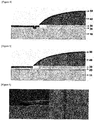
- a photography of the overhang structure according to an exemplary embodiment of the present application is illustrated in FIG. 6 .
- the first layer may be a metal layer and the second layer may be an insulating layer.
- the metal layer may include one or more of magnesium, calcium, sodium, potassium, titanium, indium, lithium, gadolinium, aluminum, silver, tin, lead, chrome, molybdenum, copper, and an alloy thereof, but is not limited thereto.
- a thickness of the metal layer may be from 50 nm to 5 ⁇ m, but is not limited thereto.
- the insulating layer may be formed by using a material and a method known in the art. More specifically, the insulating layer may be formed by using a general photoresist material; polyimide; polyacryl; silicon nitride; silicon oxide; aluminum oxide; aluminum nitride; an alkali metal oxide; an alkaline earth metal oxide, and the like, but is not limited thereto.
- the thickness of the insulating layer may be from 10 nm to 10 ⁇ m, but is not limited thereto.
- a transparent conducting oxide layer may be additionally included between the substrate and the first layer.
- the transparent conducting oxide layer may be additionally included between the substrate and the conductive layer which is formed on the substrate.
- the transparent conducting oxide may be at least one oxide selected from indium (In), tin (Sn), zinc (Zn), gallium (Ga), cerium (Ce), cadmium (Cd), magnesium (Mg), beryllium (Be), silver (Ag), molybdenum (Mo), vanadium (V), copper (Cu), iridium (Ir), rhodium (Rh), ruthenium (Ru), tungsten (W), cobalt (Co), nickel (Ni), manganese (Mn), aluminum (Al) and lanthanum (La).
- oxide selected from indium (In), tin (Sn), zinc (Zn), gallium (Ga), cerium (Ce), cadmium (Cd), magnesium (Mg), beryllium (Be), silver (Ag), molybdenum (Mo), vanadium (V), copper (Cu), iridium (Ir), rhodium (Rh), ruthenium (Ru), tungsten (W),
- the conductive layer may include the transparent conducting oxide.
- the transparent conducting oxide may be at least one oxide selected from indium (In), tin (Sn), zinc (Zn), gallium (Ga), cerium (Ce), cadmium (Cd), magnesium (Mg), beryllium (Be), silver (Ag), molybdenum (Mo), vanadium (V), copper (Cu), iridium (Ir), rhodium (Rh), ruthenium (Ru), tungsten (W), cobalt (Co), nickel (Ni), manganese (Mn), aluminum (Al) and lanthanum (La).
- the conductive layer may include one or more of magnesium, calcium, sodium, potassium, titanium, indium, yttrium, lithium, gadolinium, aluminum, silver, platinum, gold, tungsten, tantalum, copper, tin, lead, and an alloy thoseof.
- the conductive layer may be formed by using any one physical vapor deposition selected from sputtering, E-beam evaporation, thermal evaporation, laser molecular beam epitaxy (L-MBE), and pulsed laser deposition (PLD); any one chemical vapor deposition selected from thermal chemical vapor deposition, plasma-enhanced chemical vapor deposition (PECVD), light chemical vapor deposition, laser chemical vapor deposition, metal-organic chemical vapor deposition (MOCVD) and hydride vapor phase epitaxy (HVPE); or atomic layer deposition (ALD).
- PECVD plasma-enhanced chemical vapor deposition
- MOCVD metal-organic chemical vapor deposition
- HVPE hydride vapor phase epitaxy
- ALD atomic layer deposition
- the thickness of the conductive layer may be 50 nm to 5 ⁇ m, but is not limited thereto.
- the substrate may be formed of transparent plastic or glass, formed of the transparent conducting oxide mentioned above, or formed of one or more of magnesium, calcium, sodium, potassium, titanium, indium, yttrium, lithium, gadolinium, aluminum, silver, tin, lead, chrome, molybdenum, copper, and an alloy thoseof.
- An exemplary embodiment of the present application provides a method for preparing a laminate, including: 1) forming a first layer on a substrate; 2) forming a second layer on the first layer, the second layer having an overhang structure whose width of the second layer is larger than that of the first layer; and 3) forming conductive layers on the substrate and the second layer, the conductive layer provided on the substrate being electrically shorted from the conductive layer provided on the second layer.
- the overhang structure in step 2) may be formed by individually or simultaneously etching the first layer and the second layer.
- the method may further include forming a transparent conducting oxide layer between the substrate and the first layer.
- an electrode according to the exemplary embodiment of the present application may include the laminate.
- the electrode including the laminate may be applied to an organic light emitting element for a display and an organic light emitting element for illumination, but is not limited thereto.
- the conductive layer provided on the second layer may be applied as a cathode electrode and the substrate and the first layer may be applied as an anode electrode and an auxiliary electrode of the anode electrode, but are not limited thereto.
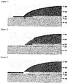
- FIGS. 1 and 2 An electrode for the organic light emitting element of the related art is illustrated in FIGS. 1 and 2 and an electrode for an organic light emitting element including the laminate according to the exemplary embodiment of the present application is illustrated in FIGS. 3 to 5 .
- a mask which is formed of metal is used as a shadow mask. More specifically, during a deposition process of an organic material, one or more shadow masks are used and during a deposition process of the second electrode, one shadow mask is used.
- the metal shadow mask is not necessary so that a manufacturing cost for a mask is reduced and a management cost for regularly washing and replacing the mask is reduced.
- an organic material patterning technique is combined, so that a deposition process in which the mask is not necessary may be configured.
- an equipment conveyance unit may be simplified. Specifically, as a size of equipment and a size of glass are increased, a cost reduction effect in accordance with the simplification as mentioned above is significantly increased.
- the laminate according to the exemplary embodiment of the present application may be applied to an electrode for an organic light emitting element. Further, in the laminate according to the exemplary embodiment of the present application, an electrically shorted conductive layer is formed on the substrate and the overhang structure so that usage of a mask for pattern formation which has been used in the related art during the manufacturing process of a laminate may be avoided. Accordingly, a cost for a manufacturing process of an organic light emitting element may be reduced.
Landscapes
- Physics & Mathematics (AREA)
- Optics & Photonics (AREA)
- Engineering & Computer Science (AREA)
- Manufacturing & Machinery (AREA)
- Electroluminescent Light Sources (AREA)
- Laminated Bodies (AREA)
Abstract
Description
- This application claims priority to and the benefit of Korean Patent Application No.
10-2013-0116197 - The present application relates to a laminate and a method for preparing the same.
- An organic light-emitting element is composed of two opposing electrodes and organic material thin films of a plurality of layers having semiconductor-like properties interposed therebetween. The organic light-emitting element having the configuration uses a phenomenon in which electric energy is converted into light energy by using an organic material, that is, an organic light emitting phenomenon. Specifically, when voltage is applied between two electrodes in a structure in which an organic layer is disposed between an anode electrode and an electrode, holes from the anode electrode and electrons from the cathode electrode are injected into the organic material layer. When the injected holes and electrons meet each other, an exciton is formed, and the exciton falls down to a bottom state to emit light.
- In the aforementioned organic light-emitting element, light generated from the organic material layer is emitted through a light-transmitting electrode, and the organic light-emitting electrode may be typically classified into a top emission type, a bottom-emission type and a dual emission type. In the case of the top emission or bottom emission type, one of two electrodes needs to be a light transmissive electrode, and in the case of the double-sided emission type, all the two electrodes needs to be a light transmissive electrode.
- In respect to the aforementioned organic light-emitting element, many studies have been concentrated since Kodak Co., Ltd. announced that when a multilayer structure is used, the element may be driving at a low voltage, and recently, a natural color display using the organic light-emitting element is attached to a mobile phone and commercialized.
- Further, as recent studies on the organic light-emitting element using a phosphorescent material instead of an existing fluorescent material have been conducted, efficiency has been rapidly improved, and it is also expected that the element would be able to replace a known lighting in the near future.
- In order to use the organic light-emitting element as lighting, the element needs to be driven at high brightness unlike the existing natural color display, and a constant brightness needs to be maintained like the existing lighting. In order to sufficiently improve the brightness of the organic light-emitting element, light emission needs to be implemented in a large area, and in order to implement light emission in the large area, a high driving current needs to be used. In addition, in order to maintain the constant brightness in the large area, the aforementioned high current needs to be uniformly injected into the diode having the large area.
- A study on a conductive pattern which may be prepared by a simpler process and applicable to an organic light emitting element is required in the art.
- An exemplary embodiment of the present application provides a laminate, including: a substrate; a first layer provided on the substrate; a second layer which is provided on the first layer and has an overhang structure with a width which is larger than that of the first layer; and a conductive layer which is provided on the substrate and the second layer, in which the conductive layer provided on the substrate is electrically shorted from the conductive layer provided on the second layer.
- Another exemplary embodiment of the present application provides a method for preparing a laminate, including: 1) forming a first layer on a substrate; 2) forming a second layer on the first layer, the second layer having an overhang structure whose width is larger than that of the first layer; and 3) forming conductive layers on the substrate and the second layer, the conductive layer provided on the substrate being electrically shorted from the conductive layer provided on the second layer.
- Yet another exemplary embodiment of the present application provides an electrode including the laminate.
- The laminate according to the exemplary embodiment of the present application may be applied to an electrode for an organic light emitting element. Further, in the laminate according to the exemplary embodiment of the present application, electrically shorted conductive layers are formed on the substrate and the overhang structure so that usage of a mask for pattern formation which has been used in the related art during the manufacturing process of a laminate may be avoided. Accordingly, a cost for a manufacturing process of an organic light emitting element may be reduced.
-
-
FIGS. 1 and 2 are views illustrating an electrode for an organic light emitting element of the related art. -
FIGS. 3 to 5 are views illustrating an electrode for an organic light emitting element including a laminate according to an exemplary embodiment of the present application. -
FIG. 6 is a view illustrating an electrophotography of an overhang structure according to the exemplary embodiment of the present application. -
- 10:
- Substrate
- 20:
- Anode electrode
- 30:
- Auxiliary electrode
- 40: 40:
- Insulating layer
- 50:
- Cathode electrode
- Hereinafter, the present application will be described in detail.
- In general, an organic light-emitting diode for illumination has a structure in which a transparent electrode, an organic material layer, and a metal electrode are sequentially deposited on a substrate. When the organic light-emitting element is produced, deposition patterns of the organic material layer and the metal electrode have different areas on a plan view, and thus different masks are used during the deposition of the organic material layer and the metal electrode. Accordingly, there are problems in that it is necessary to replace the mask during the deposition process, productivity is not high due to a complex deposition equipment, and production costs are also high.
- Therefore, the inventors study on a conductive pattern which may be prepared by a simpler process and applicable to an electrode of an organic light emitting element to complete the present invention.
- A laminate according to an exemplary embodiment of the present application includes a substrate; a first layer which is provided on the substrate; a second layer which is provided on the first layer and has an overhang structure with a width which is larger than that of the first layer; and conductive layers which are provided on the substrate and the second layer, in which the conductive layer provided on the substrate is electrically shorted from the conductive layer provided on the second layer.
- In this application, the conductive layer provided on the substrate may be electrically shorted from the first layer and the conductive layer provided on the substrate may be electrically shorted from the second layer.
- That is, the first layer may be provided not on the entire surface of the substrate, but on a part of the substrate.
- In this application, the electrically shorted structure means that two layers are physically separated from each other and structurally disposed to be spaced apart from each other.
- In the related art, a mask for pattern formation is used to form a conductive layer having an electrically shorted structure, that is, a conductive pattern on a substrate. However, in the present application, conductive layers are formed on the substrate and a double layer having an overhang structure formed on the substrate so that a conductive pattern including a structure in which a conductive layer formed on the substrate and a conductive layer formed on the double layer having an overhang structure are electrically shorted from each other may be prepared, without using a separate mask for pattern formation.
- In the present application, a second layer having an overhang structure whose width is larger than that of the first layer may be formed such that the first layer and the second layer include materials whose etching speeds by the same etchant are different from each other. That is, the second layer may include a material whose etching speed by the same etchant is lower than that of the first layer.
- Further, the second layer having the overhang structure may be formed by varying a type of etchant which is used when the first layer and the second layer are formed.
- Specific examples of the etchant may include hydrofluoric acid (HF), phosphoric acid (H3PO4), a buffered oxide etchant (BOE), a buffered HF solution (BHF), hydrogen peroxide-based etchants, CH3COOH, HCl, HNO3, or ferric-based etchants, but are not limited thereto.
- Specifically, an optimized overhang structure may be formed by appropriately adjusting an etching time and a temperature when an etching process is performed on the first layer and the second layer. A photography of the overhang structure according to an exemplary embodiment of the present application is illustrated in
FIG. 6 . - In this application, the first layer may be a metal layer and the second layer may be an insulating layer.
- The metal layer may include one or more of magnesium, calcium, sodium, potassium, titanium, indium, lithium, gadolinium, aluminum, silver, tin, lead, chrome, molybdenum, copper, and an alloy thereof, but is not limited thereto. A thickness of the metal layer may be from 50 nm to 5 µm, but is not limited thereto.
- The insulating layer may be formed by using a material and a method known in the art. More specifically, the insulating layer may be formed by using a general photoresist material; polyimide; polyacryl; silicon nitride; silicon oxide; aluminum oxide; aluminum nitride; an alkali metal oxide; an alkaline earth metal oxide, and the like, but is not limited thereto. The thickness of the insulating layer may be from 10 nm to 10 µm, but is not limited thereto.
- In the present application, a transparent conducting oxide layer may be additionally included between the substrate and the first layer. In this case, the transparent conducting oxide layer may be additionally included between the substrate and the conductive layer which is formed on the substrate.
- The transparent conducting oxide may be at least one oxide selected from indium (In), tin (Sn), zinc (Zn), gallium (Ga), cerium (Ce), cadmium (Cd), magnesium (Mg), beryllium (Be), silver (Ag), molybdenum (Mo), vanadium (V), copper (Cu), iridium (Ir), rhodium (Rh), ruthenium (Ru), tungsten (W), cobalt (Co), nickel (Ni), manganese (Mn), aluminum (Al) and lanthanum (La).
- In the present application, the conductive layer may include the transparent conducting oxide. The transparent conducting oxide may be at least one oxide selected from indium (In), tin (Sn), zinc (Zn), gallium (Ga), cerium (Ce), cadmium (Cd), magnesium (Mg), beryllium (Be), silver (Ag), molybdenum (Mo), vanadium (V), copper (Cu), iridium (Ir), rhodium (Rh), ruthenium (Ru), tungsten (W), cobalt (Co), nickel (Ni), manganese (Mn), aluminum (Al) and lanthanum (La).
- Furthermore, the conductive layer may include one or more of magnesium, calcium, sodium, potassium, titanium, indium, yttrium, lithium, gadolinium, aluminum, silver, platinum, gold, tungsten, tantalum, copper, tin, lead, and an alloy thoseof.
- The conductive layer may be formed by using any one physical vapor deposition selected from sputtering, E-beam evaporation, thermal evaporation, laser molecular beam epitaxy (L-MBE), and pulsed laser deposition (PLD); any one chemical vapor deposition selected from thermal chemical vapor deposition, plasma-enhanced chemical vapor deposition (PECVD), light chemical vapor deposition, laser chemical vapor deposition, metal-organic chemical vapor deposition (MOCVD) and hydride vapor phase epitaxy (HVPE); or atomic layer deposition (ALD).
- The thickness of the conductive layer may be 50 nm to 5 µm, but is not limited thereto.
- In the present application, the substrate may be formed of transparent plastic or glass, formed of the transparent conducting oxide mentioned above, or formed of one or more of magnesium, calcium, sodium, potassium, titanium, indium, yttrium, lithium, gadolinium, aluminum, silver, tin, lead, chrome, molybdenum, copper, and an alloy thoseof.
- An exemplary embodiment of the present application provides a method for preparing a laminate, including: 1) forming a first layer on a substrate; 2) forming a second layer on the first layer, the second layer having an overhang structure whose width of the second layer is larger than that of the first layer; and 3) forming conductive layers on the substrate and the second layer, the conductive layer provided on the substrate being electrically shorted from the conductive layer provided on the second layer.
- In the method for preparing the laminate, specific materials and forming methods of the substrate, the first layer, and the second layer are as same as those described above, so that specific description thereof will be omitted.
- In the method for preparing the laminate, the overhang structure in step 2) may be formed by individually or simultaneously etching the first layer and the second layer.
- In the present application, the method may further include forming a transparent conducting oxide layer between the substrate and the first layer.
- Further, an electrode according to the exemplary embodiment of the present application may include the laminate.
- Particularly, the electrode including the laminate may be applied to an organic light emitting element for a display and an organic light emitting element for illumination, but is not limited thereto. In this case, the conductive layer provided on the second layer may be applied as a cathode electrode and the substrate and the first layer may be applied as an anode electrode and an auxiliary electrode of the anode electrode, but are not limited thereto.
- An electrode for the organic light emitting element of the related art is illustrated in
FIGS. 1 and 2 and an electrode for an organic light emitting element including the laminate according to the exemplary embodiment of the present application is illustrated inFIGS. 3 to 5 . - During a deposition process which is accompanied with the manufacturing of the organic light emitting element, a mask which is formed of metal is used as a shadow mask. More specifically, during a deposition process of an organic material, one or more shadow masks are used and during a deposition process of the second electrode, one shadow mask is used.
- However, when the laminate according to an exemplary embodiment of the present application is prepared, the metal shadow mask is not necessary so that a manufacturing cost for a mask is reduced and a management cost for regularly washing and replacing the mask is reduced. Further, an organic material patterning technique is combined, so that a deposition process in which the mask is not necessary may be configured. Furthermore, when the mask is removed from deposition equipment, an equipment conveyance unit may be simplified. Specifically, as a size of equipment and a size of glass are increased, a cost reduction effect in accordance with the simplification as mentioned above is significantly increased.
- As described above, the laminate according to the exemplary embodiment of the present application may be applied to an electrode for an organic light emitting element. Further, in the laminate according to the exemplary embodiment of the present application, an electrically shorted conductive layer is formed on the substrate and the overhang structure so that usage of a mask for pattern formation which has been used in the related art during the manufacturing process of a laminate may be avoided. Accordingly, a cost for a manufacturing process of an organic light emitting element may be reduced.
Claims (17)
- A laminate, comprising:a substrate;a first layer provided on the substrate;a second layer which is provided on the first layer and has an overhang structure with a width which is larger than that of the first layer; anda conductive layer which is provided on the substrate and the second layer,wherein the conductive layer provided on the substrate is electrically shorted from the conductive layer provided on the second layer.
- The laminate of claim 1, wherein the conductive layer provided on the substrate is electrically shorted from the first layer.
- The laminate of claim 1, wherein the conductive layer provided on the substrate is electrically shorted from the second layer.
- The laminate of claim 1, wherein the first layer and the second layer comprise materials whose etching speeds by the same etchant are different from each other.
- The laminate of claim 1, wherein types of etchants which are used to form the first layer and the second layer are different from each other.
- The laminate of claim 4 or 5, wherein the etchant comprises one or more selected from a group consisting of hydrofluoric acid (HF), phosphoric acid (H3PO4), a buffered oxide etchant (BOE), a buffered HF solution (BHF), hydrogen peroxide based etchants, CH3COOH, HCl, HNO3, and ferric based etchants.
- The laminate of claim 1, wherein the first layer is a metal layer and the second layer is an insulating layer.
- The laminate of claim 7, wherein the metal layer comprises one or more selected from a group consisting of magnesium, calcium, sodium, potassium, titanium, indium, lithium, gadolinium, aluminum, silver, tin, lead, chrome, molybdenum, copper, and an alloy thoseof.
- The laminate of claim 7, wherein the insulating layer comprises one or more selected from a group consisting of a photoresist material; polyimide; polyacryl; silicon nitride; silicon oxide; aluminum oxide; aluminum nitride; an alkali metal oxide; and an alkaline earth metal oxide.
- The laminate of claim 1, further comprising:a transparent conducting oxide layer between the substrate and the first layer.
- The laminate of claim 10, further comprising:a transparent conducting oxide layer between the substrate and the conductive layer provided on the substrate.
- The laminate of claim 1, wherein the conductive layer comprises at least one oxide selected from indium (In), tin (Sn), zinc (Zn), gallium (Ga), cerium (Ce), cadmium (Cd), magnesium (Mg), beryllium (Be), silver (Ag), molybdenum (Mo), vanadium (V), copper (Cu), iridium (Ir), rhodium (Rh), ruthenium (Ru), tungsten (W), cobalt (Co), nickel (Ni), manganese (Mn), aluminum (Al) and lanthanum (La).
- The laminate of claim 1, wherein the conductive layer comprises one or more selected from a group consisting of magnesium, calcium, sodium, potassium, titanium, indium, yttrium, lithium, gadolinium, aluminum, silver, platinum, gold, tungsten, tantalum, copper, tin, lead, and an alloy thoseof.
- A method for preparing a laminate, comprising:1) forming a first layer on a substrate;2) forming a second layer on the first layer, the second layer having an overhang structure whose width is larger than that of the first layer; and3) forming conductive layers on the substrate and the second layer, the conductive layer provided on the substrate being electrically shorted from the conductive layer provided on the second layer.
- The method of claim 14, further comprising:forming a transparent conducting oxide layer between the substrate and the first layer.
- The method of claim 14, wherein the overhang structure in step 2) is formed by individually or simultaneously etching the first layer and the second layer.
- An electrode, comprising: a laminate of any one of 1 to 5 and 7 to 13.
Applications Claiming Priority (2)
| Application Number | Priority Date | Filing Date | Title |
|---|---|---|---|
| KR20130116197 | 2013-09-30 | ||
| PCT/KR2014/009242 WO2015047057A1 (en) | 2013-09-30 | 2014-09-30 | Laminate and manufacturing method therefor |
Publications (3)
| Publication Number | Publication Date |
|---|---|
| EP3016163A1 true EP3016163A1 (en) | 2016-05-04 |
| EP3016163A4 EP3016163A4 (en) | 2017-02-15 |
| EP3016163B1 EP3016163B1 (en) | 2020-08-26 |
Family
ID=52744056
Family Applications (1)
| Application Number | Title | Priority Date | Filing Date |
|---|---|---|---|
| EP14847748.2A Active EP3016163B1 (en) | 2013-09-30 | 2014-09-30 | Laminate and manufacturing method therefor |
Country Status (7)
| Country | Link |
|---|---|
| US (1) | US11152582B2 (en) |
| EP (1) | EP3016163B1 (en) |
| JP (1) | JP6302553B2 (en) |
| KR (1) | KR101578620B1 (en) |
| CN (1) | CN105453297B (en) |
| TW (1) | TWI583036B (en) |
| WO (1) | WO2015047057A1 (en) |
Family Cites Families (29)
| Publication number | Priority date | Publication date | Assignee | Title |
|---|---|---|---|---|
| JP4142117B2 (en) * | 1995-10-06 | 2008-08-27 | パイオニア株式会社 | Organic electroluminescence display panel and manufacturing method thereof |
| JP3428397B2 (en) * | 1997-10-14 | 2003-07-22 | 松下電器産業株式会社 | Organic electroluminescent device and method of manufacturing the same |
| TWI282697B (en) * | 2000-02-25 | 2007-06-11 | Seiko Epson Corp | Organic electroluminescence device |
| JP2004127933A (en) * | 2002-09-11 | 2004-04-22 | Semiconductor Energy Lab Co Ltd | Light emitting device and manufacturing method thereof |
| DE10340926A1 (en) * | 2003-09-03 | 2005-03-31 | Technische Universität Ilmenau Abteilung Forschungsförderung und Technologietransfer | Process for the production of electronic components |
| KR101026812B1 (en) * | 2003-11-28 | 2011-04-04 | 삼성전자주식회사 | Thin film transistor array panel and manufacturing method thereof |
| JP2005197190A (en) * | 2004-01-09 | 2005-07-21 | Seiko Epson Corp | Circuit board, method of manufacturing electro-optical device, electro-optical device, and electronic apparatus |
| KR100620849B1 (en) | 2004-03-23 | 2006-09-13 | 엘지전자 주식회사 | Organic electroluminescent device and manufacturing method thereof |
| KR100642490B1 (en) * | 2004-09-16 | 2006-11-02 | 엘지.필립스 엘시디 주식회사 | Organic electroluminescent device and manufacturing method thereof |
| KR100779947B1 (en) * | 2006-02-24 | 2007-11-28 | 주식회사 대우일렉트로닉스 | Organic electroluminescent element |
| KR101245217B1 (en) * | 2006-06-12 | 2013-03-19 | 엘지디스플레이 주식회사 | Light emitting device and fabrication method of the same |
| WO2008013402A1 (en) * | 2006-07-25 | 2008-01-31 | Lg Chem, Ltd. | Method of manufacturing organic light emitting device and organic light emitting device manufactured by using the method |
| KR100859084B1 (en) * | 2006-07-25 | 2008-09-17 | 주식회사 엘지화학 | Organic light emitting device and its manufacturing method |
| JP2008108512A (en) * | 2006-10-24 | 2008-05-08 | Toyota Industries Corp | Manufacturing method for organic electroluminescent element and electro-optical apparatus |
| EP2145355B1 (en) * | 2007-04-27 | 2013-06-19 | Koninklijke Philips Electronics N.V. | Method of forming an organic light emitting device with anodized metallization |
| JP2009004347A (en) * | 2007-05-18 | 2009-01-08 | Toppan Printing Co Ltd | Manufacturing method of organic EL display element and organic EL display element |
| JP5035198B2 (en) * | 2008-09-26 | 2012-09-26 | 大日本印刷株式会社 | Organic electroluminescence device and method for producing the same |
| KR101622563B1 (en) * | 2009-12-18 | 2016-05-19 | 엘지디스플레이 주식회사 | Top emission type organic Electroluminescent Device |
| US7923313B1 (en) * | 2010-02-26 | 2011-04-12 | Eastman Kodak Company | Method of making transistor including reentrant profile |
| GB2479120A (en) * | 2010-03-26 | 2011-10-05 | Cambridge Display Tech Ltd | Organic electrolumunescent device having conductive layer connecting metal over well defining layer and cathode |
| US8409937B2 (en) * | 2011-01-07 | 2013-04-02 | Eastman Kodak Company | Producing transistor including multi-layer reentrant profile |
| JP2012174334A (en) * | 2011-02-17 | 2012-09-10 | Dainippon Printing Co Ltd | Organic el panel and manufacturing method therefor |
| TWI562423B (en) | 2011-03-02 | 2016-12-11 | Semiconductor Energy Lab Co Ltd | Light-emitting device and lighting device |
| JP2012204250A (en) * | 2011-03-28 | 2012-10-22 | Denso Corp | Organic el element |
| JP2013054837A (en) * | 2011-09-01 | 2013-03-21 | Toshiba Corp | Light-emitting device and manufacturing method therefor |
| US8865576B2 (en) * | 2011-09-29 | 2014-10-21 | Eastman Kodak Company | Producing vertical transistor having reduced parasitic capacitance |
| JP2014240998A (en) * | 2011-10-07 | 2014-12-25 | シャープ株式会社 | Touch panel and display device with touch panel, and method for manufacturing touch panel |
| WO2013099867A1 (en) * | 2011-12-27 | 2013-07-04 | コニカミノルタ株式会社 | Transparent electrode, electronic device, organic electroluminescence element, and method for manufacturing organic electroluminescence elements |
| TW201526330A (en) * | 2013-09-30 | 2015-07-01 | Lg Chemical Ltd | Organic light emitting device |
-
2014
- 2014-09-30 KR KR1020140132083A patent/KR101578620B1/en active Active
- 2014-09-30 TW TW103134129A patent/TWI583036B/en active
- 2014-09-30 WO PCT/KR2014/009242 patent/WO2015047057A1/en not_active Ceased
- 2014-09-30 EP EP14847748.2A patent/EP3016163B1/en active Active
- 2014-09-30 JP JP2016531560A patent/JP6302553B2/en active Active
- 2014-09-30 US US14/909,381 patent/US11152582B2/en active Active
- 2014-09-30 CN CN201480045672.2A patent/CN105453297B/en active Active
Non-Patent Citations (1)
| Title |
|---|
| See references of WO2015047057A1 * |
Also Published As
| Publication number | Publication date |
|---|---|
| JP6302553B2 (en) | 2018-03-28 |
| CN105453297B (en) | 2018-04-06 |
| CN105453297A (en) | 2016-03-30 |
| KR20150037709A (en) | 2015-04-08 |
| TWI583036B (en) | 2017-05-11 |
| US20160181559A1 (en) | 2016-06-23 |
| KR101578620B1 (en) | 2015-12-17 |
| WO2015047057A1 (en) | 2015-04-02 |
| JP2016525785A (en) | 2016-08-25 |
| TW201528579A (en) | 2015-07-16 |
| EP3016163B1 (en) | 2020-08-26 |
| EP3016163A4 (en) | 2017-02-15 |
| US11152582B2 (en) | 2021-10-19 |
Similar Documents
| Publication | Publication Date | Title |
|---|---|---|
| US8791490B2 (en) | Organic light-emitting diode, contact arrangement and method for producing an organic light-emitting diode | |
| KR20080065210A (en) | Manufacturing Method of Flexible Device and Manufacturing Method of Flexible Display Device | |
| EP3016161B1 (en) | Organic light emitting device | |
| US10153454B2 (en) | Organic light-emitting element and production method thereof | |
| CN107180921A (en) | Electroluminescent cell and its manufacture method that lighting device is included | |
| US11152582B2 (en) | Laminate and manufacturing method therefor | |
| EP3018725B1 (en) | Method for manufacturing organic light-emitting device | |
| KR101306412B1 (en) | Method and apparatus for manufacturing organic light emitting device and organic light emitting device manufactured by the same | |
| JP2008091754A (en) | Light emitting element | |
| CN113614933A (en) | Light emitting diode and preparation method thereof | |
| KR101675020B1 (en) | Light emitting diode and Method for manufacturing for the same | |
| JP2010010054A (en) | Organic electroluminescent panel | |
| KR20150141922A (en) | Organic light emitting device and method for preparing the same |
Legal Events
| Date | Code | Title | Description |
|---|---|---|---|
| PUAI | Public reference made under article 153(3) epc to a published international application that has entered the european phase |
Free format text: ORIGINAL CODE: 0009012 |
|
| 17P | Request for examination filed |
Effective date: 20160127 |
|
| AK | Designated contracting states |
Kind code of ref document: A1 Designated state(s): AL AT BE BG CH CY CZ DE DK EE ES FI FR GB GR HR HU IE IS IT LI LT LU LV MC MK MT NL NO PL PT RO RS SE SI SK SM TR |
|
| AX | Request for extension of the european patent |
Extension state: BA ME |
|
| RAP1 | Party data changed (applicant data changed or rights of an application transferred) |
Owner name: LG DISPLAY CO., LTD. |
|
| DAX | Request for extension of the european patent (deleted) | ||
| A4 | Supplementary search report drawn up and despatched |
Effective date: 20170116 |
|
| RIC1 | Information provided on ipc code assigned before grant |
Ipc: H01L 51/56 20060101ALI20170110BHEP Ipc: H01L 51/52 20060101AFI20170110BHEP |
|
| STAA | Information on the status of an ep patent application or granted ep patent |
Free format text: STATUS: EXAMINATION IS IN PROGRESS |
|
| 17Q | First examination report despatched |
Effective date: 20180213 |
|
| GRAP | Despatch of communication of intention to grant a patent |
Free format text: ORIGINAL CODE: EPIDOSNIGR1 |
|
| STAA | Information on the status of an ep patent application or granted ep patent |
Free format text: STATUS: GRANT OF PATENT IS INTENDED |
|
| INTG | Intention to grant announced |
Effective date: 20200605 |
|
| GRAS | Grant fee paid |
Free format text: ORIGINAL CODE: EPIDOSNIGR3 |
|
| GRAA | (expected) grant |
Free format text: ORIGINAL CODE: 0009210 |
|
| STAA | Information on the status of an ep patent application or granted ep patent |
Free format text: STATUS: THE PATENT HAS BEEN GRANTED |
|
| AK | Designated contracting states |
Kind code of ref document: B1 Designated state(s): AL AT BE BG CH CY CZ DE DK EE ES FI FR GB GR HR HU IE IS IT LI LT LU LV MC MK MT NL NO PL PT RO RS SE SI SK SM TR |
|
| REG | Reference to a national code |
Ref country code: GB Ref legal event code: FG4D |
|
| REG | Reference to a national code |
Ref country code: CH Ref legal event code: EP |
|
| REG | Reference to a national code |
Ref country code: AT Ref legal event code: REF Ref document number: 1307244 Country of ref document: AT Kind code of ref document: T Effective date: 20200915 |
|
| REG | Reference to a national code |
Ref country code: IE Ref legal event code: FG4D |
|
| REG | Reference to a national code |
Ref country code: DE Ref legal event code: R096 Ref document number: 602014069492 Country of ref document: DE |
|
| REG | Reference to a national code |
Ref country code: LT Ref legal event code: MG4D |
|
| PG25 | Lapsed in a contracting state [announced via postgrant information from national office to epo] |
Ref country code: HR Free format text: LAPSE BECAUSE OF FAILURE TO SUBMIT A TRANSLATION OF THE DESCRIPTION OR TO PAY THE FEE WITHIN THE PRESCRIBED TIME-LIMIT Effective date: 20200826 Ref country code: SE Free format text: LAPSE BECAUSE OF FAILURE TO SUBMIT A TRANSLATION OF THE DESCRIPTION OR TO PAY THE FEE WITHIN THE PRESCRIBED TIME-LIMIT Effective date: 20200826 Ref country code: FI Free format text: LAPSE BECAUSE OF FAILURE TO SUBMIT A TRANSLATION OF THE DESCRIPTION OR TO PAY THE FEE WITHIN THE PRESCRIBED TIME-LIMIT Effective date: 20200826 Ref country code: NO Free format text: LAPSE BECAUSE OF FAILURE TO SUBMIT A TRANSLATION OF THE DESCRIPTION OR TO PAY THE FEE WITHIN THE PRESCRIBED TIME-LIMIT Effective date: 20201126 Ref country code: GR Free format text: LAPSE BECAUSE OF FAILURE TO SUBMIT A TRANSLATION OF THE DESCRIPTION OR TO PAY THE FEE WITHIN THE PRESCRIBED TIME-LIMIT Effective date: 20201127 Ref country code: BG Free format text: LAPSE BECAUSE OF FAILURE TO SUBMIT A TRANSLATION OF THE DESCRIPTION OR TO PAY THE FEE WITHIN THE PRESCRIBED TIME-LIMIT Effective date: 20201126 Ref country code: PT Free format text: LAPSE BECAUSE OF FAILURE TO SUBMIT A TRANSLATION OF THE DESCRIPTION OR TO PAY THE FEE WITHIN THE PRESCRIBED TIME-LIMIT Effective date: 20201228 Ref country code: LT Free format text: LAPSE BECAUSE OF FAILURE TO SUBMIT A TRANSLATION OF THE DESCRIPTION OR TO PAY THE FEE WITHIN THE PRESCRIBED TIME-LIMIT Effective date: 20200826 |
|
| REG | Reference to a national code |
Ref country code: NL Ref legal event code: MP Effective date: 20200826 |
|
| REG | Reference to a national code |
Ref country code: AT Ref legal event code: MK05 Ref document number: 1307244 Country of ref document: AT Kind code of ref document: T Effective date: 20200826 |
|
| PG25 | Lapsed in a contracting state [announced via postgrant information from national office to epo] |
Ref country code: NL Free format text: LAPSE BECAUSE OF FAILURE TO SUBMIT A TRANSLATION OF THE DESCRIPTION OR TO PAY THE FEE WITHIN THE PRESCRIBED TIME-LIMIT Effective date: 20200826 Ref country code: RS Free format text: LAPSE BECAUSE OF FAILURE TO SUBMIT A TRANSLATION OF THE DESCRIPTION OR TO PAY THE FEE WITHIN THE PRESCRIBED TIME-LIMIT Effective date: 20200826 Ref country code: LV Free format text: LAPSE BECAUSE OF FAILURE TO SUBMIT A TRANSLATION OF THE DESCRIPTION OR TO PAY THE FEE WITHIN THE PRESCRIBED TIME-LIMIT Effective date: 20200826 Ref country code: PL Free format text: LAPSE BECAUSE OF FAILURE TO SUBMIT A TRANSLATION OF THE DESCRIPTION OR TO PAY THE FEE WITHIN THE PRESCRIBED TIME-LIMIT Effective date: 20200826 Ref country code: IS Free format text: LAPSE BECAUSE OF FAILURE TO SUBMIT A TRANSLATION OF THE DESCRIPTION OR TO PAY THE FEE WITHIN THE PRESCRIBED TIME-LIMIT Effective date: 20201226 |
|
| PG25 | Lapsed in a contracting state [announced via postgrant information from national office to epo] |
Ref country code: DK Free format text: LAPSE BECAUSE OF FAILURE TO SUBMIT A TRANSLATION OF THE DESCRIPTION OR TO PAY THE FEE WITHIN THE PRESCRIBED TIME-LIMIT Effective date: 20200826 Ref country code: CZ Free format text: LAPSE BECAUSE OF FAILURE TO SUBMIT A TRANSLATION OF THE DESCRIPTION OR TO PAY THE FEE WITHIN THE PRESCRIBED TIME-LIMIT Effective date: 20200826 Ref country code: EE Free format text: LAPSE BECAUSE OF FAILURE TO SUBMIT A TRANSLATION OF THE DESCRIPTION OR TO PAY THE FEE WITHIN THE PRESCRIBED TIME-LIMIT Effective date: 20200826 Ref country code: RO Free format text: LAPSE BECAUSE OF FAILURE TO SUBMIT A TRANSLATION OF THE DESCRIPTION OR TO PAY THE FEE WITHIN THE PRESCRIBED TIME-LIMIT Effective date: 20200826 Ref country code: SM Free format text: LAPSE BECAUSE OF FAILURE TO SUBMIT A TRANSLATION OF THE DESCRIPTION OR TO PAY THE FEE WITHIN THE PRESCRIBED TIME-LIMIT Effective date: 20200826 |
|
| REG | Reference to a national code |
Ref country code: CH Ref legal event code: PL |
|
| REG | Reference to a national code |
Ref country code: DE Ref legal event code: R097 Ref document number: 602014069492 Country of ref document: DE |
|
| PG25 | Lapsed in a contracting state [announced via postgrant information from national office to epo] |
Ref country code: ES Free format text: LAPSE BECAUSE OF FAILURE TO SUBMIT A TRANSLATION OF THE DESCRIPTION OR TO PAY THE FEE WITHIN THE PRESCRIBED TIME-LIMIT Effective date: 20200826 Ref country code: AL Free format text: LAPSE BECAUSE OF FAILURE TO SUBMIT A TRANSLATION OF THE DESCRIPTION OR TO PAY THE FEE WITHIN THE PRESCRIBED TIME-LIMIT Effective date: 20200826 Ref country code: AT Free format text: LAPSE BECAUSE OF FAILURE TO SUBMIT A TRANSLATION OF THE DESCRIPTION OR TO PAY THE FEE WITHIN THE PRESCRIBED TIME-LIMIT Effective date: 20200826 Ref country code: MC Free format text: LAPSE BECAUSE OF FAILURE TO SUBMIT A TRANSLATION OF THE DESCRIPTION OR TO PAY THE FEE WITHIN THE PRESCRIBED TIME-LIMIT Effective date: 20200826 |
|
| REG | Reference to a national code |
Ref country code: BE Ref legal event code: MM Effective date: 20200930 |
|
| PG25 | Lapsed in a contracting state [announced via postgrant information from national office to epo] |
Ref country code: LU Free format text: LAPSE BECAUSE OF NON-PAYMENT OF DUE FEES Effective date: 20200930 Ref country code: SK Free format text: LAPSE BECAUSE OF FAILURE TO SUBMIT A TRANSLATION OF THE DESCRIPTION OR TO PAY THE FEE WITHIN THE PRESCRIBED TIME-LIMIT Effective date: 20200826 |
|
| PLBE | No opposition filed within time limit |
Free format text: ORIGINAL CODE: 0009261 |
|
| STAA | Information on the status of an ep patent application or granted ep patent |
Free format text: STATUS: NO OPPOSITION FILED WITHIN TIME LIMIT |
|
| PG25 | Lapsed in a contracting state [announced via postgrant information from national office to epo] |
Ref country code: FR Free format text: LAPSE BECAUSE OF NON-PAYMENT OF DUE FEES Effective date: 20201026 Ref country code: IT Free format text: LAPSE BECAUSE OF FAILURE TO SUBMIT A TRANSLATION OF THE DESCRIPTION OR TO PAY THE FEE WITHIN THE PRESCRIBED TIME-LIMIT Effective date: 20200826 |
|
| 26N | No opposition filed |
Effective date: 20210527 |
|
| PG25 | Lapsed in a contracting state [announced via postgrant information from national office to epo] |
Ref country code: BE Free format text: LAPSE BECAUSE OF NON-PAYMENT OF DUE FEES Effective date: 20200930 Ref country code: CH Free format text: LAPSE BECAUSE OF NON-PAYMENT OF DUE FEES Effective date: 20200930 Ref country code: LI Free format text: LAPSE BECAUSE OF NON-PAYMENT OF DUE FEES Effective date: 20200930 Ref country code: IE Free format text: LAPSE BECAUSE OF NON-PAYMENT OF DUE FEES Effective date: 20200930 Ref country code: SI Free format text: LAPSE BECAUSE OF FAILURE TO SUBMIT A TRANSLATION OF THE DESCRIPTION OR TO PAY THE FEE WITHIN THE PRESCRIBED TIME-LIMIT Effective date: 20200826 |
|
| PG25 | Lapsed in a contracting state [announced via postgrant information from national office to epo] |
Ref country code: TR Free format text: LAPSE BECAUSE OF FAILURE TO SUBMIT A TRANSLATION OF THE DESCRIPTION OR TO PAY THE FEE WITHIN THE PRESCRIBED TIME-LIMIT Effective date: 20200826 Ref country code: MT Free format text: LAPSE BECAUSE OF FAILURE TO SUBMIT A TRANSLATION OF THE DESCRIPTION OR TO PAY THE FEE WITHIN THE PRESCRIBED TIME-LIMIT Effective date: 20200826 Ref country code: CY Free format text: LAPSE BECAUSE OF FAILURE TO SUBMIT A TRANSLATION OF THE DESCRIPTION OR TO PAY THE FEE WITHIN THE PRESCRIBED TIME-LIMIT Effective date: 20200826 |
|
| PG25 | Lapsed in a contracting state [announced via postgrant information from national office to epo] |
Ref country code: MK Free format text: LAPSE BECAUSE OF FAILURE TO SUBMIT A TRANSLATION OF THE DESCRIPTION OR TO PAY THE FEE WITHIN THE PRESCRIBED TIME-LIMIT Effective date: 20200826 |
|
| REG | Reference to a national code |
Ref country code: DE Ref legal event code: R079 Ref document number: 602014069492 Country of ref document: DE Free format text: PREVIOUS MAIN CLASS: H01L0051520000 Ipc: H10K0050800000 |
|
| PGFP | Annual fee paid to national office [announced via postgrant information from national office to epo] |
Ref country code: DE Payment date: 20250721 Year of fee payment: 12 |
|
| PGFP | Annual fee paid to national office [announced via postgrant information from national office to epo] |
Ref country code: GB Payment date: 20250722 Year of fee payment: 12 |