EP3012904A1 - Communication device and antenna thereof - Google Patents
Communication device and antenna thereof Download PDFInfo
- Publication number
- EP3012904A1 EP3012904A1 EP14190198.3A EP14190198A EP3012904A1 EP 3012904 A1 EP3012904 A1 EP 3012904A1 EP 14190198 A EP14190198 A EP 14190198A EP 3012904 A1 EP3012904 A1 EP 3012904A1
- Authority
- EP
- European Patent Office
- Prior art keywords
- metal frame
- circuit block
- conductor
- circuit board
- metal
- Prior art date
- Legal status (The legal status is an assumption and is not a legal conclusion. Google has not performed a legal analysis and makes no representation as to the accuracy of the status listed.)
- Granted
Links
Images




Classifications
-
- H—ELECTRICITY
- H01—ELECTRIC ELEMENTS
- H01Q—ANTENNAS, i.e. RADIO AERIALS
- H01Q1/00—Details of, or arrangements associated with, antennas
- H01Q1/12—Supports; Mounting means
- H01Q1/22—Supports; Mounting means by structural association with other equipment or articles
- H01Q1/24—Supports; Mounting means by structural association with other equipment or articles with receiving set
- H01Q1/241—Supports; Mounting means by structural association with other equipment or articles with receiving set used in mobile communications, e.g. GSM
- H01Q1/242—Supports; Mounting means by structural association with other equipment or articles with receiving set used in mobile communications, e.g. GSM specially adapted for hand-held use
- H01Q1/243—Supports; Mounting means by structural association with other equipment or articles with receiving set used in mobile communications, e.g. GSM specially adapted for hand-held use with built-in antennas
-
- H—ELECTRICITY
- H01—ELECTRIC ELEMENTS
- H01Q—ANTENNAS, i.e. RADIO AERIALS
- H01Q21/00—Antenna arrays or systems
- H01Q21/28—Combinations of substantially independent non-interacting antenna units or systems
Definitions
- the present invention relates to a communication device and an antenna capable of utilizing a metal frame as a common antenna for emitting and receiving radio signals of the communication device.
- plastic housings are mainly used by manufacturers due to cost concerns, in order to maintain basic radiation characteristics of an antenna.
- metal housing is currently brought by Apple iPhones and Macbooks. Since the metal housing has light weight, good heat dissipation, high strength, high impact resistance, good looking, anti-electromagnetic and recyclable characteristics, the metal housing is getting more and more popular. Therefore, the metal housings are mainly used in development of new generations of the mobile communication products.
- US patent No. 8,054,231 B2 disclosed by Ahn et al. teaches a metal case having a slot, which can be used as a slot antenna of a mobile device.
- the Apple iPhone cell phone from 4 series to 5 series utilizes some of metal structural components of the cell phone as a part of an antenna for radiation. Antenna design using the metal structural components can reduce size for being arranged in a limited space.
- the iPhone 4 has a metal loop antenna
- the iPhone 5 has a dynamic metal loop antenna. Both of them have slits formed on the metal loop antennas, as such, antenna performance can be improved, but appearance is ruined as well.
- the present invention aims at providing a communication device and an antenna capable of utilizing a metal frame as a common antenna for emitting and receiving radio signals of the communication device.
- the claimed communication device comprises a metal frame defining an opening, the metal frame having a first part, a second part located at a position different from a position of the first part, a third part, and a fourth part located at a position different from a position of the third part; a display module; a display panel installed between the display module and the metal frame, and corresponding to the opening of the metal frame; a metal back cover; a printed circuit board, comprising a first circuit block and a second circuit block electrically connected to the first circuit block, each of the first and second circuit blocks comprising a signal terminal and a ground terminal, wherein the ground terminals contact the metal back cover; a main body located between the metal frame and the metal back cover, the main body being made of a non-conductive material; a first conductor connected between the first part of the metal frame and the signal terminal of the first circuit block of the print circuit board; a second conductor connected between the second part of the metal frame and the ground terminal of the first circuit
- the claimed antenna comprises a metal frame defining an opening, the metal frame having a first part, a second part, a third part, and a fourth part; a metal back cover; a printed circuit board, comprising a first circuit block and a second circuit block electrically connected to the first circuit block, each of the first and second circuit blocks comprising a signal terminal and a ground terminal, wherein the ground terminals contact the metal back cover; a first conductor connected between the first part of the metal frame and the signal terminal of the first circuit block of the print circuit board; a second conductor connected between the second part of the metal frame and the ground terminal of the first circuit block of the print circuit board; a third conductor connected to the third part of the metal frame; and a fourth conductor connected to the ground terminal of the second circuit block of the print circuit board, at least one coupling gap being defined between the third conductor and the fourth conductor; wherein the signal terminal of the second circuit block of the printed circuit board is electrically connected to the fourth part of the metal frame, and is coupled to the ground terminal of
- Fig. 1 and FIG. 2 are diagrams showing a communication device 10 according to an embodiment of the present invention.
- the communication device 10 comprises a metal frame 12, a display module 14, a display panel 16, a metal back cover 18, a printed circuited board 20, and a main body 22.
- the metal frame 12 substantially is a rectangular frame defining an opening 24, and can be utilized as a front cover of the communication device 10.
- the display module 14 and the display panel 16 can be separated from each other or integrated together, but the present invention is not limited to the above structure.
- the display panel 16 is installed between the display module 14 and the metal frame 12, and corresponding to the opening 24of the metal frame 12.
- the display panel 16 is made of glass, but not limited to it.
- the metal back cover 18 is substantially rectangular and located at a position corresponding to a bottom of the main body 22, for being utilized as a rear cover of the communication device 10.
- the printed circuit board 20 is located between the metal frame 12 and the metal back cover 18.
- the printed circuit board 20 comprises a first circuit block 26 and a second circuit block 28 electrically connected to the first circuit block 26.
- the main body 22 is located between the metal frame 12 and the metal back cover 18, for installing the display module 14, the display panel 16 and the printed circuited board 20 on the main body 22.
- the main body 22 is made of a non-conductive material, such as a plastic material, but not limited to it.
- FIG. 3 is a diagram showing arrangement of an antenna of the communication device according to an embodiment of the present invention.
- FIG. 4 to FIG. 6 are diagrams showing antenna arrangement of the communication device 10 supporting a first communication function, such as a global positioning system (GPS) function.
- the arrangement in FIG. 4 to FIG. 6 comprises the metal frame 12, the first circuit block 26 of the printed circuit board 20, a first conductor 30, a second conductor 32 and the metal back cover 18.
- the metal frame 12 has a first part 34 and a second part 36 located at a position different from a position of the first part 34.
- the first part 34 and the second part 36 of the metal frame 12 are located close to an upper right position of the display panel 16.
- the first circuit block 26 of the printed circuit board 20 comprises a signal terminal 38 and a ground terminal 40.
- the first conductor 30 is connected between the first part 34 of the metal frame 12 and the signal terminal 38 of the first circuit block 26 of the print circuit board 20.
- the second conductor 32 is connected between the second part 36 of the metal frame 12 and the ground terminal 40 of the first circuit block 26 of the print circuit board 20.
- FIG. 7 to FIG. 10 are diagrams showing antenna arrangement of the communication device 10 supporting a second communication function, such as a global system for mobile communication (GSM) function.
- the arrangement in FIG. 7 to FIG. 10 utilizes the metal frame 12 as a common antenna, wherein the arrangement comprises the second circuit block 28 of the printed circuit board 20, a third conductor 42, a fourth conductor 44 and a signal line 46.
- the second circuit block 28 of the printed circuit board 20 comprises a signal terminal 48 and a ground terminal 50.
- the metal frame 12 further has a third part 52 and a fourth part 54 located at a position different from a position of the third part 52. In a preferred embodiment, the third part 52 and the fourth part 54 of the metal frame 12 are located close to a lower right position of the display panel 16.
- the third conductor 42 is connected to the third part 52 of the metal frame 12, and extended in length to be close to the second circuit block 28 of the printed circuit board 20.
- the fourth conductor 44 is connected to a ground surface of the second circuit block 28 of the print circuit board 20 for conducting to the ground terminal 50, and at least one coupling gap 56 is defined between the third conductor 42 and the fourth conductor 44.
- the signal terminal 48 of the second circuit block 28 of the printed circuit board 20 is electrically connected to the fourth part 54 of the metal frame 12.
- the signal terminal 48 of the second circuit block 28 of the printed circuit board 20 can be electrically connected to the fourth part 54 of the metal frame 12 through the signal line 46 connecting or contacting the fourth part 54 of the metal frame 12; or, in another embodiment, the signal terminal 48 of the second circuit block 28 of the printed circuit board 20 can directly connect or contact the fourth part 54 of the metal frame 12, the present invention is not limited to the above.
- the metal back cover 18 contacts the ground terminal 50 of the second circuit block 28 of the printed circuit board 20.
- the metal frame 12 can work as a common antenna for the first communication function (GPS) and the second communication function (GSM).
- the antenna forms an approximate large loop antenna to cooperate with the first conductor 30 and the second conductor 32 forming a small loop antenna smaller than the metal frame 12, in order to provide required communication capability to the communication device 10 through calculation processing of the printed circuit board 20.
- the third conductor 42 and the fourth conductor 44 are pre-arranged to form an open circuit state through the at least one coupling gap 56, so as to adjust required antenna matching, such as impedance matching, according to requirement.
- the signal terminal 48 of the second circuit block 28 of the printed circuit board 20 is coupled to the ground surface and the ground terminal 50 of the second circuit block 28 of the printed circuit board 20 for grounding through the at least one coupling gap 56, and the ground terminal 50 contacts the metal back cover after assembling.
- the advantages of the present invention is that appearances of the metal back cover and the metal frame are not ruined by design of the antenna, and the present invention can have better appearance in contrast to the prior art, so as to allow the communication device to have great diversity of design.
Landscapes
- Engineering & Computer Science (AREA)
- Computer Networks & Wireless Communication (AREA)
- Support Of Aerials (AREA)
- Telephone Set Structure (AREA)
Abstract
Description
- The present invention relates to a communication device and an antenna capable of utilizing a metal frame as a common antenna for emitting and receiving radio signals of the communication device.
- During product development processes of conventional communication devices, such as mobile communication products, plastic housings are mainly used by manufacturers due to cost concerns, in order to maintain basic radiation characteristics of an antenna. However, a trend of metal housing is currently brought by Apple iPhones and Macbooks. Since the metal housing has light weight, good heat dissipation, high strength, high impact resistance, good looking, anti-electromagnetic and recyclable characteristics, the metal housing is getting more and more popular. Therefore, the metal housings are mainly used in development of new generations of the mobile communication products. For example,
US patent No. 8,054,231 B2 disclosed by Ahn et al. teaches a metal case having a slot, which can be used as a slot antenna of a mobile device. But the slot may obviously ruin appearance of the metal case, and the slot needs to be arranged at a position corresponding to a specific area of the metal case. The Apple iPhone cell phone from 4 series to 5 series utilizes some of metal structural components of the cell phone as a part of an antenna for radiation. Antenna design using the metal structural components can reduce size for being arranged in a limited space. The iPhone 4 has a metal loop antenna, and the iPhone 5 has a dynamic metal loop antenna. Both of them have slits formed on the metal loop antennas, as such, antenna performance can be improved, but appearance is ruined as well. - Therefore, it is important to design a proper antenna to allow electromagnetic waves to penetrate the metal case for achieving communication purposes without obviously ruining the appearance of the metal structural components.
- This in mind, the present invention aims at providing a communication device and an antenna capable of utilizing a metal frame as a common antenna for emitting and receiving radio signals of the communication device.
- This is achieved by a communication device and an antenna according to claims 1 and 4. The dependent claims pertain to corresponding further developments and improvements.
- As will be seen more clearly from the detailed description following below, the claimed communication device comprises a metal frame defining an opening, the metal frame having a first part, a second part located at a position different from a position of the first part, a third part, and a fourth part located at a position different from a position of the third part; a display module; a display panel installed between the display module and the metal frame, and corresponding to the opening of the metal frame; a metal back cover; a printed circuit board, comprising a first circuit block and a second circuit block electrically connected to the first circuit block, each of the first and second circuit blocks comprising a signal terminal and a ground terminal, wherein the ground terminals contact the metal back cover; a main body located between the metal frame and the metal back cover, the main body being made of a non-conductive material; a first conductor connected between the first part of the metal frame and the signal terminal of the first circuit block of the print circuit board; a second conductor connected between the second part of the metal frame and the ground terminal of the first circuit block of the print circuit board; a third conductor connected to the third part of the metal frame; and a fourth conductor connected to the ground terminal of the second circuit block of the print circuit board, at least one coupling gap being defined between the third conductor and the fourth conductor; wherein the signal terminal of the second circuit block of the printed circuit board is electrically connected to the fourth part of the metal frame.
- The claimed antenna comprises a metal frame defining an opening, the metal frame having a first part, a second part, a third part, and a fourth part; a metal back cover; a printed circuit board, comprising a first circuit block and a second circuit block electrically connected to the first circuit block, each of the first and second circuit blocks comprising a signal terminal and a ground terminal, wherein the ground terminals contact the metal back cover; a first conductor connected between the first part of the metal frame and the signal terminal of the first circuit block of the print circuit board; a second conductor connected between the second part of the metal frame and the ground terminal of the first circuit block of the print circuit board; a third conductor connected to the third part of the metal frame; and a fourth conductor connected to the ground terminal of the second circuit block of the print circuit board, at least one coupling gap being defined between the third conductor and the fourth conductor; wherein the signal terminal of the second circuit block of the printed circuit board is electrically connected to the fourth part of the metal frame, and is coupled to the ground terminal of the second circuit block of the printed circuit board through the at least one coupling gap.
- In the following, the invention is further illustrated by way of example, taking reference to the accompanying drawings thereof:
-
FIG. 1 is a diagram showing a communication device according to an embodiment of the present invention, -
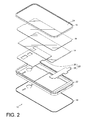
FIG. 2 is an exploded view of the communication device according to the embodiment of the present invention, -
FIG. 3 is a diagram showing arrangement of an antenna of the communication device according to an embodiment of the present invention, -
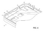
FIG. 4 is a diagram showing arrangement of the antenna at a first position of the communication device according to an embodiment of the present invention, -
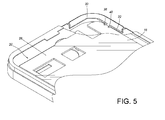
FIG. 5 is a diagram showing arrangement of the antenna at the first position of the communication device (without showing a metal frame) according to the embodiment of the present, -
FIG. 6 is a diagram showing relationship between a metal back cover and a ground terminal of a first circuit block of a printed circuited board according to an embodiment of the present invention, -
FIG. 7 is a diagram showing arrangement of the antenna at a second position of the communication device according to an embodiment of the present invention, -
FIG. 8 is a diagram showing arrangement of the antenna at the second position of the communication device (without showing the metal frame) according to the embodiment of the present,FIG. 9 is an enlarged view of an area A inFIG. 8 , and -
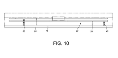
FIG. 10 is a diagram showing relationship between the metal back cover and round terminals of the printed circuited board according to an embodiment of the present invention. -
Fig. 1 andFIG. 2 are diagrams showing acommunication device 10 according to an embodiment of the present invention. Thecommunication device 10 comprises ametal frame 12, adisplay module 14, adisplay panel 16, ametal back cover 18, a printed circuitedboard 20, and amain body 22. Themetal frame 12 substantially is a rectangular frame defining anopening 24, and can be utilized as a front cover of thecommunication device 10. Thedisplay module 14 and thedisplay panel 16 can be separated from each other or integrated together, but the present invention is not limited to the above structure. Thedisplay panel 16 is installed between thedisplay module 14 and themetal frame 12, and corresponding to the opening 24of themetal frame 12. Thedisplay panel 16 is made of glass, but not limited to it. Themetal back cover 18 is substantially rectangular and located at a position corresponding to a bottom of themain body 22, for being utilized as a rear cover of thecommunication device 10. The printedcircuit board 20 is located between themetal frame 12 and themetal back cover 18. Theprinted circuit board 20 comprises afirst circuit block 26 and asecond circuit block 28 electrically connected to thefirst circuit block 26. Themain body 22 is located between themetal frame 12 and themetal back cover 18, for installing thedisplay module 14, thedisplay panel 16 and the printed circuitedboard 20 on themain body 22. In addition, themain body 22 is made of a non-conductive material, such as a plastic material, but not limited to it. -
FIG. 3 is a diagram showing arrangement of an antenna of the communication device according to an embodiment of the present invention.FIG. 4 to FIG. 6 are diagrams showing antenna arrangement of thecommunication device 10 supporting a first communication function, such as a global positioning system (GPS) function. The arrangement inFIG. 4 to FIG. 6 comprises themetal frame 12, thefirst circuit block 26 of theprinted circuit board 20, afirst conductor 30, asecond conductor 32 and themetal back cover 18. Themetal frame 12 has afirst part 34 and asecond part 36 located at a position different from a position of thefirst part 34. In a preferred embodiment, thefirst part 34 and thesecond part 36 of themetal frame 12 are located close to an upper right position of thedisplay panel 16. Thefirst circuit block 26 of theprinted circuit board 20 comprises asignal terminal 38 and aground terminal 40. Thefirst conductor 30 is connected between thefirst part 34 of themetal frame 12 and thesignal terminal 38 of thefirst circuit block 26 of theprint circuit board 20. Thesecond conductor 32 is connected between thesecond part 36 of themetal frame 12 and theground terminal 40 of thefirst circuit block 26 of theprint circuit board 20. When assembling the antenna, themetal back cover 18 contacts theground terminal 40 of thefirst circuit block 26 of the printedcircuit board 20. -
FIG. 7 to FIG. 10 are diagrams showing antenna arrangement of thecommunication device 10 supporting a second communication function, such as a global system for mobile communication (GSM) function. The arrangement inFIG. 7 to FIG. 10 utilizes themetal frame 12 as a common antenna, wherein the arrangement comprises thesecond circuit block 28 of theprinted circuit board 20, athird conductor 42, afourth conductor 44 and asignal line 46. Thesecond circuit block 28 of theprinted circuit board 20 comprises asignal terminal 48 and aground terminal 50. Themetal frame 12 further has athird part 52 and afourth part 54 located at a position different from a position of thethird part 52. In a preferred embodiment, thethird part 52 and thefourth part 54 of themetal frame 12 are located close to a lower right position of thedisplay panel 16. Thethird conductor 42 is connected to thethird part 52 of themetal frame 12, and extended in length to be close to thesecond circuit block 28 of the printedcircuit board 20. Thefourth conductor 44 is connected to a ground surface of thesecond circuit block 28 of theprint circuit board 20 for conducting to theground terminal 50, and at least onecoupling gap 56 is defined between thethird conductor 42 and thefourth conductor 44. Thesignal terminal 48 of thesecond circuit block 28 of the printedcircuit board 20 is electrically connected to thefourth part 54 of themetal frame 12. In an embodiment, thesignal terminal 48 of thesecond circuit block 28 of theprinted circuit board 20 can be electrically connected to thefourth part 54 of themetal frame 12 through thesignal line 46 connecting or contacting thefourth part 54 of themetal frame 12; or, in another embodiment, thesignal terminal 48 of thesecond circuit block 28 of the printedcircuit board 20 can directly connect or contact thefourth part 54 of themetal frame 12, the present invention is not limited to the above. When assembling the antenna, themetal back cover 18 contacts theground terminal 50 of thesecond circuit block 28 of the printedcircuit board 20. - According to the above arrangement, when the
communication device 10 is powered by an external power source, such as a battery, themetal frame 12 can work as a common antenna for the first communication function (GPS) and the second communication function (GSM). The antenna forms an approximate large loop antenna to cooperate with thefirst conductor 30 and thesecond conductor 32 forming a small loop antenna smaller than themetal frame 12, in order to provide required communication capability to thecommunication device 10 through calculation processing of the printedcircuit board 20. On the other hand, thethird conductor 42 and thefourth conductor 44 are pre-arranged to form an open circuit state through the at least onecoupling gap 56, so as to adjust required antenna matching, such as impedance matching, according to requirement. Thesignal terminal 48 of thesecond circuit block 28 of the printedcircuit board 20 is coupled to the ground surface and theground terminal 50 of thesecond circuit block 28 of the printedcircuit board 20 for grounding through the at least onecoupling gap 56, and theground terminal 50 contacts the metal back cover after assembling. - According to the above illustration, the advantages of the present invention is that appearances of the metal back cover and the metal frame are not ruined by design of the antenna, and the present invention can have better appearance in contrast to the prior art, so as to allow the communication device to have great diversity of design.
Claims (5)
- A communication device (10), characterized by:a metal frame (12) defining an opening (24), the metal frame (12) having a first part (34), a second part (36) located at a position different from a position of the first part (34), a third part (52), and a fourth part (54) located at a position different from a position of the third part (52);a display module (14);a display panel (16) installed between the display module (14) and the metal frame (12), and corresponding to the opening (24) of the metal frame (12);a metal back cover (18);a printed circuit board (20), comprising a first circuit block (26) and a second circuit block (28) electrically connected to the first circuit block (26), each of the first and second circuit blocks (26, 28) comprising a signal terminal (38, 48) and a ground terminal (40, 50), wherein the ground terminals (40, 50) contact the metal back cover (18);a main body (22) located between the metal frame (12) and the metal back cover (18), the main body (22) being made of a non-conductive material;a first conductor (30) connected between the first part (34) of the metal frame (12) and the signal terminal (38) of the first circuit block (26) of the print circuit board (20) ;a second conductor (32) connected between the second part (36) of the metal frame (12) and the ground terminal (40) of the first circuit block (26) of the print circuit board (20) ;a third conductor (42) connected to the third part (52) of the metal frame (12); anda fourth conductor (44) connected to the ground terminal (50) of the second circuit block (28) of the print circuit board (20), at least one coupling gap (56) being defined between the third conductor (42) and the fourth conductor (44) ;wherein the signal terminal (48) of the second circuit block (28) of the printed circuit board (20) is electrically connected to the fourth part (44) of the metal frame (12).
- The communication device of claim 1, characterized in that the first part (34) and the second part (36) of the metal frame (12) are located close to an upper right position of the display panel (16).
- The communication device of claim 1 or 2, characterized in that the third part (52) and the fourth part (54) of the metal frame (12) are located close to a lower right position of the display panel (16).
- An antenna of a communication device, characterized by:a metal frame (12) having a first part (34), a second part (36), a third part (52), and a fourth part (54);a metal back cover (18);a printed circuit board (20), comprising a first circuit block (26) and a second circuit block (28) electrically connected to the first circuit block (26), each of the first and second circuit blocks (26, 28) comprising a signal terminal (38, 48) and a ground terminal (40, 50), wherein the ground terminals (40, 50) contact the metal back cover (18);a first conductor (30) connected between the first part (34) of the metal frame (12) and the signal terminal (38) of the first circuit block (26) of the print circuit board (20) ;a second conductor (32) connected between the second part (36) of the metal frame (12) and the ground terminal (40) of the first circuit block (26) of the print circuit board (20) ;a third conductor (42) connected to the third part (52) of the metal frame (12); anda fourth conductor (44) connected to the ground terminal (50) of the second circuit block (28) of the print circuit board (20), at least one coupling gap (56) being defined between the third conductor (42) and the fourth conductor (44) ;wherein the signal terminal (48) of the second circuit block (28) of the printed circuit board (20) is electrically connected to the fourth part (44) of the metal frame (12), and is coupled to the ground terminal (50) of the second circuit block (28) of the printed circuit board (20) through the at least one coupling gap (56).
- The antenna of the communication device of claim 4, characterized in that the third conductor (42) is extended in length to be close to the second circuit block (28) of the printed circuit board (20).
Priority Applications (1)
| Application Number | Priority Date | Filing Date | Title |
|---|---|---|---|
| EP14190198.3A EP3012904B1 (en) | 2014-10-24 | 2014-10-24 | Communication device and antenna thereof |
Applications Claiming Priority (1)
| Application Number | Priority Date | Filing Date | Title |
|---|---|---|---|
| EP14190198.3A EP3012904B1 (en) | 2014-10-24 | 2014-10-24 | Communication device and antenna thereof |
Publications (2)
| Publication Number | Publication Date |
|---|---|
| EP3012904A1 true EP3012904A1 (en) | 2016-04-27 |
| EP3012904B1 EP3012904B1 (en) | 2019-05-08 |
Family
ID=51794778
Family Applications (1)
| Application Number | Title | Priority Date | Filing Date |
|---|---|---|---|
| EP14190198.3A Active EP3012904B1 (en) | 2014-10-24 | 2014-10-24 | Communication device and antenna thereof |
Country Status (1)
| Country | Link |
|---|---|
| EP (1) | EP3012904B1 (en) |
Cited By (3)
| Publication number | Priority date | Publication date | Assignee | Title |
|---|---|---|---|---|
| CN108232428A (en) * | 2018-01-03 | 2018-06-29 | 上海传英信息技术有限公司 | Mobile terminal and its antenna installation method |
| CN110767987A (en) * | 2018-07-27 | 2020-02-07 | 深圳富泰宏精密工业有限公司 | Antenna structure and wireless communication device with same |
| CN119108790A (en) * | 2023-06-08 | 2024-12-10 | Oppo广东移动通信有限公司 | Electronic devices |
Citations (4)
| Publication number | Priority date | Publication date | Assignee | Title |
|---|---|---|---|---|
| US8054231B2 (en) | 2008-05-06 | 2011-11-08 | Samsung Electronics Co., Ltd. | Mobile terminal having metal case and antenna structure |
| US20130135158A1 (en) * | 2011-11-30 | 2013-05-30 | Motorola Solutions, Inc. | Uninterrupted bezel antenna |
| US20140087674A1 (en) * | 2012-09-25 | 2014-03-27 | Htc Corporation | Mobile device |
| US20140132457A1 (en) * | 2012-11-13 | 2014-05-15 | Sony Mobile Communications Ab | Wireless electronic devices with a metal perimeter including a plurality of antennas |
-
2014
- 2014-10-24 EP EP14190198.3A patent/EP3012904B1/en active Active
Patent Citations (4)
| Publication number | Priority date | Publication date | Assignee | Title |
|---|---|---|---|---|
| US8054231B2 (en) | 2008-05-06 | 2011-11-08 | Samsung Electronics Co., Ltd. | Mobile terminal having metal case and antenna structure |
| US20130135158A1 (en) * | 2011-11-30 | 2013-05-30 | Motorola Solutions, Inc. | Uninterrupted bezel antenna |
| US20140087674A1 (en) * | 2012-09-25 | 2014-03-27 | Htc Corporation | Mobile device |
| US20140132457A1 (en) * | 2012-11-13 | 2014-05-15 | Sony Mobile Communications Ab | Wireless electronic devices with a metal perimeter including a plurality of antennas |
Cited By (3)
| Publication number | Priority date | Publication date | Assignee | Title |
|---|---|---|---|---|
| CN108232428A (en) * | 2018-01-03 | 2018-06-29 | 上海传英信息技术有限公司 | Mobile terminal and its antenna installation method |
| CN110767987A (en) * | 2018-07-27 | 2020-02-07 | 深圳富泰宏精密工业有限公司 | Antenna structure and wireless communication device with same |
| CN119108790A (en) * | 2023-06-08 | 2024-12-10 | Oppo广东移动通信有限公司 | Electronic devices |
Also Published As
| Publication number | Publication date |
|---|---|
| EP3012904B1 (en) | 2019-05-08 |
Similar Documents
| Publication | Publication Date | Title |
|---|---|---|
| US9343802B2 (en) | Communication device and antenna thereof | |
| US9203141B1 (en) | Communication device and antenna thereof | |
| CN210805993U (en) | Antenna radiator and electronic device | |
| KR101606145B1 (en) | Antenna device for portable terminal | |
| US10403966B2 (en) | Communication device and antenna assembly thereof | |
| US9331391B2 (en) | Mobile device | |
| MY199346A (en) | Antenna module and electronic device comprising same | |
| US20140354487A1 (en) | Antenna assembly integral with metal housing and electronic device using the antenna assembly | |
| EP3012908B1 (en) | Mobile terminal with novel antenna structure | |
| US20150303551A1 (en) | Communication device antenna | |
| CN112787077A (en) | Antenna radiator and electronic device | |
| US20140313098A1 (en) | Antenna assembly and electronic device using the antenna assembly | |
| US8358777B2 (en) | Wireless telephone having support with built-in antenna | |
| EP3012904B1 (en) | Communication device and antenna thereof | |
| JP2015043572A (en) | Antenna and radio communication device including the same | |
| US10468749B2 (en) | Mobile display terminal | |
| EP2725767B1 (en) | Wireless electronic device with a metal perimeter including a planar user input component | |
| CN108321492A (en) | Electronic equipment | |
| EP2958189B1 (en) | Communication device and antenna thereof | |
| US20150303550A1 (en) | Communication device antenna | |
| US9722299B2 (en) | Antenna assembly, wireless communication device and method of manufacturing same | |
| ZA202401428B (en) | Electronic device comprising antenna | |
| US20150303552A1 (en) | Communication device antenna | |
| JP3195354U (en) | Communication device and communication device antenna | |
| EP1732161A1 (en) | Internal antenna apparatus and mobile communication terminal having same |
Legal Events
| Date | Code | Title | Description |
|---|---|---|---|
| PUAI | Public reference made under article 153(3) epc to a published international application that has entered the european phase |
Free format text: ORIGINAL CODE: 0009012 |
|
| AK | Designated contracting states |
Kind code of ref document: A1 Designated state(s): AL AT BE BG CH CY CZ DE DK EE ES FI FR GB GR HR HU IE IS IT LI LT LU LV MC MK MT NL NO PL PT RO RS SE SI SK SM TR |
|
| AX | Request for extension of the european patent |
Extension state: BA ME |
|
| 17P | Request for examination filed |
Effective date: 20160513 |
|
| RBV | Designated contracting states (corrected) |
Designated state(s): AL AT BE BG CH CY CZ DE DK EE ES FI FR GB GR HR HU IE IS IT LI LT LU LV MC MK MT NL NO PL PT RO RS SE SI SK SM TR |
|
| GRAP | Despatch of communication of intention to grant a patent |
Free format text: ORIGINAL CODE: EPIDOSNIGR1 |
|
| STAA | Information on the status of an ep patent application or granted ep patent |
Free format text: STATUS: GRANT OF PATENT IS INTENDED |
|
| INTG | Intention to grant announced |
Effective date: 20181211 |
|
| RIN1 | Information on inventor provided before grant (corrected) |
Inventor name: LIN, SHU-CHEN Inventor name: LIU, CHUN-TA Inventor name: SU, HSIN-CHENG |
|
| GRAS | Grant fee paid |
Free format text: ORIGINAL CODE: EPIDOSNIGR3 |
|
| GRAA | (expected) grant |
Free format text: ORIGINAL CODE: 0009210 |
|
| STAA | Information on the status of an ep patent application or granted ep patent |
Free format text: STATUS: THE PATENT HAS BEEN GRANTED |
|
| AK | Designated contracting states |
Kind code of ref document: B1 Designated state(s): AL AT BE BG CH CY CZ DE DK EE ES FI FR GB GR HR HU IE IS IT LI LT LU LV MC MK MT NL NO PL PT RO RS SE SI SK SM TR |
|
| REG | Reference to a national code |
Ref country code: GB Ref legal event code: FG4D |
|
| REG | Reference to a national code |
Ref country code: CH Ref legal event code: EP Ref country code: AT Ref legal event code: REF Ref document number: 1131677 Country of ref document: AT Kind code of ref document: T Effective date: 20190515 |
|
| REG | Reference to a national code |
Ref country code: DE Ref legal event code: R096 Ref document number: 602014046175 Country of ref document: DE Ref country code: IE Ref legal event code: FG4D |
|
| REG | Reference to a national code |
Ref country code: NL Ref legal event code: MP Effective date: 20190508 |
|
| REG | Reference to a national code |
Ref country code: LT Ref legal event code: MG4D |
|
| PG25 | Lapsed in a contracting state [announced via postgrant information from national office to epo] |
Ref country code: NO Free format text: LAPSE BECAUSE OF FAILURE TO SUBMIT A TRANSLATION OF THE DESCRIPTION OR TO PAY THE FEE WITHIN THE PRESCRIBED TIME-LIMIT Effective date: 20190808 Ref country code: HR Free format text: LAPSE BECAUSE OF FAILURE TO SUBMIT A TRANSLATION OF THE DESCRIPTION OR TO PAY THE FEE WITHIN THE PRESCRIBED TIME-LIMIT Effective date: 20190508 Ref country code: SE Free format text: LAPSE BECAUSE OF FAILURE TO SUBMIT A TRANSLATION OF THE DESCRIPTION OR TO PAY THE FEE WITHIN THE PRESCRIBED TIME-LIMIT Effective date: 20190508 Ref country code: FI Free format text: LAPSE BECAUSE OF FAILURE TO SUBMIT A TRANSLATION OF THE DESCRIPTION OR TO PAY THE FEE WITHIN THE PRESCRIBED TIME-LIMIT Effective date: 20190508 Ref country code: PT Free format text: LAPSE BECAUSE OF FAILURE TO SUBMIT A TRANSLATION OF THE DESCRIPTION OR TO PAY THE FEE WITHIN THE PRESCRIBED TIME-LIMIT Effective date: 20190908 Ref country code: AL Free format text: LAPSE BECAUSE OF FAILURE TO SUBMIT A TRANSLATION OF THE DESCRIPTION OR TO PAY THE FEE WITHIN THE PRESCRIBED TIME-LIMIT Effective date: 20190508 Ref country code: ES Free format text: LAPSE BECAUSE OF FAILURE TO SUBMIT A TRANSLATION OF THE DESCRIPTION OR TO PAY THE FEE WITHIN THE PRESCRIBED TIME-LIMIT Effective date: 20190508 Ref country code: NL Free format text: LAPSE BECAUSE OF FAILURE TO SUBMIT A TRANSLATION OF THE DESCRIPTION OR TO PAY THE FEE WITHIN THE PRESCRIBED TIME-LIMIT Effective date: 20190508 Ref country code: LT Free format text: LAPSE BECAUSE OF FAILURE TO SUBMIT A TRANSLATION OF THE DESCRIPTION OR TO PAY THE FEE WITHIN THE PRESCRIBED TIME-LIMIT Effective date: 20190508 |
|
| PG25 | Lapsed in a contracting state [announced via postgrant information from national office to epo] |
Ref country code: BG Free format text: LAPSE BECAUSE OF FAILURE TO SUBMIT A TRANSLATION OF THE DESCRIPTION OR TO PAY THE FEE WITHIN THE PRESCRIBED TIME-LIMIT Effective date: 20190808 Ref country code: LV Free format text: LAPSE BECAUSE OF FAILURE TO SUBMIT A TRANSLATION OF THE DESCRIPTION OR TO PAY THE FEE WITHIN THE PRESCRIBED TIME-LIMIT Effective date: 20190508 Ref country code: RS Free format text: LAPSE BECAUSE OF FAILURE TO SUBMIT A TRANSLATION OF THE DESCRIPTION OR TO PAY THE FEE WITHIN THE PRESCRIBED TIME-LIMIT Effective date: 20190508 Ref country code: GR Free format text: LAPSE BECAUSE OF FAILURE TO SUBMIT A TRANSLATION OF THE DESCRIPTION OR TO PAY THE FEE WITHIN THE PRESCRIBED TIME-LIMIT Effective date: 20190809 |
|
| REG | Reference to a national code |
Ref country code: AT Ref legal event code: MK05 Ref document number: 1131677 Country of ref document: AT Kind code of ref document: T Effective date: 20190508 |
|
| REG | Reference to a national code |
Ref country code: DE Ref legal event code: R082 Ref document number: 602014046175 Country of ref document: DE Representative=s name: STRAUS, ALEXANDER, DIPL.-CHEM.UNIV. DR.PHIL., DE Ref country code: DE Ref legal event code: R082 Ref document number: 602014046175 Country of ref document: DE Representative=s name: 2K PATENT- UND RECHTSANWAELTE PARTNERSCHAFT MB, DE |
|
| PG25 | Lapsed in a contracting state [announced via postgrant information from national office to epo] |
Ref country code: RO Free format text: LAPSE BECAUSE OF FAILURE TO SUBMIT A TRANSLATION OF THE DESCRIPTION OR TO PAY THE FEE WITHIN THE PRESCRIBED TIME-LIMIT Effective date: 20190508 Ref country code: SK Free format text: LAPSE BECAUSE OF FAILURE TO SUBMIT A TRANSLATION OF THE DESCRIPTION OR TO PAY THE FEE WITHIN THE PRESCRIBED TIME-LIMIT Effective date: 20190508 Ref country code: AT Free format text: LAPSE BECAUSE OF FAILURE TO SUBMIT A TRANSLATION OF THE DESCRIPTION OR TO PAY THE FEE WITHIN THE PRESCRIBED TIME-LIMIT Effective date: 20190508 Ref country code: EE Free format text: LAPSE BECAUSE OF FAILURE TO SUBMIT A TRANSLATION OF THE DESCRIPTION OR TO PAY THE FEE WITHIN THE PRESCRIBED TIME-LIMIT Effective date: 20190508 Ref country code: DK Free format text: LAPSE BECAUSE OF FAILURE TO SUBMIT A TRANSLATION OF THE DESCRIPTION OR TO PAY THE FEE WITHIN THE PRESCRIBED TIME-LIMIT Effective date: 20190508 Ref country code: CZ Free format text: LAPSE BECAUSE OF FAILURE TO SUBMIT A TRANSLATION OF THE DESCRIPTION OR TO PAY THE FEE WITHIN THE PRESCRIBED TIME-LIMIT Effective date: 20190508 |
|
| REG | Reference to a national code |
Ref country code: DE Ref legal event code: R097 Ref document number: 602014046175 Country of ref document: DE |
|
| PG25 | Lapsed in a contracting state [announced via postgrant information from national office to epo] |
Ref country code: SM Free format text: LAPSE BECAUSE OF FAILURE TO SUBMIT A TRANSLATION OF THE DESCRIPTION OR TO PAY THE FEE WITHIN THE PRESCRIBED TIME-LIMIT Effective date: 20190508 Ref country code: IT Free format text: LAPSE BECAUSE OF FAILURE TO SUBMIT A TRANSLATION OF THE DESCRIPTION OR TO PAY THE FEE WITHIN THE PRESCRIBED TIME-LIMIT Effective date: 20190508 |
|
| PLBE | No opposition filed within time limit |
Free format text: ORIGINAL CODE: 0009261 |
|
| STAA | Information on the status of an ep patent application or granted ep patent |
Free format text: STATUS: NO OPPOSITION FILED WITHIN TIME LIMIT |
|
| PG25 | Lapsed in a contracting state [announced via postgrant information from national office to epo] |
Ref country code: TR Free format text: LAPSE BECAUSE OF FAILURE TO SUBMIT A TRANSLATION OF THE DESCRIPTION OR TO PAY THE FEE WITHIN THE PRESCRIBED TIME-LIMIT Effective date: 20190508 |
|
| 26N | No opposition filed |
Effective date: 20200211 |
|
| PG25 | Lapsed in a contracting state [announced via postgrant information from national office to epo] |
Ref country code: PL Free format text: LAPSE BECAUSE OF FAILURE TO SUBMIT A TRANSLATION OF THE DESCRIPTION OR TO PAY THE FEE WITHIN THE PRESCRIBED TIME-LIMIT Effective date: 20190508 |
|
| PG25 | Lapsed in a contracting state [announced via postgrant information from national office to epo] |
Ref country code: SI Free format text: LAPSE BECAUSE OF FAILURE TO SUBMIT A TRANSLATION OF THE DESCRIPTION OR TO PAY THE FEE WITHIN THE PRESCRIBED TIME-LIMIT Effective date: 20190508 Ref country code: MC Free format text: LAPSE BECAUSE OF FAILURE TO SUBMIT A TRANSLATION OF THE DESCRIPTION OR TO PAY THE FEE WITHIN THE PRESCRIBED TIME-LIMIT Effective date: 20190508 |
|
| REG | Reference to a national code |
Ref country code: CH Ref legal event code: PL |
|
| PG25 | Lapsed in a contracting state [announced via postgrant information from national office to epo] |
Ref country code: LI Free format text: LAPSE BECAUSE OF NON-PAYMENT OF DUE FEES Effective date: 20191031 Ref country code: CH Free format text: LAPSE BECAUSE OF NON-PAYMENT OF DUE FEES Effective date: 20191031 Ref country code: LU Free format text: LAPSE BECAUSE OF NON-PAYMENT OF DUE FEES Effective date: 20191024 |
|
| REG | Reference to a national code |
Ref country code: BE Ref legal event code: MM Effective date: 20191031 |
|
| PG25 | Lapsed in a contracting state [announced via postgrant information from national office to epo] |
Ref country code: BE Free format text: LAPSE BECAUSE OF NON-PAYMENT OF DUE FEES Effective date: 20191031 |
|
| PG25 | Lapsed in a contracting state [announced via postgrant information from national office to epo] |
Ref country code: IE Free format text: LAPSE BECAUSE OF NON-PAYMENT OF DUE FEES Effective date: 20191024 Ref country code: FR Free format text: LAPSE BECAUSE OF NON-PAYMENT OF DUE FEES Effective date: 20191031 |
|
| PG25 | Lapsed in a contracting state [announced via postgrant information from national office to epo] |
Ref country code: CY Free format text: LAPSE BECAUSE OF FAILURE TO SUBMIT A TRANSLATION OF THE DESCRIPTION OR TO PAY THE FEE WITHIN THE PRESCRIBED TIME-LIMIT Effective date: 20190508 |
|
| PG25 | Lapsed in a contracting state [announced via postgrant information from national office to epo] |
Ref country code: IS Free format text: LAPSE BECAUSE OF FAILURE TO SUBMIT A TRANSLATION OF THE DESCRIPTION OR TO PAY THE FEE WITHIN THE PRESCRIBED TIME-LIMIT Effective date: 20190908 |
|
| PG25 | Lapsed in a contracting state [announced via postgrant information from national office to epo] |
Ref country code: MT Free format text: LAPSE BECAUSE OF FAILURE TO SUBMIT A TRANSLATION OF THE DESCRIPTION OR TO PAY THE FEE WITHIN THE PRESCRIBED TIME-LIMIT Effective date: 20190508 Ref country code: HU Free format text: LAPSE BECAUSE OF FAILURE TO SUBMIT A TRANSLATION OF THE DESCRIPTION OR TO PAY THE FEE WITHIN THE PRESCRIBED TIME-LIMIT; INVALID AB INITIO Effective date: 20141024 |
|
| PG25 | Lapsed in a contracting state [announced via postgrant information from national office to epo] |
Ref country code: MK Free format text: LAPSE BECAUSE OF FAILURE TO SUBMIT A TRANSLATION OF THE DESCRIPTION OR TO PAY THE FEE WITHIN THE PRESCRIBED TIME-LIMIT Effective date: 20190508 |
|
| REG | Reference to a national code |
Ref country code: DE Ref legal event code: R082 Ref document number: 602014046175 Country of ref document: DE Representative=s name: STRAUS, ALEXANDER, DIPL.-CHEM.UNIV. DR.PHIL., DE |
|
| PGFP | Annual fee paid to national office [announced via postgrant information from national office to epo] |
Ref country code: GB Payment date: 20250805 Year of fee payment: 12 |
|
| PGFP | Annual fee paid to national office [announced via postgrant information from national office to epo] |
Ref country code: DE Payment date: 20250611 Year of fee payment: 12 |