EP3012718B1 - Touch panel and three-dimensional cover plate thereof - Google Patents
Touch panel and three-dimensional cover plate thereof Download PDFInfo
- Publication number
- EP3012718B1 EP3012718B1 EP15184157.4A EP15184157A EP3012718B1 EP 3012718 B1 EP3012718 B1 EP 3012718B1 EP 15184157 A EP15184157 A EP 15184157A EP 3012718 B1 EP3012718 B1 EP 3012718B1
- Authority
- EP
- European Patent Office
- Prior art keywords
- transparent substrate
- side panel
- cover plate
- substrate
- layer
- Prior art date
- Legal status (The legal status is an assumption and is not a legal conclusion. Google has not performed a legal analysis and makes no representation as to the accuracy of the status listed.)
- Not-in-force
Links
Images

Classifications
-
- G—PHYSICS
- G06—COMPUTING OR CALCULATING; COUNTING
- G06F—ELECTRIC DIGITAL DATA PROCESSING
- G06F3/00—Input arrangements for transferring data to be processed into a form capable of being handled by the computer; Output arrangements for transferring data from processing unit to output unit, e.g. interface arrangements
- G06F3/01—Input arrangements or combined input and output arrangements for interaction between user and computer
- G06F3/03—Arrangements for converting the position or the displacement of a member into a coded form
- G06F3/041—Digitisers, e.g. for touch screens or touch pads, characterised by the transducing means
-
- B—PERFORMING OPERATIONS; TRANSPORTING
- B32—LAYERED PRODUCTS
- B32B—LAYERED PRODUCTS, i.e. PRODUCTS BUILT-UP OF STRATA OF FLAT OR NON-FLAT, e.g. CELLULAR OR HONEYCOMB, FORM
- B32B17/00—Layered products essentially comprising sheet glass, or glass, slag, or like fibres
- B32B17/06—Layered products essentially comprising sheet glass, or glass, slag, or like fibres comprising glass as the main or only constituent of a layer, next to another layer of a specific material
-
- B—PERFORMING OPERATIONS; TRANSPORTING
- B32—LAYERED PRODUCTS
- B32B—LAYERED PRODUCTS, i.e. PRODUCTS BUILT-UP OF STRATA OF FLAT OR NON-FLAT, e.g. CELLULAR OR HONEYCOMB, FORM
- B32B9/00—Layered products comprising a layer of a particular substance not covered by groups B32B11/00 - B32B29/00
- B32B9/005—Layered products comprising a layer of a particular substance not covered by groups B32B11/00 - B32B29/00 comprising one layer of ceramic material, e.g. porcelain, ceramic tile
-
- B—PERFORMING OPERATIONS; TRANSPORTING
- B32—LAYERED PRODUCTS
- B32B—LAYERED PRODUCTS, i.e. PRODUCTS BUILT-UP OF STRATA OF FLAT OR NON-FLAT, e.g. CELLULAR OR HONEYCOMB, FORM
- B32B9/00—Layered products comprising a layer of a particular substance not covered by groups B32B11/00 - B32B29/00
- B32B9/04—Layered products comprising a layer of a particular substance not covered by groups B32B11/00 - B32B29/00 comprising such particular substance as the main or only constituent of a layer, which is next to another layer of the same or of a different material
-
- G—PHYSICS
- G06—COMPUTING OR CALCULATING; COUNTING
- G06F—ELECTRIC DIGITAL DATA PROCESSING
- G06F3/00—Input arrangements for transferring data to be processed into a form capable of being handled by the computer; Output arrangements for transferring data from processing unit to output unit, e.g. interface arrangements
- G06F3/01—Input arrangements or combined input and output arrangements for interaction between user and computer
- G06F3/03—Arrangements for converting the position or the displacement of a member into a coded form
- G06F3/041—Digitisers, e.g. for touch screens or touch pads, characterised by the transducing means
- G06F3/044—Digitisers, e.g. for touch screens or touch pads, characterised by the transducing means by capacitive means
- G06F3/0443—Digitisers, e.g. for touch screens or touch pads, characterised by the transducing means by capacitive means using a single layer of sensing electrodes
-
- B—PERFORMING OPERATIONS; TRANSPORTING
- B32—LAYERED PRODUCTS
- B32B—LAYERED PRODUCTS, i.e. PRODUCTS BUILT-UP OF STRATA OF FLAT OR NON-FLAT, e.g. CELLULAR OR HONEYCOMB, FORM
- B32B2307/00—Properties of the layers or laminate
- B32B2307/40—Properties of the layers or laminate having particular optical properties
- B32B2307/412—Transparent
-
- B—PERFORMING OPERATIONS; TRANSPORTING
- B32—LAYERED PRODUCTS
- B32B—LAYERED PRODUCTS, i.e. PRODUCTS BUILT-UP OF STRATA OF FLAT OR NON-FLAT, e.g. CELLULAR OR HONEYCOMB, FORM
- B32B2457/00—Electrical equipment
- B32B2457/20—Displays, e.g. liquid crystal displays, plasma displays
- B32B2457/208—Touch screens
-
- G—PHYSICS
- G06—COMPUTING OR CALCULATING; COUNTING
- G06F—ELECTRIC DIGITAL DATA PROCESSING
- G06F2203/00—Indexing scheme relating to G06F3/00 - G06F3/048
- G06F2203/041—Indexing scheme relating to G06F3/041 - G06F3/045
- G06F2203/04103—Manufacturing, i.e. details related to manufacturing processes specially suited for touch sensitive devices
Definitions
- the present disclosure relates to touch panels. More particularly, the present disclosure relates to touch panels and three-dimensional cover plates thereof.
- Touch panels are widely used in display screens of electronic products, such as cellular phones, cameras and tablets, to enhance convenience of control and signal input.
- electronic products such as cellular phones, cameras and tablets
- touch panel For example, general smart phones and tablet computers include a touch panel, and users input signals through the touch panel directly, such as into a handwriting recognition system.
- a cover glass for electronic devices is known, which is manufactured by stacking two sheets above each other and by a subsequent dicing step.
- a mobile electronic device with a composite cover plate comprising sapphire and glass is known.
- US 2010/0237458 A1 discloses a substrate with a bonding layer of silicon oxide with a thickness of less than or equal to 500 nm for semiconductor devices, such as for electroluminescence and liquid crystal display devices, for field effect transistors and for microprocessors.
- US 2014/0273281 A1 relates to a method for forming biochips for improved thermal budget.
- the present invention relates to a method of manufacturing a three-dimensional cover plate according to claim 1.
- the dependent claims relate to preferred embodiments.
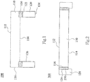
- Fig. 1 illustrates a cross-sectional view of a three-dimensional cover plate 100 according to an example helpful for understanding the present disclosure.
- the three-dimensional cover plate Ioo includes a transparent substrate 110 and a side panel 120.
- the side panel 120 is bonded to a part of the transparent substrate 110, and a binding layer 130 is disposed between the transparent substrate 110 and the side panel 120 to bond the transparent substrate 110 and the side panel 120. Bonding can indicate that a bond is formed between the transparent substrate 110 and the side panel 120, so as to achieve a stable and strong composite of the transparent substrate 110 and the side panel 120.
- the three-dimensional cover plate 100 includes one side panel 120, and this side panel 120 is disposed at one edge of a lower surface 114 of the transparent substrate 110. In various examples, the three-dimensional cover plate 100 includes a plurality of side panels 120, and these side panels 120 are disposed at edges of the lower surface 114 and surround a periphery of the lower surface 114.
- the transparent substrate 110 includes an upper surface 112 and a lower surface 114
- the side panel 120 also includes an upper surface 122 and a lower surface 124.
- the transparent substrate 110 and the side panel 120 are transparent planar plate, such as glass or sapphire.
- the glass is preferably selected from glass for touching (float glass) or aluminate glass.
- a surface treatment is performed on the surfaces predetermined for bonding.
- the surface treatment is performed on the upper surface 122 of the side panel 120 and the lower surface 114 of the transparent substrate 1 10, to make the upper surface 122 and the lower surface 114 hydrophilic and have valence bonds.
- the hydrophilic upper surface 122 of the side panel 120 and the hydrophilic lower surface 114 of the transparent substrate 110 adsorb hydroxyl groups, which react with silicon in the glass to form silanol bonds (Si-OH). Similarly, the hydroxyl groups also react with aluminum in the sapphire to form aluminum alcohol bonds (AI-OH).
- the upper surface 122 of the side panel 120 and the lower surface 114 of the transparent substrate 110 are overlapped to form a contact surface therebetween. Then, an annealing process is performed on the side panel 120 and the transparent substrate 110 to polymerize silanol bonds and aluminium alcohol bonds at high temperature, and the binding layer 130 is formed with aluminum-oxygen-silicon bonds (AI-o-Si), silicon-oxygen-silicon bonds (Si-o-Si), or aluminum-oxygen-aluminum bonds (AI-o-AI) therein to achieve a stable composite of the side panel 120 and the transparent substrate 110.
- a thickness of the binding layer 130 is very thin, which is less than or equal to about 10 nm.
- the upper surface 122 of side panel 120 is bonded to a periphery of the lower surface 114 of the transparent substrate 110. Furthermore, the transparent substrate 110 has a side surface 116 adjacent to the lower surface 114 and the upper surface 112, and the side panel 120 has a side surface 126 adjacent to the upper surface 122 and lower surface 124. The side surface 126 of the side panel 120 is flush with the side surface 116 of the transparent substrate 110, and the three-dimensional cover plate 100 with integrated seamless connection is formed.
- the transparent substrate has a thickness in a range from about 0.3 mm to about 2.0 mm.
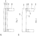
- Fig. 2 illustrates a cross-sectional view of a three-dimensional cover plate 200 according to various embodiments of the present disclosure.
- the present disclosure is not limited to bonding the upper surface 122 of the side panel 120 and the lower surface 114 of the transparent substrate 110.
- the side surface 126 of the side panel 120 is bonded to the side surface II 6o f the transparent substrate 110 to form a binding layer 230 between the side surface 126 of the side panel 120 and the side surface 116 of the transparent substrate 110.
- the binding layer 230 includes aluminum-oxygen-silicon bonds (AI-o-Si), silicon-oxygen-silicon bonds (Si-o-Si), or aluminum-oxygen-aluminum bonds (AI-o-AI).
- the side surface 126 of the side panel 120 is bonded to the side surface 116 of the transparent substrate 110, and the upper surface 112 of the transparent substrate 110 is flush with the upper surface 122 of the side panel 120 to form a three-dimensional cover plate 200 with integrated seamless connection.
- the transparent substrate 110 and the side panel 120 are bonded with an angle of 90 degrees between the lower surface 114 of the transparent substrate 110 and the side surface 126 of the side panel 120, as shown in the three-dimensional cover plate 100 and 200 in Fig. 1 and Fig. 2 , no limitation is made thereto. Other cases in which the composite of the transparent substrate 110 and side panel 120 is formed at an angle in a range from 100 to 180 degrees, are also contemplated herein.
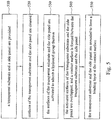
- Fig. 3 illustrates a cross-sectional view of a three-dimensional cover plate 300 according to an example helpful for understanding the present disclosure.
- the three-dimensional cover plate 300 includes a transparent composite substrate 310, which includes a glass substrate 312, a sapphire substrate 316 and a second binding layer 314.
- the second binding layer 314 is disposed between the glass substrate 312 and the sapphire substrate 316 to stably bond the two, and the second binding layer 314 includes aluminum-oxygen-silicon bonds (AI-o-Si).
- a side panel 320 is stably bonded to the glass substrate 312 by a first binding layer 330, which includes aluminum-oxygen-silicon bonds (AI-o-Si) or silicon-oxygen-silicon bonds (Si-o-Si).
- the side panel 320 is stably bonded to the sapphire substrate 316 by the first binding layer 330, which includes aluminum-oxygen-silicon bonds (AI-o-Si) or aluminum-oxygen- aluminum bonds (AI-o-AI).
- the glass substrate 312 may be, for example, a substrate through chemical strengthening, which has better strength to improve the sapphire substrate 316 with thinner thickness and lower compression resistance.
- the sapphire substrate 316 acts as a touching surface, and one surface of the glass substrate 312 away from the sapphire substrate 316 is combined with other touch or display devices, so as to improve the scratch resistance and the compression resistance of the three-dimensional cover plate 300.
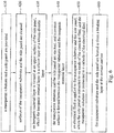
- Fig. 4 illustrates a cross-sectional view of a three-dimensional cover plate 400 according to an example helpful for understanding the present disclosure.
- the three-dimensional cover plate 400 includes a transparent substrate 410, a side panel 420, and a binding layer 430 disposed between the transparent substrate 410 and the side panel 420, so as to bond the transparent substrate 410 and the side panel 420.
- the three-dimensional cover plate 400 further includes an inorganic material layer 440 disposed between the binding layer 430 and the side panel 420.
- the inorganic material layer 410 is a silicon layer or a silicon dioxide layer to achieve higher bonding strength between the transparent substrate 410 and the side panel 420.
- the transparent substrate 410 and the side panel 420 are independently formed of glass or sapphire.
- the inorganic material layer 440 is preferably formed on a surface of the sapphire plate.
- the transparent substrate may be the transparent composite substrate 310 shown in Fig. 3 . It is worth noting that the side panel 420 is bonded to the glass substrate 312 of the transparent composite substrate 310, and the binding layer 430 includes silicon-oxygen-silicon bonds (Si-o-Si).
- Fig. 5 is a flow chart illustrating a method of manufacturing a three-dimensional cover plate, according to an example helpful for understanding the present disclosure. The method can be used in accordance with manufacture of the three-dimensional cover plate 100 shown in Fig. I , which starts with step 510, in which a transparent substrate 110 and a side panel 120 are provided.
- the surfaces of the transparent substrate 110 and the side panel 120 are cleaned. Because the cleanness of the bonding surfaces influence the bonding strength, dust and particles on the surfaces of the transparent substrate 110 and the side panel 120 are cleaned away with water, alcohol, acetone, or a combination thereof before bonding. In addition, the flatness of the bonding surfaces also influences the bonding strength. The surfaces of the transparent substrate 110 and the side panel 120 are polished before cleaning, so as to obtain flat and smooth surfaces.
- the surfaces of the transparent substrate 110 and the side panel 120 are activated to adsorb a hydroxyl group thereon.
- a plasma gas such as nitrogen gas, argon gas, or neon gas, generates ions or neutral atoms at high temperature and high energy, and these ions or neutral atoms physically impact the surfaces of transparent substrate 110 and the side panel 120. Therefore, the surfaces predetermined for bonding adsorb the hydroxyl groups thereon.
- some unstable oxygen atoms are on the surfaces or in vivo of the transparent substrate 110 and the side panel 120. Under certain conditions, these unstable oxygen atoms are activated to leave silicon atoms and aluminum atoms, and dangling bonds are formed at the surfaces.
- Fig. 1 some unstable oxygen atoms are on the surfaces or in vivo of the transparent substrate 110 and the side panel 120. Under certain conditions, these unstable oxygen atoms are activated to leave silicon atoms and aluminum atoms, and dangling bonds are formed at the surfaces.
- the lower surface 114 of the transparent substrate 11 0 and the upper surface 122 of the side panel 120 are activated by the plasma gas to form hydrophilic lower surface 114 and hydrophilic upper surface 122.
- the hydrophilic lower surface 114 of the transparent substrate 110 and the hydrophilic upper surface 122 of the side panel 120 are able to adsorb hydroxyl groups, so as to form the silanol bonds (Si-OH) and the aluminum alcohol bonds (AI-OH).
- the plasma gas is a low-temperature plasma gas.
- the plasma gas is in a vacuum environment to increase efficiency of the process.
- the activated surfaces of the transparent substrate 110 and the side panel 120 are overlapped, and a contact surface is formed between the transparent substrate 110 and the side panel 120.
- the activated lower surface 114 of the transparent substrate 110 and the activated upper surface 122 of the side panel 120 are overlapped to form the contact surface between the transparent substrate 110 and the side panel 120.
- the lower surface 1 14 and the upper surface 122 are hydrophilic, water molecules are easily adsorbed thereon, and a hydrogen bonding bridge is formed at the contact surface to attract the lower surface 114 to the upper surface 122.
- the bonding strength of the hydrogen bonding bridge is stronger than a van der Waals force between atoms, so an initial bonding is much easier to be achieved.
- the transparent substrate 110 and the side panel 120 are annealed to form a binding layer 130 at the contact surface.
- the transparent substrate 110 and the side panel 120 are heated in an atmosphere furnace to perform an annealing process.
- the hydrogen bonds between the lower surface 114 and the upper surface 122 disappear, and oxygen bonds (-0-0- or -0-) are formed to shorten the space between the atoms at the contact surface.
- the silanol bonds or the aluminum alcohol bonds at the lower surface 114 of the transparent substrate 110 are polymerized with the silanol bonds or the aluminum alcohol bonds at the upper surface 122 of the side panel 120, and the binding layer 130 having silicon-oxygen-silicon bonds, aluminum-oxygen-silicon bonds or aluminum-oxygen-aluminum bonds is formed at the contact surface to achieve a stable composite of the transparent substrate 110 and the side panel 120.
- the flow chart shown in Fig. 5 is not limited to manufacture of the three-dimensional cover plates 100, 200, 300 shown in Fig. 1 to Fig. 3 , but could be also used to manufacture the three-dimensional cover plate shown in Fig. 4 .
- the inorganic material layer 440 is coated on the upper surface 422 of the side panel 420, and steps of cleaning, activating, stacking and annealing are performed to form the binding layer 430 between the transparent substrate 410 and the side panel 420.
- the transparent substrate 410 is preferably formed of glass.
- the binding layer 430 includes silicon-oxygen-silicon bonds (Si-o-Si) to achieve a stable composite of the transparent substrate 410 and the side panel 420 though the inorganic material layer 440.
- Fig. 6 is a flow chart illustrating a method of manufacturing a three-dimensional cover plate, according to various embodiments of the present disclosure. The method starts with step 610, in which a transparent substrate 410 and a side panel 420 are provided to manufacture the three-dimensional cover plate 400 shown in Fig. 4 .
- the surfaces of the transparent substrate 410 and the side panel 420 are cleaned. Because the cleanness of the bonding surfaces will influence the bonding strength, dust and particles on the surfaces of the transparent substrate 410 and the side panel 420 are cleaned with water, alcohol, acetone, or combination thereof before bonding. In addition, the flatness of the bonding surfaces also influences the bonding strength. The surfaces of the transparent substrate 410 and the side panel 420 are polished before cleaning, so as to obtain flat and smooth surfaces.
- an inorganic material layer 440 is formed at the upper surface 422 of the side panel 420.
- the inorganic material layer 440 is a silicon layer or a silicon dioxide layer. As shown in Fig. 4 , the inorganic material layer 440 is formed on the upper surface 422 of the side panel 420 and in contact with the side panel 420. In some embodiments, the inorganic material layer 440 is formed by coating. In some embodiments, the inorganic material layer 440 is a silicon layer or a silicon dioxide layer having a thickness in a range from about 1 um to about 10 um.
- the transparent substrate 410 and the side panel 420 are stacked, and a contact surface is formed between the transparent substrate 410 and the side panel 420.
- the transparent substrate 410 is stacked with the side panel 420 having the inorganic material layer 440 on the upper surface 422 to form the contact surface between the inorganic material layer 440 and the transparent substrate 110.
- an electrical field is applied to the transparent substrate 410 and the side panel 420.
- the side panel 420 is connected to an anode of the electrical field, and the transparent substrate 410 is connected to a cathode of the electrical field.
- the transparent substrate 410 and the side panel 420 are placed in a bonding machine for bonding.
- the bonding machine generates the electrical field applied to the transparent substrate 410 and the side panel 420.
- the lower surface 424 of the side panel 420 is connected to the anode of the electrical field, and the upper surface 412 of the transparent substrate 410 is connected to the cathode of the electrical field.
- a huge current pulse is generated. When the current pulse is gradually decreased to zero, the bonding process is completed.
- the electrical field has a voltage in a range from about 300 V to about 800 V, preferably 360V.
- the electrical field is applied to cause ions in the transparent substrate 410 to migrate, so that the transparent substrate 410 is formed of glass.
- the transparent substrate 410 may be the transparent composite substrate 310 shown in Fig. 3 , and the side panel 420 is bonded to the glass substrate 312 of the transparent composite substrate 310.
- the alkali metal ions in the transparent substrate 410 migrate toward the cathode and aggregate at the upper surface 412 of the transparent substrate 410. Therefore, a depletion region having negative charges is formed at the upper surface 412 of the transparent substrate 410 adjacent to the inorganic material layer 440. A huge electrostatic attraction force is formed between the depletion region and the inorganic material layer 440 having positive charges to make the transparent substrate 410 bond stably to the side panel 420.
- the transparent substrate 410 and the side panel 420 are heated to form the binding layer 430 at the contact surface.
- the bonding process is performed at high temperature, about 200°C to 400°C, to assist the electrostatic attraction force, and the bonding strength is further increased.
- oxygen ions remain at the lower surface 414 of the transparent substrate 410 due to the migration of the alkali metal ions. These oxygen ions react with silicon inside the inorganic material layer 440 at high temperature to form stable silicon-oxygen-silicon bonds (Si-0-Si) in the binding layer 430 to achieve a stable composite of the transparent substrate 410 and the side panel 420.
- Fig. 7 illustrates a cross-sectional view of a touch panel 1000 according to an example helpful for understanding the present disclosure.
- the touch panel 1000 includes a transparent substrate 1100 and a side panel 1200 at a lower surface of the transparent substrate 1100.
- a first binding layer 1300 is disposed between the transparent substrate 1100 and the side panel 1200 to bond the two with a bond therebetween.
- the positional relationship between the transparent substrate 1100 and the side panel 1200 is similar to the configuration shown in Fig. 1 , but not limited thereto.
- the side panel 1200 is at a side surface of the transparent substrate 1100, which is similar to the configuration shown in Fig. 2 , and the two are bonded through the first binding layer 1300.
- an anti-reflective film 1400 is disposed on an upper surface the transparent substrate 1100.
- the anti-reflective film 1400 may be a single-layer or multi-layer transparent film having anti-reflective or anti-glare functionality.
- a touch sensing device 1500 is disposed below the lower surface of the transparent substrate 1100.
- the touch sensing device 1500 and the anti-reflective film 1400 are respectively at two opposite sides of the transparent substrate 1100.
- the touch sensing device 1500 includes a sensing electrode layer 1520 and a wire layer 1540.
- the sensing electrode layer 1520 is a sensing electrode directly formed at the lower surface of the transparent substrate 1100.
- the sensing electrode layer 1520 is a sensing electrode film or a sensing electrode substrate adhered to the lower surface of the transparent substrate 1100.
- the wire layer 1540 is disposed at the side surface of the side panel 1200 adjacent to the lower surface of the transparent substrate 1100, and the sensing electrode layer 1520 is the sensing electrode film electrically connecting to the wire layer 1540.
- the sensing electrode layer 1520 is formed of transparent conductive material, such as indium tin oxide (ITO), indium zinc oxide (IZO), cadmium tin oxide (CTO), aluminum zinc oxide (AZO), indium tin zinc oxide (ITZO), graphene, Ag nanowire, or carbon nanotubes (CNT), but not limited thereto.
- the wire layer 1540 is formed of transparent conductive material the same as the sensing electrode layer 1520, or opaque conductive material, such as Ag, Cu, Mo, Al, or other suitable metals or alloys.
- the sensing electrode layer 1520 and the wire layer 1540 are formed by printing and laser etching, or sputtering and photolithography etching.
- the sensing electrode layer 1520 generates signals when sensing touching, and the wire layer 1540 transfers the signals to a processor to calculate the location of touching.
- a plurality of touch functional devices 1600 are also disposed at the side surface of the side panel 1200 adjacent to the lower surface of the transparent substrate 1100, and these touch functional devices 1600 are electrically connected to the wire layer 1540.
- These touch functional devices 1600 have functionality of adjusting volume, photographing, and powering on/off, but not limited thereto.
- the transparent substrate 110 is a transparent composite substrate including a sapphire substrate, a glass substrate and a second binding layer to bond the sapphire substrate and the glass substrate with a bond therebetween.
- the sapphire substrate acts as a touching surface to make the touch panel 1000 have the scratch resistance of the sapphire substrate and the strength of the glass substrate. Specifically, users operate programs and give instructions by touching patterns shown on the sapphire substrate.
- the sapphire is directly bonded to the glass substrate to form the second binding layer having silicon-oxygen-aluminum bonds at a contact surface.
- the inorganic material layer is coated on the sapphire substrate, and then the sapphire substrate is bonded to the glass substrate to form the second binding layer having silicon-oxygen-silicon bonds between the glass substrate and the inorganic material layer.
- the transparent substrate and the side panel in above embodiments and figures are illustrated by a planar substrate, but not limited thereto.
- the transparent substrate and the side panel may be 2.5D or 3D substrate, which means that the upper surface of the transparent substrate or a surface combined by the upper surface and the side surface may be a curve surface.
- the side surface of the side panel or a surface combined by the side surface and the lower surface may be a curved surface.
- the touch panel using the three-dimensional cover plate increases diversification of the touch mode. Users could not only use the common planar touch panel, but also perform touch operation at the sides of the touch panel.
- the three-dimensional cover plate has advantages of high dimensional accuracy and flat surface, and pitting particles are not formed during the manufacturing, so as to form the three-dimensional cover plate with integrated seamless connection. Therefore, it is not necessary to remove these pitting particles in excessive subsequent process.
- the temperature of the process is much lower to decrease risk, and the process also reduces costs to achieve the target of mass production.
- the three-dimensional cover plate of the present disclosure has high bonding strength to maintain stable and solid bonding at high temperature and pressure, and thereby being widely applied to the touch device.
Landscapes
- Engineering & Computer Science (AREA)
- General Engineering & Computer Science (AREA)
- Theoretical Computer Science (AREA)
- Human Computer Interaction (AREA)
- Physics & Mathematics (AREA)
- General Physics & Mathematics (AREA)
- Ceramic Engineering (AREA)
- Chemical & Material Sciences (AREA)
- Laminated Bodies (AREA)
- Position Input By Displaying (AREA)
Description
- This application claims priority to Chinese Application
CN 10 55 28 101 A, filed October 21, 2014 . - The present disclosure relates to touch panels. More particularly, the present disclosure relates to touch panels and three-dimensional cover plates thereof.
- Touch panels are widely used in display screens of electronic products, such as cellular phones, cameras and tablets, to enhance convenience of control and signal input. For example, general smart phones and tablet computers include a touch panel, and users input signals through the touch panel directly, such as into a handwriting recognition system.
- However, glass and sapphire are commonly used in these products to manufacture a cover plate of the planar touch panel, but there is no touch functionality at sides of the products. Generally, buttons or switches are disposed at the sides of the products for operation. Although current technology allows manufacture of three-dimensional glass cover plates by a heat bending process, dimensional accuracy of the three-dimensional glass cover plate is hard to control. In addition, particles that form pits remain on surfaces of the glass cover plate, and a subsequent process is necessary to polish the surfaces to achieve product specifications. The heat bending process further requires high temperature to manufacture the three-dimensional glass cover plate, which increases cost and risk in the manufacturing process.
- From
US 2013/0071601 a cover glass for electronic devices is known, which is manufactured by stacking two sheets above each other and by a subsequent dicing step. FromUS 2014/0133074 A1 a mobile electronic device with a composite cover plate comprising sapphire and glass is known.US 2010/0237458 A1 discloses a substrate with a bonding layer of silicon oxide with a thickness of less than or equal to 500 nm for semiconductor devices, such as for electroluminescence and liquid crystal display devices, for field effect transistors and for microprocessors.US 2014/0273281 A1 relates to a method for forming biochips for improved thermal budget. - The present invention relates to a method of manufacturing a three-dimensional cover plate according to claim 1. The dependent claims relate to preferred embodiments.
- The invention can be more fully understood by reading the following detailed description of the embodiment, with reference made to the accompanying drawings as follows:
-
Fig. 1 illustrates a cross-sectional view of a three-dimensional cover plate according to an example helpful for understanding the present disclosure. -
Fig. 2 illustrates a cross-sectional view of a three-dimensional cover plate according to various embodiments of the present disclosure. -
Fig. 3 illustrates a cross-sectional view of a three-dimensional cover plate according to an example helpful for understanding the present disclosure. -
Fig. 4 illustrates a cross-sectional view of a three-dimensional cover plate according to an example helpful for understanding the present disclosure. -
Fig. 5 is a flow chart illustrating a method of manufacturing a three-dimensional cover plate, according to an example helpful for understanding the present disclosure. -
Fig. 6 is a flow chart illustrating a method of manufacturing a three-dimensional cover plate, according to various embodiments of the present disclosure. -
Fig. 7 is a cross-sectional view of a touch panel according to an example helpful for understanding the present disclosure. - The following disclosure provides many different embodiments, or examples not covered by the claims, for implementing different features of the provided subject matter. Specific examples of components and arrangements are described below to simplify the present disclosure. These are, of course, merely examples and are not intended to be limiting. In addition, the present disclosure may repeat reference numerals and/or letters in the various examples. This repetition is for the purpose of simplicity and clarity and does not in itself dictate a relationship between the various embodiments and/or configurations discussed.
-
Fig. 1 illustrates a cross-sectional view of a three-dimensional cover plate 100 according to an example helpful for understanding the present disclosure. As shown inFig. 1 , the three-dimensional cover plate Ioo includes atransparent substrate 110 and aside panel 120. Theside panel 120 is bonded to a part of thetransparent substrate 110, and abinding layer 130 is disposed between thetransparent substrate 110 and theside panel 120 to bond thetransparent substrate 110 and theside panel 120. Bonding can indicate that a bond is formed between thetransparent substrate 110 and theside panel 120, so as to achieve a stable and strong composite of thetransparent substrate 110 and theside panel 120. In some examples, the three-dimensional cover plate 100 includes oneside panel 120, and thisside panel 120 is disposed at one edge of alower surface 114 of thetransparent substrate 110. In various examples, the three-dimensional cover plate 100 includes a plurality ofside panels 120, and theseside panels 120 are disposed at edges of thelower surface 114 and surround a periphery of thelower surface 114. - Specifically, the
transparent substrate 110 includes anupper surface 112 and alower surface 114, and theside panel 120 also includes anupper surface 122 and alower surface 124. Thetransparent substrate 110 and theside panel 120 are transparent planar plate, such as glass or sapphire. The glass is preferably selected from glass for touching (float glass) or aluminate glass. - During the bonding process, a surface treatment is performed on the surfaces predetermined for bonding. In some embodiments, the surface treatment is performed on the
upper surface 122 of theside panel 120 and thelower surface 114 of the transparent substrate 1 10, to make theupper surface 122 and thelower surface 114 hydrophilic and have valence bonds. After the surface treatment, the hydrophilicupper surface 122 of theside panel 120 and the hydrophiliclower surface 114 of thetransparent substrate 110 adsorb hydroxyl groups, which react with silicon in the glass to form silanol bonds (Si-OH). Similarly, the hydroxyl groups also react with aluminum in the sapphire to form aluminum alcohol bonds (AI-OH). - The
upper surface 122 of theside panel 120 and thelower surface 114 of thetransparent substrate 110 are overlapped to form a contact surface therebetween. Then, an annealing process is performed on theside panel 120 and thetransparent substrate 110 to polymerize silanol bonds and aluminium alcohol bonds at high temperature, and thebinding layer 130 is formed with aluminum-oxygen-silicon bonds (AI-o-Si), silicon-oxygen-silicon bonds (Si-o-Si), or aluminum-oxygen-aluminum bonds (AI-o-AI) therein to achieve a stable composite of theside panel 120 and thetransparent substrate 110. A thickness of thebinding layer 130 is very thin, which is less than or equal to about 10 nm. - In some examples, the
upper surface 122 ofside panel 120 is bonded to a periphery of thelower surface 114 of thetransparent substrate 110. Furthermore, thetransparent substrate 110 has aside surface 116 adjacent to thelower surface 114 and theupper surface 112, and theside panel 120 has aside surface 126 adjacent to theupper surface 122 andlower surface 124. Theside surface 126 of theside panel 120 is flush with theside surface 116 of thetransparent substrate 110, and the three-dimensional cover plate 100 with integrated seamless connection is formed. - In some examples, the transparent substrate has a thickness in a range from about 0.3 mm to about 2.0 mm.
-
Fig. 2 illustrates a cross-sectional view of a three-dimensional cover plate 200 according to various embodiments of the present disclosure. Please note that the present disclosure is not limited to bonding theupper surface 122 of theside panel 120 and thelower surface 114 of thetransparent substrate 110. As shown inFig. 2 , in some embodiments, theside surface 126 of theside panel 120 is bonded to the side surface II 6o f thetransparent substrate 110 to form abinding layer 230 between theside surface 126 of theside panel 120 and theside surface 116 of thetransparent substrate 110. Thebinding layer 230 includes aluminum-oxygen-silicon bonds (AI-o-Si), silicon-oxygen-silicon bonds (Si-o-Si), or aluminum-oxygen-aluminum bonds (AI-o-AI). - The
side surface 126 of theside panel 120 is bonded to theside surface 116 of thetransparent substrate 110, and theupper surface 112 of thetransparent substrate 110 is flush with theupper surface 122 of theside panel 120 to form a three-dimensional cover plate 200 with integrated seamless connection. - Although the
transparent substrate 110 and theside panel 120 are bonded with an angle of 90 degrees between thelower surface 114 of thetransparent substrate 110 and theside surface 126 of theside panel 120, as shown in the three-dimensional cover plate Fig. 1 and Fig. 2 , no limitation is made thereto. Other cases in which the composite of thetransparent substrate 110 andside panel 120 is formed at an angle in a range from 100 to 180 degrees, are also contemplated herein. -
Fig. 3 illustrates a cross-sectional view of a three-dimensional cover plate 300 according to an example helpful for understanding the present disclosure. As shown inFig. 3 , the three-dimensional cover plate 300 includes atransparent composite substrate 310, which includes aglass substrate 312, asapphire substrate 316 and a secondbinding layer 314. The second bindinglayer 314 is disposed between theglass substrate 312 and thesapphire substrate 316 to stably bond the two, and the second bindinglayer 314 includes aluminum-oxygen-silicon bonds (AI-o-Si). Aside panel 320 is stably bonded to theglass substrate 312 by a first bindinglayer 330, which includes aluminum-oxygen-silicon bonds (AI-o-Si) or silicon-oxygen-silicon bonds (Si-o-Si). In some examples, theside panel 320 is stably bonded to thesapphire substrate 316 by the firstbinding layer 330, which includes aluminum-oxygen-silicon bonds (AI-o-Si) or aluminum-oxygen- aluminum bonds (AI-o-AI). Theglass substrate 312 may be, for example, a substrate through chemical strengthening, which has better strength to improve thesapphire substrate 316 with thinner thickness and lower compression resistance. Preferably, thesapphire substrate 316 acts as a touching surface, and one surface of theglass substrate 312 away from thesapphire substrate 316 is combined with other touch or display devices, so as to improve the scratch resistance and the compression resistance of the three-dimensional cover plate 300. -
Fig. 4 illustrates a cross-sectional view of a three-dimensional cover plate 400 according to an example helpful for understanding the present disclosure. As shown inFig. 4 , the three-dimensional cover plate 400 includes atransparent substrate 410, aside panel 420, and abinding layer 430 disposed between thetransparent substrate 410 and theside panel 420, so as to bond thetransparent substrate 410 and theside panel 420. In addition, the three-dimensional cover plate 400 further includes aninorganic material layer 440 disposed between thebinding layer 430 and theside panel 420. Theinorganic material layer 410 is a silicon layer or a silicon dioxide layer to achieve higher bonding strength between thetransparent substrate 410 and theside panel 420. In some examples, thetransparent substrate 410 and theside panel 420 are independently formed of glass or sapphire. When one of thetransparent substrate 410 and theside panel 420 is formed of glass, and the other is formed of sapphire, theinorganic material layer 440 is preferably formed on a surface of the sapphire plate. In addition, the transparent substrate may be the transparentcomposite substrate 310 shown inFig. 3 . It is worth noting that theside panel 420 is bonded to theglass substrate 312 of the transparentcomposite substrate 310, and thebinding layer 430 includes silicon-oxygen-silicon bonds (Si-o-Si). -
Fig. 5 is a flow chart illustrating a method of manufacturing a three-dimensional cover plate, according to an example helpful for understanding the present disclosure. The method can be used in accordance with manufacture of the three-dimensional cover plate 100 shown inFig. I , which starts withstep 510, in which atransparent substrate 110 and aside panel 120 are provided. - Continuing in
step 520, the surfaces of thetransparent substrate 110 and theside panel 120 are cleaned. Because the cleanness of the bonding surfaces influence the bonding strength, dust and particles on the surfaces of thetransparent substrate 110 and theside panel 120 are cleaned away with water, alcohol, acetone, or a combination thereof before bonding. In addition, the flatness of the bonding surfaces also influences the bonding strength. The surfaces of thetransparent substrate 110 and theside panel 120 are polished before cleaning, so as to obtain flat and smooth surfaces. - Referring to step 530, the surfaces of the
transparent substrate 110 and theside panel 120 are activated to adsorb a hydroxyl group thereon. A plasma gas, such as nitrogen gas, argon gas, or neon gas, generates ions or neutral atoms at high temperature and high energy, and these ions or neutral atoms physically impact the surfaces oftransparent substrate 110 and theside panel 120. Therefore, the surfaces predetermined for bonding adsorb the hydroxyl groups thereon. As illustrated inFig. 1 , some unstable oxygen atoms are on the surfaces or in vivo of thetransparent substrate 110 and theside panel 120. Under certain conditions, these unstable oxygen atoms are activated to leave silicon atoms and aluminum atoms, and dangling bonds are formed at the surfaces. InFig. 1 , thelower surface 114 of the transparent substrate 11 0 and theupper surface 122 of theside panel 120 are activated by the plasma gas to form hydrophiliclower surface 114 and hydrophilicupper surface 122. The hydrophiliclower surface 114 of thetransparent substrate 110 and the hydrophilicupper surface 122 of theside panel 120 are able to adsorb hydroxyl groups, so as to form the silanol bonds (Si-OH) and the aluminum alcohol bonds (AI-OH). In some examples, the plasma gas is a low-temperature plasma gas. In various examples, the plasma gas is in a vacuum environment to increase efficiency of the process. - Continuing in
step 540, the activated surfaces of thetransparent substrate 110 and theside panel 120 are overlapped, and a contact surface is formed between thetransparent substrate 110 and theside panel 120. Referring toFig. 1 at the same time, the activatedlower surface 114 of thetransparent substrate 110 and the activatedupper surface 122 of theside panel 120 are overlapped to form the contact surface between thetransparent substrate 110 and theside panel 120. Because the lower surface 1 14 and theupper surface 122 are hydrophilic, water molecules are easily adsorbed thereon, and a hydrogen bonding bridge is formed at the contact surface to attract thelower surface 114 to theupper surface 122. The bonding strength of the hydrogen bonding bridge is stronger than a van der Waals force between atoms, so an initial bonding is much easier to be achieved. - Continuing in
step 550, thetransparent substrate 110 and theside panel 120 are annealed to form abinding layer 130 at the contact surface. After initial bonding, thetransparent substrate 110 and theside panel 120 are heated in an atmosphere furnace to perform an annealing process. During the annealing process, the hydrogen bonds between thelower surface 114 and theupper surface 122 disappear, and oxygen bonds (-0-0- or -0-) are formed to shorten the space between the atoms at the contact surface. At the same time, the silanol bonds or the aluminum alcohol bonds at thelower surface 114 of thetransparent substrate 110 are polymerized with the silanol bonds or the aluminum alcohol bonds at theupper surface 122 of theside panel 120, and thebinding layer 130 having silicon-oxygen-silicon bonds, aluminum-oxygen-silicon bonds or aluminum-oxygen-aluminum bonds is formed at the contact surface to achieve a stable composite of thetransparent substrate 110 and theside panel 120. - It is worth noting that, the flow chart shown in
Fig. 5 is not limited to manufacture of the three-dimensional cover plates Fig. 1 to Fig. 3 , but could be also used to manufacture the three-dimensional cover plate shown inFig. 4 . For example, theinorganic material layer 440 is coated on theupper surface 422 of theside panel 420, and steps of cleaning, activating, stacking and annealing are performed to form thebinding layer 430 between thetransparent substrate 410 and theside panel 420. Thetransparent substrate 410 is preferably formed of glass. In some examples, thebinding layer 430 includes silicon-oxygen-silicon bonds (Si-o-Si) to achieve a stable composite of thetransparent substrate 410 and theside panel 420 though theinorganic material layer 440. -
Fig. 6 is a flow chart illustrating a method of manufacturing a three-dimensional cover plate, according to various embodiments of the present disclosure. The method starts withstep 610, in which atransparent substrate 410 and aside panel 420 are provided to manufacture the three-dimensional cover plate 400 shown inFig. 4 . - Continuing in
step 620, the surfaces of thetransparent substrate 410 and theside panel 420 are cleaned. Because the cleanness of the bonding surfaces will influence the bonding strength, dust and particles on the surfaces of thetransparent substrate 410 and theside panel 420 are cleaned with water, alcohol, acetone, or combination thereof before bonding. In addition, the flatness of the bonding surfaces also influences the bonding strength. The surfaces of thetransparent substrate 410 and theside panel 420 are polished before cleaning, so as to obtain flat and smooth surfaces. - Referring to step 630, an
inorganic material layer 440 is formed at theupper surface 422 of theside panel 420. Theinorganic material layer 440 is a silicon layer or a silicon dioxide layer. As shown inFig. 4 , theinorganic material layer 440 is formed on theupper surface 422 of theside panel 420 and in contact with theside panel 420. In some embodiments, theinorganic material layer 440 is formed by coating. In some embodiments, theinorganic material layer 440 is a silicon layer or a silicon dioxide layer having a thickness in a range from about 1 um to about 10 um. - Continuing in
step 640, thetransparent substrate 410 and theside panel 420 are stacked, and a contact surface is formed between thetransparent substrate 410 and theside panel 420. Referring toFig. 4 at the same time, thetransparent substrate 410 is stacked with theside panel 420 having theinorganic material layer 440 on theupper surface 422 to form the contact surface between theinorganic material layer 440 and thetransparent substrate 110. - Continuing in step 650, an electrical field is applied to the
transparent substrate 410 and theside panel 420. Theside panel 420 is connected to an anode of the electrical field, and thetransparent substrate 410 is connected to a cathode of the electrical field. After stacking, thetransparent substrate 410 and theside panel 420 are placed in a bonding machine for bonding. The bonding machine generates the electrical field applied to thetransparent substrate 410 and theside panel 420. Thelower surface 424 of theside panel 420 is connected to the anode of the electrical field, and theupper surface 412 of thetransparent substrate 410 is connected to the cathode of the electrical field. While applying the electrical field, a huge current pulse is generated. When the current pulse is gradually decreased to zero, the bonding process is completed. In some embodiments, the electrical field has a voltage in a range from about 300 V to about 800 V, preferably 360V. - The electrical field is applied to cause ions in the
transparent substrate 410 to migrate, so that thetransparent substrate 410 is formed of glass. In addition, thetransparent substrate 410 may be the transparentcomposite substrate 310 shown inFig. 3 , and theside panel 420 is bonded to theglass substrate 312 of the transparentcomposite substrate 310. - The alkali metal ions in the
transparent substrate 410, such as sodium, potassium and calcium ions, migrate toward the cathode and aggregate at theupper surface 412 of thetransparent substrate 410. Therefore, a depletion region having negative charges is formed at theupper surface 412 of thetransparent substrate 410 adjacent to theinorganic material layer 440. A huge electrostatic attraction force is formed between the depletion region and theinorganic material layer 440 having positive charges to make thetransparent substrate 410 bond stably to theside panel 420. - Continuing in
step 660, thetransparent substrate 410 and theside panel 420 are heated to form thebinding layer 430 at the contact surface. The bonding process is performed at high temperature, about 200°C to 400°C, to assist the electrostatic attraction force, and the bonding strength is further increased. In addition, oxygen ions remain at thelower surface 414 of thetransparent substrate 410 due to the migration of the alkali metal ions. These oxygen ions react with silicon inside theinorganic material layer 440 at high temperature to form stable silicon-oxygen-silicon bonds (Si-0-Si) in thebinding layer 430 to achieve a stable composite of thetransparent substrate 410 and theside panel 420. - The three-dimensional cover plate in the present disclosure can act as a cover plate of the touch panel. Refer to
Fig. 7 to further clarify the present disclosure.Fig. 7 illustrates a cross-sectional view of atouch panel 1000 according to an example helpful for understanding the present disclosure. As shown inFig. 7 , thetouch panel 1000 includes atransparent substrate 1100 and aside panel 1200 at a lower surface of thetransparent substrate 1100. A firstbinding layer 1300 is disposed between thetransparent substrate 1100 and theside panel 1200 to bond the two with a bond therebetween. In some examples, the positional relationship between thetransparent substrate 1100 and theside panel 1200 is similar to the configuration shown inFig. 1 , but not limited thereto. In various examples, theside panel 1200 is at a side surface of thetransparent substrate 1100, which is similar to the configuration shown inFig. 2 , and the two are bonded through the firstbinding layer 1300. - To increase transmittance of the
touch panel 1000, ananti-reflective film 1400 is disposed on an upper surface thetransparent substrate 1100. Theanti-reflective film 1400 may be a single-layer or multi-layer transparent film having anti-reflective or anti-glare functionality. On the other hand, atouch sensing device 1500 is disposed below the lower surface of thetransparent substrate 1100. Thetouch sensing device 1500 and theanti-reflective film 1400 are respectively at two opposite sides of thetransparent substrate 1100. - The
touch sensing device 1500 includes asensing electrode layer 1520 and awire layer 1540. Thesensing electrode layer 1520 is a sensing electrode directly formed at the lower surface of thetransparent substrate 1100. In some examples, thesensing electrode layer 1520 is a sensing electrode film or a sensing electrode substrate adhered to the lower surface of thetransparent substrate 1100. In some examples, thewire layer 1540 is disposed at the side surface of theside panel 1200 adjacent to the lower surface of thetransparent substrate 1100, and thesensing electrode layer 1520 is the sensing electrode film electrically connecting to thewire layer 1540. Thesensing electrode layer 1520 is formed of transparent conductive material, such as indium tin oxide (ITO), indium zinc oxide (IZO), cadmium tin oxide (CTO), aluminum zinc oxide (AZO), indium tin zinc oxide (ITZO), graphene, Ag nanowire, or carbon nanotubes (CNT), but not limited thereto. Thewire layer 1540 is formed of transparent conductive material the same as thesensing electrode layer 1520, or opaque conductive material, such as Ag, Cu, Mo, Al, or other suitable metals or alloys. Thesensing electrode layer 1520 and thewire layer 1540 are formed by printing and laser etching, or sputtering and photolithography etching. Thesensing electrode layer 1520 generates signals when sensing touching, and thewire layer 1540 transfers the signals to a processor to calculate the location of touching. - In various examples, a plurality of touch
functional devices 1600 are also disposed at the side surface of theside panel 1200 adjacent to the lower surface of thetransparent substrate 1100, and these touchfunctional devices 1600 are electrically connected to thewire layer 1540. These touchfunctional devices 1600 have functionality of adjusting volume, photographing, and powering on/off, but not limited thereto. - In various examples, the
transparent substrate 110 is a transparent composite substrate including a sapphire substrate, a glass substrate and a second binding layer to bond the sapphire substrate and the glass substrate with a bond therebetween. It is worth noting that the sapphire substrate acts as a touching surface to make thetouch panel 1000 have the scratch resistance of the sapphire substrate and the strength of the glass substrate. Specifically, users operate programs and give instructions by touching patterns shown on the sapphire substrate. In some examples, the sapphire is directly bonded to the glass substrate to form the second binding layer having silicon-oxygen-aluminum bonds at a contact surface. In various examples, the inorganic material layer is coated on the sapphire substrate, and then the sapphire substrate is bonded to the glass substrate to form the second binding layer having silicon-oxygen-silicon bonds between the glass substrate and the inorganic material layer. - The transparent substrate and the side panel in above embodiments and figures are illustrated by a planar substrate, but not limited thereto. The transparent substrate and the side panel may be 2.5D or 3D substrate, which means that the upper surface of the transparent substrate or a surface combined by the upper surface and the side surface may be a curve surface. In addition, the side surface of the side panel or a surface combined by the side surface and the lower surface may be a curved surface.
- The embodiments and examples not covered by the claims of the present disclosure discussed above have advantages over existing structures and methods, and the advantages are summarized below. The touch panel using the three-dimensional cover plate increases diversification of the touch mode. Users could not only use the common planar touch panel, but also perform touch operation at the sides of the touch panel. In addition, the three-dimensional cover plate has advantages of high dimensional accuracy and flat surface, and pitting particles are not formed during the manufacturing, so as to form the three-dimensional cover plate with integrated seamless connection. Therefore, it is not necessary to remove these pitting particles in excessive subsequent process. Furthermore, the temperature of the process is much lower to decrease risk, and the process also reduces costs to achieve the target of mass production. Most importantly, the three-dimensional cover plate of the present disclosure has high bonding strength to maintain stable and solid bonding at high temperature and pressure, and thereby being widely applied to the touch device.
- Although the present invention has been described in considerable detail with reference to certain embodiments and examples not covered by the claims thereof, other embodiments are possible. Wherever possible, the same reference numbers are used in the drawings and the description to refer to the same or like parts.
Claims (3)
- A method of manufacturing a three-dimensional cover plate (200), comprising:providing a transparent substrate (110, 310, 410) having a side surface (116), the transparent substrate (110, 310, 410) being formed of glass;providing a side panel (120, 320, 420), the side panel (120, 320, 420) being formed of sapphire;forming an inorganic material layer (440) on a side surface (126) of the side panel (120, 320, 420), wherein the inorganic material layer (440) is a silicon layer or a silicon dioxide layer;stacking the side panel (120, 320, 420) and the transparent substrate (110, 310, 410) to form a contact surface between the side surface (116) of the transparent substrate (110, 310, 410) and the inorganic material layer (440) formed on the side surface (126) of the side panel (120, 320, 420);applying an electrical field to the side panel (120, 320, 420) and the transparent substrate (110, 310, 410), the side panel (120, 320, 420) connecting to an anode of the electrical field, and the transparent substrate (110, 310, 410) connecting to a cathode of the electrical field, wherein the electrical field has a voltage in a range from 300 V to 800 V; andheating the transparent substrate (110, 310, 410) and the side panel (120, 320, 420) to form a first binding layer (130, 230, 330, 430) at the contact surface, wherein a heating temperature is in a range from 200°C to 400°C.
- The method of claim 1, wherein the inorganic material layer (440) has a thickness equal to or greater than 1 um.
- The method of one of the preceding claims, wherein the transparent substrate (110, 310, 410) has an upper surface (112) adjacent to the side surface (116), and an upper surface (122) of the side panel (120, 320, 420) being flush with the upper surface (112) of the transparent substrate (110, 310, 410).
Applications Claiming Priority (1)
| Application Number | Priority Date | Filing Date | Title |
|---|---|---|---|
| CN201410562042.4A CN105528101A (en) | 2014-10-21 | 2014-10-21 | A touch control panel and a three-dimensional cover plate structure therefor |
Publications (2)
| Publication Number | Publication Date |
|---|---|
| EP3012718A1 EP3012718A1 (en) | 2016-04-27 |
| EP3012718B1 true EP3012718B1 (en) | 2019-05-08 |
Family
ID=53937022
Family Applications (1)
| Application Number | Title | Priority Date | Filing Date |
|---|---|---|---|
| EP15184157.4A Not-in-force EP3012718B1 (en) | 2014-10-21 | 2015-09-08 | Touch panel and three-dimensional cover plate thereof |
Country Status (6)
| Country | Link |
|---|---|
| US (1) | US9874956B2 (en) |
| EP (1) | EP3012718B1 (en) |
| JP (1) | JP6111309B2 (en) |
| KR (1) | KR101750009B1 (en) |
| CN (1) | CN105528101A (en) |
| TW (2) | TWI571450B (en) |
Families Citing this family (8)
| Publication number | Priority date | Publication date | Assignee | Title |
|---|---|---|---|---|
| CN105260043A (en) * | 2014-06-13 | 2016-01-20 | 宸鸿科技(厦门)有限公司 | Touch panel with fingerprint identification function |
| CN105468187A (en) * | 2014-06-18 | 2016-04-06 | 宸鸿科技(厦门)有限公司 | Touch panel with fingerprint recognition function |
| CN105589587B (en) * | 2014-10-21 | 2018-10-26 | 宸鸿科技(厦门)有限公司 | Transparent composite substrate and preparation method and touch panel |
| CN105528101A (en) * | 2014-10-21 | 2016-04-27 | 宸鸿科技(厦门)有限公司 | A touch control panel and a three-dimensional cover plate structure therefor |
| JP2017207816A (en) * | 2016-05-16 | 2017-11-24 | 双葉電子工業株式会社 | Touch panel |
| US11183412B2 (en) * | 2017-08-14 | 2021-11-23 | Watlow Electric Manufacturing Company | Method for joining quartz pieces and quartz electrodes and other devices of joined quartz |
| KR102536672B1 (en) | 2017-11-06 | 2023-05-25 | 삼성디스플레이 주식회사 | Structure for display device and display device including the same |
| KR102610245B1 (en) | 2018-01-10 | 2023-12-05 | 삼성디스플레이 주식회사 | Display device and method for manufacturing the display device |
Citations (2)
| Publication number | Priority date | Publication date | Assignee | Title |
|---|---|---|---|---|
| US20110254780A1 (en) * | 2010-04-14 | 2011-10-20 | Woon Chun Kim | Display apparatus having touch screen panel |
| EP2639677A2 (en) * | 2012-03-13 | 2013-09-18 | Samsung Electronics Co., Ltd | Touch screen, method of manufacture the same, and mobile terminal having the same |
Family Cites Families (50)
| Publication number | Priority date | Publication date | Assignee | Title |
|---|---|---|---|---|
| JPS57205345A (en) * | 1981-06-12 | 1982-12-16 | Gen Electric | Impact-resistant double layer glass structure |
| JPS5913638A (en) * | 1982-07-08 | 1984-01-24 | Matsushita Electronics Corp | Method and apparatus for manufacturing box-shaped cover glass |
| JPH04155726A (en) * | 1990-10-19 | 1992-05-28 | Nec Kagoshima Ltd | Manufacture of display tube cover glass |
| KR19990068730A (en) * | 1999-06-15 | 1999-09-06 | 성필호 | Cover glass used to plat display |
| US6919678B2 (en) * | 2002-09-03 | 2005-07-19 | Bloomberg Lp | Bezel-less electric display |
| AU2003225641A1 (en) * | 2002-09-03 | 2004-03-29 | Bloomberg Lp | Bezel-less electronic display |
| KR100630738B1 (en) * | 2005-02-18 | 2006-10-02 | 삼성전자주식회사 | Manufacturing Method of Reflective Photomask |
| KR100762688B1 (en) * | 2005-11-23 | 2007-10-01 | 삼성에스디아이 주식회사 | Display device equipped with a window assembly and a portable terminal comprising the same |
| KR100739332B1 (en) * | 2005-11-23 | 2007-07-12 | 삼성에스디아이 주식회사 | Display device equipped with a window assembly and a portable terminal comprising the same |
| KR100658283B1 (en) * | 2005-11-23 | 2006-12-14 | 삼성에스디아이 주식회사 | Display device equipped with a window assembly and a portable terminal comprising the same |
| US7781306B2 (en) * | 2007-06-20 | 2010-08-24 | Semiconductor Energy Laboratory Co., Ltd. | Semiconductor substrate and method for manufacturing the same |
| US8123898B2 (en) * | 2007-07-18 | 2012-02-28 | The Board Of Trustees Of The Leland Stanford Junior University | Methods of bonding optical structures, bonding and silylation of optical structures, bonded optical structures, and silylated bonded optical structures |
| US8306773B2 (en) * | 2007-08-29 | 2012-11-06 | Canon U.S. Life Sciences, Inc. | Microfluidic devices with integrated resistive heater electrodes including systems and methods for controlling and measuring the temperatures of such heater electrodes |
| JP2010128854A (en) * | 2008-11-28 | 2010-06-10 | Alps Electric Co Ltd | Touch pad device |
| TWI410719B (en) * | 2010-03-25 | 2013-10-01 | Au Optronics Corp | Panel display module and manufacture method thereof |
| US20110256385A1 (en) * | 2010-04-15 | 2011-10-20 | Seiko Epson Corporation | Bonding film-attached substrate and bonding film-attached substrate manufacturing method |
| US8611077B2 (en) * | 2010-08-27 | 2013-12-17 | Apple Inc. | Electronic devices with component mounting structures |
| WO2012033465A1 (en) * | 2010-09-07 | 2012-03-15 | National University Of Singapore | A surface treatment method to develope a durable wear resistant overcoat for magnetic recording systems |
| US9235240B2 (en) * | 2010-11-11 | 2016-01-12 | Apple Inc. | Insert molding around glass members for portable electronic devices |
| JP5944122B2 (en) * | 2011-07-22 | 2016-07-05 | アルバック成膜株式会社 | Microchannel substrate and manufacturing method thereof |
| US8980115B2 (en) * | 2011-09-16 | 2015-03-17 | Amazon Technologies, Inc. | Cover glass for electronic devices |
| KR101984161B1 (en) * | 2011-11-08 | 2019-05-31 | 삼성전자 주식회사 | Touch screen panel and portable device |
| CN103105962B (en) * | 2011-11-09 | 2016-04-06 | 宸鸿科技(厦门)有限公司 | Contact panel, touch electrode structure and preparation method thereof |
| CN102591576B (en) * | 2011-12-27 | 2014-09-17 | 华为终端有限公司 | Handheld device and touch response method |
| US8773848B2 (en) * | 2012-01-25 | 2014-07-08 | Apple Inc. | Fused glass device housings |
| JP2013182548A (en) * | 2012-03-05 | 2013-09-12 | Panasonic Corp | Touch panel device and electronic apparatus using the same |
| JP2013186633A (en) * | 2012-03-07 | 2013-09-19 | Toppan Printing Co Ltd | Transparent conductive film, manufacturing method of transparent conductive film, and touch panel |
| US8773395B2 (en) * | 2012-04-24 | 2014-07-08 | Eastman Kodak Company | Touch-responsive capacitor with polarizing dielectric method |
| KR102281607B1 (en) * | 2012-11-14 | 2021-07-26 | 지티에이티 코포레이션 | A mobile electronic device comprising an ultrathin sapphire cover plate |
| US9718249B2 (en) * | 2012-11-16 | 2017-08-01 | Apple Inc. | Laminated aluminum oxide cover component |
| CN104885030A (en) * | 2012-12-10 | 2015-09-02 | Gtat公司 | Mobile electronic device comprising a multilayer sapphire cover plate |
| JP5874625B2 (en) * | 2012-12-20 | 2016-03-02 | カシオ計算機株式会社 | INPUT DEVICE, INPUT OPERATION METHOD, CONTROL PROGRAM, AND ELECTRONIC DEVICE |
| CN104007864B (en) * | 2013-02-27 | 2017-09-12 | 宸鸿科技(厦门)有限公司 | Contact panel and preparation method thereof |
| US8846416B1 (en) * | 2013-03-13 | 2014-09-30 | Taiwan Semiconductor Manufacturing Company, Ltd. | Method for forming biochips and biochips with non-organic landings for improved thermal budget |
| JP5470489B2 (en) * | 2013-06-24 | 2014-04-16 | 株式会社ワンダーフューチャーコーポレーション | Touch panel, touch panel manufacturing method, and touch panel integrated display device |
| JP6001508B2 (en) * | 2013-06-26 | 2016-10-05 | 京セラ株式会社 | Electronics |
| JP3187167U (en) * | 2013-08-22 | 2013-11-14 | 進展産業株式会社 | Bezelless liquid crystal display device |
| US10331170B2 (en) * | 2013-09-09 | 2019-06-25 | Apple Inc. | Component assembly in pre bent state |
| US9678540B2 (en) * | 2013-09-23 | 2017-06-13 | Apple Inc. | Electronic component embedded in ceramic material |
| CN203573280U (en) * | 2013-10-08 | 2014-04-30 | 北京汇冠新技术股份有限公司 | Touch display screen |
| US9411374B2 (en) * | 2014-02-20 | 2016-08-09 | Amazon Technologies, Inc. | Electronic device display stack |
| WO2015177827A1 (en) * | 2014-05-21 | 2015-11-26 | Kyocera Corporation | Electronic apparatus |
| CN105183203A (en) * | 2014-06-13 | 2015-12-23 | 宝宸(厦门)光学科技有限公司 | Touch control panel and touch control type electronic device |
| KR102251881B1 (en) * | 2014-07-31 | 2021-05-14 | 엘지이노텍 주식회사 | Touch deviice |
| CN105528101A (en) * | 2014-10-21 | 2016-04-27 | 宸鸿科技(厦门)有限公司 | A touch control panel and a three-dimensional cover plate structure therefor |
| CN204270265U (en) * | 2014-10-21 | 2015-04-15 | 宸鸿科技(厦门)有限公司 | Touch panel and its three-dimensional cover structure |
| CN204270264U (en) * | 2014-10-21 | 2015-04-15 | 宸鸿科技(厦门)有限公司 | The contact panel of transparent composite base plate and application thereof |
| CN105589587B (en) * | 2014-10-21 | 2018-10-26 | 宸鸿科技(厦门)有限公司 | Transparent composite substrate and preparation method and touch panel |
| JP6348822B2 (en) * | 2014-10-29 | 2018-06-27 | 京セラ株式会社 | Electronics |
| JP6193210B2 (en) * | 2014-12-25 | 2017-09-06 | 京セラ株式会社 | Electronics |
-
2014
- 2014-10-21 CN CN201410562042.4A patent/CN105528101A/en active Pending
-
2015
- 2015-01-07 TW TW104100428A patent/TWI571450B/en not_active IP Right Cessation
- 2015-01-07 TW TW104200219U patent/TWM502894U/en not_active IP Right Cessation
- 2015-09-08 EP EP15184157.4A patent/EP3012718B1/en not_active Not-in-force
- 2015-09-24 KR KR1020150135218A patent/KR101750009B1/en not_active Expired - Fee Related
- 2015-10-13 JP JP2015202360A patent/JP6111309B2/en not_active Expired - Fee Related
- 2015-10-20 US US14/918,518 patent/US9874956B2/en not_active Expired - Fee Related
Patent Citations (2)
| Publication number | Priority date | Publication date | Assignee | Title |
|---|---|---|---|---|
| US20110254780A1 (en) * | 2010-04-14 | 2011-10-20 | Woon Chun Kim | Display apparatus having touch screen panel |
| EP2639677A2 (en) * | 2012-03-13 | 2013-09-18 | Samsung Electronics Co., Ltd | Touch screen, method of manufacture the same, and mobile terminal having the same |
Also Published As
| Publication number | Publication date |
|---|---|
| KR20160046722A (en) | 2016-04-29 |
| CN105528101A (en) | 2016-04-27 |
| JP2016081533A (en) | 2016-05-16 |
| EP3012718A1 (en) | 2016-04-27 |
| TW201615593A (en) | 2016-05-01 |
| KR101750009B1 (en) | 2017-06-22 |
| JP6111309B2 (en) | 2017-04-05 |
| US9874956B2 (en) | 2018-01-23 |
| TWM502894U (en) | 2015-06-11 |
| TWI571450B (en) | 2017-02-21 |
| US20160109974A1 (en) | 2016-04-21 |
Similar Documents
| Publication | Publication Date | Title |
|---|---|---|
| EP3012717B1 (en) | Transparent composite substrate, preparation method thereof and touch panel | |
| US9874956B2 (en) | Touch panel and three-dimensional cover plate thereof | |
| CN204270265U (en) | Touch panel and its three-dimensional cover structure | |
| CN104412206B (en) | Touch panel glass film layered product, touch panel and the touch panel manufacture method of glass film layered product | |
| CN104919540B (en) | Electrical conductor and method of manufacturing the same | |
| CN102999199A (en) | Touch sensing device and electronic device | |
| CN203386198U (en) | Capacitive touch panel | |
| JP5885789B2 (en) | Liquid crystal display | |
| CN103048823B (en) | Method for manufacturing display panel and laminate | |
| TW201446981A (en) | Touch panel, preparing method thereof, and Ag-Pd-Nd alloy for touch panel | |
| CN202177886U (en) | Integrated type capacitance touch screen with less thickness, high light transmittance and low cost | |
| CN102314270A (en) | Monolithic capacitive touch panel structure | |
| CN109308141A (en) | A kind of touch-control display panel and touch-control display panel production method | |
| CN102346613A (en) | Integrated capacitive touch screen and production method thereof | |
| CN106775073A (en) | A sensor glass plus tempered glass structure touch screen and preparation method thereof | |
| CN104461130A (en) | Panel treating method | |
| KR20140024504A (en) | Method for manufacturing flexible electronic device and flexible electronic device manufactured by the method | |
| CN203038254U (en) | A narrow frame touch screen | |
| CN202486750U (en) | Capacitive touch screen | |
| CN104113975A (en) | Electrostatic discharge device and operation method thereof | |
| CN201780569U (en) | Capacitive double-sided transparent conductive film and touch panel applied thereto | |
| TWM408745U (en) | Projected capacitive touch panel | |
| CN105117064A (en) | Touch panel, manufacturing method for same, and electronic device |
Legal Events
| Date | Code | Title | Description |
|---|---|---|---|
| PUAI | Public reference made under article 153(3) epc to a published international application that has entered the european phase |
Free format text: ORIGINAL CODE: 0009012 |
|
| 17P | Request for examination filed |
Effective date: 20150908 |
|
| AK | Designated contracting states |
Kind code of ref document: A1 Designated state(s): AL AT BE BG CH CY CZ DE DK EE ES FI FR GB GR HR HU IE IS IT LI LT LU LV MC MK MT NL NO PL PT RO RS SE SI SK SM TR |
|
| AX | Request for extension of the european patent |
Extension state: BA ME |
|
| RBV | Designated contracting states (corrected) |
Designated state(s): AL AT BE BG CH CY CZ DE DK EE ES FI FR GB GR HR HU IE IS IT LI LT LU LV MC MK MT NL NO PL PT RO RS SE SI SK SM TR |
|
| STAA | Information on the status of an ep patent application or granted ep patent |
Free format text: STATUS: EXAMINATION IS IN PROGRESS |
|
| 17Q | First examination report despatched |
Effective date: 20161219 |
|
| REG | Reference to a national code |
Ref country code: DE Ref legal event code: R079 Ref document number: 602015029696 Country of ref document: DE Free format text: PREVIOUS MAIN CLASS: G06F0003041000 Ipc: B32B0009000000 |
|
| GRAP | Despatch of communication of intention to grant a patent |
Free format text: ORIGINAL CODE: EPIDOSNIGR1 |
|
| STAA | Information on the status of an ep patent application or granted ep patent |
Free format text: STATUS: GRANT OF PATENT IS INTENDED |
|
| RIC1 | Information provided on ipc code assigned before grant |
Ipc: G06F 3/044 20060101ALI20181119BHEP Ipc: B32B 17/06 20060101ALI20181119BHEP Ipc: B32B 9/04 20060101ALI20181119BHEP Ipc: B32B 9/00 20060101AFI20181119BHEP Ipc: G06F 3/041 20060101ALI20181119BHEP |
|
| INTG | Intention to grant announced |
Effective date: 20181212 |
|
| RIN1 | Information on inventor provided before grant (corrected) |
Inventor name: YE, DONGMEI Inventor name: HSIA, HSIANG-LUNG Inventor name: DAI, QUANFEN Inventor name: LEE, YUH-WEN |
|
| GRAS | Grant fee paid |
Free format text: ORIGINAL CODE: EPIDOSNIGR3 |
|
| GRAA | (expected) grant |
Free format text: ORIGINAL CODE: 0009210 |
|
| STAA | Information on the status of an ep patent application or granted ep patent |
Free format text: STATUS: THE PATENT HAS BEEN GRANTED |
|
| AK | Designated contracting states |
Kind code of ref document: B1 Designated state(s): AL AT BE BG CH CY CZ DE DK EE ES FI FR GB GR HR HU IE IS IT LI LT LU LV MC MK MT NL NO PL PT RO RS SE SI SK SM TR |
|
| REG | Reference to a national code |
Ref country code: GB Ref legal event code: FG4D |
|
| REG | Reference to a national code |
Ref country code: CH Ref legal event code: EP Ref country code: AT Ref legal event code: REF Ref document number: 1129519 Country of ref document: AT Kind code of ref document: T Effective date: 20190515 |
|
| REG | Reference to a national code |
Ref country code: IE Ref legal event code: FG4D |
|
| REG | Reference to a national code |
Ref country code: DE Ref legal event code: R096 Ref document number: 602015029696 Country of ref document: DE |
|
| REG | Reference to a national code |
Ref country code: NL Ref legal event code: FP |
|
| REG | Reference to a national code |
Ref country code: LT Ref legal event code: MG4D |
|
| PG25 | Lapsed in a contracting state [announced via postgrant information from national office to epo] |
Ref country code: ES Free format text: LAPSE BECAUSE OF FAILURE TO SUBMIT A TRANSLATION OF THE DESCRIPTION OR TO PAY THE FEE WITHIN THE PRESCRIBED TIME-LIMIT Effective date: 20190508 Ref country code: SE Free format text: LAPSE BECAUSE OF FAILURE TO SUBMIT A TRANSLATION OF THE DESCRIPTION OR TO PAY THE FEE WITHIN THE PRESCRIBED TIME-LIMIT Effective date: 20190508 Ref country code: AL Free format text: LAPSE BECAUSE OF FAILURE TO SUBMIT A TRANSLATION OF THE DESCRIPTION OR TO PAY THE FEE WITHIN THE PRESCRIBED TIME-LIMIT Effective date: 20190508 Ref country code: PT Free format text: LAPSE BECAUSE OF FAILURE TO SUBMIT A TRANSLATION OF THE DESCRIPTION OR TO PAY THE FEE WITHIN THE PRESCRIBED TIME-LIMIT Effective date: 20190908 Ref country code: FI Free format text: LAPSE BECAUSE OF FAILURE TO SUBMIT A TRANSLATION OF THE DESCRIPTION OR TO PAY THE FEE WITHIN THE PRESCRIBED TIME-LIMIT Effective date: 20190508 Ref country code: NO Free format text: LAPSE BECAUSE OF FAILURE TO SUBMIT A TRANSLATION OF THE DESCRIPTION OR TO PAY THE FEE WITHIN THE PRESCRIBED TIME-LIMIT Effective date: 20190808 Ref country code: LT Free format text: LAPSE BECAUSE OF FAILURE TO SUBMIT A TRANSLATION OF THE DESCRIPTION OR TO PAY THE FEE WITHIN THE PRESCRIBED TIME-LIMIT Effective date: 20190508 Ref country code: HR Free format text: LAPSE BECAUSE OF FAILURE TO SUBMIT A TRANSLATION OF THE DESCRIPTION OR TO PAY THE FEE WITHIN THE PRESCRIBED TIME-LIMIT Effective date: 20190508 |
|
| PG25 | Lapsed in a contracting state [announced via postgrant information from national office to epo] |
Ref country code: RS Free format text: LAPSE BECAUSE OF FAILURE TO SUBMIT A TRANSLATION OF THE DESCRIPTION OR TO PAY THE FEE WITHIN THE PRESCRIBED TIME-LIMIT Effective date: 20190508 Ref country code: BG Free format text: LAPSE BECAUSE OF FAILURE TO SUBMIT A TRANSLATION OF THE DESCRIPTION OR TO PAY THE FEE WITHIN THE PRESCRIBED TIME-LIMIT Effective date: 20190808 Ref country code: GR Free format text: LAPSE BECAUSE OF FAILURE TO SUBMIT A TRANSLATION OF THE DESCRIPTION OR TO PAY THE FEE WITHIN THE PRESCRIBED TIME-LIMIT Effective date: 20190809 Ref country code: LV Free format text: LAPSE BECAUSE OF FAILURE TO SUBMIT A TRANSLATION OF THE DESCRIPTION OR TO PAY THE FEE WITHIN THE PRESCRIBED TIME-LIMIT Effective date: 20190508 |
|
| REG | Reference to a national code |
Ref country code: AT Ref legal event code: MK05 Ref document number: 1129519 Country of ref document: AT Kind code of ref document: T Effective date: 20190508 |
|
| PG25 | Lapsed in a contracting state [announced via postgrant information from national office to epo] |
Ref country code: DK Free format text: LAPSE BECAUSE OF FAILURE TO SUBMIT A TRANSLATION OF THE DESCRIPTION OR TO PAY THE FEE WITHIN THE PRESCRIBED TIME-LIMIT Effective date: 20190508 Ref country code: EE Free format text: LAPSE BECAUSE OF FAILURE TO SUBMIT A TRANSLATION OF THE DESCRIPTION OR TO PAY THE FEE WITHIN THE PRESCRIBED TIME-LIMIT Effective date: 20190508 Ref country code: AT Free format text: LAPSE BECAUSE OF FAILURE TO SUBMIT A TRANSLATION OF THE DESCRIPTION OR TO PAY THE FEE WITHIN THE PRESCRIBED TIME-LIMIT Effective date: 20190508 Ref country code: SK Free format text: LAPSE BECAUSE OF FAILURE TO SUBMIT A TRANSLATION OF THE DESCRIPTION OR TO PAY THE FEE WITHIN THE PRESCRIBED TIME-LIMIT Effective date: 20190508 Ref country code: RO Free format text: LAPSE BECAUSE OF FAILURE TO SUBMIT A TRANSLATION OF THE DESCRIPTION OR TO PAY THE FEE WITHIN THE PRESCRIBED TIME-LIMIT Effective date: 20190508 Ref country code: CZ Free format text: LAPSE BECAUSE OF FAILURE TO SUBMIT A TRANSLATION OF THE DESCRIPTION OR TO PAY THE FEE WITHIN THE PRESCRIBED TIME-LIMIT Effective date: 20190508 |
|
| REG | Reference to a national code |
Ref country code: DE Ref legal event code: R097 Ref document number: 602015029696 Country of ref document: DE |
|
| PG25 | Lapsed in a contracting state [announced via postgrant information from national office to epo] |
Ref country code: SM Free format text: LAPSE BECAUSE OF FAILURE TO SUBMIT A TRANSLATION OF THE DESCRIPTION OR TO PAY THE FEE WITHIN THE PRESCRIBED TIME-LIMIT Effective date: 20190508 Ref country code: IT Free format text: LAPSE BECAUSE OF FAILURE TO SUBMIT A TRANSLATION OF THE DESCRIPTION OR TO PAY THE FEE WITHIN THE PRESCRIBED TIME-LIMIT Effective date: 20190508 |
|
| PLBE | No opposition filed within time limit |
Free format text: ORIGINAL CODE: 0009261 |
|
| STAA | Information on the status of an ep patent application or granted ep patent |
Free format text: STATUS: NO OPPOSITION FILED WITHIN TIME LIMIT |
|
| PG25 | Lapsed in a contracting state [announced via postgrant information from national office to epo] |
Ref country code: TR Free format text: LAPSE BECAUSE OF FAILURE TO SUBMIT A TRANSLATION OF THE DESCRIPTION OR TO PAY THE FEE WITHIN THE PRESCRIBED TIME-LIMIT Effective date: 20190508 |
|
| 26N | No opposition filed |
Effective date: 20200211 |
|
| PG25 | Lapsed in a contracting state [announced via postgrant information from national office to epo] |
Ref country code: PL Free format text: LAPSE BECAUSE OF FAILURE TO SUBMIT A TRANSLATION OF THE DESCRIPTION OR TO PAY THE FEE WITHIN THE PRESCRIBED TIME-LIMIT Effective date: 20190508 |
|
| PG25 | Lapsed in a contracting state [announced via postgrant information from national office to epo] |
Ref country code: MC Free format text: LAPSE BECAUSE OF FAILURE TO SUBMIT A TRANSLATION OF THE DESCRIPTION OR TO PAY THE FEE WITHIN THE PRESCRIBED TIME-LIMIT Effective date: 20190508 Ref country code: SI Free format text: LAPSE BECAUSE OF FAILURE TO SUBMIT A TRANSLATION OF THE DESCRIPTION OR TO PAY THE FEE WITHIN THE PRESCRIBED TIME-LIMIT Effective date: 20190508 |
|
| REG | Reference to a national code |
Ref country code: CH Ref legal event code: PL |
|
| PG25 | Lapsed in a contracting state [announced via postgrant information from national office to epo] |
Ref country code: CH Free format text: LAPSE BECAUSE OF NON-PAYMENT OF DUE FEES Effective date: 20190930 Ref country code: IE Free format text: LAPSE BECAUSE OF NON-PAYMENT OF DUE FEES Effective date: 20190908 Ref country code: LU Free format text: LAPSE BECAUSE OF NON-PAYMENT OF DUE FEES Effective date: 20190908 Ref country code: LI Free format text: LAPSE BECAUSE OF NON-PAYMENT OF DUE FEES Effective date: 20190930 |
|
| REG | Reference to a national code |
Ref country code: BE Ref legal event code: MM Effective date: 20190930 |
|
| PG25 | Lapsed in a contracting state [announced via postgrant information from national office to epo] |
Ref country code: BE Free format text: LAPSE BECAUSE OF NON-PAYMENT OF DUE FEES Effective date: 20190930 |
|
| PG25 | Lapsed in a contracting state [announced via postgrant information from national office to epo] |
Ref country code: CY Free format text: LAPSE BECAUSE OF FAILURE TO SUBMIT A TRANSLATION OF THE DESCRIPTION OR TO PAY THE FEE WITHIN THE PRESCRIBED TIME-LIMIT Effective date: 20190508 |
|
| PG25 | Lapsed in a contracting state [announced via postgrant information from national office to epo] |
Ref country code: IS Free format text: LAPSE BECAUSE OF FAILURE TO SUBMIT A TRANSLATION OF THE DESCRIPTION OR TO PAY THE FEE WITHIN THE PRESCRIBED TIME-LIMIT Effective date: 20190908 |
|
| PG25 | Lapsed in a contracting state [announced via postgrant information from national office to epo] |
Ref country code: MT Free format text: LAPSE BECAUSE OF FAILURE TO SUBMIT A TRANSLATION OF THE DESCRIPTION OR TO PAY THE FEE WITHIN THE PRESCRIBED TIME-LIMIT Effective date: 20190508 Ref country code: HU Free format text: LAPSE BECAUSE OF FAILURE TO SUBMIT A TRANSLATION OF THE DESCRIPTION OR TO PAY THE FEE WITHIN THE PRESCRIBED TIME-LIMIT; INVALID AB INITIO Effective date: 20150908 |
|
| PG25 | Lapsed in a contracting state [announced via postgrant information from national office to epo] |
Ref country code: MK Free format text: LAPSE BECAUSE OF FAILURE TO SUBMIT A TRANSLATION OF THE DESCRIPTION OR TO PAY THE FEE WITHIN THE PRESCRIBED TIME-LIMIT Effective date: 20190508 |
|
| PGFP | Annual fee paid to national office [announced via postgrant information from national office to epo] |
Ref country code: NL Payment date: 20220816 Year of fee payment: 8 |
|
| PGFP | Annual fee paid to national office [announced via postgrant information from national office to epo] |
Ref country code: GB Payment date: 20220721 Year of fee payment: 8 Ref country code: DE Payment date: 20220609 Year of fee payment: 8 |
|
| PGFP | Annual fee paid to national office [announced via postgrant information from national office to epo] |
Ref country code: FR Payment date: 20220709 Year of fee payment: 8 |
|
| REG | Reference to a national code |
Ref country code: DE Ref legal event code: R082 Ref document number: 602015029696 Country of ref document: DE Representative=s name: BOEHMERT & BOEHMERT ANWALTSPARTNERSCHAFT MBB -, DE |
|
| REG | Reference to a national code |
Ref country code: DE Ref legal event code: R119 Ref document number: 602015029696 Country of ref document: DE |
|
| REG | Reference to a national code |
Ref country code: NL Ref legal event code: MM Effective date: 20231001 |
|
| GBPC | Gb: european patent ceased through non-payment of renewal fee |
Effective date: 20230908 |
|
| PG25 | Lapsed in a contracting state [announced via postgrant information from national office to epo] |
Ref country code: NL Free format text: LAPSE BECAUSE OF NON-PAYMENT OF DUE FEES Effective date: 20231001 |
|
| PG25 | Lapsed in a contracting state [announced via postgrant information from national office to epo] |
Ref country code: NL Free format text: LAPSE BECAUSE OF NON-PAYMENT OF DUE FEES Effective date: 20231001 |
|
| PG25 | Lapsed in a contracting state [announced via postgrant information from national office to epo] |
Ref country code: GB Free format text: LAPSE BECAUSE OF NON-PAYMENT OF DUE FEES Effective date: 20230908 |
|
| PG25 | Lapsed in a contracting state [announced via postgrant information from national office to epo] |
Ref country code: GB Free format text: LAPSE BECAUSE OF NON-PAYMENT OF DUE FEES Effective date: 20230908 Ref country code: FR Free format text: LAPSE BECAUSE OF NON-PAYMENT OF DUE FEES Effective date: 20230930 Ref country code: DE Free format text: LAPSE BECAUSE OF NON-PAYMENT OF DUE FEES Effective date: 20240403 |