BACKGROUND OF THE INVENTION
1. Field of the Invention
-
The present invention relates to an illuminating lamp and an illuminating device.
2. Description of the Related Art
-
A technique to adjust (control) light distribution of an illuminating lamp using a semiconductor emitting device, such as a light emitting diode (LED), has been known (see, for example,
Japanese Laid-open Patent Publications of Nos. 2012-14980 ,
2013-134898 , and
2009-9826 ).
-
However, in either of the above conventional techniques, a lens is used to adjust the light distribution. Therefore, the cost increases, and use efficiency of light is deteriorated due to optical loss.
-
In view of the above problems, there is a need to provide an illuminating lamp and an illuminating device that can control the light distribution without deteriorating optical efficiency, while suppressing cost increase.
SUMMARY OF THE INVENTION
-
It is an object of the present invention to at least partially solve the problems in the conventional technology.
-
According to the present invention, there is provided an illuminating lamp comprising: a plurality of semiconductor light-emitting devices; a cover member that is arranged so as to cover the semiconductor light-emitting devices; and a control unit that controls light distribution of the illuminating lamp by controlling light output of the semiconductor light-emitting devices.
-
The present invention also provides an illuminating device comprising: the above-described illuminating lamp; and a lamp member to which the illuminating lamp is connected.
-
The above and other objects, features, advantages and technical and industrial significance of this invention will be better understood by reading the following detailed description of presently preferred embodiments of the invention, when considered in connection with the accompanying drawings.
BRIEF DESCRIPTION OF THE DRAWINGS
-
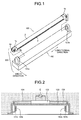
- FIG. 1 is an external perspective view of an illuminating device according to a first embodiment of the present invention;
- FIG. 2 is a cross-section cut along a longitudinal direction of an illuminating lamp member of the illuminating device of the first embodiment;
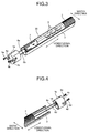
- FIG. 3 is an exploded perspective view of a portion near an end portion on a left side relative to a longitudinal direction of an illuminating lamp of the illuminating device of the first embodiment;
- FIG. 4 is an exploded perspective view of a portion near an end portion on a right side relative to a longitudinal direction of an illuminating lamp of the first embodiment;
- FIG. 5 is an exploded perspective view of a portion near an end portion on a left side relative to the longitudinal direction of the illuminating lamp of the first embodiment;
- FIG. 6 is an exploded perspective view of a portion near an end portion on a right side relative to the longitudinal direction of the illuminating lamp of the first embodiment;
- FIG. 7 is a traversal cross-section of the illuminating lamp of the first embodiment;
- FIG. 8 is a diagram illustrating one example of a functional configuration of the illuminating device of the first embodiment;
- FIG. 9 is an explanatory diagram of one example of a light distribution property of the illuminating lamp;
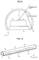
- FIG. 10 is a perspective view of the illuminating lamp of the first embodiment;
- FIG. 11 is a front view of the illuminating lamp of the first embodiment drawn in perspective;
- FIG. 12 is an explanatory diagram of an example of light output control of multiple LEDs in the illuminating lamp of the first embodiment;
- FIG. 13 is an explanatory diagram of one example of a section for verification results of light distribution control of the illuminating lamp of the first embodiment;
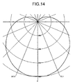
- FIG. 14 is a diagram illustrating a verification result when light distribution is set to be wide;
- FIG. 15 is a diagram illustrating a verification result when light distribution is set to be intermediate;
- FIG. 16 is a diagram illustrating a verification result when light distribution is set to be narrow;
- FIG. 17 is an explanatory diagram of an example of light output control of multiple LEDs in an illuminating lamp of a first modification of the first embodiment;
- FIG. 18 is a diagram illustrating one example of a functional configuration of an illuminating device of a second embodiment of the present invention;
- FIG. 19 is a perspective view of an illuminating lamp of the illuminating device of the second embodiment;
- FIG. 20 is an explanatory diagram of an example of light output control of multiple LEDs in the illuminating lamp of the second embodiment;
- FIG. 21 is an explanatory diagram of one example of a section for verification results of light distribution control of the illuminating lamp of the second embodiment;
- FIG. 22 is a diagram illustrating a verification result when light distribution is set to be wide;
- FIG. 23 is a diagram illustrating a verification result when light distribution is set to be intermediate;
- FIG. 24 is a diagram illustrating a verification result when light distribution is set to be narrow;
- FIG. 25 is a perspective view of an illuminating lamp of a second modification of the second embodiment;
- FIG. 26 is a perspective view of an illuminating lamp of a third modification of the second embodiment; and
- FIG. 27 is a diagram illustrating an image of light beams of the third modification.
DETAILED DESCRIPTION OF THE PREFERRED EMBODIMENTS
-
Embodiments of an illuminating lamp and an illuminating device according to the present invention are explained in detail below with reference to the accompanying drawings.
First Embodiment
-
FIG. 1 is an external perspective view of an illuminating device 200 of the present embodiment. As shown in FIG. 1, the illuminating device 200 includes an illuminating lamp 100, and a lamp member 150 to which the illuminating lamp 100 is attached.
-
The illuminating lamp 100 includes cap members 1a and 1b, a casing 2, and a diffusion cover 3 (one example of a cover member). The casing 2 has a long shape that is formed by extrusion molding a metallic member of, for example, aluminum alloy, magnesium alloy, or the like. Moreover, the casing 2 is formed in a tubular form so as to have a substantially semicircle cross section. The diffusion cover 3 has a long tubular form having a substantially semicircle cross section similarly to the casing 2, so as to form a cylinder having a substantially circular cross section as a whole, in combination with the casing 2. Furthermore, the diffusion cover 3 covers multiple LEDs described later, and is formed with resin or glass so that light beams emitted from the LEDs diffuse therefrom.
-
The cap members 1a and 1b have a bottomed cylindrical shape, and function as a cap at each end of the casing 2 and the diffusion cover 3. Moreover, the cap members 1a and 1b establish physical and electrical connection between the lamp member 150 and the illuminating lamp 100 by being set into sockets 151a and 151b of the lamp member 150. Although the casing 2 is in a substantially semicircle tubular shape in this example, it is not necessarily limited to the substantially semicircle tubular shape. Although the diffusion cover 3 is illustrated in a semicircle in FIG. 1, the diffusion cover 3 may be structured in a cylindrical shape like a fluorescent lamp to wrap the casing 2.
-
FIG. 2 is a cross-section cut along a longitudinal direction of the lamp member 150 of the present embodiment. As shown in FIG. 2, the lamp member 150 includes a fluorescent lamp ballast 153, and the sockets 151a and 151b that detachably connect the illuminating lamp 100, and is configured to be connectable to mains power supply E. The frequency of the mains power supply E is, for example, 50 hertz (Hz), 60 Hz, or the like. The power from the mains power supply E is supplied to the fluorescent lamp ballast 153. As shown in FIG. 2, the lamp member 150 is embedded to, for example, a ceiling or the like on an opposite side to the sockets 151a and 151b, and a side on which the sockets 151a and 151b are arranged is released. The sockets 151a and 151b are connected to the fluorescent lamp ballast 153 through a pair of electrode terminals 152a and 152b and a wiring 154.
-
As the fluorescent lamp ballast 153, for example, a fluorescent-lamp inverter ballast, a fluorescent-lamp glow-starter ballast, and a fluorescent-lamp rapid-starter ballast can be named. However, the illuminating lamp 100 is configured to be connected directly to a mains alternate-current power supply, and in that case, the fluorescent lamp ballast 153 is not necessary. As described, the illuminating lamp 100 can be configured to be connectable to either of the fluorescent-lamp glow-starter ballast, the fluorescent-lamp rapid-starter ballast, the fluorescent-lamp inverter ballast, and the mains alternate-current power supply.
-
FIG. 3 and FIG. 5 are exploded perspective views of a portion near an end portion on a left side relative to a longitudinal direction of the illuminating lamp 100 of the present embodiment. FIG. 4 and FIG. 6 are exploded perspective views of a portion near an end portion on a right side relative to the longitudinal direction of the illuminating lamp 100 of the present embodiment. FIG. 7 is a traversal cross-section of the illuminating lamp 100 of the present embodiment. Note that illustration of a mounting substrate 11a that is arranged on an upper side of a power supply board 7 is omitted in FIG. 3, while the mounting substrate 11a is illustrated in FIG. 5. Similarly, illustration of a mounting substrate 11b is omitted in FIG. 4, while the mounting substrate 11b is illustrated in FIG. 6.
-
As shown in FIG. 3 and FIG. 4, the cap members 1a and 1b are fastened to be fixed to the casing 2 by screws 5a, 5b, 5c, and 5d. Thus, the cap members 1a and 1b covers the casing 2 and the diffusion cover 3 engaged with each other so as to be formed into one piece. That is, the cap members 1a and 1b are formed and arranged so as to cover each end of the casing 2 and the diffusion cover 3.
-
The cap members 1a and 1b may be brought into intimate contact (swaged) with the casing 2 at the joint thereto by a tool and the like, instead of screws, or may be formed by insert molding. The shape of cap members 1a and 1b is approximately the same shape as a cap member (ferrule) positioned at both ends of existing fluorescent lamps. The illuminating lamp 100 can be easily replaced with an existing fluorescent lamp attached to the lamp member 150.
-
As shown in FIG. 3 to FIG. 6, terminals 4a and 4b are arranged at the cap member 1a, and electrode terminals 4c, 4d are arranged at the cap member 1b so as to extrude from the cap member 1a and the cap member 1b, respectively, along the longitudinal direction. When arranging the electrode terminals 4a, 4b, 4c, and 4d to the respective cap members 1a and the cap member 1b, a fixing method, such as insert molding, swaging, and screw fastening, can be used. The illuminating lamp 100 takes alternate current power in from the mains power supply E through connectors 16 and the like that are arranged inside the lamp member 150 and each of the cap members 1a and 1b. The alternate current power taken in is supplied to the power supply board 7 shown in FIG. 3 through lead wires 6a, 6b, 6c, and 6d.
-
On the power supply board 7, an electronic part 9 for a direct-current power conversion to convert the supplied alternate current power into direct current power to supply to the mounting substrates 11a and 11b is arranged. On the mounting substrates 11a and 11b, multiple LEDs 12a are arranged in the longitudinal direction as shown in FIG. 5 and FIG. 6. The LED is one example of a semiconductor light emitting device. In the following, the LEDs 12a may be referred to as an LED load 57 collectively. The power supply board 7 is housed inside the casing in a substantially semicircle tubular shape as shown in FIG. 3, and is fixed not to move inside the casing 2. Moreover, in the case of the illuminating device 200 of the present embodiment, the lead wires 6a and 6b are shorter than the lead wires 6c and 6d.
-
The electric current rectified into a direct current by the electronic part 9 is supplied to the mounting substrates 11a and 11b through lead wires 13a and 13b shown in FIG. 5. The mounting substrates 11a and 11b that are arranged in parallel in the longitudinal direction are electrically connected by a lead wire, a jumper wire, or the like not shown. Although two pieces of the mounting substrates 11a and 11b are illustrated as the mounting substrate to mount the LEDs 12a in this example, in an actual state, another mounting substrate is arranged between the mounting substrates 11a and 11b. One piece, two pieces, or four pieces or more of the mounting substrates may be arranged. In the following, when it is not necessary to distinguish each mounting substrate, it may be referred simply to a mounting substrate 11.
-
As shown in FIGS. 3 to 6, in the case of the illuminating device 200 of the present embodiment, the power supply board 7 is arranged below the mounting substrate 11a, and nothing is arranged on a side of the mounting substrate 11b. In other words, the side of the mounting substrate 11b, it is formed in a flat structure so that the inside of the casing 2 is hollow. Furthermore, on a flat portion 14 that is a portion corresponding to a chord of the semicircle of the casing 2, the mounting substrates 11a and 11b are mounted. Between this flat portion 14 and the mounting substrates 11a and 11b, resin members 10a and 10b in a sheet form are arranged so as to be sandwiched, respectively.
-
The power supply board 7 to which the lead wires 6a and 6b, the lead wires 6c and 6d are connected to the both ends, respectively, as shown in FIG. 3 and FIG. 4, is covered with a holder 30 that is made from resin to be a cover member extending in the longitudinal direction therearound as shown in FIG. 7. At ends of the lead wire 6a and the lead wire 6b, and at ends of the lead wire 6c and the lead wire 6d, ferrule units to insert the respective connectors 16 are arranged. The holder 30 has a long shape having length equivalent to or longer than the power supply board 7, and is a continuous tubular member having no seams in a cross-sectional shape. The holder 30 may be formed by a molding method, such as extrusion molding, pultrusion molding, and injection molding. As a material of the holder 30, for example, polycarbonate (PC) or Polyamide (PA: so-called nylon) is used.
-
The holder 30 can be housed inside the casing 2 as shown in FIG. 7, and has a substantially uniform cross-sectional shape along the longitudinal direction. The power supply board 7 is formed into one piece with the holder 30 by detachably attached to the holder 30.
-
That is, as shown in FIG. 7, on side surfaces 30a and 30b that are positioned in a width direction intersecting the longitudinal direction, pillow portions 31a and 31b are formed, respectively, in an extruding manner in the width direction. These pillow portions 31a and 31b function as guide rail portions when inserting the power supply board 7 into the holder 30 from the end portion. After the power supply board 7 is inserted, the pillow portions 31a and 31b support the power supply board 7 so that a clearance
-
(spaces) 32 is formed between the power supply board 7 and a bottom portion 30c of the holder 30. The clearance 32 is to keep a distance Z1 so that the lead wires of the electronic part 9 shown in FIG. 3, extruding from the power supply board 7 are not in contact with the holder 30, or so that electrical insulation is secured.
-
The holder 30 separates the power supply board 7 from the casing 2 inside the casing 2 by covering the entirety (periphery) of the power supply board 7 from outside. The holder 30 is in contact with an internal surface of the casing 2 inside the casing 2 as shown in FIG. 7. The holder 30 has a smooth surface on a surface being in contact with the internal surface of the casing 2 to be well slidable. In this example, the holder 30 has a cross-sectional shape without seams to split the holder 30. Therefore, when the power supply board 7 is set into the holder 30, the power supply board 7 is to be inserted into the holder 30 from the end portion of the holder 30 that is open. The holder 30 and the power supply board 7 are unified before being set in the casing 2 to form a power-supply board unit, and is then inserted into the casing 2 from the end of the casing 2 in a state being the power supply board unit.
-
According to such a configuration, because the resin holder 30 that covers the periphery of the power supply board 7, that separates the power supply board 7 from the casing 2, and that can be housed inside the casing 2 and extends in the longitudinal direction having a substantially uniform cross-sectional shape is arranged, the electrical insulation with the casing 2 is achieved, and a high level of safety can be ensured. Moreover, coating of an insulating material on the inside of the casing 2 is not necessary to obtain the electric insulation, the casing 2 can be manufactured at low cost. Furthermore, because the power supply board 7 and the casing 2 are separated into sections by the holder 30 inside the casing 2, the lead wires 13a and 13b of the electronic part 9 do not touch the casing 2 even if extruding therefrom, and an expensive part such as a chip part is not necessary to be used for manufacturing.
-
Moreover, in the case of the illuminating device 200 of the present embodiment, because the holder 30 (the bottom portion 30c of the holder 30) is arranged between the power supply board 7 and the mounting substrates 11a and 11b, heat from the power supply board 7 is conducted less to the mounting substrates 11a and 11b, and the influence of heat to the LED load 57 becomes uniform in every LED. Therefore, it is possible to prevent a problem in which life of a part of the LEDs becomes short with time. Furthermore, because a contact surface of the holder 30 that is unified with the power supply board 7 is smoothed, friction resistance can be reduced, and the power-supply board unit can be slid in the casing 2. Therefore, process of inserting the connector 16 to the ferrule unit at each end is facilitated.
-
Moreover, because the holder 30 has no seams in a cross-sectional shape and is formed continuously, the electronic part 9 does not come into direct contact with the casing 2, thereby maintaining the electric insulation with the casing 2, to achieve a high level of safety. Furthermore, because coating on the inside of the casing 2 is not necessary to obtain the electric insulation, the casing 2 can be manufactured at low cost.
-
FIG. 8 is a diagram illustrating one example of a functional configuration of the illuminating device 200 of the present embodiment. AS shown in FIG. 8, the illuminating device 200 includes the mains power supply E, the fluorescent lamp ballast 153, a rectifier unit 310, a control unit 320, and the LED load 57. The rectifier unit 310 and the control unit 320 are arranged on either one of the mounting substrate 11 and the power supply board 7 of the illuminating lamp 100.
-
The rectifier unit 310 is a circuit that performs full-wave rectification on an alternate current signal that is supplied from the mains power supply E through the fluorescent lamp ballast 153, and is, for example, a bridge diode, or the like.
-
The control unit 320 is to control light emission of the LED load 57 (each of the LEDs 12a), and is for example, a driver circuit, or the like. The driver circuit can be implemented by a circuit including a converter, a control integrated circuit (IC), and the like that converts an alternate current signal that has been full-wave rectified by the rectifier unit 310 into a direct current signal. The converter may be of a step-up type or of a step-down type.
-
In the present embodiment, the control unit 320 controls light emission of the LEDs 12a, and controls light distribution of the illuminating lamp 100.
-
The light distribution property of the illuminating lamp 100 is explained. FIG. 9 is an explanatory diagram of one example of the light distribution property of the illuminating lamp 100, and shows a cross-section of the illuminating lamp 100 cut on a Z-Y plane near the end portion on a left side relative to the longitudinal direction.
-
The LED 12a of the present embodiment is a top view LED, and has a property of lambert light distribution, and therefore, emits light in an upward direction (directions mainly of a +Z-axis direction) of the LED 12a. However, because light is only emitted to the upward direction of the LED 12a as it is, the LED 12a is covered with the diffusion cover 3. Thus, light emitted from the LED 12a not only passes through the diffusion cover 3 in the upward direction of the LED 12a, but also light emitted from the LED 12a and reflected on the diffusion cover 3 travels in a horizontal direction (directions mainly of a Y-axis direction) of the LED 12a, and passes through the diffusion cover 3 in the horizontal direction of the LED 12a. Therefore, the illuminating lamp 100 of the present embodiment has the light distribution property of not only the upward direction of the LED 12a but also the horizontal direction of the LED 12a.
-
Light components passing through the diffusion cover 3 in the horizontal direction of the LED 12a increases as a distance L (precisely, the shortest distance) between he LED 12a (precisely, a light source) and the diffusion cover 3 increases, relative to light components passing through the diffusion cover 3 in the upward direction.
-
Therefore, in the present embodiment, the light distribution of the illuminating lamp 100 is controlled by using this property.
-
FIG. 10 and FIG. 11 are explanatory diagrams of an arrangement example of the LEDs 12a of the present embodiment, and FIG. 12 is an explanatory diagram of an example of light output control of the LEDs 12a of the present embodiment. FIG. 10 is a perspective view of the illuminating lamp 100 of the present embodiment, and FIG. 11 is a front view of the illuminating lamp 100 of the present embodiment drawn in perspective.
-
As shown in FIG. 10 and FIG. 11, a distance between the LEDs 12a (an example of at least one first semiconductor-light-emitting device) that are arranged on the mounting substrate 11a and on the mounting substrate 11b and the diffusion cover 3 is L1, and a distance between the LED 12a (an example of at least one second semiconductor-light-emitting device) that is arranged on the mounting substrate 11c and the diffusion cover 3 is L2 (L1<L2).
-
That is, the LED load 57 (multiple LEDs 12a) includes the at least one LED 12a having a first distance from the diffusion cover 3, and the at least one LED 12a having a second distance, that is longer than the first distance, from the diffusion cover 3.
-
The control unit 320 controls light output of the LEDs 12a as shown in FIG. 12 by using a direct current signal obtained by converting an alternate current signal that has been full-wave rectified by the rectifier unit 310, to control the light distribution of the illuminating lamp 100.
-
For example, when setting the light distribution of the illuminating lamp 100 to be wide, the control unit 320 controls the light output of the LEDs 12a arranged on the mounting substrate 11c to 100%, and the light output of the LEDs 12a arranged on the mounting substrate 11a and the mounting substrate 11b to 0%.
-
Moreover, for example, when setting the light distribution of the illuminating lamp 100 to be intermediate (normal), the control unit 320 controls the light output of the LEDs 12a arranged on the mounting substrate 11c to 50%, and the light output of the LEDs 12a arranged on the mounting substrate 11a and the mounting substrate 11b to 25%.
-
Furthermore, for example, when setting the light distribution of the illuminating lamp 100 to be narrow, the control unit 320 controls the light output of the LEDs 12a arranged on the mounting substrate 11c to 0%, and the light output of the LEDs 12a arranged on the mounting substrate 11a and the mounting substrate 11b to 100%.
-
Note that the maximum light amount in each of the mounting substrates is identical in any of the light distribution settings in the example shown in FIG. 12.
-
That is, when setting to widen the light distribution of the illuminating lamp 100, the control unit 320 controls the light output of the LED 12a (the LED 12a having the distance from the diffusion cover 3 of L2) arranged on the mounting substrate 11c to be larger than the light output of the LEDs 12a (the LEDs 12a having the distance from the diffusion cover 3 of L1) arranged on the mounting substrate 11a and the mounting substrate 11b.
-
Furthermore, when setting to narrow the light distribution of the illuminating lamp 100, the control unit 320 controls the light output of the LEDs 12a (the LEDs 12a having the distance from the diffusion cover 3 of L1) arranged on the mounting substrate 11a and the mounting substrate 11b to be larger than the light output of the LED 12a (the LED 12a having the distance from the diffusion cover 3 of L2) arranged on the mounting substrate 11c.
-
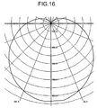
FIG. 13 to FIG. 16 are explanatory diagrams of a result of verification of the light distribution control shown in FIG. 12 by optical simulation, and FIG. 14 illustrates a verification result when the light distribution is set to be wide, FIG. 15 illustrates a verification result when the light distribution is set to be intermediate, and FIG. 16 illustrates a verification result when the light distribution is set to be narrow. Either of the verification results shown in FIG. 14 to FIG. 16 indicates a verification result on a Z-Y plane of the illuminating lamp 100 shown in FIG. 13.
-
In the example shown in FIG. 14, a spread angle of a beam is approximately 160 degrees, in the example shown in FIG. 15, a spread angle of a beam is approximately 145 degrees, and in the example shown in FIG. 16, a spread angle of a beam is approximately 130 degrees, and it is observed that as the light output of the LED 12a arranged on the mounting substrate 11c becomes larger relative to the light output of the LEDs 12a arranged on the mounting substrate 11a and the mounting substrate 11b, the light distribution becomes wider, and that as the light output of the LEDs 12a arranged on the mounting substrate 11a and the mounting substrate 11b becomes larger relative to the light output of the LED 12a arranged on the mounting substrate 11c, the light distribution becomes narrower. The spread angle of a beam indicates a magnitude of angle of light at the intensity of ±1/2 relative to the maximum intensity.
-
As described, according to the first embodiment, the light distribution is controlled without using a lens, and therefore, the light distribution can be controlled without deteriorating the optical efficiency, while suppressing cost increase.
First Modification
-
The first embodiment may be combined with a toning function. For example, setting the light color of the LED 12a arranged on the mounting substrate 11c to a warm white color, and the light color of the LEDs 12a arranged on the mounting substrate 11a and the mounting substrate 11b to a neutral (daylight) color, the control unit 320 may be configured to control the light distribution and the toning of the illuminating lamp 100 by controlling the light output of the LEDs 12a as shown in FIG. 17.
-
For example, in a case of a relaxing mode setting, the control unit 320 controls the light output of the LED 12a arranged on the mounting substrate 11c to 100%, the light output of the LEDs 12a arranged on the mounting substrate 11a and the mounting substrate 11b to 0%, and therefore, the light distribution can be set to be wide and the light color can be made calm color like a warm white color, thereby making a space producing a relaxing effect.
-
Furthermore, for example, in a case of a centralized mode setting, the control unit 320 controls the light output of the LED 12a arranged on the mounting substrate 11c to 0%, the light output of the LEDs 12a arranged on the mounting substrate 11a and the mounting substrate 11b to 100%, and therefore, the light distribution can be set to be narrow and the light color can be made daylight color, thereby making a space producing a work efficiency improvement effect.
Second Embodiment
-
In a second embodiment, a light distribution control example different from that of the first embodiment is explained. In the following, a difference from the first embodiment is mainly explained, and as for components having similar functions as the first embodiment, the same names and symbols as the first embodiment are given, and explanation thereof is omitted.
-
FIG. 18 is a diagram illustrating one example of a functional configuration of the illuminating device 200 of the present embodiment, and a control unit 420 is different from the first embodiment.
-
FIG. 19 is an explanatory diagram of an arrangement example of LEDs 512a and 512b of the present embodiment, and FIG. 20 is an explanatory diagram of an example of light output control of the LEDs 512a and 512b of the present embodiment. FIG. 19 is a perspective view of the illuminating lamp 100 of the present embodiment.
-
In the example shown in FIG. 19, a mounting substrate 511 is mounted in a single piece, and the LED 512a (an example of the first semiconductor-light-emitting device) and the LED 512b (an example of the second semiconductor-light-emitting device) are alternately arranged in the longitudinal direction. The LED 512a is a top view LED, and the LED 512b is a chip through LED. Unlike the top view LED, because the chip through LED has no reflector, light is emitted not only upward but also horizontally, and therefore, the light distribution thereof is wider than that of the top view LED.
-
That is, the LED load 57 (the multiple units of the LEDs 512a and LEDs 512b) includes the at least one LED 512a and the at least one LED 512b having wider light distribution than that of the LED 512a.
-
The control unit 420 controls the light output of the LEDs 512a and 512b as shown in FIG. 20 by using a direct current signal that is obtained by converting an alternate current signal that has been full-wave rectified by the rectifier unit 310, to control the light distribution of the illuminating lamp 100.
-
For example, when setting the light distribution of the illuminating lamp 100 to be wide, the control unit 420 controls the light output of the LEDs 512b to 100%, and the light output of the LEDs 512a to 0%.
-
Moreover, for example, when setting the light distribution of the illuminating lamp 100 to be intermediate (normal), the control unit 420 controls the light output of the LEDs 512b to 50%, and the light output of the LEDs 512a to 25%.
-
Furthermore, for example, when setting the light distribution of the illuminating lamp 100 to be narrow, the control unit 420 controls the light output of the LEDs 512b to 0%, and the light output of the LEDs 512a to 100%.
-
Note that the maximum light amount in each LED is identical in any of the light distribution settings in the example shown in FIG. 20.
-
That is, when setting to widen the light distribution of the illuminating lamp 100, the control unit 420 controls the at least one light output of the LED 512b to be larger than the light output of the at least one LEDs 512a.
-
Furthermore, when setting to narrow the light distribution of the illuminating lamp 100, the control unit 420 controls the light output of the at least one LED 512a to be larger than the light output of the at least one LED 512b.
-
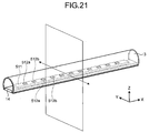
FIG. 21 to FIG. 24 are explanatory diagrams of a result of verification of the light distribution control shown in FIG. 20 by optical simulation, and FIG. 22 illustrates a verification result when the light distribution is set to be wide, FIG. 23 illustrates a verification result when the light distribution is set to be intermediate, and FIG. 24 illustrates a verification result when the light distribution is set to be narrow. Either of the verification results shown in FIG. 22 to FIG. 24 indicates a verification result on a Z-Y plane of the illuminating lamp 100 shown in FIG. 21.
-
In the example shown in FIG. 22, a spread angle of a beam is approximately 200 degrees, and in the example shown in FIG. 23, a spread angle of a beam is approximately 175 degrees, an in the example shown in FIG. 24, a spread angle of a bema is approximately 150 degrees, and it is observed that as the light output of the LED 512b becomes larger relative to the light output of the LEDs 512a, the light distribution becomes wider, and that as the light output of the LEDs 512a becomes larger relative to the light output of the LED 512b, the light distribution becomes narrower.
-
As described, according to the second embodiment also, the light distribution is controlled without using a lens, and therefore, the light distribution can be controlled without deteriorating the optical efficiency, while suppressing cost increase.
Second Modification
-
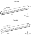
In the second embodiment, as shown in FIG. 25, instead of the LEDs 512b, chip-on-board LEDs 512c may be used. The chip-on-board LED 512c also emits light not only upward, but also horizontally, and therefore, the light distribution thereof is wider than that of the top view LED.
-
In the second modification also, the light distribution is controlled without using a lens, and therefore, the light distribution can be controlled without deteriorating the optical efficiency, while suppressing cost increase.
Third Modification
-
In the second embodiment, as shown in FIG. 26, instead of the LEDs 512b, side view LEDs 512d may be used. The side view LED 512d emits light horizontally. In the example shown in FIG. 26, a light beam image is as shown in FIG. 27.
-
In the third modification also, the light distribution is controlled without using a lens, and therefore, the light distribution can be controlled without deteriorating the optical efficiency, while suppressing cost increase.
-
According to the embodiments of the present invention, an effect that light distribution can be controlled without deteriorating optical efficiency, while suppressing cost increase.
-
Although the invention has been described with respect to specific embodiments for a complete and clear disclosure, the appended claims are not to be thus limited but are to be construed as embodying all modifications and alternative constructions that may occur to one skilled in the art that fairly fall within the basic teaching herein set forth.