EP3010105A1 - Systems and methods for capacitor charge extraction - Google Patents
Systems and methods for capacitor charge extraction Download PDFInfo
- Publication number
- EP3010105A1 EP3010105A1 EP15189544.8A EP15189544A EP3010105A1 EP 3010105 A1 EP3010105 A1 EP 3010105A1 EP 15189544 A EP15189544 A EP 15189544A EP 3010105 A1 EP3010105 A1 EP 3010105A1
- Authority
- EP
- European Patent Office
- Prior art keywords
- boost converter
- capacitor
- state
- voltage
- power
- Prior art date
- Legal status (The legal status is an assumption and is not a legal conclusion. Google has not performed a legal analysis and makes no representation as to the accuracy of the status listed.)
- Granted
Links
Images


Classifications
-
- H—ELECTRICITY
- H02—GENERATION; CONVERSION OR DISTRIBUTION OF ELECTRIC POWER
- H02J—ELECTRIC POWER NETWORKS; CIRCUIT ARRANGEMENTS OR SYSTEMS FOR SUPPLYING OR DISTRIBUTING ELECTRIC POWER; SYSTEMS FOR STORING ELECTRIC ENERGY
- H02J1/00—Circuit arrangements for DC mains or DC distribution networks
- H02J1/10—Parallel operation of DC sources
- H02J1/12—Parallel operation of DC sources having power converters with further DC sources without power converters
-
- H—ELECTRICITY
- H02—GENERATION; CONVERSION OR DISTRIBUTION OF ELECTRIC POWER
- H02M—APPARATUS FOR CONVERSION BETWEEN AC AND AC, BETWEEN AC AND DC, OR BETWEEN DC AND DC, AND FOR USE WITH MAINS OR SIMILAR POWER SUPPLY SYSTEMS; CONVERSION OF DC OR AC INPUT POWER INTO SURGE OUTPUT POWER; CONTROL OR REGULATION THEREOF
- H02M3/00—Conversion of DC power input into DC power output
- H02M3/02—Conversion of DC power input into DC power output without intermediate conversion into AC
- H02M3/04—Conversion of DC power input into DC power output without intermediate conversion into AC by static converters
-
- H—ELECTRICITY
- H02—GENERATION; CONVERSION OR DISTRIBUTION OF ELECTRIC POWER
- H02J—ELECTRIC POWER NETWORKS; CIRCUIT ARRANGEMENTS OR SYSTEMS FOR SUPPLYING OR DISTRIBUTING ELECTRIC POWER; SYSTEMS FOR STORING ELECTRIC ENERGY
- H02J50/00—Circuit arrangements or systems for wireless supply or distribution of electric power
- H02J50/001—Energy harvesting or scavenging
-
- H—ELECTRICITY
- H02—GENERATION; CONVERSION OR DISTRIBUTION OF ELECTRIC POWER
- H02J—ELECTRIC POWER NETWORKS; CIRCUIT ARRANGEMENTS OR SYSTEMS FOR SUPPLYING OR DISTRIBUTING ELECTRIC POWER; SYSTEMS FOR STORING ELECTRIC ENERGY
- H02J7/00—Circuit arrangements for charging or discharging batteries or for supplying loads from batteries
- H02J7/34—Parallel operation in networks using both storage and other DC sources, e.g. providing buffering
- H02J7/345—Parallel operation in networks using both storage and other DC sources, e.g. providing buffering using capacitors as storage or buffering devices
-
- H—ELECTRICITY
- H02—GENERATION; CONVERSION OR DISTRIBUTION OF ELECTRIC POWER
- H02J—ELECTRIC POWER NETWORKS; CIRCUIT ARRANGEMENTS OR SYSTEMS FOR SUPPLYING OR DISTRIBUTING ELECTRIC POWER; SYSTEMS FOR STORING ELECTRIC ENERGY
- H02J7/00—Circuit arrangements for charging or discharging batteries or for supplying loads from batteries
- H02J7/865—Battery or charger load switching, e.g. concurrent charging and load supply
-
- H—ELECTRICITY
- H02—GENERATION; CONVERSION OR DISTRIBUTION OF ELECTRIC POWER
- H02M—APPARATUS FOR CONVERSION BETWEEN AC AND AC, BETWEEN AC AND DC, OR BETWEEN DC AND DC, AND FOR USE WITH MAINS OR SIMILAR POWER SUPPLY SYSTEMS; CONVERSION OF DC OR AC INPUT POWER INTO SURGE OUTPUT POWER; CONTROL OR REGULATION THEREOF
- H02M3/00—Conversion of DC power input into DC power output
- H02M3/02—Conversion of DC power input into DC power output without intermediate conversion into AC
- H02M3/04—Conversion of DC power input into DC power output without intermediate conversion into AC by static converters
- H02M3/10—Conversion of DC power input into DC power output without intermediate conversion into AC by static converters using discharge tubes with control electrode or semiconductor devices with control electrode
- H02M3/145—Conversion of DC power input into DC power output without intermediate conversion into AC by static converters using discharge tubes with control electrode or semiconductor devices with control electrode using devices of a triode or transistor type requiring continuous application of a control signal
- H02M3/155—Conversion of DC power input into DC power output without intermediate conversion into AC by static converters using discharge tubes with control electrode or semiconductor devices with control electrode using devices of a triode or transistor type requiring continuous application of a control signal using semiconductor devices only
Definitions
- a system for providing electrical power to a load includes a boost converter with an input and an output.
- the boost converter is configured to receive power at a first voltage at the input, and to supply power at a higher second voltage from the output.
- a capacitor e.g., a super capacitor, is operatively connected between the output of the boost converter and a ground node.
- a first switch is operatively connected between the first input node and the output of the boost converter for switching between a first state connecting the capacitor to the output of the boost converter and a second state connecting the capacitor to supply input voltage to the input of the boost converter.
- the method can include switching from the second state to the first state when sufficient power becomes available from the power source. It is also contemplated that the method can include sensing voltages of the power source and capacitor, wherein switching from the first state to the second state and switching from the second state to the first state includes switching based on the voltages sensed. It is further contemplated that switching from the second state to the first state can include connecting the capacitor to a charge network before connecting the capacitor to the output of the boost converter in the event that the capacitor voltage is below a predetermined threshold at the time of switching to the first state in order to avoid starving the load when connecting the capacitor to the output of the boost converter.
- FIG. 2 a partial view of an exemplary embodiment of a system in accordance with the disclosure is shown in Fig. 2 and is designated generally by reference character 100.
- FIGs. 3-5 Other embodiments of systems in accordance with the disclosure, or aspects thereof, are provided in Figs. 3-5 , as will be described.
- the systems and methods described herein can be used to provide power to loads with improved capacitor utilization.
- system 10 of Fig. 1 e.g., a traditional energy harvesting circuit, does a good job of extracting the low voltage energy of the source, and provides a backup source of energy with the super capacitor 18, a typical low power electrical load will not effectively use all the energy stored during the super capacitor charge phase.
- a typical 3.3V load circuit many analog integrated circuits will cease to function at about 2.3V and numerous high performance microcontrollers lose I/O functionality at 3.15V.
Landscapes
- Engineering & Computer Science (AREA)
- Power Engineering (AREA)
- Computer Networks & Wireless Communication (AREA)
- Charge And Discharge Circuits For Batteries Or The Like (AREA)
- Dc-Dc Converters (AREA)
Abstract
Description
- The present disclosure relates to power supply systems, and more particularly to extracting charges from super capacitors as in energy harvesting applications.
- Typical energy harvesting systems include a low voltage energy harvester, such as an inertial generator, thermoelectric generator, or solar panel, a boost converter for raising the low voltage from the energy harvester to a nominal level for a specific load, and an energy storage device such as a battery, super capacitor, or the like. The harvester supplies low voltage power to the boost converter, which raises the voltage to within an acceptable input voltage range for the load. When using a super capacitor, for example, a first plate of the super capacitor is connected between the boost converter and load, and the second plate is connected to ground. In this position, the super capacitor can accumulate energy when the output voltage of the boost converter is high, and can discharge energy to the load when the boost converter output voltage drops off, as when the harvester is not producing energy. This system helps maintain the input voltage to the load within an acceptable range despite the fact that the energy production of the harvester may be highly variable over time.
- Such conventional methods and systems have generally been considered satisfactory for their intended purpose. However, there is still a need in the art for improved management of power from energy harvesters and the like. The present disclosure provides a solution for this need.
- A system for providing electrical power to a load includes a boost converter with an input and an output. The boost converter is configured to receive power at a first voltage at the input, and to supply power at a higher second voltage from the output. A capacitor, e.g., a super capacitor, is operatively connected between the output of the boost converter and a ground node. A first switch is operatively connected between the first input node and the output of the boost converter for switching between a first state connecting the capacitor to the output of the boost converter and a second state connecting the capacitor to supply input voltage to the input of the boost converter.
- A charge decision controller can be operatively connected to a first input node to detect voltage of the capacitor. The charge decision controller can be operatively connected to detect voltage at a second input node selectively connected to the input of the boost converter. A second switch can be operatively connected between the second input node and the input of the boost converter for switching between a first state connecting the boost converter to the second input node to receive power from a power source, and a second state disconnecting the boost converter from the second input node. The charge decision controller is configured to command the first and second switches into their respective second states upon detection of voltage below a first predetermined limit at the second input node and voltage of the capacitor below a second predetermined limit.
- The charge decision controller can be configured to command the first and second switches into their respective first states upon detection of voltage above the first predetermined limit at the second input node and/or voltage of the capacitor above the second predetermined limit. The system can include a charge network operatively connected between the output of the boost converter and the first switch, wherein the first switch includes a third state for connecting the capacitor to a charge network to avoid allowing the capacitor to draw power needed for a load connected to the output of the boost converter when charging the capacitor. The first and second switches can be electrically connected to one another to provide an electrical connection from the capacitor to power the boost converter in the second state of the first and second switches. A power source can be operatively connected to the second input node, e.g., wherein the power source includes an energy harvester.
- A method of supplying power includes supplying power to a load in a first state of a power supply system. The first state includes powering a load from a power source connected to an input of a boost converter, wherein the output of the boost converter is connected to the load to raise the voltage from the power source to above a minimum acceptable level for the load; charging a capacitor, e.g., a super capacitor, connected between the output of the boost converter and a ground node when the output voltage of the boost converter is higher than the voltage of the capacitor; and powering the load from the capacitor when the voltage of the capacitor is higher than the output voltage of the boost converter. The method also includes switching to a second state of the power supply system to supply power to the load when power from the power source is insufficient and the voltage of the capacitor is below the minimum acceptable level for the load, wherein switching to the second state includes: disconnecting the power source from the boost converter; and connecting the capacitor to the input of the boost capacitor to supply power to the load from the capacitor.
- The method can include switching from the second state to the first state when sufficient power becomes available from the power source. It is also contemplated that the method can include sensing voltages of the power source and capacitor, wherein switching from the first state to the second state and switching from the second state to the first state includes switching based on the voltages sensed. It is further contemplated that switching from the second state to the first state can include connecting the capacitor to a charge network before connecting the capacitor to the output of the boost converter in the event that the capacitor voltage is below a predetermined threshold at the time of switching to the first state in order to avoid starving the load when connecting the capacitor to the output of the boost converter.
- These and other features of the systems and methods of the subject disclosure will become more readily apparent to those skilled in the art from the following detailed description of the preferred embodiments taken in conjunction with the drawings.
- So that those skilled in the art to which the subject disclosure appertains will readily understand how to make and use the devices and methods of the subject disclosure without undue experimentation, preferred embodiments thereof will be described by way of example only and in detail herein below with reference to certain figures, wherein:
-
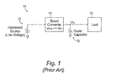
Fig. 1 is a schematic view of a prior art system for providing electrical power, showing a harvested source, boost converter, and super capacitor; -
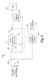
Fig. 2 is a schematic view of an exemplary embodiment of a system for providing electrical power constructed in accordance with the present disclosure, showing the system in a first state supplying power from a harvested source through a boost converter, charging or drawing from the super capacitor as needed; -
Fig. 3 is a schematic view of the system ofFig. 2 , showing a second state wherein the super capacitor powers the boost converter to supply power to the load; -
Fig. 4 is a schematic view of the system ofFig. 2 , showing a third sate wherein the super capacitor connects through a charge network to avoid starving the load before returning to the first state shown inFig. 2 ; and -
Fig. 5 is a block diagram showing different conditions of the systems based on voltage of the super capacitor and harvested source. - Reference will now be made to the drawings wherein like reference numerals identify similar structural features or aspects of the subject disclosure. For purposes of explanation and illustration, and not limitation, a partial view of an exemplary embodiment of a system in accordance with the disclosure is shown in
Fig. 2 and is designated generally byreference character 100. Other embodiments of systems in accordance with the disclosure, or aspects thereof, are provided inFigs. 3-5 , as will be described. The systems and methods described herein can be used to provide power to loads with improved capacitor utilization. - Referring first to
Fig. 1 , a typicalenergy harvesting system 10 includes a lowvoltage energy harvester 12, such as an inertial generator or solar panel, aboost converter 14 for raising the low voltage from theenergy harvester 12 to a nominal level for aspecific load 16, and an energy storage device such as a battery,super capacitor 18, or the like. Theharvester 12 supplies low voltage power to theboost converter 14, which raises the voltage to within an acceptable input voltage range for theload 16. When using a super capacitor, for example, a first plate of thesuper capacitor 18 is connected between the boost converter andload 16, and the second plate is connected to ground. In this position, thesuper capacitor 18 can accumulate energy when the output voltage of theboost converter 14 is high, and can discharge energy to theload 16 when the boost converter 14 output voltage drops off, as when theharvester 12 is not producing energy. This system helps maintain the input voltage to theload 16 within an acceptable range despite the fact that the energy production of theharvester 12 may be highly variable over time. - While
system 10 ofFig. 1 , e.g., a traditional energy harvesting circuit, does a good job of extracting the low voltage energy of the source, and provides a backup source of energy with thesuper capacitor 18, a typical low power electrical load will not effectively use all the energy stored during the super capacitor charge phase. For example, with a typical 3.3V load circuit, many analog integrated circuits will cease to function at about 2.3V and numerous high performance microcontrollers lose I/O functionality at 3.15V. With a fixed capacitance value of thesuper capacitor 18, this is the equivalent of only using about 51% and 9%, respectively, of the total stored energy. If the super capacitor can be discharged down to 0.2V, for example using the systems and methods disclosed herein, the lower input range of typical energy harvesting boost converters, nearly 100% of the stored energy in a super capacitor can be utilized. - With reference now to
Fig. 2 , asystem 100 for providing electrical power to aload 116 in accordance with the present disclosure includes aboost converter 114 with aninput 120 and anoutput 122. Theboost converter 114 is configured to receive power at a first voltage at the input, and to supply power at a higher second voltage from the output. Acapacitor 118, e.g., a super capacitor, is operatively connected between theoutput 122 of theboost converter 114 and a ground node. Acharge decision controller 124 is operatively connected to afirst input node 126 to detect voltage of thecapacitor 118 and is operatively connected to detect voltage at asecond input node 128 selectively connected to theinput 120 of theboost converter 114. Afirst switch 130 is operatively connected between thefirst input node 126 and theoutput 122 of theboost converter 114 for switching between a first state, shown inFig. 2 , connecting thecapacitor 118 to theoutput 122 of the boost converter and a second state, shown inFig. 3 connecting thecapacitor 118 to supply input voltage to theinput 120 of theboost converter 114. - A
second switch 132 is operatively connected between thesecond input node 128 and theinput 120 of theboost converter 114 for switching between a first state, shown inFig. 2 , connecting theboost converter 114 to thesecond input node 128 to receive power from a power source, e.g., a harvestedpower source 112, and a second state, shown inFig. 3 , disconnecting theboost converter 114 from thesecond input node 128. Thecharge decision controller 124 is configured to command the first andsecond switches second input node 128 and voltage of thecapacitor 118, i.e., at thefirst input node 126 below a second predetermined limit L. Thecharge decision controller 124 is configured to command the first andsecond switches second input node 128 and/or voltage of thecapacitor 118 above the second predetermined limit L. -
System 100 includes acharge network 134 operatively connected between theoutput 122 of theboost converter 114 and thefirst switch 130. Thefirst switch 130 includes a third state, as shown inFig. 4 , for connecting thecapacitor 118 to chargenetwork 134 configured to avoid allowing thecapacitor 118 to draw power needed for theload 116 connected to theoutput 122 of theboost converter 114 when charging thecapacitor 118. For example, if the charge oncapacitor 118 is low enough to starveload 116 if they are both connected directly tooutput 122,charge network 134 will allowcapacitor 118 to charge without starvingload 116. The first andsecond switches line 136, to provide an electrical connection from thecapacitor 118 to power theboost converter 114 in the second state of the first andsecond switches - With reference now to
Fig. 5 , a method of supplying power is described. The method includes supplying power to a load,e.g. load 116, in a first state of a power supply system, e.g.,system 100. The first state includes powering the load from a power source, e.g.,power source 112, connected to an input of a boost converter, e.g.,boost converter 114, wherein the output of the boost converter is connected to the load to raise the voltage from the power source to above a minimum acceptable level for the load; charging a capacitor, e.g.,capacitor 118, connected between the output of the boost converter and a ground node when the output voltage of the boost converter is higher than the voltage of the capacitor; and powering the load from the capacitor when the voltage of the capacitor is higher than the output voltage of the boost converter. The method also includes switching to a second state, indicated bybox 204 inFig. 5 , of the power supply system to supply power to the load when power from the power source is insufficient, e.g., below the first predetermined limit K, and the voltage of the capacitor is below the minimum acceptable level for the load, e.g., the capacitor voltage is below the second predetermined limit L. Switching to the second state includes: disconnecting the power source from the boost converter; and connecting the capacitor to the input of the boost capacitor to supply power to the load from the capacitor. - The method can include switching from the second state,
e.g. box 204, to the first state when sufficient power becomes available from the power source. It is also contemplated that the method can include sensing voltages of the power source and capacitor, wherein switching from the first state to the second state and switching from the second state to the first state includes switching based on the voltages sensed. It is further contemplated that switching from the second state to the first state can include connecting the capacitor to a charge network, e.g.,charge network 134, before connecting the capacitor to the output of the boost converter in the event that the capacitor voltage is below a predetermined threshold L, as indicated bybox 208 inFig. 5 , at the time of switching to the first state in order to avoid starving the load when connecting the capacitor to the output of the boost converter. Once the charge decision circuit determines that the capacitor will not overload the boost converter, it returns the system to the first state, e.g., as shown inFig. 2 .Boxes Fig. 5 denote normal operation instate 1, wherein the load is powered by the capacitor and by the power source, respectively.Box 210 inFig. 5 represents a state where there is insufficient power from the power source, e.g.,power source 112, and from the capacitor to power the load. To avoid ever reaching this state, design choices can be made to provide sufficient power to a given load by ensuring enough power is available at all times from the power source and capacitor. - The systems and methods described herein provide enhanced utilization of energy stored in the capacitor compared to traditional systems. The difference between the first predetermined voltage K and the second predetermined voltage L represents voltage in the capacitor that traditional systems would not be able to utilize, but which systems and methods disclosed herein can utilize. While described herein in the exemplary context of capacitors and super capacitors, those skilled in the art will readily appreciate that any suitable power storage device can be used. For example, batteries can be used in addition to or in lieu of capacitors or super capacitors as described herein. A practical limitation is that many existing battery chemistries will exhibit reduced lifetimes if they are often discharged to nearly zero volts. While described herein in the exemplary context of energy harvesters, those skilled in the art will readily appreciate that any other suitable power source can be used.
- The methods and systems of the present disclosure, as described above and shown in the drawings, provide for systems and methods of providing power, e.g., from harvested sources, with superior properties including improved capacitor utilization. While the apparatus and methods of the subject disclosure have been shown and described with reference to preferred embodiments, those skilled in the art will readily appreciate that changes and/or modifications may be made thereto without departing from the scope of the subject disclosure.
Claims (14)
- A system (100) for providing electrical power to a load comprising:a boost converter (114) with an input (120) and an output (122);an energy storage device (118) operatively connected between the output (122) of the boost converter (114) and a ground node; anda first switch (130) operatively connected between a first input node (126) and the output (122) of the boost converter (114), the switch having a first state connecting the energy storage device (118) to the output (122) of the boost converter (114) and a second state connecting the energy storage device (118) to supply input voltage to the input (120) of the boost converter (114).
- A system (100) as recited in claim 1, wherein the energy storage device (118) is a super capacitor.
- A system (100) as recited in claim 2, further comprising a charge decision controller (124) operatively connected to the first input node (126) to detect voltage of the energy storage device (118), wherein the charge decision controller (124) is operatively connected to detect voltage at a second input node (128) selectively connected to the input (120) of the boost converter (114).
- A system (100) as recited in claim 3, further comprising a second switch (132) operatively connected between the second input node (128) and the input (120) of the boost converter (114), the second switch (132) having a first state connecting the boost converter (114) to the second input node (128) to receive power from a power source, and a second state disconnecting the boost converter (114) from the second input node (128), wherein the charge decision controller (124) is operatively connected to command the first and second switches (130, 132) into their respective second states upon detection of voltage below a first predetermined limit at the input node (126) and voltage of the capacitor below a second predetermined limit.
- A system (100) as recited in claim 4, wherein the charge decision controller (124) is operatively connected to command the first and second switches (130, 132) into their respective first states upon detection of voltage above the first predetermined limit at the input node (126) and/or voltage of the capacitor above the second predetermined limit.
- A system (100) as recited in claim 4, further comprising a charge network (134) operatively connected between the output (122) of the boost converter (114) and the first switch, wherein the first switch (130) includes a third state connecting the capacitor (118) to the charge network (134) to avoid allowing the capacitor to draw power needed for a load connected to the output (122) of the boost converter (114) when charging the capacitor.
- A system (100) as recited in claim 4, wherein the first and second switches (130, 132) are electrically connected to one another to provide an electrical connection from the capacitor to power the boost converter (114) in the second state of the first and second switches (130, 132).
- A system (100) as recited in claim 4, further comprising a power source operatively connected to the second input node (128).
- A system as recited in claim 8, wherein the power source includes an energy harvester.
- A method of supplying power comprising:supplying power to a load in a first state of a power supply system, wherein the first state includes:powering a load from a power source connected to an input (120) of a boost converter (114), wherein an output (122) of the boost converter (114) is connected to the load to raise the voltage from the power source to above a minimum acceptable level for the load;charging an energy storage device (118) connected between the output (122) of the boost converter (124) and a ground node when the output voltage of the boost converter (114) is higher than the voltage of the storage device (118); andpowering the load from the storage device (118) when the voltage of the storage device (118) is higher than the output voltage of the boost converter (114); andswitching to a second state of the power supply system to supply power to the load when power from the power source is insufficient and the voltage of the storage device is below the minimum acceptable level for the load, wherein switching to the second state includes:disconnecting the power source from the boost converter (114); andconnecting the storage device (118) to the input (120) of the boost converter (114) to supply power to the load from the storage device (118).
- A method as recited in claim 10, wherein the storage device (118) is a super capacitor.
- A method as recited in claim 11, further comprising switching from the second state to the first state when sufficient power becomes available from the power source.
- A method as recited in claim 12, further comprising sensing voltages of the power source and capacitor, wherein switching from the first state to the second state and switching from the second state to the first state includes switching based on the voltages sensed.
- A method as recited in claim 11, wherein switching from the second state to the first state includes connecting the capacitor (118) to a charge network (134) before connecting the capacitor to the output (122) of the boost converter (114) in the event that the capacitor voltage is below a predetermined threshold at the time of switching to the first state in order to avoid starving the load when connecting the capacitor (118) to the output (122) of the boost converter (114).
Applications Claiming Priority (1)
| Application Number | Priority Date | Filing Date | Title |
|---|---|---|---|
| US14/514,174 US9590497B2 (en) | 2014-10-14 | 2014-10-14 | Systems and methods for capacitor charge extraction |
Publications (2)
| Publication Number | Publication Date |
|---|---|
| EP3010105A1 true EP3010105A1 (en) | 2016-04-20 |
| EP3010105B1 EP3010105B1 (en) | 2019-06-19 |
Family
ID=54325396
Family Applications (1)
| Application Number | Title | Priority Date | Filing Date |
|---|---|---|---|
| EP15189544.8A Not-in-force EP3010105B1 (en) | 2014-10-14 | 2015-10-13 | Systems and methods for capacitor charge extraction |
Country Status (4)
| Country | Link |
|---|---|
| US (1) | US9590497B2 (en) |
| EP (1) | EP3010105B1 (en) |
| BR (1) | BR102015026102A2 (en) |
| CA (1) | CA2909014A1 (en) |
Cited By (2)
| Publication number | Priority date | Publication date | Assignee | Title |
|---|---|---|---|---|
| CN110023872A (en) * | 2016-09-15 | 2019-07-16 | 雷神公司 | Charging management system |
| CN111157780A (en) * | 2019-12-28 | 2020-05-15 | 杭州拓深科技有限公司 | Power failure alarm device and control method thereof |
Families Citing this family (13)
| Publication number | Priority date | Publication date | Assignee | Title |
|---|---|---|---|---|
| US10903678B2 (en) * | 2014-10-21 | 2021-01-26 | Maxwell Technologies, Inc. | Apparatus and method for providing bidirectional voltage support |
| US9800143B2 (en) | 2016-03-03 | 2017-10-24 | The Regents Of The University Of Michigan | Moving-sum charge pump |
| US10476382B2 (en) * | 2016-03-03 | 2019-11-12 | The Regents Of The University Of Michigan | Energy harvester |
| JP6772784B2 (en) * | 2016-11-25 | 2020-10-21 | 富士通株式会社 | Power control circuit, energy harvesting device and control method of energy harvesting device |
| WO2019179752A1 (en) * | 2018-03-23 | 2019-09-26 | E-Peas S.A. | Method and device for charging a storage device with energy from an energy harvester |
| JP6732837B2 (en) * | 2018-04-27 | 2020-07-29 | 矢崎総業株式会社 | Power redundancy system |
| EP3736177B1 (en) * | 2019-05-08 | 2022-02-23 | Ningbo Geely Automobile Research & Development Co., Ltd. | A method for controlling a super capacitor module for a vehicle with a high voltage power source |
| CN116326207B (en) * | 2020-10-08 | 2026-04-10 | 昕诺飞控股有限公司 | Drivers for loads and corresponding LED-based lighting devices and methods. |
| JP7588542B2 (en) * | 2021-04-06 | 2024-11-22 | エイブリック株式会社 | Simulation device, simulation method, simulation system and program |
| US12015341B2 (en) * | 2021-04-12 | 2024-06-18 | Wiliot, LTD. | Oscillator voltage reference method and apparatus |
| CN114884203A (en) * | 2022-06-08 | 2022-08-09 | 超聚变数字技术有限公司 | Power supply device and method |
| US12580412B2 (en) * | 2023-08-01 | 2026-03-17 | Schneider Electric It Corporation | High efficiency line VFI UPS invention |
| US20250112550A1 (en) * | 2023-09-29 | 2025-04-03 | Apple Inc. | Tank capacitor charging for pulsed load applications |
Citations (2)
| Publication number | Priority date | Publication date | Assignee | Title |
|---|---|---|---|---|
| KR20110073635A (en) * | 2009-12-24 | 2011-06-30 | 두산인프라코어 주식회사 | Power converter of hybrid industrial vehicle |
| CN102931653A (en) * | 2012-11-02 | 2013-02-13 | 浙江工业大学 | Comprehensive coordination control method of wind-solar direct current micro-grid |
Family Cites Families (23)
| Publication number | Priority date | Publication date | Assignee | Title |
|---|---|---|---|---|
| JP4137528B2 (en) * | 2002-06-13 | 2008-08-20 | セイコーインスツル株式会社 | Power conversion circuit |
| US20040062059A1 (en) * | 2002-07-19 | 2004-04-01 | Ballard Power Systems Corporation | Apparatus and method employing bi-directional converter for charging and/or supplying power |
| US7138730B2 (en) * | 2002-11-22 | 2006-11-21 | Virginia Tech Intellectual Properties, Inc. | Topologies for multiple energy sources |
| JP2004297992A (en) | 2003-03-26 | 2004-10-21 | Yukin Kagi Kofun Yugenkoshi | Power supply module |
| JP4133924B2 (en) | 2004-05-14 | 2008-08-13 | Necトーキン株式会社 | Power supply |
| US7432771B2 (en) | 2006-06-02 | 2008-10-07 | Smartech Worldwide Limited | Oscillator circuit having temperature and supply voltage compensation |
| TWI318032B (en) | 2006-08-23 | 2009-12-01 | Continuous high current impulse driving apparatus | |
| TWI318033B (en) | 2006-08-23 | 2009-12-01 | High efficiency energy storage and driving apparatus | |
| US7521630B2 (en) | 2007-03-01 | 2009-04-21 | Ball Newton E | Parallel and virtual parallel interconnection of solar cells in solar panels |
| US8158877B2 (en) | 2007-03-30 | 2012-04-17 | Sunpower Corporation | Localized power point optimizer for solar cell installations |
| CN201075737Y (en) * | 2007-07-20 | 2008-06-18 | 忆正存储技术(深圳)有限公司 | Power down protection circuit |
| TWI357203B (en) | 2007-08-08 | 2012-01-21 | Solar energy charging/discharging system | |
| US7750606B2 (en) | 2007-10-04 | 2010-07-06 | Honeywell International Inc. | Method of charging and discharging of supercapacitors without the use of converters or chargers |
| CN101188361A (en) | 2007-12-03 | 2008-05-28 | 中国科学院电工研究所 | An energy management system capable of boosting voltage at a low voltage of 0.3V |
| US8253389B2 (en) * | 2010-02-17 | 2012-08-28 | Texas Instruments Incorporated | Battery protection circuit and method for energy harvester circuit |
| US20120025752A1 (en) * | 2010-07-28 | 2012-02-02 | Triune Ip Llc | Battery charger |
| US8981737B2 (en) * | 2011-03-08 | 2015-03-17 | Intersil Americas LLC | High efficiency PFM control for buck-boost converter |
| US9312400B2 (en) * | 2011-07-01 | 2016-04-12 | Tyco Electronics Corporation | Power harvesting device |
| US9379543B2 (en) * | 2012-04-10 | 2016-06-28 | Sol Chip Ltd. | Integrated circuit energy harvester |
| US20130320954A1 (en) * | 2012-06-01 | 2013-12-05 | Fairchild Semiconductor Corporation | Switched-mode voltage converter with energy recovery system |
| US9318951B2 (en) * | 2012-10-23 | 2016-04-19 | Mitsubishi Electric Engineering Company, Limited | Power source control device and method for controlling power source control device |
| US10320290B2 (en) * | 2013-08-09 | 2019-06-11 | Microsemi Corporation | Voltage regulator with switching and low dropout modes |
| US9343967B2 (en) * | 2014-01-24 | 2016-05-17 | Analog Devices, Inc. | Single input multiple input/output supply for energy harvest application |
-
2014
- 2014-10-14 US US14/514,174 patent/US9590497B2/en not_active Expired - Fee Related
-
2015
- 2015-10-13 EP EP15189544.8A patent/EP3010105B1/en not_active Not-in-force
- 2015-10-13 CA CA2909014A patent/CA2909014A1/en not_active Abandoned
- 2015-10-14 BR BR102015026102A patent/BR102015026102A2/en not_active Application Discontinuation
Patent Citations (2)
| Publication number | Priority date | Publication date | Assignee | Title |
|---|---|---|---|---|
| KR20110073635A (en) * | 2009-12-24 | 2011-06-30 | 두산인프라코어 주식회사 | Power converter of hybrid industrial vehicle |
| CN102931653A (en) * | 2012-11-02 | 2013-02-13 | 浙江工业大学 | Comprehensive coordination control method of wind-solar direct current micro-grid |
Non-Patent Citations (1)
| Title |
|---|
| THOUNTHONG P ET AL: "Comparative Study of Fuel-Cell Vehicle Hybridization with Battery or Supercapacitor Storage Device", IEEE TRANSACTIONS ON VEHICULAR TECHNOLOGY, IEEE SERVICE CENTER, PISCATAWAY, NJ, US, vol. 58, no. 8, 2 October 2009 (2009-10-02), pages 3892 - 3904, XP011271316, ISSN: 0018-9545, DOI: 10.1109/TVT.2009.2028571 * |
Cited By (2)
| Publication number | Priority date | Publication date | Assignee | Title |
|---|---|---|---|---|
| CN110023872A (en) * | 2016-09-15 | 2019-07-16 | 雷神公司 | Charging management system |
| CN111157780A (en) * | 2019-12-28 | 2020-05-15 | 杭州拓深科技有限公司 | Power failure alarm device and control method thereof |
Also Published As
| Publication number | Publication date |
|---|---|
| US20160105098A1 (en) | 2016-04-14 |
| US9590497B2 (en) | 2017-03-07 |
| EP3010105B1 (en) | 2019-06-19 |
| CA2909014A1 (en) | 2016-04-14 |
| BR102015026102A2 (en) | 2016-05-24 |
Similar Documents
| Publication | Publication Date | Title |
|---|---|---|
| US9590497B2 (en) | Systems and methods for capacitor charge extraction | |
| US8253389B2 (en) | Battery protection circuit and method for energy harvester circuit | |
| US8035356B2 (en) | Ultra-capacitor based uninterruptible power supply | |
| CN107800376B (en) | Safety switches for photovoltaic systems | |
| CN104333213B (en) | Guard method, equipment and system during a kind of PV arrays output overvoltage | |
| KR20060047861A (en) | Power supply and control method used for the power supply | |
| US20160211742A1 (en) | Autonomous Multi-Source Energy Harvesting System | |
| CN104821611A (en) | Battery tray, battery rack, energy system, and method of operating the battery tray | |
| JP2021503873A (en) | NFC antenna power acquisition device | |
| US10097036B2 (en) | Uninterruptible power source device | |
| CN111435796B (en) | Safety switches for photovoltaic systems | |
| EP3491726B1 (en) | Power management integrated circuit with programmable cold start | |
| KR20150128704A (en) | Transient suppression with lossless steady state operation | |
| CN104901358A (en) | Power supply circuit, power supply method and terminal | |
| EP3419142A1 (en) | Power storage system and power storage method | |
| EP3291309B1 (en) | Safety switch for photovoltaic systems | |
| CN108886249B (en) | Storage battery device, control method of storage battery device, and recording medium | |
| US20130169052A1 (en) | Power supply with cumulative connectivity of batteries and power supply method | |
| JP2008035573A (en) | Electricity accumulation device employing electric double layer capacitor | |
| CN117293972A (en) | A protection circuit for preventing over-discharge of battery equipment | |
| CN213484578U (en) | Power-down protection device | |
| KR20190013853A (en) | Photovoltaic power generation equipment | |
| KR101978136B1 (en) | Hybrid power conversion apparatus and system and method for controlling hybrid power conversion apparatus | |
| KR102964274B1 (en) | Method and device for energy harvesting using a cold start voltage converter | |
| CN223502591U (en) | Shock-resistant power supply circuits, telescopes and observation equipment |
Legal Events
| Date | Code | Title | Description |
|---|---|---|---|
| PUAI | Public reference made under article 153(3) epc to a published international application that has entered the european phase |
Free format text: ORIGINAL CODE: 0009012 |
|
| AK | Designated contracting states |
Kind code of ref document: A1 Designated state(s): AL AT BE BG CH CY CZ DE DK EE ES FI FR GB GR HR HU IE IS IT LI LT LU LV MC MK MT NL NO PL PT RO RS SE SI SK SM TR |
|
| AX | Request for extension of the european patent |
Extension state: BA ME |
|
| 17P | Request for examination filed |
Effective date: 20161018 |
|
| RBV | Designated contracting states (corrected) |
Designated state(s): AL AT BE BG CH CY CZ DE DK EE ES FI FR GB GR HR HU IE IS IT LI LT LU LV MC MK MT NL NO PL PT RO RS SE SI SK SM TR |
|
| STAA | Information on the status of an ep patent application or granted ep patent |
Free format text: STATUS: EXAMINATION IS IN PROGRESS |
|
| 17Q | First examination report despatched |
Effective date: 20180911 |
|
| GRAP | Despatch of communication of intention to grant a patent |
Free format text: ORIGINAL CODE: EPIDOSNIGR1 |
|
| STAA | Information on the status of an ep patent application or granted ep patent |
Free format text: STATUS: GRANT OF PATENT IS INTENDED |
|
| INTG | Intention to grant announced |
Effective date: 20190107 |
|
| GRAS | Grant fee paid |
Free format text: ORIGINAL CODE: EPIDOSNIGR3 |
|
| GRAA | (expected) grant |
Free format text: ORIGINAL CODE: 0009210 |
|
| STAA | Information on the status of an ep patent application or granted ep patent |
Free format text: STATUS: THE PATENT HAS BEEN GRANTED |
|
| AK | Designated contracting states |
Kind code of ref document: B1 Designated state(s): AL AT BE BG CH CY CZ DE DK EE ES FI FR GB GR HR HU IE IS IT LI LT LU LV MC MK MT NL NO PL PT RO RS SE SI SK SM TR |
|
| REG | Reference to a national code |
Ref country code: GB Ref legal event code: FG4D |
|
| REG | Reference to a national code |
Ref country code: CH Ref legal event code: EP |
|
| REG | Reference to a national code |
Ref country code: IE Ref legal event code: FG4D |
|
| REG | Reference to a national code |
Ref country code: DE Ref legal event code: R096 Ref document number: 602015032147 Country of ref document: DE |
|
| REG | Reference to a national code |
Ref country code: AT Ref legal event code: REF Ref document number: 1146709 Country of ref document: AT Kind code of ref document: T Effective date: 20190715 |
|
| REG | Reference to a national code |
Ref country code: NL Ref legal event code: MP Effective date: 20190619 |
|
| PG25 | Lapsed in a contracting state [announced via postgrant information from national office to epo] |
Ref country code: NO Free format text: LAPSE BECAUSE OF FAILURE TO SUBMIT A TRANSLATION OF THE DESCRIPTION OR TO PAY THE FEE WITHIN THE PRESCRIBED TIME-LIMIT Effective date: 20190919 Ref country code: FI Free format text: LAPSE BECAUSE OF FAILURE TO SUBMIT A TRANSLATION OF THE DESCRIPTION OR TO PAY THE FEE WITHIN THE PRESCRIBED TIME-LIMIT Effective date: 20190619 Ref country code: AL Free format text: LAPSE BECAUSE OF FAILURE TO SUBMIT A TRANSLATION OF THE DESCRIPTION OR TO PAY THE FEE WITHIN THE PRESCRIBED TIME-LIMIT Effective date: 20190619 Ref country code: SE Free format text: LAPSE BECAUSE OF FAILURE TO SUBMIT A TRANSLATION OF THE DESCRIPTION OR TO PAY THE FEE WITHIN THE PRESCRIBED TIME-LIMIT Effective date: 20190619 Ref country code: HR Free format text: LAPSE BECAUSE OF FAILURE TO SUBMIT A TRANSLATION OF THE DESCRIPTION OR TO PAY THE FEE WITHIN THE PRESCRIBED TIME-LIMIT Effective date: 20190619 Ref country code: LT Free format text: LAPSE BECAUSE OF FAILURE TO SUBMIT A TRANSLATION OF THE DESCRIPTION OR TO PAY THE FEE WITHIN THE PRESCRIBED TIME-LIMIT Effective date: 20190619 |
|
| PGFP | Annual fee paid to national office [announced via postgrant information from national office to epo] |
Ref country code: FR Payment date: 20190918 Year of fee payment: 5 Ref country code: IT Payment date: 20190918 Year of fee payment: 5 |
|
| REG | Reference to a national code |
Ref country code: LT Ref legal event code: MG4D |
|
| PG25 | Lapsed in a contracting state [announced via postgrant information from national office to epo] |
Ref country code: GR Free format text: LAPSE BECAUSE OF FAILURE TO SUBMIT A TRANSLATION OF THE DESCRIPTION OR TO PAY THE FEE WITHIN THE PRESCRIBED TIME-LIMIT Effective date: 20190920 Ref country code: BG Free format text: LAPSE BECAUSE OF FAILURE TO SUBMIT A TRANSLATION OF THE DESCRIPTION OR TO PAY THE FEE WITHIN THE PRESCRIBED TIME-LIMIT Effective date: 20190919 Ref country code: RS Free format text: LAPSE BECAUSE OF FAILURE TO SUBMIT A TRANSLATION OF THE DESCRIPTION OR TO PAY THE FEE WITHIN THE PRESCRIBED TIME-LIMIT Effective date: 20190619 Ref country code: LV Free format text: LAPSE BECAUSE OF FAILURE TO SUBMIT A TRANSLATION OF THE DESCRIPTION OR TO PAY THE FEE WITHIN THE PRESCRIBED TIME-LIMIT Effective date: 20190619 |
|
| PGFP | Annual fee paid to national office [announced via postgrant information from national office to epo] |
Ref country code: GB Payment date: 20190923 Year of fee payment: 5 |
|
| REG | Reference to a national code |
Ref country code: AT Ref legal event code: MK05 Ref document number: 1146709 Country of ref document: AT Kind code of ref document: T Effective date: 20190619 |
|
| PG25 | Lapsed in a contracting state [announced via postgrant information from national office to epo] |
Ref country code: RO Free format text: LAPSE BECAUSE OF FAILURE TO SUBMIT A TRANSLATION OF THE DESCRIPTION OR TO PAY THE FEE WITHIN THE PRESCRIBED TIME-LIMIT Effective date: 20190619 Ref country code: SK Free format text: LAPSE BECAUSE OF FAILURE TO SUBMIT A TRANSLATION OF THE DESCRIPTION OR TO PAY THE FEE WITHIN THE PRESCRIBED TIME-LIMIT Effective date: 20190619 Ref country code: CZ Free format text: LAPSE BECAUSE OF FAILURE TO SUBMIT A TRANSLATION OF THE DESCRIPTION OR TO PAY THE FEE WITHIN THE PRESCRIBED TIME-LIMIT Effective date: 20190619 Ref country code: PT Free format text: LAPSE BECAUSE OF FAILURE TO SUBMIT A TRANSLATION OF THE DESCRIPTION OR TO PAY THE FEE WITHIN THE PRESCRIBED TIME-LIMIT Effective date: 20191021 Ref country code: AT Free format text: LAPSE BECAUSE OF FAILURE TO SUBMIT A TRANSLATION OF THE DESCRIPTION OR TO PAY THE FEE WITHIN THE PRESCRIBED TIME-LIMIT Effective date: 20190619 Ref country code: EE Free format text: LAPSE BECAUSE OF FAILURE TO SUBMIT A TRANSLATION OF THE DESCRIPTION OR TO PAY THE FEE WITHIN THE PRESCRIBED TIME-LIMIT Effective date: 20190619 Ref country code: NL Free format text: LAPSE BECAUSE OF FAILURE TO SUBMIT A TRANSLATION OF THE DESCRIPTION OR TO PAY THE FEE WITHIN THE PRESCRIBED TIME-LIMIT Effective date: 20190619 |
|
| PGFP | Annual fee paid to national office [announced via postgrant information from national office to epo] |
Ref country code: DE Payment date: 20190918 Year of fee payment: 5 |
|
| PG25 | Lapsed in a contracting state [announced via postgrant information from national office to epo] |
Ref country code: IS Free format text: LAPSE BECAUSE OF FAILURE TO SUBMIT A TRANSLATION OF THE DESCRIPTION OR TO PAY THE FEE WITHIN THE PRESCRIBED TIME-LIMIT Effective date: 20191019 Ref country code: SM Free format text: LAPSE BECAUSE OF FAILURE TO SUBMIT A TRANSLATION OF THE DESCRIPTION OR TO PAY THE FEE WITHIN THE PRESCRIBED TIME-LIMIT Effective date: 20190619 Ref country code: ES Free format text: LAPSE BECAUSE OF FAILURE TO SUBMIT A TRANSLATION OF THE DESCRIPTION OR TO PAY THE FEE WITHIN THE PRESCRIBED TIME-LIMIT Effective date: 20190619 |
|
| PG25 | Lapsed in a contracting state [announced via postgrant information from national office to epo] |
Ref country code: TR Free format text: LAPSE BECAUSE OF FAILURE TO SUBMIT A TRANSLATION OF THE DESCRIPTION OR TO PAY THE FEE WITHIN THE PRESCRIBED TIME-LIMIT Effective date: 20190619 |
|
| PG25 | Lapsed in a contracting state [announced via postgrant information from national office to epo] |
Ref country code: PL Free format text: LAPSE BECAUSE OF FAILURE TO SUBMIT A TRANSLATION OF THE DESCRIPTION OR TO PAY THE FEE WITHIN THE PRESCRIBED TIME-LIMIT Effective date: 20190619 Ref country code: DK Free format text: LAPSE BECAUSE OF FAILURE TO SUBMIT A TRANSLATION OF THE DESCRIPTION OR TO PAY THE FEE WITHIN THE PRESCRIBED TIME-LIMIT Effective date: 20190619 |
|
| PG25 | Lapsed in a contracting state [announced via postgrant information from national office to epo] |
Ref country code: IS Free format text: LAPSE BECAUSE OF FAILURE TO SUBMIT A TRANSLATION OF THE DESCRIPTION OR TO PAY THE FEE WITHIN THE PRESCRIBED TIME-LIMIT Effective date: 20200224 Ref country code: MC Free format text: LAPSE BECAUSE OF FAILURE TO SUBMIT A TRANSLATION OF THE DESCRIPTION OR TO PAY THE FEE WITHIN THE PRESCRIBED TIME-LIMIT Effective date: 20190619 |
|
| REG | Reference to a national code |
Ref country code: CH Ref legal event code: PL |
|
| REG | Reference to a national code |
Ref country code: DE Ref legal event code: R097 Ref document number: 602015032147 Country of ref document: DE |
|
| PLBE | No opposition filed within time limit |
Free format text: ORIGINAL CODE: 0009261 |
|
| STAA | Information on the status of an ep patent application or granted ep patent |
Free format text: STATUS: NO OPPOSITION FILED WITHIN TIME LIMIT |
|
| PG2D | Information on lapse in contracting state deleted |
Ref country code: IS |
|
| PG25 | Lapsed in a contracting state [announced via postgrant information from national office to epo] |
Ref country code: LI Free format text: LAPSE BECAUSE OF NON-PAYMENT OF DUE FEES Effective date: 20191031 Ref country code: CH Free format text: LAPSE BECAUSE OF NON-PAYMENT OF DUE FEES Effective date: 20191031 Ref country code: LU Free format text: LAPSE BECAUSE OF NON-PAYMENT OF DUE FEES Effective date: 20191013 |
|
| 26N | No opposition filed |
Effective date: 20200603 |
|
| REG | Reference to a national code |
Ref country code: BE Ref legal event code: MM Effective date: 20191031 |
|
| PG25 | Lapsed in a contracting state [announced via postgrant information from national office to epo] |
Ref country code: BE Free format text: LAPSE BECAUSE OF NON-PAYMENT OF DUE FEES Effective date: 20191031 Ref country code: SI Free format text: LAPSE BECAUSE OF FAILURE TO SUBMIT A TRANSLATION OF THE DESCRIPTION OR TO PAY THE FEE WITHIN THE PRESCRIBED TIME-LIMIT Effective date: 20190619 |
|
| PG25 | Lapsed in a contracting state [announced via postgrant information from national office to epo] |
Ref country code: IE Free format text: LAPSE BECAUSE OF NON-PAYMENT OF DUE FEES Effective date: 20191013 |
|
| REG | Reference to a national code |
Ref country code: DE Ref legal event code: R119 Ref document number: 602015032147 Country of ref document: DE |
|
| PG25 | Lapsed in a contracting state [announced via postgrant information from national office to epo] |
Ref country code: CY Free format text: LAPSE BECAUSE OF FAILURE TO SUBMIT A TRANSLATION OF THE DESCRIPTION OR TO PAY THE FEE WITHIN THE PRESCRIBED TIME-LIMIT Effective date: 20190619 |
|
| GBPC | Gb: european patent ceased through non-payment of renewal fee |
Effective date: 20201013 |
|
| PG25 | Lapsed in a contracting state [announced via postgrant information from national office to epo] |
Ref country code: MT Free format text: LAPSE BECAUSE OF FAILURE TO SUBMIT A TRANSLATION OF THE DESCRIPTION OR TO PAY THE FEE WITHIN THE PRESCRIBED TIME-LIMIT Effective date: 20190619 Ref country code: HU Free format text: LAPSE BECAUSE OF FAILURE TO SUBMIT A TRANSLATION OF THE DESCRIPTION OR TO PAY THE FEE WITHIN THE PRESCRIBED TIME-LIMIT; INVALID AB INITIO Effective date: 20151013 Ref country code: DE Free format text: LAPSE BECAUSE OF NON-PAYMENT OF DUE FEES Effective date: 20210501 Ref country code: FR Free format text: LAPSE BECAUSE OF NON-PAYMENT OF DUE FEES Effective date: 20201031 |
|
| PG25 | Lapsed in a contracting state [announced via postgrant information from national office to epo] |
Ref country code: GB Free format text: LAPSE BECAUSE OF NON-PAYMENT OF DUE FEES Effective date: 20201013 |
|
| PG25 | Lapsed in a contracting state [announced via postgrant information from national office to epo] |
Ref country code: IT Free format text: LAPSE BECAUSE OF NON-PAYMENT OF DUE FEES Effective date: 20201013 |
|
| PG25 | Lapsed in a contracting state [announced via postgrant information from national office to epo] |
Ref country code: MK Free format text: LAPSE BECAUSE OF FAILURE TO SUBMIT A TRANSLATION OF THE DESCRIPTION OR TO PAY THE FEE WITHIN THE PRESCRIBED TIME-LIMIT Effective date: 20190619 |