EP3010063A1 - Transparent display devices and methods of manufacturing transparent display devices - Google Patents
Transparent display devices and methods of manufacturing transparent display devices Download PDFInfo
- Publication number
- EP3010063A1 EP3010063A1 EP15188789.0A EP15188789A EP3010063A1 EP 3010063 A1 EP3010063 A1 EP 3010063A1 EP 15188789 A EP15188789 A EP 15188789A EP 3010063 A1 EP3010063 A1 EP 3010063A1
- Authority
- EP
- European Patent Office
- Prior art keywords
- blue dye
- transparent
- layer
- display device
- base substrate
- Prior art date
- Legal status (The legal status is an assumption and is not a legal conclusion. Google has not performed a legal analysis and makes no representation as to the accuracy of the status listed.)
- Granted
Links
Images



Classifications
-
- H—ELECTRICITY
- H10—SEMICONDUCTOR DEVICES; ELECTRIC SOLID-STATE DEVICES NOT OTHERWISE PROVIDED FOR
- H10K—ORGANIC ELECTRIC SOLID-STATE DEVICES
- H10K71/00—Manufacture or treatment specially adapted for the organic devices covered by this subclass
- H10K71/80—Manufacture or treatment specially adapted for the organic devices covered by this subclass using temporary substrates
-
- H—ELECTRICITY
- H10—SEMICONDUCTOR DEVICES; ELECTRIC SOLID-STATE DEVICES NOT OTHERWISE PROVIDED FOR
- H10W—GENERIC PACKAGES, INTERCONNECTIONS, CONNECTORS OR OTHER CONSTRUCTIONAL DETAILS OF DEVICES COVERED BY CLASS H10
- H10W74/00—Encapsulations, e.g. protective coatings
- H10W74/40—Encapsulations, e.g. protective coatings characterised by their materials
- H10W74/47—Encapsulations, e.g. protective coatings characterised by their materials comprising organic materials, e.g. plastics or resins
- H10W74/473—Encapsulations, e.g. protective coatings characterised by their materials comprising organic materials, e.g. plastics or resins containing a filler
-
- H—ELECTRICITY
- H10—SEMICONDUCTOR DEVICES; ELECTRIC SOLID-STATE DEVICES NOT OTHERWISE PROVIDED FOR
- H10K—ORGANIC ELECTRIC SOLID-STATE DEVICES
- H10K50/00—Organic light-emitting devices
- H10K50/80—Constructional details
- H10K50/84—Passivation; Containers; Encapsulations
- H10K50/842—Containers
- H10K50/8426—Peripheral sealing arrangements, e.g. adhesives, sealants
-
- H—ELECTRICITY
- H10—SEMICONDUCTOR DEVICES; ELECTRIC SOLID-STATE DEVICES NOT OTHERWISE PROVIDED FOR
- H10K—ORGANIC ELECTRIC SOLID-STATE DEVICES
- H10K50/00—Organic light-emitting devices
- H10K50/80—Constructional details
- H10K50/84—Passivation; Containers; Encapsulations
- H10K50/844—Encapsulations
-
- H—ELECTRICITY
- H10—SEMICONDUCTOR DEVICES; ELECTRIC SOLID-STATE DEVICES NOT OTHERWISE PROVIDED FOR
- H10K—ORGANIC ELECTRIC SOLID-STATE DEVICES
- H10K59/00—Integrated devices, or assemblies of multiple devices, comprising at least one organic light-emitting element covered by group H10K50/00
- H10K59/10—OLED displays
- H10K59/12—Active-matrix OLED [AMOLED] displays
- H10K59/1201—Manufacture or treatment
-
- H—ELECTRICITY
- H10—SEMICONDUCTOR DEVICES; ELECTRIC SOLID-STATE DEVICES NOT OTHERWISE PROVIDED FOR
- H10K—ORGANIC ELECTRIC SOLID-STATE DEVICES
- H10K59/00—Integrated devices, or assemblies of multiple devices, comprising at least one organic light-emitting element covered by group H10K50/00
- H10K59/80—Constructional details
- H10K59/87—Passivation; Containers; Encapsulations
- H10K59/871—Self-supporting sealing arrangements
- H10K59/8722—Peripheral sealing arrangements, e.g. adhesives, sealants
-
- H—ELECTRICITY
- H10—SEMICONDUCTOR DEVICES; ELECTRIC SOLID-STATE DEVICES NOT OTHERWISE PROVIDED FOR
- H10K—ORGANIC ELECTRIC SOLID-STATE DEVICES
- H10K59/00—Integrated devices, or assemblies of multiple devices, comprising at least one organic light-emitting element covered by group H10K50/00
- H10K59/80—Constructional details
- H10K59/87—Passivation; Containers; Encapsulations
- H10K59/873—Encapsulations
-
- H—ELECTRICITY
- H10—SEMICONDUCTOR DEVICES; ELECTRIC SOLID-STATE DEVICES NOT OTHERWISE PROVIDED FOR
- H10K—ORGANIC ELECTRIC SOLID-STATE DEVICES
- H10K71/00—Manufacture or treatment specially adapted for the organic devices covered by this subclass
-
- H—ELECTRICITY
- H10—SEMICONDUCTOR DEVICES; ELECTRIC SOLID-STATE DEVICES NOT OTHERWISE PROVIDED FOR
- H10K—ORGANIC ELECTRIC SOLID-STATE DEVICES
- H10K77/00—Constructional details of devices covered by this subclass and not covered by groups H10K10/80, H10K30/80, H10K50/80 or H10K59/80
- H10K77/10—Substrates, e.g. flexible substrates
-
- H—ELECTRICITY
- H10—SEMICONDUCTOR DEVICES; ELECTRIC SOLID-STATE DEVICES NOT OTHERWISE PROVIDED FOR
- H10K—ORGANIC ELECTRIC SOLID-STATE DEVICES
- H10K77/00—Constructional details of devices covered by this subclass and not covered by groups H10K10/80, H10K30/80, H10K50/80 or H10K59/80
- H10K77/10—Substrates, e.g. flexible substrates
- H10K77/111—Flexible substrates
-
- H—ELECTRICITY
- H10—SEMICONDUCTOR DEVICES; ELECTRIC SOLID-STATE DEVICES NOT OTHERWISE PROVIDED FOR
- H10K—ORGANIC ELECTRIC SOLID-STATE DEVICES
- H10K85/00—Organic materials used in the body or electrodes of devices covered by this subclass
- H10K85/10—Organic polymers or oligomers
- H10K85/141—Organic polymers or oligomers comprising aliphatic or olefinic chains, e.g. poly N-vinylcarbazol, PVC or PTFE
-
- H—ELECTRICITY
- H10—SEMICONDUCTOR DEVICES; ELECTRIC SOLID-STATE DEVICES NOT OTHERWISE PROVIDED FOR
- H10K—ORGANIC ELECTRIC SOLID-STATE DEVICES
- H10K85/00—Organic materials used in the body or electrodes of devices covered by this subclass
- H10K85/60—Organic compounds having low molecular weight
- H10K85/611—Charge transfer complexes
-
- H—ELECTRICITY
- H10—SEMICONDUCTOR DEVICES; ELECTRIC SOLID-STATE DEVICES NOT OTHERWISE PROVIDED FOR
- H10W—GENERIC PACKAGES, INTERCONNECTIONS, CONNECTORS OR OTHER CONSTRUCTIONAL DETAILS OF DEVICES COVERED BY CLASS H10
- H10W74/00—Encapsulations, e.g. protective coatings
- H10W74/01—Manufacture or treatment
-
- H—ELECTRICITY
- H10—SEMICONDUCTOR DEVICES; ELECTRIC SOLID-STATE DEVICES NOT OTHERWISE PROVIDED FOR
- H10K—ORGANIC ELECTRIC SOLID-STATE DEVICES
- H10K2102/00—Constructional details relating to the organic devices covered by this subclass
- H10K2102/301—Details of OLEDs
- H10K2102/302—Details of OLEDs of OLED structures
- H10K2102/3023—Direction of light emission
- H10K2102/3031—Two-side emission, e.g. transparent OLEDs [TOLED]
-
- H—ELECTRICITY
- H10—SEMICONDUCTOR DEVICES; ELECTRIC SOLID-STATE DEVICES NOT OTHERWISE PROVIDED FOR
- H10K—ORGANIC ELECTRIC SOLID-STATE DEVICES
- H10K2102/00—Constructional details relating to the organic devices covered by this subclass
- H10K2102/301—Details of OLEDs
- H10K2102/311—Flexible OLED
-
- H—ELECTRICITY
- H10—SEMICONDUCTOR DEVICES; ELECTRIC SOLID-STATE DEVICES NOT OTHERWISE PROVIDED FOR
- H10K—ORGANIC ELECTRIC SOLID-STATE DEVICES
- H10K59/00—Integrated devices, or assemblies of multiple devices, comprising at least one organic light-emitting element covered by group H10K50/00
- H10K59/10—OLED displays
- H10K59/12—Active-matrix OLED [AMOLED] displays
-
- H—ELECTRICITY
- H10—SEMICONDUCTOR DEVICES; ELECTRIC SOLID-STATE DEVICES NOT OTHERWISE PROVIDED FOR
- H10K—ORGANIC ELECTRIC SOLID-STATE DEVICES
- H10K59/00—Integrated devices, or assemblies of multiple devices, comprising at least one organic light-emitting element covered by group H10K50/00
- H10K59/10—OLED displays
- H10K59/12—Active-matrix OLED [AMOLED] displays
- H10K59/131—Interconnections, e.g. wiring lines or terminals
-
- H—ELECTRICITY
- H10—SEMICONDUCTOR DEVICES; ELECTRIC SOLID-STATE DEVICES NOT OTHERWISE PROVIDED FOR
- H10K—ORGANIC ELECTRIC SOLID-STATE DEVICES
- H10K71/00—Manufacture or treatment specially adapted for the organic devices covered by this subclass
- H10K71/40—Thermal treatment, e.g. annealing in the presence of a solvent vapour
-
- Y—GENERAL TAGGING OF NEW TECHNOLOGICAL DEVELOPMENTS; GENERAL TAGGING OF CROSS-SECTIONAL TECHNOLOGIES SPANNING OVER SEVERAL SECTIONS OF THE IPC; TECHNICAL SUBJECTS COVERED BY FORMER USPC CROSS-REFERENCE ART COLLECTIONS [XRACs] AND DIGESTS
- Y02—TECHNOLOGIES OR APPLICATIONS FOR MITIGATION OR ADAPTATION AGAINST CLIMATE CHANGE
- Y02E—REDUCTION OF GREENHOUSE GAS [GHG] EMISSIONS, RELATED TO ENERGY GENERATION, TRANSMISSION OR DISTRIBUTION
- Y02E10/00—Energy generation through renewable energy sources
- Y02E10/50—Photovoltaic [PV] energy
- Y02E10/549—Organic PV cells
-
- Y—GENERAL TAGGING OF NEW TECHNOLOGICAL DEVELOPMENTS; GENERAL TAGGING OF CROSS-SECTIONAL TECHNOLOGIES SPANNING OVER SEVERAL SECTIONS OF THE IPC; TECHNICAL SUBJECTS COVERED BY FORMER USPC CROSS-REFERENCE ART COLLECTIONS [XRACs] AND DIGESTS
- Y02—TECHNOLOGIES OR APPLICATIONS FOR MITIGATION OR ADAPTATION AGAINST CLIMATE CHANGE
- Y02P—CLIMATE CHANGE MITIGATION TECHNOLOGIES IN THE PRODUCTION OR PROCESSING OF GOODS
- Y02P70/00—Climate change mitigation technologies in the production process for final industrial or consumer products
- Y02P70/50—Manufacturing or production processes characterised by the final manufactured product
Definitions
- the invention relates to transparent display devices and methods of manufacturing transparent display devices.
- a transparent display device has been rapidly developed.
- an image of an object before or after a transparent region of the transparent display device may be recognized by a user when the transparent display device operates in an "OFF" state.
- an image In an "ON" state of the transparent display device, an image may be displayed in a pixel region of the transparent display device.
- a base substrate may be formed using polyimide so as to improve the flexibility of the transparent display device.
- a base substrate may not have a desired level of heat resistance and mechanical strength. So the conventional transparent display device may provide neither desired level of transparency nor proper mechanical strength.
- the invention provides transparent display devices including transparent base substrates to enhance transparencies and mechanical strengths.
- the invention provides a method of manufacturing transparent display devices including transparent base substrates to enhance transparencies and mechanical strengths
- a transparent organic light emitting display device comprising a transparent base substrate, a semiconductor device disposed on the transparent base substrate, a display structure electrically connected to the semiconductor device, and a protection layer comprising a blue dye disposed on the display structure.
- the protection layer may comprise an adhesion film and a protection film.
- the blue dye may be contained in at least one of the adhesion film and the protection film.
- the adhesion film may comprise a pressure sensitive adhesive (PSA) containing the blue dye.
- PSA pressure sensitive adhesive
- the adhesion film may comprise a polymer polymerized with a monomer and the blue dye.
- the adhesion film may comprise an acryl-based resin combined with the blue dye.
- the transparent organic light emitting display device may additionally comprise an encapsulation layer covering the display structure.
- the adhesion film may be attached to the encapsulation layer.
- the blue dye may comprise anthraquinone-based blue dye, azo-based blue dye and/or phthalocyanine-based blue dye.
- the protection layer may comprise blue pigment particles.
- the transparent base substrate may be a transparent polymer substrate or a colored polymer substrate.
- the colored polymer substrate may comprise a polyimide-based material containing an electron donor unit combined between adjacent imide units, and a charge transfer complex formed by a molecular interaction between the electron donor unit and the imide unit serving as an electron acceptor unit.
- the colored polymer substrate may have a yellow color.
- the transparent base substrate may comprise a transparent polyimide-based material.
- the display structure comprises an organic light emitting layer or a liquid crystal layer.
- the display structure may comprise a first electrode electrically connected to the semiconductor device, and a second electrode opposed to the first electrode.
- the organic light emitting layer or the liquid crystal layer may be disposed between the first electrode and the second electrode.
- a transparent base substrate is formed on a carrier substrate.
- a semiconductor device is formed on a transparent base substrate.
- An insulation layer is formed on the transparent base substrate to substantially cover the semiconductor device.
- a display structure is formed on the insulation layer.
- the display structure is electrically connected to the semiconductor device.
- An encapsulation layer may be formed to substantially cover the display structure.
- a protection layer comprising a blue dye is formed on the encapsulation layer.
- an adhesion film may be formed on a surface of a protection film.
- the blue dye may be contained in the adhesion film and/or the protection film.
- the adhesion film may be attached to the encapsulation layer.
- an adhesion composition containing the blue dye, a monomer, a polymerization initiator and a solvent may be coated on the surface of the protection film.
- a polymer resin may be formed by a polymerization of the blue dye and the monomer.
- the monomer may include an acryl-based monomer and the polymer resin may include an acryl-based resin combined with the blue dye.
- the acryl-based monomer may include methacrylic acid, acrylic acid, methyl methacrylate, benzyl methacrylate, 2-hydroxyethyl methacrylate, aryl methacrylate and/or glycidyl methacrylate.
- an adhesion film may be formed on an upper surface of the encapsulation layer.
- a protection film may be formed on the adhesion film.
- the blue dye may be contained in at least one of the adhesion film and the protection film.
- an adhesion composition comprising the blue dye, a monomer, a polymerization initiator and a solvent may be coated onto the upper surface of the encapsulation layer.
- a polymer resin may be formed by a polymerization of the blue dye and the monomer.
- the transparent base substrate may be attached on a carrier substrate, and then the carrier substrate may be separated from transparent base substrate after forming the encapsulation layer.
- the carrier substrate may be separated after forming the protection layer.
- the adhesion film and/or the protection film comprising the blue dye may improve the transparency of the transparent base substrate by calibrating discoloration of the transparent base substrate.
- the transparent display device including the protection layer may provide enhanced transparency.
- the transparent base substrate may have enhanced mechanical strength and increased heat resistance because of the charge transfer complex, so that the transparent display device may also have enhanced mechanical strength and increased heat resistance.
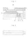
- FIG. 1 is a cross-sectional view illustrating a transparent display device in accordance with example embodiments.
- a transparent display device 100 may include a transparent base substrate 105, a semiconductor device, a display structure, an encapsulation layer 165, a protection layer 180, etc.
- the transparent base substrate 105 may support the elements of the transparent display device 100.
- the transparent base substrate 105 may include a polymer having a desired flexibility, and thus the transparent display device 100 may be a flexible transparent display device.
- the transparent base substrate 105 may include a polyimide-base material.
- an electron donor unit may be combined with adjacent nitrogen atoms of an imide unit contained in the polyimide-base material.
- the electron donor unit may include an aromatic ring such as benzene.
- the imide unit in the polyimide-base material may serve as an electron acceptor unit.
- a charge transfer complex (CTC) may be formed because of the molecular interaction between the electron donor unit and the electron acceptor unit. Accordingly, the transparent base substrate 105 may have enhanced heat resistance and improved mechanical strength.
- the charge transfer complex may absorb a light having a wavelength of about 560nm to about 580nm so that the transparent base substrate 105 may be a colored base substrate having, for example, a yellow color.
- the transparent base substrate 105 may serve as a substantially transparent polymer substrate. That is, the transparent polymer substrate may include a polyimide-base material.
- the semiconductor device may be disposed on the transparent base substrate 105.
- the semiconductor device may include a thin film transistor (TFT). Additionally, wirings electrically connected to the semiconductor device may be arranged on the transparent base substrate 105.
- the semiconductor device may include an active pattern 110, a gate insulation layer 115, a gate electrode 120, a source electrode 130 and a drain electrode 135.
- a barrier layer may be additionally disposed on the transparent base substrate 105.
- the barrier layer may have a structure in which silicon compound layers containing silicon oxide (SiOx) or silicon nitride (SiNx) may be stacked on the transparent base substrate 105.
- the barrier layer may prevent oxygen and/or moisture from being permeated into the transparent base substrate 105.
- a buffer layer (not illustrated) may be disposed on the barrier layer.
- the buffer layer may include a silicon compound, for example, silicon oxide, silicon nitride, silicon oxynitride (SiOxNy), etc.
- the buffer layer may have a single layer structure or a multilayer structure.
- the buffer layer may prevent the diffusion of impurities, metal ions and/or moisture toward the overlying structures.
- the active pattern 110 of the semiconductor device may be disposed on the transparent base substrate 105 or the buffer layer.
- the active pattern 110 may include polysilicon, amorphous silicon, partially crystallized silicon, microcrystal containing silicon, etc.
- the active pattern 110 may include oxide semiconductor.
- the gate insulation layer 115 may be disposed on the transparent base substrate 105 to substantially cover the active pattern 110.
- the gate insulation layer 115 may include a silicon compound, for example, silicon oxide, silicon nitride, silicon oxynitride, etc.
- the gate electrode 120 may be disposed on the gate insulation layer 115.
- the gate electrode 120 may be positioned on a portion of the gate insulation layer 115 under which the active pattern 110 is located.
- the gate electrode 120 may include metal, alloy, metal nitride, etc.
- the gate electrode 120 may include molybdenum (Mo), alloy containing molybdenum, aluminum (Al), alloy containing aluminum, aluminum nitride (AlNx), silver, alloy containing silver, tungsten (W), tungsten nitride (WNx), copper (Cu), alloy containing copper, nickel (Ni), titanium (Ti), titanium nitride (TiNx), platinum (Pt), tantalum (Ta), tantalum nitride (TaNx), etc.
- the gate electrode 120 may include a transparent conductive material such as indium tin oxide, indium zinc oxide, etc.
- An insulating interlayer 125 may be disposed on the gate insulation layer 115 and the gate electrode 120.
- the insulating interlayer 125 may include a silicon compound, for example, silicon oxide, silicon nitride, etc.
- the source electrode 130 and the drain electrode 135 may be disposed on the insulating interlayer 125.
- the source and the drain electrodes 130 and 135 may pass through the insulating interlayer 125 and the gate insulation layer 115, and then may contact the active pattern 110.
- Each of the source and the drain electrodes 130 and 135 may include metal, alloy, metal nitride, conductive metal oxide, etc.
- each of the source and the drain electrodes 130 and 135 may include a transparent conductive material.
- the wirings may be electrically connected to the semiconductor device.
- the wirings may include a scan line electrically connected to the gate electrode 120, and a data line electrically connected to the source electrode 130.
- An insulation layer 140 may be disposed on the insulating interlayer 125 to cover the semiconductor device and the wirings.
- the insulation layer 140 may include acryl-based resin, polyimide-based resin, epoxy-based resin, polyester-based resin, etc.
- the display structure may be disposed on the insulation layer 140.
- the display structure may include a first electrode 145, a display layer 155 and a second electrode 160.
- the first electrode 145 may be positioned on the insulation layer 140.
- the first electrode 145 may be electrically connected to the drain electrode 135.
- the first electrode 145 may pass through the insulation layer 140, and then may contact the drain electrode 135.
- the first electrode 145 may include metal, alloy, metal nitride, conductive metal oxide, etc.
- the first electrode 145 may serve as a reflective electrode or a transmissive electrode in accordance with the type of the transparent display device 100.
- a pixel defining layer 150 may be disposed the insulation layer 140.
- the pixel defining layer 150 may substantially cover a peripheral portion of the first electrode 145, and may define a display region, a pixel region or a luminescent region of the transparent display device 100.
- the pixel defining layer 150 may include photoresist, acryl-based resin, polyimide-based resin, polyamide-based resin, etc.
- the display layer 155 may be located on the first electrode 145.
- the display layer 155 may include an organic light emitting layer.
- the transparent display device 100 may be a transparent organic light emitting display device.
- the organic light emitting layer may additionally include a hole transfer layer (HTL), an electron transfer layer (ETL), etc.
- the display layer 155 may include a liquid crystal layer, and thus the transparent display device 100 may be a transparent liquid crystal display device.
- an alignment layer for the alignment of liquid crystal molecules may be disposed on the first electrode 145 and/or the second electrode 160.
- the display layer 155 extends on the pixel defining layer 150 from the first electrode 145 in FIG. 1 , the display layer 155 may be confined by a pixel opening of the pixel defining layer exposing the first electrode 145.
- the second electrode 160 may be disposed on the display layer 155.
- the second electrode 160 may extend onto the pixel defining layer 150.
- the second electrode 160 may include metal, metal nitride, transparent conductive metal oxide, etc.
- the encapsulation layer 165 may be disposed on the second electrode 160 to cover the display structure.
- the encapsulation layer 165 may substantially cover a front surface of the transparent display device 100.
- the encapsulation layer 165 may include a transparent organic material or a silicon-based material.
- the protection layer 180 may be disposed on the encapsulation layer 165 to protect the display structure.
- the protection layer 180 may include an adhesion film 170 and a protection film 175.
- At least one of the adhesion film 170 and the protection film 175 may contain a blue dye.
- the blue dye may include anthraquinone-based blue dye, azo-based blue dye, phthalocyanine-based blue dye, etc. These may be used alone or in a mixture thereof.
- the blue dye may selectively absorb a light having a wavelength of about 460nm to about 480nm.
- the adhesion film 170 may include a pressure sensitive adhesive (PSA).
- PSA pressure sensitive adhesive
- the adhesion film 170 may include a polymer resin formed by a polarization of the blue dye and a monomer.
- the adhesion film 170 may include an acryl-based resin combined with the blue dye.
- the protection film 175 may be attached to the front surface of the transparent display device 100 to prevent moisture and dusts from being permeated into the transparent display device 100 from an outside. Additionally, the protection film 175 may prevent the transparent display device 100 from damages, such as scratch.
- the protection film 175 may include the blue dye so that the protection film 175 and/or the adhesion film 170 may perform a color calibration of an image displayed on the transparent display device 100.
- the adhesion film 170 may calibrate a large yellow index caused by the charge transfer complex existing in the colored polymer substrate. For example, the blue color of the adhesion film 170 may be superimposed with the yellow color of the colored polymer substrate to achieve the transparency of the transparent base substrate 105. Therefore, the charge transfer complex may improve the mechanical strength and the heat resistance of the transparent base substrate 105 while enhancing transparency of the transparent base substrate 105 by the adhesion film 170.
- the transparent base substrate 105 when the transparent base substrate 105 is the transparent polymer substrate, it may have relatively low heat resistance and mechanical strength compared to the colored polymer substrate. Thus, the transparent base substrate 105 may be discolored such as yellowing by a thermal treatment when forming the active pattern 110 or a curing the elements such as an organic material. In this case, the adhesion film 170 may calibrate the yellowing of the transparent base substrate 105 to improve the transparency of the transparent base substrate 105.
- an amount of the blue dye may be properly adjusted to address the discoloration of the transparent base substrate 105.
- the protection layer 180 may additionally include blue pigment particles.
- the blue pigment particles may include phthalocyanine-based blue pigment particles, cobalt blue-based pigment particles, prussian blue-based pigment particles, turkey blue-based pigment particles, etc. These may be used alone or in a mixture thereof.
- the blue pigment particles may have an average diameter of about 10nm to about 100nm.
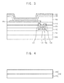
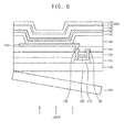
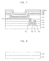
- FIGS. 2 through 7 are cross-sectional views illustrating a method of manufacturing a transparent display device in accordance with example embodiments.
- a transparent base substrate 105 may be attached on a carrier substrate 200.
- the carrier substrate 200 may include, for example, a glass substrate.
- the transparent base substrate 105 may be the above-described colored polymer substrate or the transparent polymer substrate.
- a semiconductor device and wirings may be formed on the transparent base substrate 105, and then a display structure may be formed over the semiconductor device and wirings.
- the semiconductor device may include an active pattern 110, a gate insulation layer 115, a gate electrode 120, a source electrode 130 and a drain electrode 135.
- the wirings may include a scan line, a data line, etc.
- a barrier layer may be formed on the transparent base substrate 105.
- the barrier layer may prevent permeation of moisture and/or oxygen into the transparent base substrate 105 from outside.
- the barrier layer may be formed of silicon oxide, silicon nitride, etc.
- a buffer layer may be formed on the barrier layer to prevent diffusion of impurities, metal ions and/or moisture into the overlying elements of the transparent display device.
- the buffer layer may be formed using silicon oxide, silicon nitride, silicon oxynitride, etc.
- the active pattern 110 may be formed on the buffer layer or and transparent base substrate 105.
- the active pattern 110 may be formed using polysilicon, amorphous silicon, partially crystallized silicon, silicon containing micro crystals, or oxide semiconductor such as indium zinc oxide, indium tin oxide, indium gallium zinc oxide, etc.
- the gate insulation layer 115 may be formed on the buffer layer or the transparent base substrate 105 to substantially cover the active pattern 110.
- the gate insulation layer 115 may be formed of silicon oxide, silicon nitride, silicon oxynitride, etc.
- the gate electrode 120 may be formed on the gate insulation layer 115.
- the gate electrode 120 may be located directly over the active pattern 110.
- the gate electrode 120 may be formed of metal, alloy, metal nitride, transparent conductive metal oxide, etc.
- An insulating interlayer 125 may be formed on the gate insulation layer 115 to cover the gate electrode 120.
- the insulating interlayer 125 may have a substantially level upper surface.
- the insulating interlayer 125 may be formed using silicon oxide, silicon nitride, silicon oxynitride, etc.
- the source and the drain electrodes 130 and 135 may be formed on the insulating interlayer 125. After forming contact holes exposing portions of the active pattern 110 through the insulating interlayer 125 and the gate insulation layer 115, the source and the drain electrodes 130 and 135 may be formed to substantially fill the contact holes. Each of the source and the drain electrodes 130 and 135 may be formed using metal, alloy, metal nitride, transparent conductive metal oxide, etc.
- An insulation layer 140 may be formed on the insulating layer 125 to cover the source and the drain electrodes 130 and 135.
- the insulation layer 140 may be formed using an acryl-based resin, a polyimide-based resin, an epoxy-based resin, a polyester-based resin etc.
- a display structure including a first electrode 145, a display layer 155 and a second electrode 160 may be formed in the insulation layer 140.
- the first electrode 145 may be formed on the insulation layer 140. After a hole exposing the drain electrode 135 may be formed through the insulation layer 140, the first electrode 145 may be formed in the hole to contact the drain electrode 135.
- the first electrode 145 may be formed of a material either reflective or transmissive depending on the type of the transparent display device.
- a pixel defining layer 150 may be formed on the first electrode 145 and the insulation layer 140.
- the pixel defining layer 150 may be formed of polyimide-based resin, photoresist, polyacryl-based resin, polyamide-based resin, acryl-based resin, etc.
- a pixel opening may be formed through pixel defining layer 150. The pixel opening may partially expose the first electrode 145.
- the display layer 155 may be formed on the exposed first electrode 145.
- the display layer 155 may include an organic light emitting layer or a liquid crystal layer in accordance with the type of the transparent display device.
- the second electrode 160 may be formed on the display layer 155 and the pixel defining layer 150.
- the second electrode 160 may serve as a common electrode between adjacent pixels.
- the second electrode 160 may also be formed of a material either reflective or transmissive depending on the type of the transparent display device.
- an encapsulation layer 165 (see FIG. 1 ) may be formed on the second electrode 160.
- the encapsulation layer 165 may cover the display structure.
- the encapsulation layer 165 may be substantially opposed to the transparent base substrate 105.
- a protection layer 180 may be provided.
- an adhesion film 170 may be formed on a protection film 175 by coating an adhesion composition containing a blue dye on a surface of the protection film 175.
- the adhesion composition may include the blue dye, a monomer such as an acryl-based monomer, a polymerization initiator and a solvent.
- the blue dye and the monomer may be combined and/or polymerized to form a polymer resin combined with the blue dye.
- an acryl-based resin combined with the blue dye may be used to form the adhesion film 170.
- Examples of the acryl-based monomer may include methacrylic acid, acrylic acid, methyl methacrylate, benzyl methacrylate, 2- hydroxyethyl methacrylate, aryl methacrylate, glycidyl methacrylate, etc. These may be used alone or in a mixture thereof.
- blue dye may include a compound represented by the following Formula I:
- R indicates a reactive functional group such as an alkene group (e.g. a C2-C6 alkene group), and can combine with the acryl-based monomer by an addition reaction or a condension reaction.
- the acryl-based resin combined with the blue dye may be obtained by a reaction between the acryl-based monomer and the compound of Formula I.
- the acryl-based resin combined with the blue dye may be represented by the following Formula II:
- x and y are positive integers, and the sum of x and y is in a range of about 2 to about 1,000.
- the acryl-based resin combined with the blue dye may be of about 3 to about 20 percent by weight based on a total weight of the adhesion composition.
- the adhesion film 170 formed from the adhesion composition may have low mechanical strength.
- the adhesion film 170 may not be uniform in thickness.
- the polymerization initiator may generate radicals by a heat or a light, and may accelerate a polymerization reaction between the monomer and the blue dye.
- the polymerization initiator may include an azo-based compound, azonitril-based compound, an azoamide-based compound, an azoamidine-based compound, a maxro-azo-based compound, an acetophenone-based compound, a benzophenone-based compound, an oxime-based compound, etc. These may be used alone or in a mixture thereof.
- the polymerization initiator may have a content of about 0.5 to about 5 percent by weight based on the total weight of the adhesion composition. When the content of the polymerization initiator is below 0.5 percent by weight, the polymerization reaction may not be able to be properly occurred. When the content of the polymerization initiator is above 5 percent by weight, the polymerization initiator may not be desirably controlled in the adhesion composition.
- the solvent may include propyleneglycolmonomethylether acetate, ethylethoxypropionate, cyclohexanone, dipropyleneglycolmonomethylether acetate, n-butylacetate, isobutylacetate, ethyleneglycolmonomethylacetate, ethyleneglycol n-butylacetate, diethyleneglycoldimethylether, dipropyleneglycolmonomethylacetate, diethyleneglycolmethylether, dipropyleneglycol n-butylether, tripropyleneglycol n-butylether, tripropyleneglycolmethylether, propyleneglycolmethylether acetate, propyleneglycoldiacetate, 3-ethoxy methyl propionate, methanol, ethanol, methylcellusolvemonomethylether, ethylcellusolve acetate, diethyleneglycolmonomethylether, methylethylketone, 4-hydroxy-4-methyl-2-p
- the adhesion composition may additionally include blue pigment particles.
- blue pigment particles may enhance the color calibration of the adhesion film 170.
- the blue pigment particles may include phthalocyanine-based blue pigment particles, cobalt blue-based pigment particles, prussian blue-based pigment particles, turkey blue-based pigment particles, etc. These may be used alone or in a mixture thereof.
- the blue pigment particles may have an average diameter of about 10nm to about 100nm.
- the blue pigment particles may have a content of about 1.0 to about 10.0 percent by weight based on the total adhesion composition. When the content of the blue pigment particles is above 10 percent by weight, the adhesion composition may not be properly cured.
- the adhesion composition may additionally include additives such as a cross-linking agent, a surfactant, etc.
- the cross-linking agent may accelerate a cross-linking between the acryl-based monomer and the blue dye.
- the cross-linking agent may include an inorganic chelating agent or an organic chelating agent.
- the surfactant may include FZ-2110 or FZ-2122 (Dow Corning Co., U.S.A.), or BYK-345 (BYK Co., U.S.A.).
- the polymer resin combined with the blue dye may be obtained from the adhesion composition according to example embodiments.
- the blue dye may be desirably confined in the adhesion film 170 by directly combining the blue dye with the monomer, so that the adhesion film 170 may have improved reliability.
- the blue dye may be contained in the polymer resin to prevent the localization of the blue dye. Therefore, the transparent base substrate 105 may have an entirely uniform transparency because of uniform distribution of the blue dye in the adhesion film 170.
- the adhesion composition may be cured by a thermal treatment of a UV irradiation after attaching the adhesion film 170 to the surface of the protection film 175.
- the blue dye and the monomer may be combined and/or condensed to obtain the polymer resin combined with the blue dye.
- the blue dye may be distributed in the adhesion composition.
- the monomers may be polymerized and/or co-polymerized to obtain the polymer resin combined with the blue dye.
- the protection layer 180 may be attached to the encapsulation layer 165.
- the protection layer 180 may prevent the underlying structures from impurities, moisture, scratch, etc.
- the protection film 175 may include a transparent resin such as polyethylene terephthalate (PET), polycarbonate (PC), polyvinyl chloride (PVC), etc.
- the protection film 175 may be formed using a transparent resin containing the above-described blue dye. Accordingly, the protection film 175 may also perform the color calibration of the image as the adhesion film 170.
- an optical layer and an additional transparent substrate may be provided on the protection layer 180.
- the carrier substrate 200 may be separated from the transparent base substrate 105.
- the carrier substrate 200 may be detached from the transparent base substrate 105 by irradiating a laser onto an interface between the carrier substrate 200 and the transparent base substrate 105.
- the carrier substrate 200 may be separated by applying mechanical force to the interface between the carrier substrate 200 and the transparent base substrate 105.
- the carrier substrate 200 may be separated after forming the adhesion film 170 and the protection film 175 on the encapsulation layer 165. In some example embodiments, the carrier substrate 200 may be separated from the transparent base substrate 105 before forming the protection layer 180 on the encapsulation layer 165.
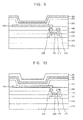
- FIGS. 8 to 14 are cross-sectional views illustrating a method of manufacturing a transparent display device in accordance with some example embodiments.
- FIGS. 8 to 14 detailed descriptions of processes and/or elements substantially the same as the processes and/or the elements described with reference to FIGS. 2 to 7 will be omitted.
- a transparent base substrate 205 such as a colored polymer substrate or a transparent polymer substrate may be formed on a carrier substrate 300 such as a glass substrate.
- a semiconductor device and wirings may be formed on the transparent base substrate 205.
- the semiconductor device may include an active pattern 210, a gate insulation layer 215, a gate electrode 220, a source electrode 230 and a drain electrode 235.
- the wirings may be electrically connected to the semiconductor device.
- a barrier layer may be formed on the transparent base substrate 205 so as to prevent the permeation of moisture and/or oxygen into the transparent base substrate 205.
- the barrier layer may be formed using silicon oxide, silicon nitride, etc.
- a buffer layer may be formed on the barrier layer to prevent the diffusion of impurities, metal ions and/or moisture into the overlying elements of the transparent display device.
- the buffer layer may be formed using silicon oxide, silicon nitride, silicon oxynitride, etc.
- the active pattern 210 may be formed on the buffer layer or and transparent base substrate 205 using polysilicon, amorphous silicon, partially crystallized silicon, silicon containing micro crystals, or oxide semiconductor such as indium zinc oxide, indium tin oxide, indium gallium zinc oxide, etc.
- the gate insulation layer 215 may be formed on the buffer layer or the transparent base substrate 205 to substantially cover the active pattern 210.
- the gate insulation layer 215 may be formed using silicon oxide, silicon nitride, silicon oxynitride, etc.
- the gate electrode 220 may be formed on the gate insulation layer 215 using metal, alloy, metal nitride, transparent conductive metal oxide, etc.
- the gate electrode 120 may be located directly over the active pattern 210.
- An insulating interlayer 225 may be formed on the gate insulation layer 215 to cover the gate electrode 220 using silicon oxide, silicon nitride, silicon oxynitride, etc.
- the insulating interlayer 225 may have a substantially flat upper surface.
- the source and the drain electrodes 230 and 235 may be formed on the insulating interlayer 225.
- the source and the drain electrodes 230 and 235 may pass through the insulating interlayer 225 and the gate insulation layer 215, and then may make contact a source region and a drain region of the active pattern 210, respectively.
- Each of the source and the drain electrodes 230 and 235 may be formed using metal, alloy, metal nitride, transparent conductive metal oxide, etc.
- An insulation layer 240 may be formed on the insulating layer 225 to cover the source and the drain electrodes 230 and 235 using an acryl-based resin, a polyimide-based resin, an epoxy-based resin, a polyester-based resin etc.
- a display structure including a first electrode 245, a display layer 255 and a second electrode 260 may be formed in the insulation layer 240.
- the first electrode 245 may pass through the insulation layer 240 and may contact the drain electrode 235.
- the first electrode 245 may be formed using a material having a reflectivity or a transmittance in accordance with the emission type of the transparent display device.
- a pixel defining layer 250 may be formed on the first electrode 245 and the insulation layer 240 using polyimide-based resin, photoresist, polyacryl-based resin, polyamide-based resin, acryl-based resin, etc.
- a pixel opening partially exposing the first electrode 245 may be formed through pixel defining layer 250.
- the display layer 255 may be formed on the exposed first electrode 245.
- the display layer 255 may include an organic light emitting layer or a liquid crystal layer in accordance with the type of the transparent display device.
- the second electrode 260 may be formed on the display layer 255 and the pixel defining layer 250 using a material having a reflectivity or a transmittance in accordance with the emission type of the transparent display device.
- the second electrode 260 may serve as a common electrode between adjacent pixels.
- an encapsulation layer 265 may be formed on the second electrode 260 to protect the display structure.
- an adhesion film 270 may be formed on the encapsulation layer 265 by coating an adhesion composition on the encapsulation layer 265.
- the adhesion composition may include a blue dye, a monomer such as an acryl-based monomer, a polymerization initiator and a solvent.
- the adhesion film 270 may be obtained by curing the adhesion composition by means of a thermal treatment or a UV irradiation after coating the adhesion composition onto the encapsulation layer 265.
- the blue dye and the monomer may be combined and/or polymerized to obtain a polymer resin combined with the blue dye.
- the blue dye may be distributed in the adhesion composition.
- the monomers may be polymerized and/or co- polymerized to obtain the polymer resin combined with the blue dye.
- a protection film 275 may be formed on the adhesion film 270 so as to prevent the underlying structures from impurities, moisture, scratch, etc.
- a protection layer 280 may be provided on the encapsulation layer 265. That is, the protection layer 280 may include a protection film 275 and adhesion film 270.
- the protection film 275 may include a transparent resin such as polyethylene terephthalate, polycarbonate, polyvinyl chloride, etc.
- the protection film 275 may be formed of a transparent resin containing the above-described blue dye, so that the protection film 275 may also perform the color calibration of the image as adhesion film 270.
- an optical layer and an additional transparent substrate may be provided on the protection layer 280.
- the carrier substrate 300 may be separated from the transparent base substrate 205 by irradiating a laser onto an interface between the carrier substrate 300 and the transparent base substrate 305, or by applying mechanical force to the interface between the carrier substrate 300 and the transparent base substrate 305.
- the adhesion film and/or the protection film containing the blue dye may improve the transparency of the transparent base substrate by calibrating discoloration of the transparent base substrate.
- the transparent display device including the protection layer may ensure enhanced transparency.
- the transparent base substrate may have enhanced mechanical strength and increased heat resistance because of the charge transfer complex, so that the transparent display device may also have enhanced mechanical strength and increased heat resistance.
- the display apparatuses may ensure enhanced characteristics, for example, improved mechanical strength, increased transparency, increased heat resistance, etc.
Landscapes
- Engineering & Computer Science (AREA)
- Physics & Mathematics (AREA)
- Manufacturing & Machinery (AREA)
- Chemical & Material Sciences (AREA)
- Materials Engineering (AREA)
- Optics & Photonics (AREA)
- Spectroscopy & Molecular Physics (AREA)
- Microelectronics & Electronic Packaging (AREA)
- Electroluminescent Light Sources (AREA)
- Devices For Indicating Variable Information By Combining Individual Elements (AREA)
Abstract
Description
- The invention relates to transparent display devices and methods of manufacturing transparent display devices.
- Recently, a transparent display device has been rapidly developed. In the conventional transparent display device, an image of an object before or after a transparent region of the transparent display device may be recognized by a user when the transparent display device operates in an "OFF" state. In an "ON" state of the transparent display device, an image may be displayed in a pixel region of the transparent display device.
- In the conventional transparent display device, a base substrate may be formed using polyimide so as to improve the flexibility of the transparent display device. However, such a base substrate may not have a desired level of heat resistance and mechanical strength. So the conventional transparent display device may provide neither desired level of transparency nor proper mechanical strength.
- The above information disclosed in this Background section is only for enhancement of understanding of the background of the inventive concept, and, therefore, it may contain information that does not form the prior art that is already known in this country to a person of ordinary skill in the art.
- The invention provides transparent display devices including transparent base substrates to enhance transparencies and mechanical strengths.
- The invention provides a method of manufacturing transparent display devices including transparent base substrates to enhance transparencies and mechanical strengths
- Additional aspects will be set forth in the detailed description which follows, and, in part, will be apparent from the disclosure, or may be learned by practice of the inventive concept.
- According to one aspect of the invention, there is provided a transparent organic light emitting display device comprising a transparent base substrate, a semiconductor device disposed on the transparent base substrate, a display structure electrically connected to the semiconductor device, and a protection layer comprising a blue dye disposed on the display structure.
- In example embodiments, the protection layer may comprise an adhesion film and a protection film. The blue dye may be contained in at least one of the adhesion film and the protection film. For example, the adhesion film may comprise a pressure sensitive adhesive (PSA) containing the blue dye.
- In example embodiments, the adhesion film may comprise a polymer polymerized with a monomer and the blue dye. The adhesion film may comprise an acryl-based resin combined with the blue dye.
- In some example embodiments, the transparent organic light emitting display device may additionally comprise an encapsulation layer covering the display structure. The adhesion film may be attached to the encapsulation layer.
- In example embodiments, the blue dye may comprise anthraquinone-based blue dye, azo-based blue dye and/or phthalocyanine-based blue dye.
- In some example embodiments, the protection layer may comprise blue pigment particles.
- In example embodiments, the transparent base substrate may be a transparent polymer substrate or a colored polymer substrate. For example, the colored polymer substrate may comprise a polyimide-based material containing an electron donor unit combined between adjacent imide units, and a charge transfer complex formed by a molecular interaction between the electron donor unit and the imide unit serving as an electron acceptor unit. The colored polymer substrate may have a yellow color. Additionally, the transparent base substrate may comprise a transparent polyimide-based material.
- In example embodiments, the display structure comprises an organic light emitting layer or a liquid crystal layer. In this case, the display structure may comprise a first electrode electrically connected to the semiconductor device, and a second electrode opposed to the first electrode. The organic light emitting layer or the liquid crystal layer may be disposed between the first electrode and the second electrode.
- According to one aspect of the invention, there is provided a method of manufacturing a transparent organic light emitting display device. In the method, a transparent base substrate is formed on a carrier substrate. A semiconductor device is formed on a transparent base substrate. An insulation layer is formed on the transparent base substrate to substantially cover the semiconductor device. A display structure is formed on the insulation layer. The display structure is electrically connected to the semiconductor device. An encapsulation layer may be formed to substantially cover the display structure. A protection layer comprising a blue dye is formed on the encapsulation layer.
- When forming the protection layer according to example embodiments, an adhesion film may be formed on a surface of a protection film. The blue dye may be contained in the adhesion film and/or the protection film.
- In some example embodiments, the adhesion film may be attached to the encapsulation layer.
- When forming the adhesion film according to example embodiments, an adhesion composition containing the blue dye, a monomer, a polymerization initiator and a solvent may be coated on the surface of the protection film. Here, a polymer resin may be formed by a polymerization of the blue dye and the monomer. The monomer may include an acryl-based monomer and the polymer resin may include an acryl-based resin combined with the blue dye. Examples of the acryl-based monomer may include methacrylic acid, acrylic acid, methyl methacrylate, benzyl methacrylate, 2-hydroxyethyl methacrylate, aryl methacrylate and/or glycidyl methacrylate.
- When forming the protection layer according to some example embodiments, an adhesion film may be formed on an upper surface of the encapsulation layer. A protection film may be formed on the adhesion film. Here, the blue dye may be contained in at least one of the adhesion film and the protection film.
- In the formation of the adhesion film according to some example embodiments, an adhesion composition comprising the blue dye, a monomer, a polymerization initiator and a solvent may be coated onto the upper surface of the encapsulation layer. Here, a polymer resin may be formed by a polymerization of the blue dye and the monomer.
- In example embodiments, the transparent base substrate may be attached on a carrier substrate, and then the carrier substrate may be separated from transparent base substrate after forming the encapsulation layer. Alternatively, the carrier substrate may be separated after forming the protection layer.
- According to example embodiments, the adhesion film and/or the protection film comprising the blue dye may improve the transparency of the transparent base substrate by calibrating discoloration of the transparent base substrate. Thus, the transparent display device including the protection layer may provide enhanced transparency. Moreover, the transparent base substrate may have enhanced mechanical strength and increased heat resistance because of the charge transfer complex, so that the transparent display device may also have enhanced mechanical strength and increased heat resistance.
- The foregoing general description and the following detailed description are exemplary and explanatory and are intended to provide further explanation of the claimed subject matter.
- The accompanying drawings, which are included to provide a further understanding of the inventive concept, and are incorporated in and constitute a part of this specification, illustrate exemplary embodiments of the inventive concept, and, together with the description, serve to explain principles of the inventive concept.
-
FIG. 1 is a cross-sectional view illustrating a transparent display device in accordance with example embodiments. -
FIGS. 2 through 7 are cross-sectional views illustrating a method of manufacturing a transparent display device in accordance with example embodiments. -
FIGS. 8 through 14 are cross-sectional views illustrating a method of manufacturing a transparent display device in accordance with some example embodiments. -
FIG. 1 is a cross-sectional view illustrating a transparent display device in accordance with example embodiments. - Referring to
FIG. 1 , atransparent display device 100 may include atransparent base substrate 105, a semiconductor device, a display structure, anencapsulation layer 165, aprotection layer 180, etc. - The
transparent base substrate 105 may support the elements of thetransparent display device 100. For example, thetransparent base substrate 105 may include a polymer having a desired flexibility, and thus thetransparent display device 100 may be a flexible transparent display device. - In example embodiments, the
transparent base substrate 105 may include a polyimide-base material. Here, an electron donor unit may be combined with adjacent nitrogen atoms of an imide unit contained in the polyimide-base material. Examples of the electron donor unit may include an aromatic ring such as benzene. The imide unit in the polyimide-base material may serve as an electron acceptor unit. A charge transfer complex (CTC) may be formed because of the molecular interaction between the electron donor unit and the electron acceptor unit. Accordingly, thetransparent base substrate 105 may have enhanced heat resistance and improved mechanical strength. The charge transfer complex may absorb a light having a wavelength of about 560nm to about 580nm so that thetransparent base substrate 105 may be a colored base substrate having, for example, a yellow color. - In some example embodiments, functional groups having a relatively high electronegativity such as -CF3 or -SiO2 may be introduced between the imide units or into the imide unit. This may decrease the electron density of the imide unit and suppress the formation of the charge transfer complex. Further, a relatively bulky functional group containing a plurality of aromatic rings may be introduced between the imide units or into the imide unit, which may inhibit the formation of the charge transfer complex. Accordingly, the
transparent base substrate 105 may serve as a substantially transparent polymer substrate. That is, the transparent polymer substrate may include a polyimide-base material. - The semiconductor device may be disposed on the
transparent base substrate 105. The semiconductor device may include a thin film transistor (TFT). Additionally, wirings electrically connected to the semiconductor device may be arranged on thetransparent base substrate 105. In some example embodiments, the semiconductor device may include anactive pattern 110, agate insulation layer 115, agate electrode 120, asource electrode 130 and adrain electrode 135. - Although it is not shown, a barrier layer may be additionally disposed on the
transparent base substrate 105. The barrier layer may have a structure in which silicon compound layers containing silicon oxide (SiOx) or silicon nitride (SiNx) may be stacked on thetransparent base substrate 105. The barrier layer may prevent oxygen and/or moisture from being permeated into thetransparent base substrate 105. - In example embodiments, a buffer layer (not illustrated) may be disposed on the barrier layer. The buffer layer may include a silicon compound, for example, silicon oxide, silicon nitride, silicon oxynitride (SiOxNy), etc. The buffer layer may have a single layer structure or a multilayer structure. The buffer layer may prevent the diffusion of impurities, metal ions and/or moisture toward the overlying structures.
- The
active pattern 110 of the semiconductor device may be disposed on thetransparent base substrate 105 or the buffer layer. Theactive pattern 110 may include polysilicon, amorphous silicon, partially crystallized silicon, microcrystal containing silicon, etc. Alternatively, theactive pattern 110 may include oxide semiconductor. - The
gate insulation layer 115 may be disposed on thetransparent base substrate 105 to substantially cover theactive pattern 110. Thegate insulation layer 115 may include a silicon compound, for example, silicon oxide, silicon nitride, silicon oxynitride, etc. - The
gate electrode 120 may be disposed on thegate insulation layer 115. Thegate electrode 120 may be positioned on a portion of thegate insulation layer 115 under which theactive pattern 110 is located. Thegate electrode 120 may include metal, alloy, metal nitride, etc. For example, thegate electrode 120 may include molybdenum (Mo), alloy containing molybdenum, aluminum (Al), alloy containing aluminum, aluminum nitride (AlNx), silver, alloy containing silver, tungsten (W), tungsten nitride (WNx), copper (Cu), alloy containing copper, nickel (Ni), titanium (Ti), titanium nitride (TiNx), platinum (Pt), tantalum (Ta), tantalum nitride (TaNx), etc. Alternatively, thegate electrode 120 may include a transparent conductive material such as indium tin oxide, indium zinc oxide, etc. - An insulating
interlayer 125 may be disposed on thegate insulation layer 115 and thegate electrode 120. The insulatinginterlayer 125 may include a silicon compound, for example, silicon oxide, silicon nitride, etc. - The
source electrode 130 and thedrain electrode 135 may be disposed on the insulatinginterlayer 125. The source and thedrain electrodes interlayer 125 and thegate insulation layer 115, and then may contact theactive pattern 110. Each of the source and thedrain electrodes drain electrodes - The wirings may be electrically connected to the semiconductor device. For example, the wirings may include a scan line electrically connected to the
gate electrode 120, and a data line electrically connected to thesource electrode 130. - An
insulation layer 140 may be disposed on the insulatinginterlayer 125 to cover the semiconductor device and the wirings. For example, theinsulation layer 140 may include acryl-based resin, polyimide-based resin, epoxy-based resin, polyester-based resin, etc. - The display structure may be disposed on the
insulation layer 140. The display structure may include afirst electrode 145, adisplay layer 155 and asecond electrode 160. - The
first electrode 145 may be positioned on theinsulation layer 140. Thefirst electrode 145 may be electrically connected to thedrain electrode 135. For example, thefirst electrode 145 may pass through theinsulation layer 140, and then may contact thedrain electrode 135. Thefirst electrode 145 may include metal, alloy, metal nitride, conductive metal oxide, etc. Thefirst electrode 145 may serve as a reflective electrode or a transmissive electrode in accordance with the type of thetransparent display device 100. - A
pixel defining layer 150 may be disposed theinsulation layer 140. Thepixel defining layer 150 may substantially cover a peripheral portion of thefirst electrode 145, and may define a display region, a pixel region or a luminescent region of thetransparent display device 100. For example, thepixel defining layer 150 may include photoresist, acryl-based resin, polyimide-based resin, polyamide-based resin, etc. - The
display layer 155 may be located on thefirst electrode 145. In example embodiments, thedisplay layer 155 may include an organic light emitting layer. Here, thetransparent display device 100 may be a transparent organic light emitting display device. The organic light emitting layer may additionally include a hole transfer layer (HTL), an electron transfer layer (ETL), etc. - In some example embodiments, the
display layer 155 may include a liquid crystal layer, and thus thetransparent display device 100 may be a transparent liquid crystal display device. In this case, an alignment layer for the alignment of liquid crystal molecules may be disposed on thefirst electrode 145 and/or thesecond electrode 160. - Although the
display layer 155 extends on thepixel defining layer 150 from thefirst electrode 145 inFIG. 1 , thedisplay layer 155 may be confined by a pixel opening of the pixel defining layer exposing thefirst electrode 145. - The
second electrode 160 may be disposed on thedisplay layer 155. For example, thesecond electrode 160 may extend onto thepixel defining layer 150. Thesecond electrode 160 may include metal, metal nitride, transparent conductive metal oxide, etc. - The
encapsulation layer 165 may be disposed on thesecond electrode 160 to cover the display structure. For example, theencapsulation layer 165 may substantially cover a front surface of thetransparent display device 100. Theencapsulation layer 165 may include a transparent organic material or a silicon-based material. - The
protection layer 180 may be disposed on theencapsulation layer 165 to protect the display structure. In example embodiments, theprotection layer 180 may include anadhesion film 170 and aprotection film 175. At least one of theadhesion film 170 and theprotection film 175 may contain a blue dye. Examples of the blue dye may include anthraquinone-based blue dye, azo-based blue dye, phthalocyanine-based blue dye, etc. These may be used alone or in a mixture thereof. The blue dye may selectively absorb a light having a wavelength of about 460nm to about 480nm. - The
adhesion film 170 may include a pressure sensitive adhesive (PSA). Alternatively, theadhesion film 170 may include a polymer resin formed by a polarization of the blue dye and a monomer. For example, theadhesion film 170 may include an acryl-based resin combined with the blue dye. - The
protection film 175 may be attached to the front surface of thetransparent display device 100 to prevent moisture and dusts from being permeated into thetransparent display device 100 from an outside. Additionally, theprotection film 175 may prevent thetransparent display device 100 from damages, such as scratch. In example embodiments, theprotection film 175 may include the blue dye so that theprotection film 175 and/or theadhesion film 170 may perform a color calibration of an image displayed on thetransparent display device 100. - As described above, when the
transparent base substrate 105 is the colored polymer substrate having the yellow color, theadhesion film 170 may calibrate a large yellow index caused by the charge transfer complex existing in the colored polymer substrate. For example, the blue color of theadhesion film 170 may be superimposed with the yellow color of the colored polymer substrate to achieve the transparency of thetransparent base substrate 105. Therefore, the charge transfer complex may improve the mechanical strength and the heat resistance of thetransparent base substrate 105 while enhancing transparency of thetransparent base substrate 105 by theadhesion film 170. - In some example embodiments, when the
transparent base substrate 105 is the transparent polymer substrate, it may have relatively low heat resistance and mechanical strength compared to the colored polymer substrate. Thus, thetransparent base substrate 105 may be discolored such as yellowing by a thermal treatment when forming theactive pattern 110 or a curing the elements such as an organic material. In this case, theadhesion film 170 may calibrate the yellowing of thetransparent base substrate 105 to improve the transparency of thetransparent base substrate 105. - According to example embodiments, an amount of the blue dye may be properly adjusted to address the discoloration of the
transparent base substrate 105. In some example embodiments, theprotection layer 180 may additionally include blue pigment particles. Examples of the blue pigment particles may include phthalocyanine-based blue pigment particles, cobalt blue-based pigment particles, prussian blue-based pigment particles, turkey blue-based pigment particles, etc. These may be used alone or in a mixture thereof. For example, the blue pigment particles may have an average diameter of about 10nm to about 100nm. -
FIGS. 2 through 7 are cross-sectional views illustrating a method of manufacturing a transparent display device in accordance with example embodiments. - Referring to
FIG. 2 , atransparent base substrate 105 may be attached on acarrier substrate 200. Thecarrier substrate 200 may include, for example, a glass substrate. Thetransparent base substrate 105 may be the above-described colored polymer substrate or the transparent polymer substrate. - Referring to
FIG. 3 , a semiconductor device and wirings may be formed on thetransparent base substrate 105, and then a display structure may be formed over the semiconductor device and wirings. The semiconductor device may include anactive pattern 110, agate insulation layer 115, agate electrode 120, asource electrode 130 and adrain electrode 135. The wirings may include a scan line, a data line, etc. - Although it is not illustrated, a barrier layer may be formed on the
transparent base substrate 105. The barrier layer may prevent permeation of moisture and/or oxygen into thetransparent base substrate 105 from outside. The barrier layer may be formed of silicon oxide, silicon nitride, etc. Additionally, a buffer layer may be formed on the barrier layer to prevent diffusion of impurities, metal ions and/or moisture into the overlying elements of the transparent display device. The buffer layer may be formed using silicon oxide, silicon nitride, silicon oxynitride, etc. - The
active pattern 110 may be formed on the buffer layer or andtransparent base substrate 105. Theactive pattern 110 may be formed using polysilicon, amorphous silicon, partially crystallized silicon, silicon containing micro crystals, or oxide semiconductor such as indium zinc oxide, indium tin oxide, indium gallium zinc oxide, etc. - The
gate insulation layer 115 may be formed on the buffer layer or thetransparent base substrate 105 to substantially cover theactive pattern 110. Thegate insulation layer 115 may be formed of silicon oxide, silicon nitride, silicon oxynitride, etc. - The
gate electrode 120 may be formed on thegate insulation layer 115. Thegate electrode 120 may be located directly over theactive pattern 110. Thegate electrode 120 may be formed of metal, alloy, metal nitride, transparent conductive metal oxide, etc. - An insulating
interlayer 125 may be formed on thegate insulation layer 115 to cover thegate electrode 120. The insulatinginterlayer 125 may have a substantially level upper surface. The insulatinginterlayer 125 may be formed using silicon oxide, silicon nitride, silicon oxynitride, etc. - The source and the
drain electrodes interlayer 125. After forming contact holes exposing portions of theactive pattern 110 through the insulatinginterlayer 125 and thegate insulation layer 115, the source and thedrain electrodes drain electrodes - An
insulation layer 140 may be formed on the insulatinglayer 125 to cover the source and thedrain electrodes insulation layer 140 may be formed using an acryl-based resin, a polyimide-based resin, an epoxy-based resin, a polyester-based resin etc. - A display structure including a
first electrode 145, adisplay layer 155 and asecond electrode 160 may be formed in theinsulation layer 140. - The
first electrode 145 may be formed on theinsulation layer 140. After a hole exposing thedrain electrode 135 may be formed through theinsulation layer 140, thefirst electrode 145 may be formed in the hole to contact thedrain electrode 135. Thefirst electrode 145 may be formed of a material either reflective or transmissive depending on the type of the transparent display device. - A
pixel defining layer 150 may be formed on thefirst electrode 145 and theinsulation layer 140. Thepixel defining layer 150 may be formed of polyimide-based resin, photoresist, polyacryl-based resin, polyamide-based resin, acryl-based resin, etc. A pixel opening may be formed throughpixel defining layer 150. The pixel opening may partially expose thefirst electrode 145. - The
display layer 155 may be formed on the exposedfirst electrode 145. Thedisplay layer 155 may include an organic light emitting layer or a liquid crystal layer in accordance with the type of the transparent display device. - The
second electrode 160 may be formed on thedisplay layer 155 and thepixel defining layer 150. Thesecond electrode 160 may serve as a common electrode between adjacent pixels. Thesecond electrode 160 may also be formed of a material either reflective or transmissive depending on the type of the transparent display device. - Referring to
FIG. 3 again, an encapsulation layer 165 (seeFIG. 1 ) may be formed on thesecond electrode 160. Theencapsulation layer 165 may cover the display structure. Theencapsulation layer 165 may be substantially opposed to thetransparent base substrate 105. - Referring to
FIG. 4 , aprotection layer 180 may be provided. In forming of theprotection layer 180 according to example embodiments, anadhesion film 170 may be formed on aprotection film 175 by coating an adhesion composition containing a blue dye on a surface of theprotection film 175. The adhesion composition may include the blue dye, a monomer such as an acryl-based monomer, a polymerization initiator and a solvent. The blue dye and the monomer may be combined and/or polymerized to form a polymer resin combined with the blue dye. When the acryl-based monomer is used, an acryl-based resin combined with the blue dye may be used to form theadhesion film 170. - Examples of the acryl-based monomer may include methacrylic acid, acrylic acid, methyl methacrylate, benzyl methacrylate, 2- hydroxyethyl methacrylate, aryl methacrylate, glycidyl methacrylate, etc. These may be used alone or in a mixture thereof.
- Examples of the blue dye may include a compound represented by the following Formula I:

- In the above Formula I, R indicates a reactive functional group such as an alkene group (e.g. a C2-C6 alkene group), and can combine with the acryl-based monomer by an addition reaction or a condension reaction. For example, the acryl-based resin combined with the blue dye may be obtained by a reaction between the acryl-based monomer and the compound of Formula I. When R is -CH=CH2 in the above Formula I, the acryl-based resin combined with the blue dye may be represented by the following Formula II:

- In the above Formula II, x and y are positive integers, and the sum of x and y is in a range of about 2 to about 1,000.
- In some example embodiments, the acryl-based resin combined with the blue dye may be of about 3 to about 20 percent by weight based on a total weight of the adhesion composition. When the content of the acryl-based resin combined with the blue dye is below about 3 percent by weight, the
adhesion film 170 formed from the adhesion composition may have low mechanical strength. When the content of the acryl-based resin combined with the blue dye is above 20 percent by weight, theadhesion film 170 may not be uniform in thickness. - The polymerization initiator may generate radicals by a heat or a light, and may accelerate a polymerization reaction between the monomer and the blue dye. For example, the polymerization initiator may include an azo-based compound, azonitril-based compound, an azoamide-based compound, an azoamidine-based compound, a maxro-azo-based compound, an acetophenone-based compound, a benzophenone-based compound, an oxime-based compound, etc. These may be used alone or in a mixture thereof.
- The polymerization initiator may have a content of about 0.5 to about 5 percent by weight based on the total weight of the adhesion composition. When the content of the polymerization initiator is below 0.5 percent by weight, the polymerization reaction may not be able to be properly occurred. When the content of the polymerization initiator is above 5 percent by weight, the polymerization initiator may not be desirably controlled in the adhesion composition.
- Examples of the solvent may include propyleneglycolmonomethylether acetate, ethylethoxypropionate, cyclohexanone, dipropyleneglycolmonomethylether acetate, n-butylacetate, isobutylacetate, ethyleneglycolmonomethylacetate, ethyleneglycol n-butylacetate, diethyleneglycoldimethylether, dipropyleneglycolmonomethylacetate, diethyleneglycolmethylether, dipropyleneglycol n-butylether, tripropyleneglycol n-butylether, tripropyleneglycolmethylether, propyleneglycolmethylether acetate, propyleneglycoldiacetate, 3-ethoxy methyl propionate, methanol, ethanol, methylcellusolvemonomethylether, ethylcellusolve acetate, diethyleneglycolmonomethylether, methylethylketone, 4-hydroxy-4-methyl-2-pentanone, 2-hydroxy-2-methylethylproprionate, etc. These may be used alone or in a mixture thereof. The solvent may have a content of about 75 to about 95 percent by weight based on the total weight of the adhesion composition.
- In some example embodiments, the adhesion composition may additionally include blue pigment particles. Such blue pigment particles may enhance the color calibration of the
adhesion film 170. Examples of the blue pigment particles may include phthalocyanine-based blue pigment particles, cobalt blue-based pigment particles, prussian blue-based pigment particles, turkey blue-based pigment particles, etc. These may be used alone or in a mixture thereof. For example, the blue pigment particles may have an average diameter of about 10nm to about 100nm. The blue pigment particles may have a content of about 1.0 to about 10.0 percent by weight based on the total adhesion composition. When the content of the blue pigment particles is above 10 percent by weight, the adhesion composition may not be properly cured. - In some example embodiments, the adhesion composition may additionally include additives such as a cross-linking agent, a surfactant, etc. The cross-linking agent may accelerate a cross-linking between the acryl-based monomer and the blue dye. For example, the cross-linking agent may include an inorganic chelating agent or an organic chelating agent. Examples of the surfactant may include FZ-2110 or FZ-2122 (Dow Corning Co., U.S.A.), or BYK-345 (BYK Co., U.S.A.).
- As described above, the polymer resin combined with the blue dye may be obtained from the adhesion composition according to example embodiments. The blue dye may be desirably confined in the
adhesion film 170 by directly combining the blue dye with the monomer, so that theadhesion film 170 may have improved reliability. Further, the blue dye may be contained in the polymer resin to prevent the localization of the blue dye. Therefore, thetransparent base substrate 105 may have an entirely uniform transparency because of uniform distribution of the blue dye in theadhesion film 170. - In some example embodiments, the adhesion composition may be cured by a thermal treatment of a UV irradiation after attaching the
adhesion film 170 to the surface of theprotection film 175. By curing the adhesion composition, the blue dye and the monomer may be combined and/or condensed to obtain the polymer resin combined with the blue dye. - In other example embodiments, the blue dye may be distributed in the adhesion composition. Here, the monomers may be polymerized and/or co-polymerized to obtain the polymer resin combined with the blue dye.
- Referring to
FIG. 5 , theprotection layer 180 may be attached to theencapsulation layer 165. Theprotection layer 180 may prevent the underlying structures from impurities, moisture, scratch, etc. For example, theprotection film 175 may include a transparent resin such as polyethylene terephthalate (PET), polycarbonate (PC), polyvinyl chloride (PVC), etc. In example embodiments, theprotection film 175 may be formed using a transparent resin containing the above-described blue dye. Accordingly, theprotection film 175 may also perform the color calibration of the image as theadhesion film 170. - In some example embodiments, an optical layer and an additional transparent substrate may be provided on the
protection layer 180. - Referring to
FIGS. 6 and7 , thecarrier substrate 200 may be separated from thetransparent base substrate 105. For example, thecarrier substrate 200 may be detached from thetransparent base substrate 105 by irradiating a laser onto an interface between thecarrier substrate 200 and thetransparent base substrate 105. Alternatively, thecarrier substrate 200 may be separated by applying mechanical force to the interface between thecarrier substrate 200 and thetransparent base substrate 105. - The
carrier substrate 200 may be separated after forming theadhesion film 170 and theprotection film 175 on theencapsulation layer 165. In some example embodiments, thecarrier substrate 200 may be separated from thetransparent base substrate 105 before forming theprotection layer 180 on theencapsulation layer 165. -
FIGS. 8 to 14 are cross-sectional views illustrating a method of manufacturing a transparent display device in accordance with some example embodiments. In the method illustrated inFIGS. 8 to 14 , detailed descriptions of processes and/or elements substantially the same as the processes and/or the elements described with reference toFIGS. 2 to 7 will be omitted. - Referring to
FIG. 8 , atransparent base substrate 205 such as a colored polymer substrate or a transparent polymer substrate may be formed on acarrier substrate 300 such as a glass substrate. - Referring to
FIG. 9 , a semiconductor device and wirings may be formed on thetransparent base substrate 205. The semiconductor device may include anactive pattern 210, agate insulation layer 215, agate electrode 220, asource electrode 230 and adrain electrode 235. The wirings may be electrically connected to the semiconductor device. - Although it is not illustrated, a barrier layer may be formed on the
transparent base substrate 205 so as to prevent the permeation of moisture and/or oxygen into thetransparent base substrate 205. The barrier layer may be formed using silicon oxide, silicon nitride, etc. Further, a buffer layer may be formed on the barrier layer to prevent the diffusion of impurities, metal ions and/or moisture into the overlying elements of the transparent display device. The buffer layer may be formed using silicon oxide, silicon nitride, silicon oxynitride, etc. - The
active pattern 210 may be formed on the buffer layer or andtransparent base substrate 205 using polysilicon, amorphous silicon, partially crystallized silicon, silicon containing micro crystals, or oxide semiconductor such as indium zinc oxide, indium tin oxide, indium gallium zinc oxide, etc. - The
gate insulation layer 215 may be formed on the buffer layer or thetransparent base substrate 205 to substantially cover theactive pattern 210. Thegate insulation layer 215 may be formed using silicon oxide, silicon nitride, silicon oxynitride, etc.
Thegate electrode 220 may be formed on thegate insulation layer 215 using metal, alloy, metal nitride, transparent conductive metal oxide, etc. Thegate electrode 120 may be located directly over theactive pattern 210. - An insulating
interlayer 225 may be formed on thegate insulation layer 215 to cover thegate electrode 220 using silicon oxide, silicon nitride, silicon oxynitride, etc. The insulatinginterlayer 225 may have a substantially flat upper surface. - The source and the
drain electrodes interlayer 225. The source and thedrain electrodes interlayer 225 and thegate insulation layer 215, and then may make contact a source region and a drain region of theactive pattern 210, respectively. Each of the source and thedrain electrodes - An
insulation layer 240 may be formed on the insulatinglayer 225 to cover the source and thedrain electrodes - A display structure including a
first electrode 245, adisplay layer 255 and asecond electrode 260 may be formed in theinsulation layer 240. Thefirst electrode 245 may pass through theinsulation layer 240 and may contact thedrain electrode 235. Thefirst electrode 245 may be formed using a material having a reflectivity or a transmittance in accordance with the emission type of the transparent display device. - A
pixel defining layer 250 may be formed on thefirst electrode 245 and theinsulation layer 240 using polyimide-based resin, photoresist, polyacryl-based resin, polyamide-based resin, acryl-based resin, etc. A pixel opening partially exposing thefirst electrode 245 may be formed throughpixel defining layer 250. - The
display layer 255 may be formed on the exposedfirst electrode 245. Thedisplay layer 255 may include an organic light emitting layer or a liquid crystal layer in accordance with the type of the transparent display device. - The
second electrode 260 may be formed on thedisplay layer 255 and thepixel defining layer 250 using a material having a reflectivity or a transmittance in accordance with the emission type of the transparent display device. Thesecond electrode 260 may serve as a common electrode between adjacent pixels. - Referring to
FIG. 10 , anencapsulation layer 265 may be formed on thesecond electrode 260 to protect the display structure. - Referring to
FIG. 11 , anadhesion film 270 may be formed on theencapsulation layer 265 by coating an adhesion composition on theencapsulation layer 265. The adhesion composition may include a blue dye, a monomer such as an acryl-based monomer, a polymerization initiator and a solvent. - In example embodiments, the
adhesion film 270 may be obtained by curing the adhesion composition by means of a thermal treatment or a UV irradiation after coating the adhesion composition onto theencapsulation layer 265. By curing the adhesion composition, the blue dye and the monomer may be combined and/or polymerized to obtain a polymer resin combined with the blue dye. - In some example embodiments, the blue dye may be distributed in the adhesion composition. In this case, the monomers may be polymerized and/or co- polymerized to obtain the polymer resin combined with the blue dye.
- Referring to
FIG. 12 , aprotection film 275 may be formed on theadhesion film 270 so as to prevent the underlying structures from impurities, moisture, scratch, etc. Thus, aprotection layer 280 may be provided on theencapsulation layer 265. That is, theprotection layer 280 may include aprotection film 275 andadhesion film 270. For example, theprotection film 275 may include a transparent resin such as polyethylene terephthalate, polycarbonate, polyvinyl chloride, etc. Theprotection film 275 may be formed of a transparent resin containing the above-described blue dye, so that theprotection film 275 may also perform the color calibration of the image asadhesion film 270. In other example embodiments, an optical layer and an additional transparent substrate may be provided on theprotection layer 280. - Referring to
FIGS. 13 and14 , thecarrier substrate 300 may be separated from thetransparent base substrate 205 by irradiating a laser onto an interface between thecarrier substrate 300 and the transparent base substrate 305, or by applying mechanical force to the interface between thecarrier substrate 300 and the transparent base substrate 305. - According to example embodiments, the adhesion film and/or the protection film containing the blue dye may improve the transparency of the transparent base substrate by calibrating discoloration of the transparent base substrate. Thus, the transparent display device including the protection layer may ensure enhanced transparency. Moreover, the transparent base substrate may have enhanced mechanical strength and increased heat resistance because of the charge transfer complex, so that the transparent display device may also have enhanced mechanical strength and increased heat resistance.
- When the transparent organic light emitting display device applied to various display apparatuses for automobiles, vessels, aircrafts, smart windows, medical machines, telecommunication equipments, etc, the display apparatuses may ensure enhanced characteristics, for example, improved mechanical strength, increased transparency, increased heat resistance, etc.
- Although certain exemplary embodiments and implementations have been described herein, other embodiments and modifications will be apparent from this description. Accordingly, the inventive concept is not limited to such embodiments, but rather to the broader scope of the presented claims.
Claims (15)
- A transparent organic light emitting display device comprising:a transparent base substrate;a semiconductor device disposed on the transparent base substrate;a display structure electrically connected to the semiconductor device; anda protection layer comprising a blue dye disposed on the display structure.
- The transparent organic light emitting display device of claim 1, wherein the protection layer comprises:an adhesion film; anda protection film, andwherein the blue dye is contained in at least one of the adhesion film and the protection film.
- The transparent organic light emitting display device of claim 2, wherein the adhesion film comprises a pressure sensitive adhesive (PSA) containing the blue dye.
- The transparent organic light emitting display device of claim 2, wherein the adhesion film comprises one selected from the group consisting of a polymer polymerized with a monomer and the blue dye, and an acryl-based resin combined with the blue dye.
- The transparent organic light emitting display device of any one of claims 2 to 4, further comprising:an encapsulation layer covering the display structure,wherein the adhesion film is attached to the encapsulation layer.
- The transparent organic light emitting display device of any one of the preceding claims, wherein the blue dye comprises at least one selected from the group consisting of anthraquinone-based blue dye, azo-based blue dye and phthalocyanine-based blue dye.
- The transparent organic light emitting display device of any one of the preceding claims, wherein the protection layer further comprises blue pigment particles.
- The transparent organic light emitting display device of any one of the preceding claims, wherein the transparent base substrate is a transparent polymer substrate or a colored polymer substrate.
- The transparent organic light emitting display device of claim 8, wherein the colored polymer substrate comprises a polyimide-based material containing an electron donor unit combined between adjacent imide units, and a charge transfer complex formed by a molecular interaction between the electron donor unit and the imide unit serving as an electron acceptor unit.
- A method of manufacturing a transparent organic light emitting display device as defined in any one of the preceding claims, comprising:forming a semiconductor device on a transparent base substrate;forming an insulation layer on the transparent base substrate to cover the semiconductor device;forming a display structure on the insulation layer, the display structure being electrically connected to the semiconductor device;forming an encapsulation layer covering the display structure; andforming a protection layer comprising a blue dye on the encapsulation layer.
- The method of claim 10, wherein forming the protection layer further comprises:forming an adhesion film on a surface of a protection film; andattaching the adhesion film to the encapsulation layer, andwherein the blue dye is contained in at least one of the adhesion film and the protection film.
- The method of claim 11, wherein forming the adhesion film on a surface of a protection film further comprises:coating an adhesion composition containing the blue dye, a monomer, apolymerization initiator and a solvent on the surface of the protection film, andwherein a polymer resin is formed by a polymerization of the blue dye and the monomer.
- The method of claim 12, wherein
the monomer comprises an acryl-based monomer, and
the polymer resin comprises an acryl-based resin combined with the blue dye. - The method of claim 13, wherein the acryl-based monomer includes at least one selected from the group consisting of methacrylic acid, acrylic acid, methyl methacrylate, benzyl methacrylate, 2-hydroxyethyl methacrylate, aryl methacrylate and glycidyl methacrylate.
- The method of claim 10, wherein forming the protection layer includes:forming an adhesion film on an upper surface of the encapsulation layer; and forming a protection film on the adhesion film, andwherein the blue dye is contained in at least one of the adhesion film and the protection film.
Applications Claiming Priority (1)
| Application Number | Priority Date | Filing Date | Title |
|---|---|---|---|
| KR1020140137305A KR102329691B1 (en) | 2014-10-13 | 2014-10-13 | Transparent display devices and methods of manufacturing transparent display devices |
Publications (2)
| Publication Number | Publication Date |
|---|---|
| EP3010063A1 true EP3010063A1 (en) | 2016-04-20 |
| EP3010063B1 EP3010063B1 (en) | 2020-11-25 |
Family
ID=54288677
Family Applications (1)
| Application Number | Title | Priority Date | Filing Date |
|---|---|---|---|
| EP15188789.0A Active EP3010063B1 (en) | 2014-10-13 | 2015-10-07 | Transparent display devices and methods of manufacturing transparent display devices |
Country Status (4)
| Country | Link |
|---|---|
| US (2) | US10510984B2 (en) |
| EP (1) | EP3010063B1 (en) |
| KR (1) | KR102329691B1 (en) |
| CN (1) | CN105514051B (en) |
Cited By (1)
| Publication number | Priority date | Publication date | Assignee | Title |
|---|---|---|---|---|
| EP3163623B1 (en) * | 2015-10-30 | 2021-05-05 | LG Display Co., Ltd. | Transparent organic light emitting display device |
Families Citing this family (6)
| Publication number | Priority date | Publication date | Assignee | Title |
|---|---|---|---|---|
| WO2016085086A1 (en) * | 2014-11-28 | 2016-06-02 | 서울대학교산학협력단 | Quantum dot electronic device and quantum dot transfer printing method |
| KR20160087047A (en) * | 2015-01-12 | 2016-07-21 | 삼성디스플레이 주식회사 | Display device |
| TWI629770B (en) * | 2016-08-09 | 2018-07-11 | Usun Technology Co., Ltd. | Method for separating flexible display from carrier substrate |
| EP3785897B1 (en) | 2019-08-29 | 2021-12-29 | SHPP Global Technologies B.V. | Transparent, flexible, impact resistant, multilayer film comprising polycarbonate copolymers |
| CN116686422A (en) * | 2021-12-29 | 2023-09-01 | 京东方科技集团股份有限公司 | Display substrate, display device and method for preparing display substrate |
| KR20230120222A (en) * | 2022-02-08 | 2023-08-17 | 삼성디스플레이 주식회사 | Display Apparatus |
Citations (3)
| Publication number | Priority date | Publication date | Assignee | Title |
|---|---|---|---|---|
| US20070145354A1 (en) * | 2005-12-22 | 2007-06-28 | Xerox Corporation | Organic thin-film transistors |
| JP2012171984A (en) * | 2011-02-17 | 2012-09-10 | Gunze Ltd | Color tone correction film and functional film using the same |
| WO2013118510A1 (en) * | 2012-02-08 | 2013-08-15 | パナソニック株式会社 | Organic electroluminescent light emitting device and method for manufacturing same |
Family Cites Families (7)
| Publication number | Priority date | Publication date | Assignee | Title |
|---|---|---|---|---|
| KR20030008409A (en) | 2001-07-18 | 2003-01-29 | 미츠비시 가스 가가쿠 가부시키가이샤 | Process for production of optical material |
| KR20090023720A (en) * | 2006-06-20 | 2009-03-05 | 시바 홀딩 인크 | Oxime sulfonate and its use as latent acid |
| KR20080081616A (en) | 2007-03-06 | 2008-09-10 | 엘지전자 주식회사 | Coated glass and the upper substrate and the plasma display panel of the plasma display panel using the same |
| KR101481826B1 (en) * | 2008-05-20 | 2015-01-12 | 엘지디스플레이 주식회사 | Flexible organic light emitting display and manufacturing method thereof |
| DE102010062823A1 (en) | 2010-12-10 | 2012-06-21 | Tesa Se | Adhesive composition and method for encapsulating an electronic device |
| JP6097473B2 (en) * | 2010-12-13 | 2017-03-15 | 日東電工株式会社 | Optical film pressure-sensitive adhesive composition, optical film pressure-sensitive adhesive layer, pressure-sensitive adhesive optical film, and image display device |
| JP2014229356A (en) * | 2013-05-17 | 2014-12-08 | ソニー株式会社 | Light emitting element and method for manufacturing the same, and display device |
-
2014
- 2014-10-13 KR KR1020140137305A patent/KR102329691B1/en active Active
-
2015
- 2015-07-22 US US14/806,246 patent/US10510984B2/en active Active
- 2015-10-07 EP EP15188789.0A patent/EP3010063B1/en active Active
- 2015-10-13 CN CN201510671261.0A patent/CN105514051B/en active Active
-
2019
- 2019-11-26 US US16/695,211 patent/US10971701B2/en active Active
Patent Citations (3)
| Publication number | Priority date | Publication date | Assignee | Title |
|---|---|---|---|---|
| US20070145354A1 (en) * | 2005-12-22 | 2007-06-28 | Xerox Corporation | Organic thin-film transistors |
| JP2012171984A (en) * | 2011-02-17 | 2012-09-10 | Gunze Ltd | Color tone correction film and functional film using the same |
| WO2013118510A1 (en) * | 2012-02-08 | 2013-08-15 | パナソニック株式会社 | Organic electroluminescent light emitting device and method for manufacturing same |
Non-Patent Citations (1)
| Title |
|---|
| CHOI M C ET AL: "Polymers for flexible displays: From material selection to device applications", PROGRESS IN POLYMER SCIENCE, PERGAMON PRESS, OXFORD, GB, vol. 33, no. 6, 4 February 2008 (2008-02-04), pages 581 - 630, XP022686044, ISSN: 0079-6700, [retrieved on 20080204], DOI: 10.1016/J.PROGPOLYMSCI.2007.11.004 * |
Cited By (1)
| Publication number | Priority date | Publication date | Assignee | Title |
|---|---|---|---|---|
| EP3163623B1 (en) * | 2015-10-30 | 2021-05-05 | LG Display Co., Ltd. | Transparent organic light emitting display device |
Also Published As
| Publication number | Publication date |
|---|---|
| KR20160043549A (en) | 2016-04-22 |
| US10510984B2 (en) | 2019-12-17 |
| CN105514051A (en) | 2016-04-20 |
| US20200099011A1 (en) | 2020-03-26 |
| US10971701B2 (en) | 2021-04-06 |
| EP3010063B1 (en) | 2020-11-25 |
| CN105514051B (en) | 2020-09-04 |
| US20160104865A1 (en) | 2016-04-14 |
| KR102329691B1 (en) | 2021-11-23 |
Similar Documents
| Publication | Publication Date | Title |
|---|---|---|
| US10971701B2 (en) | Transparent display devices and methods of manufacturing transparent display devices | |
| US11985849B2 (en) | Polarizer and manufacturing method thereof, display panel, and display device | |
| US11101447B2 (en) | Apparatus, method of manufacturing display apparatus, and protective film | |
| CN103513318B (en) | Polarization structure, its manufacture method and the display device including the polarization structure | |
| TW201107802A (en) | Liquid crystal display and polarization plate thereof | |
| US9774714B2 (en) | Method for fabricating window member | |
| JP2008218377A (en) | Organic light-emitting display device | |
| CN102428395A (en) | Method for manufacturing optical element | |
| US20210359045A1 (en) | Organic light-emitting diode display panel and manufacturing method thereof | |
| TW201828774A (en) | Organic EL display device | |
| JP2011170305A (en) | Positive photosensitive resin composition, method for forming cured film, cured film, organic el display device, and liquid crystal display device | |
| CN106928898B (en) | Transparent adhesive composition, transparent adhesive layer and display device including the same | |
| KR102436809B1 (en) | Window display apparatus | |
| KR102877611B1 (en) | Display device and Method of manufacturing of the display device | |
| JP2015118342A (en) | Display device with liquid crystal lens unit | |
| KR102932279B1 (en) | Display apparatus | |
| KR102533387B1 (en) | Flexible Display | |
| JP2002139614A (en) | Optical element, method for manufacturing the same, transfer film used for the method, and liquid crystal element using the optical element | |
| US9843012B2 (en) | Top emitting organic electroluminescent devices | |
| KR20220138888A (en) | Polarizing film, method of manufacturing polarizing film and display apparutus including polarizing film manufactured thereof | |
| KR20140141924A (en) | Window structure and method of manufacturing a display device having a window structure | |
| KR20140079908A (en) | Organic insulating layer composition, method for manufacturing of the organic insulating layer, display device comprising the same | |
| CN118043706A (en) | Optical film laminate and image display apparatus including the same | |
| KR101822710B1 (en) | Transparent conductor and display apparatus comprising the same | |
| KR20240144710A (en) | Display apparatus and method for manufacturing display apparatus |
Legal Events
| Date | Code | Title | Description |
|---|---|---|---|
| PUAI | Public reference made under article 153(3) epc to a published international application that has entered the european phase |
Free format text: ORIGINAL CODE: 0009012 |
|
| AK | Designated contracting states |
Kind code of ref document: A1 Designated state(s): AL AT BE BG CH CY CZ DE DK EE ES FI FR GB GR HR HU IE IS IT LI LT LU LV MC MK MT NL NO PL PT RO RS SE SI SK SM TR |
|
| AX | Request for extension of the european patent |
Extension state: BA ME |
|
| 17P | Request for examination filed |
Effective date: 20161017 |
|
| RBV | Designated contracting states (corrected) |
Designated state(s): AL AT BE BG CH CY CZ DE DK EE ES FI FR GB GR HR HU IE IS IT LI LT LU LV MC MK MT NL NO PL PT RO RS SE SI SK SM TR |
|
| STAA | Information on the status of an ep patent application or granted ep patent |
Free format text: STATUS: EXAMINATION IS IN PROGRESS |
|
| 17Q | First examination report despatched |
Effective date: 20190329 |
|
| GRAP | Despatch of communication of intention to grant a patent |
Free format text: ORIGINAL CODE: EPIDOSNIGR1 |
|
| STAA | Information on the status of an ep patent application or granted ep patent |
Free format text: STATUS: GRANT OF PATENT IS INTENDED |
|
| INTG | Intention to grant announced |
Effective date: 20200622 |
|
| GRAS | Grant fee paid |
Free format text: ORIGINAL CODE: EPIDOSNIGR3 |
|
| GRAA | (expected) grant |
Free format text: ORIGINAL CODE: 0009210 |
|
| STAA | Information on the status of an ep patent application or granted ep patent |
Free format text: STATUS: THE PATENT HAS BEEN GRANTED |
|
| AK | Designated contracting states |
Kind code of ref document: B1 Designated state(s): AL AT BE BG CH CY CZ DE DK EE ES FI FR GB GR HR HU IE IS IT LI LT LU LV MC MK MT NL NO PL PT RO RS SE SI SK SM TR |
|
| REG | Reference to a national code |
Ref country code: GB Ref legal event code: FG4D |
|
| REG | Reference to a national code |
Ref country code: CH Ref legal event code: EP |
|
| REG | Reference to a national code |
Ref country code: AT Ref legal event code: REF Ref document number: 1339307 Country of ref document: AT Kind code of ref document: T Effective date: 20201215 |
|
| REG | Reference to a national code |
Ref country code: DE Ref legal event code: R096 Ref document number: 602015062444 Country of ref document: DE |
|
| REG | Reference to a national code |
Ref country code: IE Ref legal event code: FG4D |
|
| REG | Reference to a national code |
Ref country code: AT Ref legal event code: MK05 Ref document number: 1339307 Country of ref document: AT Kind code of ref document: T Effective date: 20201125 |
|
| PG25 | Lapsed in a contracting state [announced via postgrant information from national office to epo] |
Ref country code: GR Free format text: LAPSE BECAUSE OF FAILURE TO SUBMIT A TRANSLATION OF THE DESCRIPTION OR TO PAY THE FEE WITHIN THE PRESCRIBED TIME-LIMIT Effective date: 20210226 Ref country code: PT Free format text: LAPSE BECAUSE OF FAILURE TO SUBMIT A TRANSLATION OF THE DESCRIPTION OR TO PAY THE FEE WITHIN THE PRESCRIBED TIME-LIMIT Effective date: 20210325 Ref country code: NO Free format text: LAPSE BECAUSE OF FAILURE TO SUBMIT A TRANSLATION OF THE DESCRIPTION OR TO PAY THE FEE WITHIN THE PRESCRIBED TIME-LIMIT Effective date: 20210225 Ref country code: FI Free format text: LAPSE BECAUSE OF FAILURE TO SUBMIT A TRANSLATION OF THE DESCRIPTION OR TO PAY THE FEE WITHIN THE PRESCRIBED TIME-LIMIT Effective date: 20201125 Ref country code: RS Free format text: LAPSE BECAUSE OF FAILURE TO SUBMIT A TRANSLATION OF THE DESCRIPTION OR TO PAY THE FEE WITHIN THE PRESCRIBED TIME-LIMIT Effective date: 20201125 |
|
| PG25 | Lapsed in a contracting state [announced via postgrant information from national office to epo] |
Ref country code: IS Free format text: LAPSE BECAUSE OF FAILURE TO SUBMIT A TRANSLATION OF THE DESCRIPTION OR TO PAY THE FEE WITHIN THE PRESCRIBED TIME-LIMIT Effective date: 20210325 Ref country code: SE Free format text: LAPSE BECAUSE OF FAILURE TO SUBMIT A TRANSLATION OF THE DESCRIPTION OR TO PAY THE FEE WITHIN THE PRESCRIBED TIME-LIMIT Effective date: 20201125 Ref country code: PL Free format text: LAPSE BECAUSE OF FAILURE TO SUBMIT A TRANSLATION OF THE DESCRIPTION OR TO PAY THE FEE WITHIN THE PRESCRIBED TIME-LIMIT Effective date: 20201125 Ref country code: LV Free format text: LAPSE BECAUSE OF FAILURE TO SUBMIT A TRANSLATION OF THE DESCRIPTION OR TO PAY THE FEE WITHIN THE PRESCRIBED TIME-LIMIT Effective date: 20201125 Ref country code: AT Free format text: LAPSE BECAUSE OF FAILURE TO SUBMIT A TRANSLATION OF THE DESCRIPTION OR TO PAY THE FEE WITHIN THE PRESCRIBED TIME-LIMIT Effective date: 20201125 Ref country code: BG Free format text: LAPSE BECAUSE OF FAILURE TO SUBMIT A TRANSLATION OF THE DESCRIPTION OR TO PAY THE FEE WITHIN THE PRESCRIBED TIME-LIMIT Effective date: 20210225 |
|
| REG | Reference to a national code |
Ref country code: LT Ref legal event code: MG9D |
|
| PG25 | Lapsed in a contracting state [announced via postgrant information from national office to epo] |
Ref country code: HR Free format text: LAPSE BECAUSE OF FAILURE TO SUBMIT A TRANSLATION OF THE DESCRIPTION OR TO PAY THE FEE WITHIN THE PRESCRIBED TIME-LIMIT Effective date: 20201125 |
|
| PG25 | Lapsed in a contracting state [announced via postgrant information from national office to epo] |
Ref country code: SM Free format text: LAPSE BECAUSE OF FAILURE TO SUBMIT A TRANSLATION OF THE DESCRIPTION OR TO PAY THE FEE WITHIN THE PRESCRIBED TIME-LIMIT Effective date: 20201125 Ref country code: EE Free format text: LAPSE BECAUSE OF FAILURE TO SUBMIT A TRANSLATION OF THE DESCRIPTION OR TO PAY THE FEE WITHIN THE PRESCRIBED TIME-LIMIT Effective date: 20201125 Ref country code: CZ Free format text: LAPSE BECAUSE OF FAILURE TO SUBMIT A TRANSLATION OF THE DESCRIPTION OR TO PAY THE FEE WITHIN THE PRESCRIBED TIME-LIMIT Effective date: 20201125 Ref country code: RO Free format text: LAPSE BECAUSE OF FAILURE TO SUBMIT A TRANSLATION OF THE DESCRIPTION OR TO PAY THE FEE WITHIN THE PRESCRIBED TIME-LIMIT Effective date: 20201125 Ref country code: SK Free format text: LAPSE BECAUSE OF FAILURE TO SUBMIT A TRANSLATION OF THE DESCRIPTION OR TO PAY THE FEE WITHIN THE PRESCRIBED TIME-LIMIT Effective date: 20201125 Ref country code: LT Free format text: LAPSE BECAUSE OF FAILURE TO SUBMIT A TRANSLATION OF THE DESCRIPTION OR TO PAY THE FEE WITHIN THE PRESCRIBED TIME-LIMIT Effective date: 20201125 |
|
| REG | Reference to a national code |
Ref country code: DE Ref legal event code: R097 Ref document number: 602015062444 Country of ref document: DE |
|
| PG25 | Lapsed in a contracting state [announced via postgrant information from national office to epo] |
Ref country code: DK Free format text: LAPSE BECAUSE OF FAILURE TO SUBMIT A TRANSLATION OF THE DESCRIPTION OR TO PAY THE FEE WITHIN THE PRESCRIBED TIME-LIMIT Effective date: 20201125 |
|
| PLBE | No opposition filed within time limit |
Free format text: ORIGINAL CODE: 0009261 |
|
| STAA | Information on the status of an ep patent application or granted ep patent |
Free format text: STATUS: NO OPPOSITION FILED WITHIN TIME LIMIT |
|
| REG | Reference to a national code |
Ref country code: NL Ref legal event code: FP |
|
| PG25 | Lapsed in a contracting state [announced via postgrant information from national office to epo] |
Ref country code: AL Free format text: LAPSE BECAUSE OF FAILURE TO SUBMIT A TRANSLATION OF THE DESCRIPTION OR TO PAY THE FEE WITHIN THE PRESCRIBED TIME-LIMIT Effective date: 20201125 Ref country code: IT Free format text: LAPSE BECAUSE OF FAILURE TO SUBMIT A TRANSLATION OF THE DESCRIPTION OR TO PAY THE FEE WITHIN THE PRESCRIBED TIME-LIMIT Effective date: 20201125 |
|
| 26N | No opposition filed |
Effective date: 20210826 |
|
| PG25 | Lapsed in a contracting state [announced via postgrant information from national office to epo] |
Ref country code: ES Free format text: LAPSE BECAUSE OF FAILURE TO SUBMIT A TRANSLATION OF THE DESCRIPTION OR TO PAY THE FEE WITHIN THE PRESCRIBED TIME-LIMIT Effective date: 20201125 Ref country code: SI Free format text: LAPSE BECAUSE OF FAILURE TO SUBMIT A TRANSLATION OF THE DESCRIPTION OR TO PAY THE FEE WITHIN THE PRESCRIBED TIME-LIMIT Effective date: 20201125 |
|
| REG | Reference to a national code |
Ref country code: CH Ref legal event code: PL |
|
| PG25 | Lapsed in a contracting state [announced via postgrant information from national office to epo] |
Ref country code: IS Free format text: LAPSE BECAUSE OF FAILURE TO SUBMIT A TRANSLATION OF THE DESCRIPTION OR TO PAY THE FEE WITHIN THE PRESCRIBED TIME-LIMIT Effective date: 20210325 |
|
| REG | Reference to a national code |
Ref country code: BE Ref legal event code: MM Effective date: 20211031 |
|
| PG25 | Lapsed in a contracting state [announced via postgrant information from national office to epo] |
Ref country code: MC Free format text: LAPSE BECAUSE OF FAILURE TO SUBMIT A TRANSLATION OF THE DESCRIPTION OR TO PAY THE FEE WITHIN THE PRESCRIBED TIME-LIMIT Effective date: 20201125 |
|
| PG25 | Lapsed in a contracting state [announced via postgrant information from national office to epo] |
Ref country code: LU Free format text: LAPSE BECAUSE OF NON-PAYMENT OF DUE FEES Effective date: 20211007 Ref country code: BE Free format text: LAPSE BECAUSE OF NON-PAYMENT OF DUE FEES Effective date: 20211031 |
|
| PG25 | Lapsed in a contracting state [announced via postgrant information from national office to epo] |
Ref country code: LI Free format text: LAPSE BECAUSE OF NON-PAYMENT OF DUE FEES Effective date: 20211031 Ref country code: CH Free format text: LAPSE BECAUSE OF NON-PAYMENT OF DUE FEES Effective date: 20211031 |
|
| PG25 | Lapsed in a contracting state [announced via postgrant information from national office to epo] |
Ref country code: IE Free format text: LAPSE BECAUSE OF NON-PAYMENT OF DUE FEES Effective date: 20211007 |
|
| REG | Reference to a national code |
Ref country code: DE Ref legal event code: R079 Ref document number: 602015062444 Country of ref document: DE Free format text: PREVIOUS MAIN CLASS: H01L0051540000 Ipc: H10K0085000000 |
|
| PG25 | Lapsed in a contracting state [announced via postgrant information from national office to epo] |
Ref country code: HU Free format text: LAPSE BECAUSE OF FAILURE TO SUBMIT A TRANSLATION OF THE DESCRIPTION OR TO PAY THE FEE WITHIN THE PRESCRIBED TIME-LIMIT; INVALID AB INITIO Effective date: 20151007 |
|
| P01 | Opt-out of the competence of the unified patent court (upc) registered |
Effective date: 20230515 |
|
| PG25 | Lapsed in a contracting state [announced via postgrant information from national office to epo] |
Ref country code: CY Free format text: LAPSE BECAUSE OF FAILURE TO SUBMIT A TRANSLATION OF THE DESCRIPTION OR TO PAY THE FEE WITHIN THE PRESCRIBED TIME-LIMIT Effective date: 20201125 |
|
| PG25 | Lapsed in a contracting state [announced via postgrant information from national office to epo] |
Ref country code: MK Free format text: LAPSE BECAUSE OF FAILURE TO SUBMIT A TRANSLATION OF THE DESCRIPTION OR TO PAY THE FEE WITHIN THE PRESCRIBED TIME-LIMIT Effective date: 20201125 |
|
| PG25 | Lapsed in a contracting state [announced via postgrant information from national office to epo] |
Ref country code: MT Free format text: LAPSE BECAUSE OF FAILURE TO SUBMIT A TRANSLATION OF THE DESCRIPTION OR TO PAY THE FEE WITHIN THE PRESCRIBED TIME-LIMIT Effective date: 20201125 |
|
| PGFP | Annual fee paid to national office [announced via postgrant information from national office to epo] |
Ref country code: NL Payment date: 20250922 Year of fee payment: 11 |
|
| PGFP | Annual fee paid to national office [announced via postgrant information from national office to epo] |
Ref country code: GB Payment date: 20250922 Year of fee payment: 11 |
|
| PGFP | Annual fee paid to national office [announced via postgrant information from national office to epo] |
Ref country code: FR Payment date: 20250925 Year of fee payment: 11 |
|
| PG25 | Lapsed in a contracting state [announced via postgrant information from national office to epo] |
Ref country code: TR Free format text: LAPSE BECAUSE OF FAILURE TO SUBMIT A TRANSLATION OF THE DESCRIPTION OR TO PAY THE FEE WITHIN THE PRESCRIBED TIME-LIMIT Effective date: 20201125 |
|
| PGFP | Annual fee paid to national office [announced via postgrant information from national office to epo] |
Ref country code: DE Payment date: 20250922 Year of fee payment: 11 |