EP3007527A1 - Arrangement and method for connecting an electrical component to a circuit portion - Google Patents
Arrangement and method for connecting an electrical component to a circuit portion Download PDFInfo
- Publication number
- EP3007527A1 EP3007527A1 EP15189149.6A EP15189149A EP3007527A1 EP 3007527 A1 EP3007527 A1 EP 3007527A1 EP 15189149 A EP15189149 A EP 15189149A EP 3007527 A1 EP3007527 A1 EP 3007527A1
- Authority
- EP
- European Patent Office
- Prior art keywords
- input circuit
- component
- layer
- circuit portion
- assembly
- Prior art date
- Legal status (The legal status is an assumption and is not a legal conclusion. Google has not performed a legal analysis and makes no representation as to the accuracy of the status listed.)
- Withdrawn
Links
Images


Classifications
-
- G—PHYSICS
- G01—MEASURING; TESTING
- G01P—MEASURING LINEAR OR ANGULAR SPEED, ACCELERATION, DECELERATION, OR SHOCK; INDICATING PRESENCE, ABSENCE, OR DIRECTION, OF MOVEMENT
- G01P1/00—Details of instruments
- G01P1/02—Housings
- G01P1/026—Housings for speed measuring devices, e.g. pulse generator
-
- G—PHYSICS
- G01—MEASURING; TESTING
- G01P—MEASURING LINEAR OR ANGULAR SPEED, ACCELERATION, DECELERATION, OR SHOCK; INDICATING PRESENCE, ABSENCE, OR DIRECTION, OF MOVEMENT
- G01P3/00—Measuring linear or angular speed; Measuring differences of linear or angular speeds
- G01P3/42—Devices characterised by the use of electric or magnetic means
-
- H—ELECTRICITY
- H01—ELECTRIC ELEMENTS
- H01R—ELECTRICALLY-CONDUCTIVE CONNECTIONS; STRUCTURAL ASSOCIATIONS OF A PLURALITY OF MUTUALLY-INSULATED ELECTRICAL CONNECTING ELEMENTS; COUPLING DEVICES; CURRENT COLLECTORS
- H01R4/00—Electrically-conductive connections between two or more conductive members in direct contact, i.e. touching one another; Means for effecting or maintaining such contact; Electrically-conductive connections having two or more spaced connecting locations for conductors and using contact members penetrating insulation
- H01R4/28—Clamped connections, spring connections
-
- H—ELECTRICITY
- H05—ELECTRIC TECHNIQUES NOT OTHERWISE PROVIDED FOR
- H05K—PRINTED CIRCUITS; CASINGS OR CONSTRUCTIONAL DETAILS OF ELECTRIC APPARATUS; MANUFACTURE OF ASSEMBLAGES OF ELECTRICAL COMPONENTS
- H05K3/00—Apparatus or processes for manufacturing printed circuits
- H05K3/30—Assembling printed circuits with electric components, e.g. with resistors
- H05K3/32—Assembling printed circuits with electric components, e.g. with resistors electrically connecting electric components or wires to printed circuits
- H05K3/325—Assembling printed circuits with electric components, e.g. with resistors electrically connecting electric components or wires to printed circuits by abutting or pinching; Mechanical auxiliary parts therefor
- H05K3/326—Assembling printed circuits with electric components, e.g. with resistors electrically connecting electric components or wires to printed circuits by abutting or pinching; Mechanical auxiliary parts therefor the printed circuit having integral resilient or deformable parts, e.g. tabs or parts of flexible circuits
-
- H—ELECTRICITY
- H05—ELECTRIC TECHNIQUES NOT OTHERWISE PROVIDED FOR
- H05K—PRINTED CIRCUITS; CASINGS OR CONSTRUCTIONAL DETAILS OF ELECTRIC APPARATUS; MANUFACTURE OF ASSEMBLAGES OF ELECTRICAL COMPONENTS
- H05K2201/00—Indexing scheme relating to printed circuits covered by H05K1/00
- H05K2201/03—Conductive materials
- H05K2201/0332—Structure of the conductor
- H05K2201/0388—Other aspects of conductors
- H05K2201/0397—Tab
-
- H—ELECTRICITY
- H05—ELECTRIC TECHNIQUES NOT OTHERWISE PROVIDED FOR
- H05K—PRINTED CIRCUITS; CASINGS OR CONSTRUCTIONAL DETAILS OF ELECTRIC APPARATUS; MANUFACTURE OF ASSEMBLAGES OF ELECTRICAL COMPONENTS
- H05K2201/00—Indexing scheme relating to printed circuits covered by H05K1/00
- H05K2201/10—Details of components or other objects attached to or integrated in a printed circuit board
- H05K2201/10007—Types of components
- H05K2201/10151—Sensor
-
- H—ELECTRICITY
- H05—ELECTRIC TECHNIQUES NOT OTHERWISE PROVIDED FOR
- H05K—PRINTED CIRCUITS; CASINGS OR CONSTRUCTIONAL DETAILS OF ELECTRIC APPARATUS; MANUFACTURE OF ASSEMBLAGES OF ELECTRICAL COMPONENTS
- H05K2201/00—Indexing scheme relating to printed circuits covered by H05K1/00
- H05K2201/10—Details of components or other objects attached to or integrated in a printed circuit board
- H05K2201/10227—Other objects, e.g. metallic pieces
- H05K2201/10386—Clip leads; Terminals gripping the edge of a substrate
-
- H—ELECTRICITY
- H05—ELECTRIC TECHNIQUES NOT OTHERWISE PROVIDED FOR
- H05K—PRINTED CIRCUITS; CASINGS OR CONSTRUCTIONAL DETAILS OF ELECTRIC APPARATUS; MANUFACTURE OF ASSEMBLAGES OF ELECTRICAL COMPONENTS
- H05K2201/00—Indexing scheme relating to printed circuits covered by H05K1/00
- H05K2201/10—Details of components or other objects attached to or integrated in a printed circuit board
- H05K2201/10431—Details of mounted components
- H05K2201/10439—Position of a single component
- H05K2201/10446—Mounted on an edge
-
- H—ELECTRICITY
- H05—ELECTRIC TECHNIQUES NOT OTHERWISE PROVIDED FOR
- H05K—PRINTED CIRCUITS; CASINGS OR CONSTRUCTIONAL DETAILS OF ELECTRIC APPARATUS; MANUFACTURE OF ASSEMBLAGES OF ELECTRICAL COMPONENTS
- H05K2201/00—Indexing scheme relating to printed circuits covered by H05K1/00
- H05K2201/10—Details of components or other objects attached to or integrated in a printed circuit board
- H05K2201/10613—Details of electrical connections of non-printed components, e.g. special leads
- H05K2201/10742—Details of leads
- H05K2201/1075—Shape details
- H05K2201/10757—Bent leads
-
- H—ELECTRICITY
- H05—ELECTRIC TECHNIQUES NOT OTHERWISE PROVIDED FOR
- H05K—PRINTED CIRCUITS; CASINGS OR CONSTRUCTIONAL DETAILS OF ELECTRIC APPARATUS; MANUFACTURE OF ASSEMBLAGES OF ELECTRICAL COMPONENTS
- H05K2203/00—Indexing scheme relating to apparatus or processes for manufacturing printed circuits covered by H05K3/00
- H05K2203/13—Moulding and encapsulation; Deposition techniques; Protective layers
- H05K2203/1305—Moulding and encapsulation
- H05K2203/1316—Moulded encapsulation of mounted components
-
- H—ELECTRICITY
- H05—ELECTRIC TECHNIQUES NOT OTHERWISE PROVIDED FOR
- H05K—PRINTED CIRCUITS; CASINGS OR CONSTRUCTIONAL DETAILS OF ELECTRIC APPARATUS; MANUFACTURE OF ASSEMBLAGES OF ELECTRICAL COMPONENTS
- H05K2203/00—Indexing scheme relating to apparatus or processes for manufacturing printed circuits covered by H05K3/00
- H05K2203/13—Moulding and encapsulation; Deposition techniques; Protective layers
- H05K2203/1305—Moulding and encapsulation
- H05K2203/1327—Moulding over PCB locally or completely
-
- H—ELECTRICITY
- H05—ELECTRIC TECHNIQUES NOT OTHERWISE PROVIDED FOR
- H05K—PRINTED CIRCUITS; CASINGS OR CONSTRUCTIONAL DETAILS OF ELECTRIC APPARATUS; MANUFACTURE OF ASSEMBLAGES OF ELECTRICAL COMPONENTS
- H05K3/00—Apparatus or processes for manufacturing printed circuits
- H05K3/22—Secondary treatment of printed circuits
- H05K3/28—Applying non-metallic protective coatings
Definitions
- the present disclosure relates to automotive vehicles and more particularly to sensors and components which are connected to leadframes for automotive vehicles.
- Automotive vehicles use many different types of sensor components, which need be mounted to a leadframe or a PCB for a component of the vehicle.
- the lead portion of the sensor input circuit (IC) is secured to the leadframe or PCB by soldering or welding.
- An automotive component assembly comprises an input circuit portion for a sensor and a component portion.
- the input circuit portion is aligned with the component portion in a desired assembly position.
- a pocket is at least partially defined by the component portion to receive the input circuit portion and a clamping force retains the input circuit portion between a first layer and a second layer of the component portion forming the pocket.
- An overmold material is applied to retain the input circuit portion and the component portion to one another.
- a method of assembling an automotive component assembly comprises aligning an input circuit portion with a component portion in a desired assembly position and applying a clamping force to press a first layer and an second layer of the component portion toward one another, such that the input circuit portion is secured between the first layer and the second layer.
- An overmold material is applied to the assembled input circuit portion and the component portion to retain the input circuit portion and the component portion to one another.
- FIGS 1-2 illustrate an automotive component assembly 10.
- the automotive component assembly 10 includes an input circuit portion 12 and a component portion 14.
- the input circuit portion 12 may be an input circuit for any type of sensor, such as an engine speed sensor.
- the component portion 14 may be any type of component which the input circuit portion 12 needs to be secured, such as a leadframe.
- the input circuit portion 12 has a first terminal 16 and a second terminal 18 (not numbered), which must both be in electrical contact with the component portion 14 once assembled.
- the input circuit portion 12 portion is position along the component portion 14 in a desired assembly position. For example, the input circuit portion 12 is axially aligned along the leadframe.
- the input circuit portion 12 is assembled to the component portion 14 by folding a portion of the component portion 14 back over itself, such that the input circuit portion 12 is positioned between a first layer 20 and a second layer 22 of the component portion 14.
- the first layer 20 and the second layer 22 define a pocket 24, which the input circuit portion 12 is located.
- a clamping force 26 is applied to press the first layer 20 and the second layer 22 toward one another.
- the clamping force 26 applies enough pressure to the input circuit portion 12 to ensure sufficient contact between the terminals 16, 18 and the leadframe 14, while being low enough to not damage the input circuit portion 12.
- the clamping force 26 may be applied by any technique which is capable of applying the force in a manner that desired for a particular input circuit portion 12 and component portion 14 design.
- the component portion 14 may be shaped such that the pocket 24 is at least partially defined prior to the clamping force 26 being applied, with enough distance between the layers 20 and 22 to make insertion of the input circuit portion 12 easy.
- the fold 30 defining a portion of the pocket 24 can be used as a guide for positioning the input circuit portion 12 relative to the component portion 14.
- the radius of the fold 30 may be optimized, for the desired shape of pocket 24 and contact between the layers 20, 22 and input circuit portion 12, especially the terminals 16, 18.
- contact points 32 (not shown) may be formed on the first layer 20 and/or second layer 22 designed to align with the terminals 16, 18 and provide the most favorable surface area and pressure of the contact between the component portion 14 and the terminals 16, 18.
- an overmold material 28 (not shown) is applied to the assembly 10 to secure the input circuit portion 12 and component portion 14 together.
- the overmold material 28 increases the resistance to vibration, thermo-mechanical stress, and other environmental stresses of the assembly 10.
- the pressing operation for assembling the sensor portion 12 to the component portion 14 is faster and uses less material than the welding or soldering process of securing the sensor portion 12 to the leadframe 14.
- Figure 5 illustrates a second embodiment of an assembly 110 having the sensor portion 112 and the component portion 114.
- First layer 120 and second layer 122 are spaced part to receive the sensor portion 112.
- the pocket 124 has a specified shape and diameter that is ideal for that particular assembly 110.
- the second layer 122 is shaped to have multiple contact points 121.
- the sensor 112 should be positioned such that terminals 116, 118 substantially align with the contact points 121.
- Force 26 is applied at the contact points 121 such that the first layer 120, second layer 122 and sensor 112 have electrical contact with one another.
- Figure 6 illustrates a third embodiment of an assembly 210 having the sensor portion 212 and the component portion 214.
- First layer 220 and second layer 222 are spaced part to receive the sensor portion 212.
- the pocket 224 has a specified shape and diameter that is ideal for that particular assembly 210.
- the second layer 222 has a shape the extends in a curved manner away from the first layer 220 to have a wide lead in opening for receiving the sensor portion 212.
- the sensor 212 should be positioned such that terminals 216, 218 are substantially aligned with a contact point 221. Force 26 is applied at the contact point 221 such that the first layer 220, second layer 222 and sensor 212 have electrical contact with one another.
- Figure 7 illustrates a fourth embodiment of an assembly 310 having the sensor portion 312 and the component portion 314.
- First layer 320 and second layer 322 are spaced part to receive the sensor portion 312.
- the pocket 324 has a specified shape and diameter that is ideal for that particular assembly 310. In this embodiment the pocket is small such that contact 321 between the second layer 322 and the sensor 312 occurs over a predefined area instead of at a single point.
- the second layer 322 has a shape the extends in a curved manner away from the first layer 320 to have a lead in opening for receiving the sensor portion 312 to make assembly of the components easier.
- the sensor 312 should be positioned such that terminals 316, 318 are substantially aligned with the contact area 321. Force 26 is applied at the contact area 321 in multiple locations, such that the first layer 320, second layer 322 and sensor 312 have electrical contact with one another.
- Figure 8 illustrates a fourth embodiment of an assembly 410 having the sensor portion 412 and the component portion 414.
- First layer 420 and second layer 422 are spaced part to receive the sensor portion 412.
- the pocket 424 has a specified shape and diameter that is ideal for that particular assembly 410.
- the second layer 422 has a shape the extends in a curved manner away from the first layer 420 to have a lead in opening for receiving the sensor portion 412 to make assembly of the components easier.
- the sensor 412 should be positioned such that terminals 416, 418 are substantially aligned with the contact points 421.
- Force 26 is applied at the contact points 421, such that the first layer 420, second layer 422 and sensor 412 have electrical contact with one another. Sufficient force 26 may be applied to deform the second layer 422 and sensors 412 to increase the contact between sensor 412 and component portion and ensure sufficient electrical contact.
Landscapes
- Engineering & Computer Science (AREA)
- Physics & Mathematics (AREA)
- General Physics & Mathematics (AREA)
- Metallurgy (AREA)
- Manufacturing & Machinery (AREA)
- Microelectronics & Electronic Packaging (AREA)
- Connections Effected By Soldering, Adhesion, Or Permanent Deformation (AREA)
- Force Measurement Appropriate To Specific Purposes (AREA)
Abstract
An automotive component assembly comprises an input circuit portion for a sensor and a component portion. The input circuit portion is aligned with the component portion in a desired assembly position. A pocket is at least partially defined by the component portion to receive the input circuit portion and a clamping force retains the input circuit portion between a first layer and a second layer of the component portion forming the pocket. An overmold material is applied to retain the input circuit portion and the component portion to one another.
Description
- This application claims priority to United States Provisional Application No.
62/061,857 filed on October 9, 2014 - The present disclosure relates to automotive vehicles and more particularly to sensors and components which are connected to leadframes for automotive vehicles.
- Automotive vehicles use many different types of sensor components, which need be mounted to a leadframe or a PCB for a component of the vehicle. Typically, the lead portion of the sensor input circuit (IC) is secured to the leadframe or PCB by soldering or welding.
- The background description provided herein is for the purpose of generally presenting the context of the disclosure. Work of the presently named inventors, to the extent it is described in this background section, as well as aspects of the description that may not otherwise qualify as prior art at the time of filing, are neither expressly nor impliedly admitted as prior art against the present disclosure.
- An automotive component assembly comprises an input circuit portion for a sensor and a component portion. The input circuit portion is aligned with the component portion in a desired assembly position. A pocket is at least partially defined by the component portion to receive the input circuit portion and a clamping force retains the input circuit portion between a first layer and a second layer of the component portion forming the pocket. An overmold material is applied to retain the input circuit portion and the component portion to one another.
- A method of assembling an automotive component assembly comprises aligning an input circuit portion with a component portion in a desired assembly position and applying a clamping force to press a first layer and an second layer of the component portion toward one another, such that the input circuit portion is secured between the first layer and the second layer. An overmold material is applied to the assembled input circuit portion and the component portion to retain the input circuit portion and the component portion to one another.
- Further areas of applicability of the present disclosure will become apparent from the detailed description provided hereinafter. It should be understood that the detailed description and specific examples, while indicating the preferred embodiment of the disclosure, are intended for purposes of illustration only and are not intended to limit the scope of the disclosure.
- The present disclosure will become more fully understood from the detailed description and the accompanying drawings, wherein:
-
FIG. 1 is a schematic perspective view illustration of a first embodiment of the present invention of an arrangement for securing an input circuit to a leadframe; -
FIG. 2 is a schematic side view illustration of the first embodiment of the arrangement for securing the input circuit to the leadframe ofFig. 1 ; -
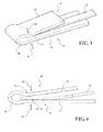
FIG. 3 is an enlarged schematic perspective view illustration of the first embodiment of the arrangement for securing the input circuit to the leadframe ofFigs. 1-2 ; -
FIG. 4 is an enlarged schematic side view illustration of the first embodiment of the arrangement for securing the input circuit to the leadframe ofFigs. 1-3 ; -
FIG. 5 is a schematic side view illustration of a second embodiment of the present invention; -
FIG. 6 is a schematic side view illustration of a third embodiment of the present invention; -
FIG. 7 is a schematic side view illustration of a fourth embodiment of the present invention; and -
FIG. 8 is a schematic side view illustration of a fifth embodiment of the present invention. - The following description is merely exemplary in nature and is in no way intended to limit the disclosure, its application, or uses. For purposes of clarity, the same reference numbers will be used in the drawings to identify similar elements.
Figures 1-2 illustrate anautomotive component assembly 10. Theautomotive component assembly 10 includes aninput circuit portion 12 and acomponent portion 14. Theinput circuit portion 12 may be an input circuit for any type of sensor, such as an engine speed sensor. Thecomponent portion 14 may be any type of component which theinput circuit portion 12 needs to be secured, such as a leadframe. - The
input circuit portion 12 has a first terminal 16 and a second terminal 18 (not numbered), which must both be in electrical contact with thecomponent portion 14 once assembled. Theinput circuit portion 12 portion is position along thecomponent portion 14 in a desired assembly position. For example, theinput circuit portion 12 is axially aligned along the leadframe. - The
input circuit portion 12 is assembled to thecomponent portion 14 by folding a portion of thecomponent portion 14 back over itself, such that theinput circuit portion 12 is positioned between afirst layer 20 and asecond layer 22 of thecomponent portion 14. Thefirst layer 20 and thesecond layer 22 define apocket 24, which theinput circuit portion 12 is located. - A
clamping force 26 is applied to press thefirst layer 20 and thesecond layer 22 toward one another. Theclamping force 26 applies enough pressure to theinput circuit portion 12 to ensure sufficient contact between the terminals 16, 18 and theleadframe 14, while being low enough to not damage theinput circuit portion 12. Theclamping force 26 may be applied by any technique which is capable of applying the force in a manner that desired for a particularinput circuit portion 12 andcomponent portion 14 design. - Additionally, the
component portion 14 may be shaped such that thepocket 24 is at least partially defined prior to theclamping force 26 being applied, with enough distance between thelayers input circuit portion 12 easy. In this manner, thefold 30 defining a portion of thepocket 24 can be used as a guide for positioning theinput circuit portion 12 relative to thecomponent portion 14. The radius of thefold 30 may be optimized, for the desired shape ofpocket 24 and contact between thelayers input circuit portion 12, especially the terminals 16, 18. Additionally contact points 32 (not shown) may be formed on thefirst layer 20 and/orsecond layer 22 designed to align with the terminals 16, 18 and provide the most favorable surface area and pressure of the contact between thecomponent portion 14 and the terminals 16, 18. - Once the
clamping force 26 has been applied, an overmold material 28 (not shown) is applied to theassembly 10 to secure theinput circuit portion 12 andcomponent portion 14 together. The overmoldmaterial 28 increases the resistance to vibration, thermo-mechanical stress, and other environmental stresses of theassembly 10. - The pressing operation for assembling the
sensor portion 12 to thecomponent portion 14 is faster and uses less material than the welding or soldering process of securing thesensor portion 12 to theleadframe 14. -
Figure 5 illustrates a second embodiment of anassembly 110 having thesensor portion 112 and thecomponent portion 114.First layer 120 andsecond layer 122 are spaced part to receive thesensor portion 112. Thepocket 124 has a specified shape and diameter that is ideal for thatparticular assembly 110. Thesecond layer 122 is shaped to havemultiple contact points 121. Thesensor 112 should be positioned such that terminals 116, 118 substantially align with thecontact points 121.Force 26 is applied at thecontact points 121 such that thefirst layer 120,second layer 122 andsensor 112 have electrical contact with one another. -
Figure 6 illustrates a third embodiment of anassembly 210 having thesensor portion 212 and thecomponent portion 214.First layer 220 andsecond layer 222 are spaced part to receive thesensor portion 212. Thepocket 224 has a specified shape and diameter that is ideal for thatparticular assembly 210. Thesecond layer 222 has a shape the extends in a curved manner away from thefirst layer 220 to have a wide lead in opening for receiving thesensor portion 212. Thesensor 212 should be positioned such that terminals 216, 218 are substantially aligned with acontact point 221.Force 26 is applied at thecontact point 221 such that thefirst layer 220,second layer 222 andsensor 212 have electrical contact with one another. -
Figure 7 illustrates a fourth embodiment of anassembly 310 having thesensor portion 312 and thecomponent portion 314.First layer 320 andsecond layer 322 are spaced part to receive thesensor portion 312. Thepocket 324 has a specified shape and diameter that is ideal for thatparticular assembly 310. In this embodiment the pocket is small such thatcontact 321 between thesecond layer 322 and thesensor 312 occurs over a predefined area instead of at a single point. Thesecond layer 322 has a shape the extends in a curved manner away from thefirst layer 320 to have a lead in opening for receiving thesensor portion 312 to make assembly of the components easier. Thesensor 312 should be positioned such that terminals 316, 318 are substantially aligned with thecontact area 321.Force 26 is applied at thecontact area 321 in multiple locations, such that thefirst layer 320,second layer 322 andsensor 312 have electrical contact with one another. -
Figure 8 illustrates a fourth embodiment of anassembly 410 having thesensor portion 412 and thecomponent portion 414.First layer 420 andsecond layer 422 are spaced part to receive thesensor portion 412. Thepocket 424 has a specified shape and diameter that is ideal for thatparticular assembly 410. Thesecond layer 422 has a shape the extends in a curved manner away from thefirst layer 420 to have a lead in opening for receiving thesensor portion 412 to make assembly of the components easier. Thesensor 412 should be positioned such thatterminals Force 26 is applied at the contact points 421, such that thefirst layer 420,second layer 422 andsensor 412 have electrical contact with one another.Sufficient force 26 may be applied to deform thesecond layer 422 andsensors 412 to increase the contact betweensensor 412 and component portion and ensure sufficient electrical contact. - While the best modes for carrying out the invention have been described in detail the true scope of the disclosure should not be so limited, since those familiar with the art to which this invention relates will recognize various alternative designs and embodiments for practicing the invention within the scope of the appended claims.
Claims (16)
- A component assembly comprising:a input circuit portion for an electronic component;a component portion, wherein the input circuit portion is aligned with the component portion in a desired assembly position;a pocket at least partially defined by the component portion to receive the input circuit portion; andwherein a clamping force retains the input circuit portion between a first layer and a second layer of the component portion forming the pocket
- The component assembly of claim 1, wherein the component portion is a leadframe.
- The component assembly of claim 1 or 2, wherein the input circuit portion is an engine speed sensor.
- The component assembly of one of the claims 1 to 3, wherein contact points on at least one of the first layer and the second layer are aligned with first and second terminals on the input circuit portion.
- The component assembly of one of the claims 1 to 4, wherein a fold in the automotive component at least partially defines the pocket.
- The component assembly of one of the claims 1 to 5, wherein at least the first layer is deformed at the contact points by the clamping force to increase electrical contact between the input circuit portion and the component portion.
- The component assembly of one of the claims 1 to 6, wherein the second layer extends in a curved manner away from the first layer to received the input circuit portion therebetween.
- The component assembly of one of the claims 1 to 7, wherein an overmold material retains the input circuit portion and the component portion to one another
- A method of assembling an automotive component assembly comprising:aligning an input circuit portion with a component portion in a desired assembly position;applying a clamping force to press a first layer and an second layer of the component portion toward one another, such that the input circuit portion is secured between the first layer and the second layer; andapplying an overmold material to the assembled input circuit portion and the component portion to retain the input circuit portion and the component portion to one another.
- The method of claim 9, wherein the component portion is a leadframe.
- The method of claim 9 or 10, wherein the sensor portion is an engine speed sensors.
- The method of one of the claims 9 to 11, further comprising aligning contact points on at least one of the first layer and the second layer with respective first and second terminals on the input circuit portion.
- The method of claim 12, further comprising deforming at least the first layer with the clamping force at the contact points to increase electrical contact between the input circuit portion and the component portion.
- The method of one of the claims 9 to 13, wherein the first layer and the second layer of the component portion at least partially define a pocket, and aligning the input circuit portion in the desired assembly position further comprises aligning the input circuit portion with the pocket.
- The method of claim 14, further comprising using a fold that at least partially defines the pocket as a guide to align the input circuit portion.
- The method of one of the claims 9 to 15, wherein the second layer extends in a curved manner away from the first layer to received the input circuit portion therebetween.
Applications Claiming Priority (2)
| Application Number | Priority Date | Filing Date | Title |
|---|---|---|---|
| US201462061857P | 2014-10-09 | 2014-10-09 | |
| US14/878,644 US10539585B2 (en) | 2014-10-09 | 2015-10-08 | Arrangement and method for connecting an electrical component to a leadframe |
Publications (1)
| Publication Number | Publication Date |
|---|---|
| EP3007527A1 true EP3007527A1 (en) | 2016-04-13 |
Family
ID=54329386
Family Applications (1)
| Application Number | Title | Priority Date | Filing Date |
|---|---|---|---|
| EP15189149.6A Withdrawn EP3007527A1 (en) | 2014-10-09 | 2015-10-09 | Arrangement and method for connecting an electrical component to a circuit portion |
Country Status (2)
| Country | Link |
|---|---|
| US (1) | US10539585B2 (en) |
| EP (1) | EP3007527A1 (en) |
Cited By (1)
| Publication number | Priority date | Publication date | Assignee | Title |
|---|---|---|---|---|
| DE102017214780A1 (en) * | 2017-08-23 | 2019-02-28 | Conti Temic Microelectronic Gmbh | Sensor component, pre-assembly arrangement for a sensor component and method for producing a sensor component |
Citations (8)
| Publication number | Priority date | Publication date | Assignee | Title |
|---|---|---|---|---|
| GB1518397A (en) * | 1976-10-23 | 1978-07-19 | Amp Inc | Light emitting diode mounting |
| JPS61123818A (en) * | 1984-11-21 | 1986-06-11 | Hitachi Ltd | liquid crystal display element |
| US4870224A (en) * | 1988-07-01 | 1989-09-26 | Intel Corporation | Integrated circuit package for surface mount technology |
| US5847934A (en) * | 1996-05-20 | 1998-12-08 | Mitsubishi Denki Kabushiki Kaisha | Hybrid integrated circuit |
| EP0970594A1 (en) * | 1997-03-27 | 2000-01-12 | Ford Motor Company | Moulded sockets for electronic component attachment |
| US20020159238A1 (en) * | 2001-04-27 | 2002-10-31 | Kurt Gross | Mounting configuration of electric and/or electronic components on a printed circuit board |
| DE102006046594A1 (en) * | 2005-10-18 | 2007-04-19 | Marquardt Gmbh | Electrical switching arrangement used in electrical household appliances or in electric tools comprises a substrate with a metal part having spring clips arranged so that the substrate is held on the metal part |
| WO2011113863A1 (en) * | 2010-03-17 | 2011-09-22 | Robert Bosch Gmbh | Arrangement comprising an electric and/or electronic module and a circuit carrier |
Family Cites Families (7)
| Publication number | Priority date | Publication date | Assignee | Title |
|---|---|---|---|---|
| DE2841553C2 (en) * | 1978-09-23 | 1982-08-26 | Robert Bosch Gmbh, 7000 Stuttgart | Flexural oscillator knock sensor |
| US5233131A (en) * | 1990-12-19 | 1993-08-03 | Vlsi Technology, Inc. | Integrated circuit die-to-leadframe interconnect assembly system |
| US5525956A (en) * | 1993-03-30 | 1996-06-11 | Hokuriku Electric Industry Co., Ltd. | Electrical terminal construction for an electronic component |
| US5743751A (en) * | 1996-05-14 | 1998-04-28 | Davis; Philip E. | Straddle adapter for mounting edge connectors to a printed circuit board |
| US5898321A (en) | 1997-03-24 | 1999-04-27 | Intel Corporation | Method and apparatus for slew rate and impedance compensating buffer circuits |
| US7863527B2 (en) * | 2007-02-23 | 2011-01-04 | Continental Automotive Systems Us, Inc. | Lead frame mount for circuit component |
| EP2392920B1 (en) * | 2009-12-25 | 2015-02-11 | NGK Insulators, Ltd. | Connector |
-
2015
- 2015-10-08 US US14/878,644 patent/US10539585B2/en active Active
- 2015-10-09 EP EP15189149.6A patent/EP3007527A1/en not_active Withdrawn
Patent Citations (8)
| Publication number | Priority date | Publication date | Assignee | Title |
|---|---|---|---|---|
| GB1518397A (en) * | 1976-10-23 | 1978-07-19 | Amp Inc | Light emitting diode mounting |
| JPS61123818A (en) * | 1984-11-21 | 1986-06-11 | Hitachi Ltd | liquid crystal display element |
| US4870224A (en) * | 1988-07-01 | 1989-09-26 | Intel Corporation | Integrated circuit package for surface mount technology |
| US5847934A (en) * | 1996-05-20 | 1998-12-08 | Mitsubishi Denki Kabushiki Kaisha | Hybrid integrated circuit |
| EP0970594A1 (en) * | 1997-03-27 | 2000-01-12 | Ford Motor Company | Moulded sockets for electronic component attachment |
| US20020159238A1 (en) * | 2001-04-27 | 2002-10-31 | Kurt Gross | Mounting configuration of electric and/or electronic components on a printed circuit board |
| DE102006046594A1 (en) * | 2005-10-18 | 2007-04-19 | Marquardt Gmbh | Electrical switching arrangement used in electrical household appliances or in electric tools comprises a substrate with a metal part having spring clips arranged so that the substrate is held on the metal part |
| WO2011113863A1 (en) * | 2010-03-17 | 2011-09-22 | Robert Bosch Gmbh | Arrangement comprising an electric and/or electronic module and a circuit carrier |
Cited By (2)
| Publication number | Priority date | Publication date | Assignee | Title |
|---|---|---|---|---|
| DE102017214780A1 (en) * | 2017-08-23 | 2019-02-28 | Conti Temic Microelectronic Gmbh | Sensor component, pre-assembly arrangement for a sensor component and method for producing a sensor component |
| US11536594B2 (en) | 2017-08-23 | 2022-12-27 | Vitesco Technologies Germany Gmbh | Sensor component, pre-assembly arrangement for a sensor component, and method for producing a sensor component |
Also Published As
| Publication number | Publication date |
|---|---|
| US20160103147A1 (en) | 2016-04-14 |
| US10539585B2 (en) | 2020-01-21 |
Similar Documents
| Publication | Publication Date | Title |
|---|---|---|
| US9093780B2 (en) | Press-fit pin, connection structure including the press-fit pin, and electronic device including the press-fit pin | |
| EP2167930B1 (en) | Connection unit for a pressure measuring cell | |
| KR20130135913A (en) | Fixed structure of separate leaf springs | |
| US9698506B2 (en) | Electric connection structure | |
| EP3185267A1 (en) | Capacitor and manufacturing method therefor | |
| US9791338B2 (en) | Pressure sensor capable of improving assembling efficiency by using spring electrode | |
| EP3185364A1 (en) | Press-fit terminal | |
| EP3576118A1 (en) | Capacitor and method for manufacturing same | |
| WO2015121486A1 (en) | Preassembled assembly for a sensor unit, and corresponding sensor unit | |
| US20120161362A1 (en) | Method for Producing an Electronic Component | |
| CN106879162A (en) | Flexible printed circuit board and the lamp module for motor vehicles including the printed circuit board (PCB) | |
| DE102014216158A1 (en) | Connection device for a pressure sensor, pressure sensor and method for producing a connection device | |
| US10539585B2 (en) | Arrangement and method for connecting an electrical component to a leadframe | |
| TW201611691A (en) | Method for press-free electrical contact of a conductive press-in pin in a circuit board without soldering | |
| US9030840B2 (en) | Arrangement comprising an electric and/or electronic module and a circuit carrier | |
| US9707924B2 (en) | Method for mounting a gas generator, and subassembly comprising a gas generator | |
| TWI693620B (en) | Lead terminal for electrolytic capacitor, electrolytic capacitor and manufacturing method of electrolytic capacitor | |
| DE102013202898B4 (en) | Sensor component for a pressure sensor | |
| EP3007524A2 (en) | Arrangement and method for connecting electronic components to a terminal for a sensor assembly | |
| US7863527B2 (en) | Lead frame mount for circuit component | |
| JP6307365B2 (en) | Terminal, terminal mounting structure, and electrical junction box comprising said terminal | |
| CN106102957A (en) | Method for establishing component connection system and component connection system | |
| JP6292111B2 (en) | Press-fit terminal | |
| US20170097029A1 (en) | Method for Connecting a Ball to a First Component in a Positively Locking Manner, and Component Connection | |
| EP3308873B1 (en) | Method of manufacturing a washer |
Legal Events
| Date | Code | Title | Description |
|---|---|---|---|
| PUAI | Public reference made under article 153(3) epc to a published international application that has entered the european phase |
Free format text: ORIGINAL CODE: 0009012 |
|
| AK | Designated contracting states |
Kind code of ref document: A1 Designated state(s): AL AT BE BG CH CY CZ DE DK EE ES FI FR GB GR HR HU IE IS IT LI LT LU LV MC MK MT NL NO PL PT RO RS SE SI SK SM TR |
|
| AX | Request for extension of the european patent |
Extension state: BA ME |
|
| STAA | Information on the status of an ep patent application or granted ep patent |
Free format text: STATUS: THE APPLICATION HAS BEEN PUBLISHED |
|
| STAA | Information on the status of an ep patent application or granted ep patent |
Free format text: STATUS: THE APPLICATION IS DEEMED TO BE WITHDRAWN |
|
| 18D | Application deemed to be withdrawn |
Effective date: 20161014 |