EP3007357A1 - Surface acoustic wave device - Google Patents
Surface acoustic wave device Download PDFInfo
- Publication number
- EP3007357A1 EP3007357A1 EP14804827.5A EP14804827A EP3007357A1 EP 3007357 A1 EP3007357 A1 EP 3007357A1 EP 14804827 A EP14804827 A EP 14804827A EP 3007357 A1 EP3007357 A1 EP 3007357A1
- Authority
- EP
- European Patent Office
- Prior art keywords
- acoustic wave
- surface acoustic
- piezoelectric substrate
- resin
- wave device
- Prior art date
- Legal status (The legal status is an assumption and is not a legal conclusion. Google has not performed a legal analysis and makes no representation as to the accuracy of the status listed.)
- Granted
Links
Images





Classifications
-
- H—ELECTRICITY
- H03—ELECTRONIC CIRCUITRY
- H03H—IMPEDANCE NETWORKS, e.g. RESONANT CIRCUITS; RESONATORS
- H03H9/00—Networks comprising electromechanical or electro-acoustic elements; Electromechanical resonators
- H03H9/25—Constructional features of resonators using surface acoustic waves
-
- H—ELECTRICITY
- H03—ELECTRONIC CIRCUITRY
- H03H—IMPEDANCE NETWORKS, e.g. RESONANT CIRCUITS; RESONATORS
- H03H9/00—Networks comprising electromechanical or electro-acoustic elements; Electromechanical resonators
- H03H9/02—Details
- H03H9/02535—Details of surface acoustic wave devices
- H03H9/02818—Means for compensation or elimination of undesirable effects
- H03H9/02897—Means for compensation or elimination of undesirable effects of strain or mechanical damage, e.g. strain due to bending influence
-
- H—ELECTRICITY
- H03—ELECTRONIC CIRCUITRY
- H03H—IMPEDANCE NETWORKS, e.g. RESONANT CIRCUITS; RESONATORS
- H03H9/00—Networks comprising electromechanical or electro-acoustic elements; Electromechanical resonators
- H03H9/02—Details
- H03H9/02535—Details of surface acoustic wave devices
- H03H9/02543—Characteristics of substrate, e.g. cutting angles
- H03H9/02574—Characteristics of substrate, e.g. cutting angles of combined substrates, multilayered substrates, piezoelectrical layers on not-piezoelectrical substrate
-
- H—ELECTRICITY
- H03—ELECTRONIC CIRCUITRY
- H03H—IMPEDANCE NETWORKS, e.g. RESONANT CIRCUITS; RESONATORS
- H03H9/00—Networks comprising electromechanical or electro-acoustic elements; Electromechanical resonators
- H03H9/02—Details
- H03H9/02535—Details of surface acoustic wave devices
- H03H9/02818—Means for compensation or elimination of undesirable effects
- H03H9/02834—Means for compensation or elimination of undesirable effects of temperature influence
-
- H—ELECTRICITY
- H03—ELECTRONIC CIRCUITRY
- H03H—IMPEDANCE NETWORKS, e.g. RESONANT CIRCUITS; RESONATORS
- H03H9/00—Networks comprising electromechanical or electro-acoustic elements; Electromechanical resonators
- H03H9/02—Details
- H03H9/02535—Details of surface acoustic wave devices
- H03H9/02992—Details of bus bars, contact pads or other electrical connections for finger electrodes
-
- H—ELECTRICITY
- H03—ELECTRONIC CIRCUITRY
- H03H—IMPEDANCE NETWORKS, e.g. RESONANT CIRCUITS; RESONATORS
- H03H9/00—Networks comprising electromechanical or electro-acoustic elements; Electromechanical resonators
- H03H9/02—Details
- H03H9/05—Holders or supports
- H03H9/10—Mounting in enclosures
- H03H9/1064—Mounting in enclosures for surface acoustic wave [SAW] devices
- H03H9/1071—Mounting in enclosures for surface acoustic wave [SAW] devices the enclosure being defined by a frame built on a substrate and a cap, the frame having no mechanical contact with the SAW device
-
- H—ELECTRICITY
- H03—ELECTRONIC CIRCUITRY
- H03H—IMPEDANCE NETWORKS, e.g. RESONANT CIRCUITS; RESONATORS
- H03H9/00—Networks comprising electromechanical or electro-acoustic elements; Electromechanical resonators
- H03H9/02—Details
- H03H9/02535—Details of surface acoustic wave devices
- H03H9/02543—Characteristics of substrate, e.g. cutting angles
- H03H9/02559—Characteristics of substrate, e.g. cutting angles of lithium niobate or lithium-tantalate substrates
-
- H—ELECTRICITY
- H03—ELECTRONIC CIRCUITRY
- H03H—IMPEDANCE NETWORKS, e.g. RESONANT CIRCUITS; RESONATORS
- H03H9/00—Networks comprising electromechanical or electro-acoustic elements; Electromechanical resonators
- H03H9/02—Details
- H03H9/02535—Details of surface acoustic wave devices
- H03H9/02818—Means for compensation or elimination of undesirable effects
- H03H9/02929—Means for compensation or elimination of undesirable effects of ageing changes of characteristics, e.g. electro-acousto-migration
-
- H—ELECTRICITY
- H03—ELECTRONIC CIRCUITRY
- H03H—IMPEDANCE NETWORKS, e.g. RESONANT CIRCUITS; RESONATORS
- H03H9/00—Networks comprising electromechanical or electro-acoustic elements; Electromechanical resonators
- H03H9/02—Details
- H03H9/05—Holders or supports
- H03H9/10—Mounting in enclosures
- H03H9/1007—Mounting in enclosures for bulk acoustic wave [BAW] devices
- H03H9/1042—Mounting in enclosures for bulk acoustic wave [BAW] devices the enclosure being defined by a housing formed by a cavity in a resin
-
- H—ELECTRICITY
- H03—ELECTRONIC CIRCUITRY
- H03H—IMPEDANCE NETWORKS, e.g. RESONANT CIRCUITS; RESONATORS
- H03H9/00—Networks comprising electromechanical or electro-acoustic elements; Electromechanical resonators
- H03H9/02—Details
- H03H9/125—Driving means, e.g. electrodes, coils
- H03H9/145—Driving means, e.g. electrodes, coils for networks using surface acoustic waves
- H03H9/14538—Formation
- H03H9/14541—Multilayer finger or busbar electrode
Definitions
- the present invention relates to a surface acoustic wave device that includes a surface acoustic wave element such as a SAW (Surface Acoustic Wave) filter or a SAW resonator, and that has a package structure surrounding the surface acoustic wave element.
- a surface acoustic wave element such as a SAW (Surface Acoustic Wave) filter or a SAW resonator
- Patent Document 1 Japanese Unexamined Patent Application Publication No. 11-88101 describes a surface acoustic wave element 102 illustrated in Fig. 8 .
- the surface acoustic wave element 102 includes a piezoelectric substrate 111, a dielectric film 112 disposed on the piezoelectric substrate 111, and IDT (Inter Digital Transducer) electrodes 113 and 114 both disposed on the dielectric film 112.
- IDT Inter Digital Transducer
- the dielectric film 112 is a film for adjusting a fractional bandwidth of the surface acoustic wave element 102.
- a material of the dielectric film 112 is a metal oxide. For example, SiO 2 is used as the material. From the viewpoint of easiness in manufacturing, as illustrated in Fig. 8 , the dielectric film 112 is formed over the entirety of a principal surface 111M of the piezoelectric substrate 111 by, e.g., sputtering.
- the surface acoustic wave element 102 further includes a characteristic compensating dielectric portion 121 that covers the IDT electrodes 113 and 114. The characteristic compensating dielectric portion 121 is to compensate for variations in frequency characteristics such that the frequency characteristics are not significantly changed even when the temperature of the surface acoustic wave element 102 is changed.
- Fig. 9 illustrates a surface acoustic wave device 101 including the surface acoustic wave element 102 and having a package structure.
- the surface acoustic wave device 101 includes, in addition to the surface acoustic wave element 102, a resin member 115 disposed on the piezoelectric substrate 111.
- the resin member 115 is constituted by a resin support portion 115A in the shape of a frame, and a resin cover portion 115B that is disposed in a state covering the IDT electrodes 113 and 114 in cooperation with the resin support portion 115A.
- the piezoelectric substrate 111 and the resin member 115 define a space S that is held in an airtight condition to allow excitation of a surface acoustic wave in the space.
- the surface acoustic wave device 101 further includes via conductors 118 through which signals are supplied to the surface acoustic wave element 102.
- Patent Document 1 Japanese Unexamined Patent Application Publication No. 11-88101
- the piezoelectric substrate 111 is made of an inorganic piezoelectric material such as lithium niobate, and the resin member 115 is made of resin. Because the piezoelectric substrate 111 and the resin member 115 are made of different materials, their linear expansion coefficients are different from each. Therefore, when the surface acoustic wave device 101 is placed in an environment subjected to temperature variations, thermal stress is generated with expansion or contraction of the piezoelectric substrate 111 and the resin member 115.
- the resin support portion 115A and the resin cover portion 115B of the resin member 115 are both made of resin materials and respective values of the linear expansion coefficients of the resin materials are close to each other, influences of the thermal stress on both the portions are small. Accordingly, peeling-off is hard to occur between the resin support portion 115A and the resin cover portion 115B.
- the linear expansion coefficients of the piezoelectric substrate 111 and the resin support portion 115A are different from each other, a shearing force is generated in a direction parallel to the interface between the piezoelectric substrate 111 and the resin support portion 115A upon the generation of the thermal stress.
- the dielectric film 112 is disposed between the principal surface 111M of the piezoelectric substrate 111 and the resin support portion 115A.
- An adhesion force of the dielectric film 112 with respect to the piezoelectric substrate 111 is weak. Accordingly, if the above-mentioned shearing force is generated, peeling-off is likely to occur between the piezoelectric substrate 111 and the dielectric film 112. This results in a problem that, in the package structure of the surface acoustic wave device 101, it is difficult to maintain the interior in the airtight condition.
- An object of the present invention is to provide a surface acoustic wave device that can suppress peeling-off between a piezoelectric substrate and a resin member and can maintain the interior in an airtight condition even when thermal stress is generated between the piezoelectric substrate and the resin member in an atmosphere subjected to temperature variations.
- the present invention provides a surface acoustic wave device including a piezoelectric substrate, a dielectric film disposed on a principal surface of the piezoelectric substrate, IDT electrodes disposed on the piezoelectric substrate with the dielectric film interposed therebetween, and a resin member disposed on the piezoelectric substrate in a state spaced from the IDT electrodes and covering the IDT electrodes, wherein the surface acoustic wave device includes a resin contact region where the piezoelectric substrate and the resin member are in direct contact with each other, and the resin contact region has a shape surrounding the IDT electrodes.
- the surface acoustic wave device further includes junction electrodes disposed on the principal surface of the piezoelectric substrate for electrical connection to the IDT electrodes, and via conductors disposed at least in the resin member for electrical connection to the junction electrodes, wherein, when looking at, in a projection view, the surface acoustic wave device from the side facing the principal surface of the piezoelectric substrate, the via conductors are present at positions overlapping the junction electrodes, but not overlapping the dielectric film.
- the resin member includes a resin support portion disposed in a state surrounding the IDT electrodes, and a resin cover portion disposed on the resin support portion in a state spaced from the IDT electrodes and covering the IDT electrodes, wherein, when looking at, in a projection view, the surface acoustic wave device from the side facing the principal surface of the piezoelectric substrate, the resin support portion is present at a position not overlapping the dielectric film.
- the resin contact region has a shape of a closed frame.
- the surface acoustic wave device includes the resin contact region where the piezoelectric substrate and the resin member are in direct contact with each other. Furthermore, the resin contact region has the shape surrounding the IDT electrodes. Since the resin member exhibits a stronger adhesion force with respect to the piezoelectric substrate than the dielectric film, the adhesion force of the resin member with respect to the piezoelectric substrate can be increased in the surface acoustic wave device according to the present invention than in the case of the dielectric film being interposed therebetween, i.e., in the surface acoustic wave device disclosed in the above description of "Background Art". Thus, even when the surface acoustic wave device is placed in an environment subjected to temperature variations, peeling-off between the piezoelectric substrate and the resin member can be suppressed, and the interior can be maintained in an airtight condition.
- a surface acoustic wave device 1 includes a piezoelectric substrate 11, a dielectric film 12, IDT (Inter Digital Transducer) electrodes 13 and 14, and a resin member 15.
- a surface acoustic wave element is constituted by the piezoelectric substrate 11, the dielectric film, and the IDT electrodes 13 and 14.
- the resin member 15 is constituted by a resin support portion 15A and a resin cover portion 15B.
- the resin support portion 15A and the resin cover portion 15B may be formed in an integral unit by employing the same material.
- the surface acoustic wave device 1 may further include junction electrodes 17 and via conductors 18.
- the surface acoustic wave device 1 has a package structure in which the piezoelectric substrate 11 and the resin member 15 define an outer periphery. With the package structure, an inner space S is sealed and held in an airtight condition. As described above, in an environment subjected to temperature variations, thermal stress is generated in the surface acoustic wave device 1 between the piezoelectric substrate 11 and the resin member 15.
- the surface acoustic wave device 1 according to the embodiment has a structure such that the piezoelectric substrate 11 and the resin member 15 are hard to peel off even when the thermal stress is generated.
- temperature variations used herein implies, for example, temperature variations in a heat cycle test that is defined in JEDJESD 22-Al04C specified by JEDEC (Solid State Technology Association).
- the structure of the surface acoustic wave device 1 will be described below with reference to Figs. 1 , 2(A) and 2(B) .
- the piezoelectric substrate 11 is a base member of the surface acoustic wave device 1.
- the piezoelectric substrate 11 is made of an inorganic piezoelectric material that is, e.g., lithium niobate, potassium niobate, lithium tantalate, quartz, langasite, zinc oxide, lead zirconate titanate, or lithium tetraborate.
- a 127° rotated Y cut X SAW propagation LiNbO 3 is used in the embodiment.
- the dielectric film 12 is disposed on a principal surface 11M of the piezoelectric substrate 11, and it has a predetermined pattern.
- the dielectric film 12 is a film for adjusting a fractional bandwidth of the surface acoustic wave device 1.
- the dielectric film 12 is disposed at least between the principal surface 11M of the piezoelectric substrate 11 and the IDT electrodes 13 and 14 (see a left half of the sectional view illustrated in Fig. 2(B) ).
- a pattern of the dielectric film 12 is not always required to be the same as patterns of the IDT electrodes 13 and 14, and that the dielectric film 12 may be disposed on the principal surface 11M of the piezoelectric substrate 11 in a larger area than the patterns of the IDT electrodes 13 and 14 (see a right half of the sectional view illustrated in Fig. 2(B) ).
- the dielectric film 12 is first formed over the entirety of the principal surface 11M of the piezoelectric substrate 11 by an ordinary film-forming process, e.g., a sputtering or CVD.
- the dielectric film 12 is then formed into a predetermined pattern through the steps of patterning a photoresist, and removing parts of the dielectric film 12 having been formed over the entire principal surface 11M, by a proper etching process, such as dry etching or wet etching.
- a proper etching process such as dry etching or wet etching.
- a material of the dielectric film 12 is a metal oxide or a metal nitride.
- SiO 2 , Si 3 N 4 , SiON, SiO, Ta 2 O 5 , TiO 2 , TiN, AIN, Al 2 O 3 , or TeO 2 is used.
- the IDT electrodes 13 and 14 are disposed on the piezoelectric substrate 11 with the dielectric film 12 disposed therebetween.
- the IDT electrodes 13 and 14 include respectively pluralities of electrode fingers 13A and 14A arrayed in the propagation direction (X-direction) of a surface acoustic wave, bus bars 13B and 14B connected respectively to the pluralities of electrode fingers 13A and 14A, and lead-out portions 13C and 14C connected respectively to the bus bars 13B and 14B.
- the electrode fingers 13A and 14A are alternately arrayed in the propagation direction of the surface acoustic wave.
- the IDT electrodes 13 and 14 are each made of a multilayer film that is formed by laminating a NiCr layer, a Pt layer, a Ti layer, an AlCu layer, and a Ti layer in the mentioned order.
- the IDT electrodes 13 and 14 are each formed by patterning the multilayer film, which has been obtained with a thin film-forming method, through a lift-off process.
- Each of the IDT electrodes 13 and 14 has a thickness of 0.2 ⁇ m, for example.
- the IDT electrodes 13 and 14 are each formed to provide a wavelength of, e.g., 1.9 ⁇ m, and to have a metallization ratio of, e.g., 0.5.
- a pair of reflectors may be formed on both sides of the IDT electrodes 13 and 14 in the propagation direction of the surface acoustic wave.
- the resin support portion 15A of the resin member 15 is disposed at the outer peripheral side of the principal surface 11M of the piezoelectric substrate 11.
- the resin support portion 15A has the shape of a closed frame and is formed in a state continuously surrounding the IDT electrodes 13 and 14.
- a thickness of the resin support portion 15A is larger than a total value of the thickness of the dielectric film 12 and the thickness of each of the IDT electrodes 13 and 14.
- a material of the resin support portion 15A is, for example, a polyimide-based resin, an epoxy-based resin, an acrylic resin, a silicon-based resin, or a benzocyclobutene resin.
- the resin cover portion 15B of the resin member 15 is disposed on the resin support portion 15A such that the resin cover portion 15B is spaced from the IDT electrodes 13 and 14 by a certain distance and it covers the IDT electrodes 13 and 14. More specifically, the resin cover portion 15B is in the form of a film and is arranged parallel to the principal surface 11M of the piezoelectric substrate 11 in contact with the resin support portion 15A. With such an arrangement, the space S enclosed by the piezoelectric substrate 11 and the resin member 15 is formed in the surface acoustic wave device 1, thus allowing excitation of the surface acoustic wave in the space.
- a material of the resin cover portion 15B is, for example, a polyimide-based resin, an epoxy-based resin, an acrylic resin, a silicon-based resin, or a benzocyclobutene resin.
- Fig. 3 is a projection view when looking at, in a projection view, the surface acoustic wave device 1 from the side facing the principal surface 11M of the piezoelectric substrate 11.
- the surface acoustic wave device 1 includes a resin contact region RC where the piezoelectric substrate 11 and the resin member 15 are in direct contact with each other.
- a region hatched by oblique lines represents the resin contact region RC.
- the embodiment utilizes such a property that the resin material contained in the resin member 15 exhibits an adhesion force with respect to the piezoelectric substrate 11 stronger than that exhibited by the oxide material or the nitride material contained in the dielectric film 12.
- the piezoelectric substrate 11 and the resin member 15 are hard to peel off even when a shearing force acts between the piezoelectric substrate 11 and the resin member 15.
- the resin contact region RC has the shape of a closed frame surrounding the IDT electrodes 13 and 14. Therefore, a fluid (gas or liquid) is prevented from coming into or going out through a boundary between the piezoelectric substrate 11 and the resin member 15, and the airtight condition in the interior of the package structure can be maintained.
- the resin support portion 15A and the resin cover portion 15B are both made of the resin materials and respective values of the liner expansion coefficients of the resin materials are close to each other, an adhesion force between both the portions is strong. Accordingly, peeling-off between the resin support portion 15A and the resin cover portion 15B is hard to occur.
- the junction electrodes 17 are disposed on the principal surface 11M of the piezoelectric substrate 11 for electrical connection between the IDT electrodes 13 and 14 and the via conductors 18.
- the junction electrodes 17 are each a multilayer film that is formed by laminating an AlCu layer and a Ti layer, for example.
- the junction electrodes 17 are also formed by patterning the multilayer film, which has been obtained with a thin film-forming method, through a lift-off process.
- the junction electrodes 17 are each formed in a larger thickness than each of the IDT electrodes 13 and 14. In practice, the thickness of the junction electrode 17 is 2.5 ⁇ m, for example.
- the via conductors 18 are each formed in a state penetrating through the resin member 15 in a thickness direction thereof. Respective one ends of the via conductors 18 are electrically connected to corresponding ones of the IDT electrodes 13 and 14 through the junction electrodes 17. Respective other ends of the via conductors 18 are exposed to an outer surface of the resin cover portion 15B and are connected to external terminals 19.
- the via conductors 18 are each made of at least one general metal, such as Al, Pt, Cu, Au, Ti, Ni, Cr, W, Ag, Pd, Co or Mn.
- the via conductor 18 is formed, for example, as a multilayer film of Ni and Au by an electrolytic plating method.
- the via conductor 18 may be formed by fully filling a via hole with a conductor, or may have a hollow structure in which the via hole is partly filled with a conductor while a vacancy is left in its part.
- Fig. 3 regions denoted by cross hatching with lines extending in the X-direction and the Y-direction represent projection views VP of the via conductors 18. Regions denoted by cross hatching with lines extending at an angle of 45° relative to the X-direction and the Y-direction represent a projection view DP of the dielectric film 12. Regions surrounded by thick solid lines represent projection views EP of the junction electrodes 17. As illustrated in Fig.
- the via conductors 18 are disposed at positions overlapping the junction electrodes 17, but not overlapping the dielectric film 12.
- the via conductors 18 containing metals are each expanded or contracted in an axial direction (Z-direction), whereupon thermal stress is generated parallel to the axial direction of the via conductor 18.
- the dielectric film 112 is present between the piezoelectric substrate 111 and the resin support portion 115A as illustrated in Fig. 9 in the above description of "Background Art"
- the adhesion force of the dielectric film 112 with respect to the piezoelectric substrate 111 is weak, thus resulting in a possibility that the piezoelectric substrate 111 and the resin support portion 115A may be peeled off due to the thermal stress generated in the axial direction.
- the dielectric film 12 is not present in the axial direction of the via conductor 18, and the junction electrode 17 is present in that direction. Furthermore, the junction electrode 17 is in direct contact with the piezoelectric substrate 11 and is firmly held in a close contact state. Accordingly, even when the thermal stress is generated parallel to the axial direction of the via conductor 18, the piezoelectric substrate 11 and the junction electrode 17 are hard to peel off, and the piezoelectric substrate 11 and the resin support portion 15A are also hard to peel off. As a result, the airtight condition in the interior of the surface acoustic wave device 1 can be maintained. Moreover, since the adhesion force in the axial direction of the via conductor 18 is strong, breaks can be suppressed in the interconnections through the via conductors 18, the junction electrodes 17, and the IDT electrodes 13 and 14.
- a characteristic compensating dielectric portion 21 may be disposed in a state covering the IDT electrodes 13 and 14.
- the characteristic compensating dielectric portion 21 has such a compensation function that frequency characteristics are not significantly changed even when the temperature of the surface acoustic wave device 1 is changed.
- the characteristic compensating dielectric portion 21 is formed by a bias sputtering method, for example, and it has a thickness of 0.7 ⁇ m, for example.
- a material of the characteristic compensating dielectric portion 21 is preferably the same as that of the dielectric film 12.
- patterning of the characteristic compensating dielectric portion 21 and the dielectric film 12 can be performed by forming a resist on the characteristic compensating dielectric portion 21, and by etching the characteristic compensating dielectric portion 21 and the dielectric film 12 at the same time.
- the surface acoustic wave device 1 includes the resin contact region RC where the piezoelectric substrate 11 and the resin member 15 are in direct contact with each other. Furthermore, the resin contact region RC has the shape of a closed frame surrounding the IDT electrodes 13 and 14. Since the resin member 15 exhibits a stronger adhesion force with respect to the piezoelectric substrate 11 than the dielectric film 12, the adhesion force of the resin member 15 with respect to the piezoelectric substrate 11 can be increased in the surface acoustic wave device 1 according to the embodiment than in the case of the dielectric film 12 being interposed therebetween, i.e., in the surface acoustic wave device 101 disclosed in the above description of "Background Art". Thus, even when the surface acoustic wave device 1 is placed in an environment subjected to temperature variations, the peeling-off between the piezoelectric substrate 11 and the resin member 15 can be suppressed.
- the via conductors 18 are present at positions overlapping the junction electrodes 17, but not overlapping the dielectric film 12.
- the junction electrodes 17 are preferably present in the axial direction of the via conductors 18 instead of the dielectric film 12.
- the resin support portion 15A when looking at, in a projection view, the surface acoustic wave device 1 from the side facing the principal surface 11M of the piezoelectric substrate 11, the resin support portion 15A is preferably present at a position not overlapping the dielectric film 12 for the following reason.
- the resin support portion 15A exhibits a stronger adhesion force with respect to the piezoelectric substrate 11 than the dielectric film 12. Accordingly, adhesion strength with respect to the piezoelectric substrate 11 is increased in the entirety of the device by increasing an area in which the piezoelectric substrate 11 and the resin support portion 15A are in direct contact with each other.
- Figs. 4(A) and 4(B) to 6(A) and 6(B) illustrate typical modifications. Those modifications will be described below. It is to be noted that components common to those of the surface acoustic wave device 1 illustrated in Figs. 2(A) and 2(B) are denoted by the same reference signs in Figs. 4(A) to 6(B) and description of those components is omitted here.
- a surface acoustic wave device 1A illustrated in Figs. 4(A) and 4(B) represents a first modification of the surface acoustic wave device 1.
- the junction electrodes 17 are omitted, and via conductors 38 are connected to IDT electrodes 33 and 34. With the junction electrodes 17 being omitted, the number of components can be reduced.
- the surface acoustic wave device 1A according to the first modification also includes a resin contact region RC where the piezoelectric substrate 11 and a resin member 35 are in direct contact with each other. Furthermore, the resin contact region RC has the shape of a closed frame surrounding the IDT electrodes 33 and 34. As a result, even when the surface acoustic wave device 1A is placed in an environment subjected to temperature variations, peeling-off between the piezoelectric substrate 11 and the resin member 35 can be suppressed.
- a surface acoustic wave device 1B illustrated in Figs. 5(A) and 5(B) represents a second modification of the surface acoustic wave device 1.
- a dielectric film 42 and IDT electrodes 43 and 44 are partly buried and sandwiched between the piezoelectric substrate 11 and a resin support portion 45A.
- the surface acoustic wave device 1B according to the second modification also includes a resin contact region RC where the piezoelectric substrate 11 and a resin member 45 are in direct contact with each other. Furthermore, the resin contact region RC has the shape of a closed frame surrounding the IDT electrodes 43 and 44. As a result, even when the surface acoustic wave device 1B is placed in an environment subjected to temperature variations, peeling-off between the piezoelectric substrate 11 and the resin member 45 can be suppressed.
- via conductors 48 are present at positions overlapping junction electrodes 47, but not overlapping the dielectric film 42.
- the piezoelectric substrate 11 and the junction electrodes 47 are hard to peel off, and the piezoelectric substrate 11 and the resin member 45 are also hard to peel off.
- a surface acoustic wave device 1C illustrated in Figs. 6(A) and 6(B) represents a third modification of the surface acoustic wave device 1.
- via conductors 58 are each formed in a stepped shape. More specifically, as illustrated in Fig. 6(B) , the via conductor 58 is formed such that one end of the via conductor 58 is connected to the junction electrode 17, an intermediate portion of the via conductor 58 extends in the X-direction along a surface of a resin support portion 55A, and the remaining portion of the via conductor 58 penetrates through a resin cover portion 55B.
- the surface acoustic wave device 1C according to the third modification also includes a resin contact region RC where the piezoelectric substrate 11 and a resin member 55 are in direct contact with each other. Furthermore, the resin contact region RC has the shape of a closed frame surrounding the IDT electrodes 13 and 14. As a result, even when the surface acoustic wave device 1C is placed in an environment subjected to temperature variations, peeling-off between the piezoelectric substrate 11 and the resin member 55 can be suppressed.
- the via conductors 58 are present at positions overlapping the junction electrodes 17, but not overlapping the dielectric film 12.
- the piezoelectric substrate 11 and the junction electrodes 17 are hard to peel off, and the piezoelectric substrate 11 and the resin member 55 are also hard to peel off.
- the resin support portion is constituted in the shape of a closed frame surrounding the IDT electrodes, the resin support portion is not always required to be closed.
- a junction electrode 67 may be formed to extend up to an end surface of the substrate, and a resin support portion 65A may be partly opened at an extended end of the junction electrode 67. Even with such a structure, airtightness can be held satisfactorily.
- the resin support portion and the resin cover portion may be disposed as an integral unit on the substrate instead of being separate members.
- the surface acoustic wave device may be fabricated through the steps of forming a plurality of surface acoustic wave devices on a parent substrate, and then dividing the parent substrate into individual pieces.
- 1, 1A, 1B, 1C surface acoustic wave devices
- 11 piezoelectric substrate
- 11M principal surface of piezoelectric substrate
- 12 dielectric film
- 13 IDT electrodes
- 13A, 14A electrode fingers
- 13B, 14B bus bars
- 13C, 14C lead-out portions
- 15A resin support portion
- 15B resin cover portion
- 17 junction electrode
- 18 via conductor
- 19 external terminal
- 21 characteristic compensating dielectric portion
- RC resin contact region
- EP projection view of junction electrode
- VP projection view of via conductor
- DP projection view of dielectric film
Landscapes
- Physics & Mathematics (AREA)
- Acoustics & Sound (AREA)
- Surface Acoustic Wave Elements And Circuit Networks Thereof (AREA)
Abstract
Description
- The present invention relates to a surface acoustic wave device that includes a surface acoustic wave element such as a SAW (Surface Acoustic Wave) filter or a SAW resonator, and that has a package structure surrounding the surface acoustic wave element.
- Patent Document 1 (Japanese Unexamined Patent Application Publication No.
11-88101 acoustic wave element 102 illustrated inFig. 8 . The surfaceacoustic wave element 102 includes apiezoelectric substrate 111, adielectric film 112 disposed on thepiezoelectric substrate 111, and IDT (Inter Digital Transducer)electrodes dielectric film 112. - The
dielectric film 112 is a film for adjusting a fractional bandwidth of the surfaceacoustic wave element 102. A material of thedielectric film 112 is a metal oxide. For example, SiO2 is used as the material. From the viewpoint of easiness in manufacturing, as illustrated inFig. 8 , thedielectric film 112 is formed over the entirety of aprincipal surface 111M of thepiezoelectric substrate 111 by, e.g., sputtering. The surfaceacoustic wave element 102 further includes a characteristic compensatingdielectric portion 121 that covers theIDT electrodes dielectric portion 121 is to compensate for variations in frequency characteristics such that the frequency characteristics are not significantly changed even when the temperature of the surfaceacoustic wave element 102 is changed. -
Fig. 9 illustrates a surfaceacoustic wave device 101 including the surfaceacoustic wave element 102 and having a package structure. The surfaceacoustic wave device 101 includes, in addition to the surfaceacoustic wave element 102, aresin member 115 disposed on thepiezoelectric substrate 111. Theresin member 115 is constituted by aresin support portion 115A in the shape of a frame, and aresin cover portion 115B that is disposed in a state covering theIDT electrodes resin support portion 115A. Thepiezoelectric substrate 111 and theresin member 115 define a space S that is held in an airtight condition to allow excitation of a surface acoustic wave in the space. The surfaceacoustic wave device 101 further includes viaconductors 118 through which signals are supplied to the surfaceacoustic wave element 102. - Patent Document 1: Japanese Unexamined Patent Application Publication No.
11-88101 - The
piezoelectric substrate 111 is made of an inorganic piezoelectric material such as lithium niobate, and theresin member 115 is made of resin. Because thepiezoelectric substrate 111 and theresin member 115 are made of different materials, their linear expansion coefficients are different from each. Therefore, when the surfaceacoustic wave device 101 is placed in an environment subjected to temperature variations, thermal stress is generated with expansion or contraction of thepiezoelectric substrate 111 and theresin member 115. - Because the
resin support portion 115A and theresin cover portion 115B of theresin member 115 are both made of resin materials and respective values of the linear expansion coefficients of the resin materials are close to each other, influences of the thermal stress on both the portions are small. Accordingly, peeling-off is hard to occur between theresin support portion 115A and theresin cover portion 115B. On the other hand, because the linear expansion coefficients of thepiezoelectric substrate 111 and theresin support portion 115A are different from each other, a shearing force is generated in a direction parallel to the interface between thepiezoelectric substrate 111 and theresin support portion 115A upon the generation of the thermal stress. - In the surface
acoustic wave device 101 illustrated inFig. 9 , thedielectric film 112 is disposed between theprincipal surface 111M of thepiezoelectric substrate 111 and theresin support portion 115A. An adhesion force of thedielectric film 112 with respect to thepiezoelectric substrate 111 is weak. Accordingly, if the above-mentioned shearing force is generated, peeling-off is likely to occur between thepiezoelectric substrate 111 and thedielectric film 112. This results in a problem that, in the package structure of the surfaceacoustic wave device 101, it is difficult to maintain the interior in the airtight condition. - An object of the present invention is to provide a surface acoustic wave device that can suppress peeling-off between a piezoelectric substrate and a resin member and can maintain the interior in an airtight condition even when thermal stress is generated between the piezoelectric substrate and the resin member in an atmosphere subjected to temperature variations.
- The present invention provides a surface acoustic wave device including a piezoelectric substrate, a dielectric film disposed on a principal surface of the piezoelectric substrate, IDT electrodes disposed on the piezoelectric substrate with the dielectric film interposed therebetween, and a resin member disposed on the piezoelectric substrate in a state spaced from the IDT electrodes and covering the IDT electrodes, wherein the surface acoustic wave device includes a resin contact region where the piezoelectric substrate and the resin member are in direct contact with each other, and the resin contact region has a shape surrounding the IDT electrodes.
- Preferably, the surface acoustic wave device further includes junction electrodes disposed on the principal surface of the piezoelectric substrate for electrical connection to the IDT electrodes, and via conductors disposed at least in the resin member for electrical connection to the junction electrodes, wherein, when looking at, in a projection view, the surface acoustic wave device from the side facing the principal surface of the piezoelectric substrate, the via conductors are present at positions overlapping the junction electrodes, but not overlapping the dielectric film.
- Preferably, the resin member includes a resin support portion disposed in a state surrounding the IDT electrodes, and a resin cover portion disposed on the resin support portion in a state spaced from the IDT electrodes and covering the IDT electrodes, wherein, when looking at, in a projection view, the surface acoustic wave device from the side facing the principal surface of the piezoelectric substrate, the resin support portion is present at a position not overlapping the dielectric film.
- Preferably, the resin contact region has a shape of a closed frame.
- The surface acoustic wave device according to the present invention includes the resin contact region where the piezoelectric substrate and the resin member are in direct contact with each other. Furthermore, the resin contact region has the shape surrounding the IDT electrodes. Since the resin member exhibits a stronger adhesion force with respect to the piezoelectric substrate than the dielectric film, the adhesion force of the resin member with respect to the piezoelectric substrate can be increased in the surface acoustic wave device according to the present invention than in the case of the dielectric film being interposed therebetween, i.e., in the surface acoustic wave device disclosed in the above description of "Background Art". Thus, even when the surface acoustic wave device is placed in an environment subjected to temperature variations, peeling-off between the piezoelectric substrate and the resin member can be suppressed, and the interior can be maintained in an airtight condition.
-
- [
Fig. 1] Fig. 1 is a perspective view of a surfaceacoustic wave device 1 according to an embodiment of the present invention. - [
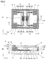
Fig. 2] Fig. 2(A) is a sectional view of the surfaceacoustic wave device 1 taken along Z1-Z1 denoted inFig. 2(B), and Fig. 2(B) is a sectional view of the surfaceacoustic wave device 1 taken along Y1-Y1 denoted inFig. 1 . - [
Fig. 3] Fig. 3 is a projection view when looking at, in a projection view, the surfaceacoustic wave device 1 from the side facing aprincipal surface 11M of apiezoelectric substrate 11. Regions surrounded by solid lines represent a resin contact region RC where thepiezoelectric substrate 11 and aresin member 15 are in contact with each other, projection views VP ofvia conductors 18, and a projection view DP of adielectric film 12. Regions surrounded by thick solid lines represent projection views EP ofjunction electrodes 17. Thin broken lines represent theIDT electrodes - [
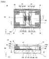
Fig. 4] Fig. 4 illustrates a first modification related to thedielectric film 12 and theIDT electrodes acoustic wave device 1. - [
Fig. 5] Fig. 5 illustrates a second modification related to thejunction electrodes 17 and thevia conductors 18 of the surfaceacoustic wave device 1. - [
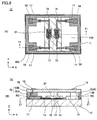
Fig. 6] Fig. 6 illustrates a third modification related to thevia conductors 18 of the surfaceacoustic wave device 1. - [
Fig. 7] Fig. 7 illustrates a fourth modification related to aresin support portion 15A of the surfaceacoustic wave device 1. - [
Fig. 8] Fig. 8 is a perspective view of a surfaceacoustic wave element 102 disclosed inPatent Document 1. - [
Fig. 9] Fig. 9 is a sectional view of a surfaceacoustic wave device 101 including the surfaceacoustic wave element 102, illustrated inFig. 8 , when looking from the front (Y-direction). - As illustrated in
Figs. 1 ,2(A) and 2(B) , a surfaceacoustic wave device 1 according to an embodiment includes apiezoelectric substrate 11, adielectric film 12, IDT (Inter Digital Transducer)electrodes resin member 15. A surface acoustic wave element is constituted by thepiezoelectric substrate 11, the dielectric film, and theIDT electrodes resin member 15 is constituted by aresin support portion 15A and aresin cover portion 15B. As theresin member 15, theresin support portion 15A and theresin cover portion 15B may be formed in an integral unit by employing the same material. The surfaceacoustic wave device 1 may further includejunction electrodes 17 and viaconductors 18. - The surface
acoustic wave device 1 has a package structure in which thepiezoelectric substrate 11 and theresin member 15 define an outer periphery. With the package structure, an inner space S is sealed and held in an airtight condition. As described above, in an environment subjected to temperature variations, thermal stress is generated in the surfaceacoustic wave device 1 between thepiezoelectric substrate 11 and theresin member 15. The surfaceacoustic wave device 1 according to the embodiment has a structure such that thepiezoelectric substrate 11 and theresin member 15 are hard to peel off even when the thermal stress is generated. - The term "temperature variations" used herein implies, for example, temperature variations in a heat cycle test that is defined in JEDJESD 22-Al04C specified by JEDEC (Solid State Technology Association).
- The structure of the surface
acoustic wave device 1 will be described below with reference toFigs. 1 ,2(A) and 2(B) . - The
piezoelectric substrate 11 is a base member of the surfaceacoustic wave device 1. Thepiezoelectric substrate 11 is made of an inorganic piezoelectric material that is, e.g., lithium niobate, potassium niobate, lithium tantalate, quartz, langasite, zinc oxide, lead zirconate titanate, or lithium tetraborate. A 127° rotated Y cut X SAW propagation LiNbO3 is used in the embodiment. - The
dielectric film 12 is disposed on aprincipal surface 11M of thepiezoelectric substrate 11, and it has a predetermined pattern. Thedielectric film 12 is a film for adjusting a fractional bandwidth of the surfaceacoustic wave device 1. Thedielectric film 12 is disposed at least between theprincipal surface 11M of thepiezoelectric substrate 11 and theIDT electrodes 13 and 14 (see a left half of the sectional view illustrated inFig. 2(B) ). It is to be noted that a pattern of thedielectric film 12 is not always required to be the same as patterns of theIDT electrodes dielectric film 12 may be disposed on theprincipal surface 11M of thepiezoelectric substrate 11 in a larger area than the patterns of theIDT electrodes 13 and 14 (see a right half of the sectional view illustrated inFig. 2(B) ). - The
dielectric film 12 is first formed over the entirety of theprincipal surface 11M of thepiezoelectric substrate 11 by an ordinary film-forming process, e.g., a sputtering or CVD. Thedielectric film 12 is then formed into a predetermined pattern through the steps of patterning a photoresist, and removing parts of thedielectric film 12 having been formed over the entireprincipal surface 11M, by a proper etching process, such as dry etching or wet etching. By employing theIDT electrodes dielectric film 12 is removed, thedielectric film 12 can be formed in the same shape as the patterns of theIDT electrodes dielectric film 12 is, e.g., 0.01 µm. A material of thedielectric film 12 is a metal oxide or a metal nitride. For example, SiO2, Si3N4, SiON, SiO, Ta2O5, TiO2, TiN, AIN, Al2O3, or TeO2 is used. - The
IDT electrodes piezoelectric substrate 11 with thedielectric film 12 disposed therebetween. TheIDT electrodes electrode fingers electrode fingers portions electrode fingers - The
IDT electrodes IDT electrodes IDT electrodes IDT electrodes IDT electrodes - The
resin support portion 15A of theresin member 15 is disposed at the outer peripheral side of theprincipal surface 11M of thepiezoelectric substrate 11. Theresin support portion 15A has the shape of a closed frame and is formed in a state continuously surrounding theIDT electrodes resin support portion 15A is larger than a total value of the thickness of thedielectric film 12 and the thickness of each of theIDT electrodes resin support portion 15A is, for example, a polyimide-based resin, an epoxy-based resin, an acrylic resin, a silicon-based resin, or a benzocyclobutene resin. - The
resin cover portion 15B of theresin member 15 is disposed on theresin support portion 15A such that theresin cover portion 15B is spaced from theIDT electrodes IDT electrodes resin cover portion 15B is in the form of a film and is arranged parallel to theprincipal surface 11M of thepiezoelectric substrate 11 in contact with theresin support portion 15A. With such an arrangement, the space S enclosed by thepiezoelectric substrate 11 and theresin member 15 is formed in the surfaceacoustic wave device 1, thus allowing excitation of the surface acoustic wave in the space. A material of theresin cover portion 15B is, for example, a polyimide-based resin, an epoxy-based resin, an acrylic resin, a silicon-based resin, or a benzocyclobutene resin. -
Fig. 3 is a projection view when looking at, in a projection view, the surfaceacoustic wave device 1 from the side facing theprincipal surface 11M of thepiezoelectric substrate 11. As illustrated inFigs. 2(B) and3 , the surfaceacoustic wave device 1 includes a resin contact region RC where thepiezoelectric substrate 11 and theresin member 15 are in direct contact with each other. InFig. 3 , a region hatched by oblique lines represents the resin contact region RC. - The embodiment utilizes such a property that the resin material contained in the
resin member 15 exhibits an adhesion force with respect to thepiezoelectric substrate 11 stronger than that exhibited by the oxide material or the nitride material contained in thedielectric film 12. Thus, in the resin contact region RC, thepiezoelectric substrate 11 and theresin member 15 are hard to peel off even when a shearing force acts between thepiezoelectric substrate 11 and theresin member 15. In addition, the resin contact region RC has the shape of a closed frame surrounding theIDT electrodes piezoelectric substrate 11 and theresin member 15, and the airtight condition in the interior of the package structure can be maintained. - Because the
resin support portion 15A and theresin cover portion 15B are both made of the resin materials and respective values of the liner expansion coefficients of the resin materials are close to each other, an adhesion force between both the portions is strong. Accordingly, peeling-off between theresin support portion 15A and theresin cover portion 15B is hard to occur. - The
junction electrodes 17 are disposed on theprincipal surface 11M of thepiezoelectric substrate 11 for electrical connection between theIDT electrodes conductors 18. Thejunction electrodes 17 are each a multilayer film that is formed by laminating an AlCu layer and a Ti layer, for example. Thejunction electrodes 17 are also formed by patterning the multilayer film, which has been obtained with a thin film-forming method, through a lift-off process. For the reason that the electrical resistance of a wiring line for routing is preferably as small as possible, thejunction electrodes 17 are each formed in a larger thickness than each of theIDT electrodes junction electrode 17 is 2.5 µm, for example. - The via
conductors 18 are each formed in a state penetrating through theresin member 15 in a thickness direction thereof. Respective one ends of the viaconductors 18 are electrically connected to corresponding ones of theIDT electrodes junction electrodes 17. Respective other ends of the viaconductors 18 are exposed to an outer surface of theresin cover portion 15B and are connected toexternal terminals 19. The viaconductors 18 are each made of at least one general metal, such as Al, Pt, Cu, Au, Ti, Ni, Cr, W, Ag, Pd, Co or Mn. In the embodiment, the viaconductor 18 is formed, for example, as a multilayer film of Ni and Au by an electrolytic plating method. The viaconductor 18 may be formed by fully filling a via hole with a conductor, or may have a hollow structure in which the via hole is partly filled with a conductor while a vacancy is left in its part. - The positional relation among the via
conductors 18, thejunction electrodes 17, and thedielectric film 12 in the surfaceacoustic wave device 1 is described here with reference toFigs. 2(B) and3 . InFig. 3 , regions denoted by cross hatching with lines extending in the X-direction and the Y-direction represent projection views VP of the viaconductors 18. Regions denoted by cross hatching with lines extending at an angle of 45° relative to the X-direction and the Y-direction represent a projection view DP of thedielectric film 12. Regions surrounded by thick solid lines represent projection views EP of thejunction electrodes 17. As illustrated inFig. 3 , when looking at, in a projection view, the surfaceacoustic wave device 1 from the side facing theprincipal surface 11M of thepiezoelectric substrate 11, the viaconductors 18 are disposed at positions overlapping thejunction electrodes 17, but not overlapping thedielectric film 12. - When the surface
acoustic wave device 1 is placed in an environment subjected to temperature variations, the viaconductors 18 containing metals are each expanded or contracted in an axial direction (Z-direction), whereupon thermal stress is generated parallel to the axial direction of the viaconductor 18. When thedielectric film 112 is present between thepiezoelectric substrate 111 and theresin support portion 115A as illustrated inFig. 9 in the above description of "Background Art", the adhesion force of thedielectric film 112 with respect to thepiezoelectric substrate 111 is weak, thus resulting in a possibility that thepiezoelectric substrate 111 and theresin support portion 115A may be peeled off due to the thermal stress generated in the axial direction. - On the other hand, in the surface
acoustic wave device 1 according to the embodiment, as illustrated inFigs. 2(B) and3 , thedielectric film 12 is not present in the axial direction of the viaconductor 18, and thejunction electrode 17 is present in that direction. Furthermore, thejunction electrode 17 is in direct contact with thepiezoelectric substrate 11 and is firmly held in a close contact state. Accordingly, even when the thermal stress is generated parallel to the axial direction of the viaconductor 18, thepiezoelectric substrate 11 and thejunction electrode 17 are hard to peel off, and thepiezoelectric substrate 11 and theresin support portion 15A are also hard to peel off. As a result, the airtight condition in the interior of the surfaceacoustic wave device 1 can be maintained. Moreover, since the adhesion force in the axial direction of the viaconductor 18 is strong, breaks can be suppressed in the interconnections through the viaconductors 18, thejunction electrodes 17, and theIDT electrodes - In the surface
acoustic wave device 1, a characteristic compensatingdielectric portion 21 may be disposed in a state covering theIDT electrodes dielectric portion 21 has such a compensation function that frequency characteristics are not significantly changed even when the temperature of the surfaceacoustic wave device 1 is changed. The characteristic compensatingdielectric portion 21 is formed by a bias sputtering method, for example, and it has a thickness of 0.7 µm, for example. A material of the characteristic compensatingdielectric portion 21 is preferably the same as that of thedielectric film 12. When the materials of the characteristic compensatingdielectric portion 21 and thedielectric film 12 are the same, patterning of the characteristic compensatingdielectric portion 21 and thedielectric film 12 can be performed by forming a resist on the characteristic compensatingdielectric portion 21, and by etching the characteristic compensatingdielectric portion 21 and thedielectric film 12 at the same time. - The surface
acoustic wave device 1 according to the embodiment includes the resin contact region RC where thepiezoelectric substrate 11 and theresin member 15 are in direct contact with each other. Furthermore, the resin contact region RC has the shape of a closed frame surrounding theIDT electrodes resin member 15 exhibits a stronger adhesion force with respect to thepiezoelectric substrate 11 than thedielectric film 12, the adhesion force of theresin member 15 with respect to thepiezoelectric substrate 11 can be increased in the surfaceacoustic wave device 1 according to the embodiment than in the case of thedielectric film 12 being interposed therebetween, i.e., in the surfaceacoustic wave device 101 disclosed in the above description of "Background Art". Thus, even when the surfaceacoustic wave device 1 is placed in an environment subjected to temperature variations, the peeling-off between thepiezoelectric substrate 11 and theresin member 15 can be suppressed. - Moreover, in the surface
acoustic wave device 1, when looking at, in a projection view, the surfaceacoustic wave device 1 from the side facing theprincipal surface 11M of thepiezoelectric substrate 11, it is preferable that the viaconductors 18 are present at positions overlapping thejunction electrodes 17, but not overlapping thedielectric film 12. In other words, thejunction electrodes 17 are preferably present in the axial direction of the viaconductors 18 instead of thedielectric film 12. As a result, even when the thermal stress is generated parallel to the axial direction of the viaconductors 18, thepiezoelectric substrate 11 and thejunction electrodes 17 are hard to peel off, and thepiezoelectric substrate 11 and theresin member 15 are also hard to peel off. - In addition, in the surface
acoustic wave device 1, when looking at, in a projection view, the surfaceacoustic wave device 1 from the side facing theprincipal surface 11M of thepiezoelectric substrate 11, theresin support portion 15A is preferably present at a position not overlapping thedielectric film 12 for the following reason. Theresin support portion 15A exhibits a stronger adhesion force with respect to thepiezoelectric substrate 11 than thedielectric film 12. Accordingly, adhesion strength with respect to thepiezoelectric substrate 11 is increased in the entirety of the device by increasing an area in which thepiezoelectric substrate 11 and theresin support portion 15A are in direct contact with each other. - In the embodiment, the positions, the shapes, etc. of the
dielectric film 12, theIDT electrodes junction electrodes 17, and the viaconductors 18 can be modified optionally.Figs. 4(A) and4(B) to 6(A) and6(B) illustrate typical modifications. Those modifications will be described below. It is to be noted that components common to those of the surfaceacoustic wave device 1 illustrated inFigs. 2(A) and 2(B) are denoted by the same reference signs inFigs. 4(A) to 6(B) and description of those components is omitted here. - A surface
acoustic wave device 1A illustrated inFigs. 4(A) and 4(B) represents a first modification of the surfaceacoustic wave device 1. In the surfaceacoustic wave device 1A according to the first modification, thejunction electrodes 17 are omitted, and viaconductors 38 are connected toIDT electrodes junction electrodes 17 being omitted, the number of components can be reduced. - The surface
acoustic wave device 1A according to the first modification also includes a resin contact region RC where thepiezoelectric substrate 11 and aresin member 35 are in direct contact with each other. Furthermore, the resin contact region RC has the shape of a closed frame surrounding theIDT electrodes acoustic wave device 1A is placed in an environment subjected to temperature variations, peeling-off between thepiezoelectric substrate 11 and theresin member 35 can be suppressed. - A surface
acoustic wave device 1B illustrated inFigs. 5(A) and 5(B) represents a second modification of the surfaceacoustic wave device 1. In the surfaceacoustic wave device 1B according to the second modification, adielectric film 42 andIDT electrodes piezoelectric substrate 11 and aresin support portion 45A. - The surface
acoustic wave device 1B according to the second modification also includes a resin contact region RC where thepiezoelectric substrate 11 and aresin member 45 are in direct contact with each other. Furthermore, the resin contact region RC has the shape of a closed frame surrounding theIDT electrodes acoustic wave device 1B is placed in an environment subjected to temperature variations, peeling-off between thepiezoelectric substrate 11 and theresin member 45 can be suppressed. Moreover, when looking at, in a projection view, the surfaceacoustic wave device 1B from the side facing theprincipal surface 11M of thepiezoelectric substrate 11, viaconductors 48 are present at positions overlappingjunction electrodes 47, but not overlapping thedielectric film 42. As a result, even when thermal stress is generated parallel to an axial direction of the viaconductors 48, thepiezoelectric substrate 11 and thejunction electrodes 47 are hard to peel off, and thepiezoelectric substrate 11 and theresin member 45 are also hard to peel off. - A surface
acoustic wave device 1C illustrated inFigs. 6(A) and 6(B) represents a third modification of the surfaceacoustic wave device 1. In the surfaceacoustic wave device 1C according to the third modification, viaconductors 58 are each formed in a stepped shape. More specifically, as illustrated inFig. 6(B) , the viaconductor 58 is formed such that one end of the viaconductor 58 is connected to thejunction electrode 17, an intermediate portion of the viaconductor 58 extends in the X-direction along a surface of aresin support portion 55A, and the remaining portion of the viaconductor 58 penetrates through aresin cover portion 55B. With the above-mentioned structure, the positions of theexternal terminals 19 can be easily changed in design. - The surface
acoustic wave device 1C according to the third modification also includes a resin contact region RC where thepiezoelectric substrate 11 and aresin member 55 are in direct contact with each other. Furthermore, the resin contact region RC has the shape of a closed frame surrounding theIDT electrodes acoustic wave device 1C is placed in an environment subjected to temperature variations, peeling-off between thepiezoelectric substrate 11 and theresin member 55 can be suppressed. Moreover, when looking at, in a projection view, the surfaceacoustic wave device 1C from the side facing theprincipal surface 11M of thepiezoelectric substrate 11, the viaconductors 58 are present at positions overlapping thejunction electrodes 17, but not overlapping thedielectric film 12. As a result, even when thermal stress is generated parallel to the Z-direction of the viaconductors 58, thepiezoelectric substrate 11 and thejunction electrodes 17 are hard to peel off, and thepiezoelectric substrate 11 and theresin member 55 are also hard to peel off. - While, in the above embodiments, the resin support portion is constituted in the shape of a closed frame surrounding the IDT electrodes, the resin support portion is not always required to be closed. For example, as in a surface acoustic wave device ID according to a fourth modification illustrated in
Fig. 7 , ajunction electrode 67 may be formed to extend up to an end surface of the substrate, and aresin support portion 65A may be partly opened at an extended end of thejunction electrode 67. Even with such a structure, airtightness can be held satisfactorily. - The above embodiments are not intended to limit the invention defined in the claims, and they can be variously modified without departing from the scope within which equivalence of the technical concept is recognized. For example, the resin support portion and the resin cover portion may be disposed as an integral unit on the substrate instead of being separate members. Moreover, the surface acoustic wave device may be fabricated through the steps of forming a plurality of surface acoustic wave devices on a parent substrate, and then dividing the parent substrate into individual pieces.
- 1, 1A, 1B, 1C: surface acoustic wave devices, 11: piezoelectric substrate, 11M: principal surface of piezoelectric substrate, 12: dielectric film, 13, 14: IDT electrodes, 13A, 14A: electrode fingers, 13B, 14B: bus bars, 13C, 14C: lead-out portions, 15: resin member, 15A: resin support portion, 15B: resin cover portion, 17: junction electrode, 18: via conductor, 19: external terminal, 21: characteristic compensating dielectric portion, RC: resin contact region, EP: projection view of junction electrode, VP: projection view of via conductor, DP: projection view of dielectric film
Claims (4)
- A surface acoustic wave device comprising:a piezoelectric substrate;a dielectric film disposed on a principal surface of the piezoelectric substrate;IDT electrodes disposed on the piezoelectric substrate with a dielectric film interposed therebetween; anda resin member disposed on the piezoelectric substrate in a state spaced from the IDT electrodes and covering the IDT electrodes,wherein the surface acoustic wave device includes a resin contact region where the piezoelectric substrate and the resin member are in direct contact with each other, andthe resin contact region has a shape surrounding the IDT electrodes.
- The surface acoustic wave device according to Claim 1, further comprising:junction electrodes disposed on the principal surface of the piezoelectric substrate for electrical connection to the IDT electrodes; andvia conductors disposed at least in the resin member for electrical connection to the junction electrodes,wherein, when looking at, in a projection view, the surface acoustic wave device from side facing the principal surface of the piezoelectric substrate, the via conductors are present at positions overlapping the junction electrodes, but not overlapping the dielectric film.
- The surface acoustic wave device according to Claim 1 or 2, wherein the resin member comprises:a resin support portion disposed in a state surrounding the IDT electrodes; anda resin cover portion disposed on the resin support portion in a state spaced from the IDT electrodes and covering the IDT electrodes,wherein, when looking at, in a projection view, the surface acoustic wave device from side facing the principal surface of the piezoelectric substrate, the resin support portion is present at a position not overlapping the dielectric film.
- The surface acoustic wave device according to any one of Claims 1 to 3, wherein the resin contact region has a shape of a closed frame.
Applications Claiming Priority (3)
| Application Number | Priority Date | Filing Date | Title |
|---|---|---|---|
| JP2013110688 | 2013-05-27 | ||
| JP2013189972 | 2013-09-13 | ||
| PCT/JP2014/063447 WO2014192614A1 (en) | 2013-05-27 | 2014-05-21 | Surface acoustic wave device |
Publications (3)
| Publication Number | Publication Date |
|---|---|
| EP3007357A1 true EP3007357A1 (en) | 2016-04-13 |
| EP3007357A4 EP3007357A4 (en) | 2017-01-25 |
| EP3007357B1 EP3007357B1 (en) | 2019-05-01 |
Family
ID=51988647
Family Applications (1)
| Application Number | Title | Priority Date | Filing Date |
|---|---|---|---|
| EP14804827.5A Active EP3007357B1 (en) | 2013-05-27 | 2014-05-21 | Surface acoustic wave device |
Country Status (5)
| Country | Link |
|---|---|
| US (1) | US10205435B2 (en) |
| EP (1) | EP3007357B1 (en) |
| JP (1) | JP6179593B2 (en) |
| CN (1) | CN105247785B (en) |
| WO (1) | WO2014192614A1 (en) |
Families Citing this family (6)
| Publication number | Priority date | Publication date | Assignee | Title |
|---|---|---|---|---|
| JP6390819B2 (en) * | 2016-04-25 | 2018-09-19 | 株式会社村田製作所 | Elastic wave device and manufacturing method thereof |
| US10333493B2 (en) | 2016-08-25 | 2019-06-25 | General Electric Company | Embedded RF filter package structure and method of manufacturing thereof |
| JP6823711B2 (en) * | 2017-03-31 | 2021-02-03 | 京セラ株式会社 | Elastic wave device, duplexer and communication device |
| WO2019049830A1 (en) * | 2017-09-05 | 2019-03-14 | 株式会社村田製作所 | Filter device and method for producing filter device |
| WO2022173039A1 (en) * | 2021-02-15 | 2022-08-18 | 株式会社村田製作所 | Elastic wave device |
| CN115914959B (en) * | 2021-09-30 | 2025-11-25 | 上海新微技术研发中心有限公司 | Acoustic piezoelectric thin film device structure |
Family Cites Families (16)
| Publication number | Priority date | Publication date | Assignee | Title |
|---|---|---|---|---|
| JPS54118150A (en) * | 1978-03-07 | 1979-09-13 | Nippon Denshi Kogyo Shinko | Elastic surface wave element and method of fabricating same |
| JPH1188101A (en) | 1997-07-08 | 1999-03-30 | Toshiba Corp | Surface acoustic wave device and method of manufacturing surface acoustic wave device |
| JP2002261582A (en) * | 2000-10-04 | 2002-09-13 | Matsushita Electric Ind Co Ltd | Surface acoustic wave device, method of manufacturing the same, and circuit module using the same |
| US6710682B2 (en) | 2000-10-04 | 2004-03-23 | Matsushita Electric Industrial Co., Ltd. | Surface acoustic wave device, method for producing the same, and circuit module using the same |
| US7046102B2 (en) * | 2002-03-06 | 2006-05-16 | Matsushita Electric Industrial Co., Ltd. | Surface acoustic wave filter, balanced type circuit, and communication apparatus |
| JP2004297359A (en) * | 2003-03-26 | 2004-10-21 | Seiko Epson Corp | Surface acoustic wave device, frequency filter, oscillator, electronic circuit, and electronic device |
| CN101268611B (en) * | 2005-09-20 | 2012-05-30 | 京瓷株式会社 | Surface acoustic wave elements and surface acoustic wave devices |
| JP2008078739A (en) * | 2006-09-19 | 2008-04-03 | Fujitsu Media Device Kk | Elastic wave device and filter |
| CN101682310B (en) * | 2007-06-28 | 2012-11-28 | 京瓷株式会社 | Surface acoustic wave device and method for fabricating the same |
| JP5077357B2 (en) * | 2008-01-17 | 2012-11-21 | 株式会社村田製作所 | Piezoelectric device |
| US8384272B2 (en) * | 2008-01-30 | 2013-02-26 | Kyocera Corporation | Acoustic wave device and method for production of same |
| JP2010278971A (en) | 2009-06-01 | 2010-12-09 | Murata Mfg Co Ltd | Elastic wave device |
| JP2011244065A (en) | 2010-05-14 | 2011-12-01 | Murata Mfg Co Ltd | Manufacturing method of elastic surface acoustic wave device |
| JP5637068B2 (en) * | 2010-08-27 | 2014-12-10 | 株式会社村田製作所 | Boundary wave device manufacturing method and boundary acoustic wave device |
| CN103460599B (en) * | 2011-03-28 | 2016-08-17 | 株式会社村田制作所 | Electronic component and manufacturing method thereof |
| JP5827845B2 (en) * | 2011-09-16 | 2015-12-02 | スカイワークス・パナソニック フィルターソリューションズ ジャパン株式会社 | Surface acoustic wave device and manufacturing method thereof |
-
2014
- 2014-05-21 JP JP2015519811A patent/JP6179593B2/en active Active
- 2014-05-21 EP EP14804827.5A patent/EP3007357B1/en active Active
- 2014-05-21 WO PCT/JP2014/063447 patent/WO2014192614A1/en not_active Ceased
- 2014-05-21 CN CN201480030126.1A patent/CN105247785B/en active Active
-
2015
- 2015-11-16 US US14/941,792 patent/US10205435B2/en active Active
Also Published As
| Publication number | Publication date |
|---|---|
| JPWO2014192614A1 (en) | 2017-02-23 |
| EP3007357B1 (en) | 2019-05-01 |
| CN105247785B (en) | 2018-01-26 |
| JP6179593B2 (en) | 2017-08-16 |
| WO2014192614A1 (en) | 2014-12-04 |
| US10205435B2 (en) | 2019-02-12 |
| US20160079957A1 (en) | 2016-03-17 |
| EP3007357A4 (en) | 2017-01-25 |
| CN105247785A (en) | 2016-01-13 |
Similar Documents
| Publication | Publication Date | Title |
|---|---|---|
| EP3007357B1 (en) | Surface acoustic wave device | |
| US10084428B2 (en) | Elastic wave device and method for manufacturing the same | |
| US11677378B2 (en) | Elastic wave device | |
| US20190334499A1 (en) | Elastic wave device | |
| CN103795370B (en) | Electronic component modular | |
| JP6669429B2 (en) | Elastic wave element and communication device | |
| JP6432512B2 (en) | Surface acoustic wave device, electronic component, and method of manufacturing surface acoustic wave device | |
| US10298199B2 (en) | Acoustic wave device and method for manufacturing the same | |
| KR20170073080A (en) | Acoustic resonator and manufacturing method thereof | |
| KR20200078347A (en) | Acoustic wave device and electronic component module | |
| CN102823131A (en) | Surface acoustic wave device and method for manufacturing same | |
| JP5325729B2 (en) | Elastic wave filter | |
| KR100614556B1 (en) | Surface acoustic wave device | |
| WO2019049830A1 (en) | Filter device and method for producing filter device | |
| KR102163886B1 (en) | Elastic wave device | |
| JP2019103127A (en) | Acoustic wave device | |
| WO2014171369A1 (en) | Surface acoustic wave device | |
| JP6385690B2 (en) | Elastic wave device and manufacturing method thereof | |
| WO2002087080A1 (en) | Surface acoustic wave device and its manufacture method, and electronic part using it | |
| KR20170024520A (en) | Acoustic wave device and manufacturing method thereof | |
| JP5338575B2 (en) | Elastic wave device and electronic device using the same | |
| CN117318663A (en) | A surface acoustic wave resonator and MEMS device that can improve insertion loss | |
| US11482982B2 (en) | Acoustic wave device | |
| JP2016225727A (en) | Elastic wave device and communication device | |
| JP6853119B2 (en) | Elastic wave element |
Legal Events
| Date | Code | Title | Description |
|---|---|---|---|
| PUAI | Public reference made under article 153(3) epc to a published international application that has entered the european phase |
Free format text: ORIGINAL CODE: 0009012 |
|
| 17P | Request for examination filed |
Effective date: 20151117 |
|
| AK | Designated contracting states |
Kind code of ref document: A1 Designated state(s): AL AT BE BG CH CY CZ DE DK EE ES FI FR GB GR HR HU IE IS IT LI LT LU LV MC MK MT NL NO PL PT RO RS SE SI SK SM TR |
|
| AX | Request for extension of the european patent |
Extension state: BA ME |
|
| DAX | Request for extension of the european patent (deleted) | ||
| A4 | Supplementary search report drawn up and despatched |
Effective date: 20161223 |
|
| RIC1 | Information provided on ipc code assigned before grant |
Ipc: H03H 9/02 20060101AFI20161219BHEP Ipc: H03H 9/10 20060101ALI20161219BHEP Ipc: H03H 9/145 20060101ALI20161219BHEP Ipc: H01L 23/08 20060101ALN20161219BHEP Ipc: H01L 23/02 20060101ALN20161219BHEP |
|
| STAA | Information on the status of an ep patent application or granted ep patent |
Free format text: STATUS: EXAMINATION IS IN PROGRESS |
|
| 17Q | First examination report despatched |
Effective date: 20180215 |
|
| REG | Reference to a national code |
Ref country code: DE Ref legal event code: R079 Ref document number: 602014045893 Country of ref document: DE Free format text: PREVIOUS MAIN CLASS: H03H0009250000 Ipc: H03H0009020000 |
|
| RIC1 | Information provided on ipc code assigned before grant |
Ipc: H03H 9/02 20060101AFI20181004BHEP Ipc: H03H 9/145 20060101ALI20181004BHEP Ipc: H01L 23/02 20060101ALN20181004BHEP Ipc: H03H 9/10 20060101ALI20181004BHEP Ipc: H01L 23/08 20060101ALN20181004BHEP |
|
| GRAP | Despatch of communication of intention to grant a patent |
Free format text: ORIGINAL CODE: EPIDOSNIGR1 |
|
| STAA | Information on the status of an ep patent application or granted ep patent |
Free format text: STATUS: GRANT OF PATENT IS INTENDED |
|
| RIC1 | Information provided on ipc code assigned before grant |
Ipc: H03H 9/10 20060101ALI20181016BHEP Ipc: H01L 23/02 20060101ALN20181016BHEP Ipc: H03H 9/145 20060101ALI20181016BHEP Ipc: H03H 9/02 20060101AFI20181016BHEP Ipc: H01L 23/08 20060101ALN20181016BHEP |
|
| INTG | Intention to grant announced |
Effective date: 20181113 |
|
| GRAS | Grant fee paid |
Free format text: ORIGINAL CODE: EPIDOSNIGR3 |
|
| GRAA | (expected) grant |
Free format text: ORIGINAL CODE: 0009210 |
|
| STAA | Information on the status of an ep patent application or granted ep patent |
Free format text: STATUS: THE PATENT HAS BEEN GRANTED |
|
| AK | Designated contracting states |
Kind code of ref document: B1 Designated state(s): AL AT BE BG CH CY CZ DE DK EE ES FI FR GB GR HR HU IE IS IT LI LT LU LV MC MK MT NL NO PL PT RO RS SE SI SK SM TR |
|
| REG | Reference to a national code |
Ref country code: GB Ref legal event code: FG4D |
|
| REG | Reference to a national code |
Ref country code: CH Ref legal event code: EP Ref country code: AT Ref legal event code: REF Ref document number: 1128277 Country of ref document: AT Kind code of ref document: T Effective date: 20190515 |
|
| REG | Reference to a national code |
Ref country code: DE Ref legal event code: R096 Ref document number: 602014045893 Country of ref document: DE |
|
| REG | Reference to a national code |
Ref country code: IE Ref legal event code: FG4D |
|
| REG | Reference to a national code |
Ref country code: NL Ref legal event code: MP Effective date: 20190501 |
|
| REG | Reference to a national code |
Ref country code: LT Ref legal event code: MG4D |
|
| PG25 | Lapsed in a contracting state [announced via postgrant information from national office to epo] |
Ref country code: LT Free format text: LAPSE BECAUSE OF FAILURE TO SUBMIT A TRANSLATION OF THE DESCRIPTION OR TO PAY THE FEE WITHIN THE PRESCRIBED TIME-LIMIT Effective date: 20190501 Ref country code: HR Free format text: LAPSE BECAUSE OF FAILURE TO SUBMIT A TRANSLATION OF THE DESCRIPTION OR TO PAY THE FEE WITHIN THE PRESCRIBED TIME-LIMIT Effective date: 20190501 Ref country code: NL Free format text: LAPSE BECAUSE OF FAILURE TO SUBMIT A TRANSLATION OF THE DESCRIPTION OR TO PAY THE FEE WITHIN THE PRESCRIBED TIME-LIMIT Effective date: 20190501 Ref country code: SE Free format text: LAPSE BECAUSE OF FAILURE TO SUBMIT A TRANSLATION OF THE DESCRIPTION OR TO PAY THE FEE WITHIN THE PRESCRIBED TIME-LIMIT Effective date: 20190501 Ref country code: NO Free format text: LAPSE BECAUSE OF FAILURE TO SUBMIT A TRANSLATION OF THE DESCRIPTION OR TO PAY THE FEE WITHIN THE PRESCRIBED TIME-LIMIT Effective date: 20190801 Ref country code: ES Free format text: LAPSE BECAUSE OF FAILURE TO SUBMIT A TRANSLATION OF THE DESCRIPTION OR TO PAY THE FEE WITHIN THE PRESCRIBED TIME-LIMIT Effective date: 20190501 Ref country code: AL Free format text: LAPSE BECAUSE OF FAILURE TO SUBMIT A TRANSLATION OF THE DESCRIPTION OR TO PAY THE FEE WITHIN THE PRESCRIBED TIME-LIMIT Effective date: 20190501 Ref country code: PT Free format text: LAPSE BECAUSE OF FAILURE TO SUBMIT A TRANSLATION OF THE DESCRIPTION OR TO PAY THE FEE WITHIN THE PRESCRIBED TIME-LIMIT Effective date: 20190901 Ref country code: FI Free format text: LAPSE BECAUSE OF FAILURE TO SUBMIT A TRANSLATION OF THE DESCRIPTION OR TO PAY THE FEE WITHIN THE PRESCRIBED TIME-LIMIT Effective date: 20190501 |
|
| PG25 | Lapsed in a contracting state [announced via postgrant information from national office to epo] |
Ref country code: BG Free format text: LAPSE BECAUSE OF FAILURE TO SUBMIT A TRANSLATION OF THE DESCRIPTION OR TO PAY THE FEE WITHIN THE PRESCRIBED TIME-LIMIT Effective date: 20190801 Ref country code: GR Free format text: LAPSE BECAUSE OF FAILURE TO SUBMIT A TRANSLATION OF THE DESCRIPTION OR TO PAY THE FEE WITHIN THE PRESCRIBED TIME-LIMIT Effective date: 20190802 Ref country code: LV Free format text: LAPSE BECAUSE OF FAILURE TO SUBMIT A TRANSLATION OF THE DESCRIPTION OR TO PAY THE FEE WITHIN THE PRESCRIBED TIME-LIMIT Effective date: 20190501 Ref country code: RS Free format text: LAPSE BECAUSE OF FAILURE TO SUBMIT A TRANSLATION OF THE DESCRIPTION OR TO PAY THE FEE WITHIN THE PRESCRIBED TIME-LIMIT Effective date: 20190501 |
|
| REG | Reference to a national code |
Ref country code: AT Ref legal event code: MK05 Ref document number: 1128277 Country of ref document: AT Kind code of ref document: T Effective date: 20190501 |
|
| REG | Reference to a national code |
Ref country code: CH Ref legal event code: PL |
|
| PG25 | Lapsed in a contracting state [announced via postgrant information from national office to epo] |
Ref country code: IS Free format text: LAPSE BECAUSE OF FAILURE TO SUBMIT A TRANSLATION OF THE DESCRIPTION OR TO PAY THE FEE WITHIN THE PRESCRIBED TIME-LIMIT Effective date: 20190901 |
|
| PG25 | Lapsed in a contracting state [announced via postgrant information from national office to epo] |
Ref country code: SK Free format text: LAPSE BECAUSE OF FAILURE TO SUBMIT A TRANSLATION OF THE DESCRIPTION OR TO PAY THE FEE WITHIN THE PRESCRIBED TIME-LIMIT Effective date: 20190501 Ref country code: MC Free format text: LAPSE BECAUSE OF FAILURE TO SUBMIT A TRANSLATION OF THE DESCRIPTION OR TO PAY THE FEE WITHIN THE PRESCRIBED TIME-LIMIT Effective date: 20190501 Ref country code: DK Free format text: LAPSE BECAUSE OF FAILURE TO SUBMIT A TRANSLATION OF THE DESCRIPTION OR TO PAY THE FEE WITHIN THE PRESCRIBED TIME-LIMIT Effective date: 20190501 Ref country code: AT Free format text: LAPSE BECAUSE OF FAILURE TO SUBMIT A TRANSLATION OF THE DESCRIPTION OR TO PAY THE FEE WITHIN THE PRESCRIBED TIME-LIMIT Effective date: 20190501 Ref country code: CZ Free format text: LAPSE BECAUSE OF FAILURE TO SUBMIT A TRANSLATION OF THE DESCRIPTION OR TO PAY THE FEE WITHIN THE PRESCRIBED TIME-LIMIT Effective date: 20190501 Ref country code: RO Free format text: LAPSE BECAUSE OF FAILURE TO SUBMIT A TRANSLATION OF THE DESCRIPTION OR TO PAY THE FEE WITHIN THE PRESCRIBED TIME-LIMIT Effective date: 20190501 Ref country code: LI Free format text: LAPSE BECAUSE OF NON-PAYMENT OF DUE FEES Effective date: 20190531 Ref country code: EE Free format text: LAPSE BECAUSE OF FAILURE TO SUBMIT A TRANSLATION OF THE DESCRIPTION OR TO PAY THE FEE WITHIN THE PRESCRIBED TIME-LIMIT Effective date: 20190501 Ref country code: CH Free format text: LAPSE BECAUSE OF NON-PAYMENT OF DUE FEES Effective date: 20190531 |
|
| REG | Reference to a national code |
Ref country code: DE Ref legal event code: R097 Ref document number: 602014045893 Country of ref document: DE |
|
| REG | Reference to a national code |
Ref country code: BE Ref legal event code: MM Effective date: 20190531 |
|
| PG25 | Lapsed in a contracting state [announced via postgrant information from national office to epo] |
Ref country code: SM Free format text: LAPSE BECAUSE OF FAILURE TO SUBMIT A TRANSLATION OF THE DESCRIPTION OR TO PAY THE FEE WITHIN THE PRESCRIBED TIME-LIMIT Effective date: 20190501 Ref country code: LU Free format text: LAPSE BECAUSE OF NON-PAYMENT OF DUE FEES Effective date: 20190521 Ref country code: IT Free format text: LAPSE BECAUSE OF FAILURE TO SUBMIT A TRANSLATION OF THE DESCRIPTION OR TO PAY THE FEE WITHIN THE PRESCRIBED TIME-LIMIT Effective date: 20190501 |
|
| PLBE | No opposition filed within time limit |
Free format text: ORIGINAL CODE: 0009261 |
|
| STAA | Information on the status of an ep patent application or granted ep patent |
Free format text: STATUS: NO OPPOSITION FILED WITHIN TIME LIMIT |
|
| PG25 | Lapsed in a contracting state [announced via postgrant information from national office to epo] |
Ref country code: TR Free format text: LAPSE BECAUSE OF FAILURE TO SUBMIT A TRANSLATION OF THE DESCRIPTION OR TO PAY THE FEE WITHIN THE PRESCRIBED TIME-LIMIT Effective date: 20190501 |
|
| 26N | No opposition filed |
Effective date: 20200204 |
|
| GBPC | Gb: european patent ceased through non-payment of renewal fee |
Effective date: 20190801 |
|
| PG25 | Lapsed in a contracting state [announced via postgrant information from national office to epo] |
Ref country code: IE Free format text: LAPSE BECAUSE OF NON-PAYMENT OF DUE FEES Effective date: 20190521 Ref country code: PL Free format text: LAPSE BECAUSE OF FAILURE TO SUBMIT A TRANSLATION OF THE DESCRIPTION OR TO PAY THE FEE WITHIN THE PRESCRIBED TIME-LIMIT Effective date: 20190501 |
|
| PG25 | Lapsed in a contracting state [announced via postgrant information from national office to epo] |
Ref country code: BE Free format text: LAPSE BECAUSE OF NON-PAYMENT OF DUE FEES Effective date: 20190531 Ref country code: SI Free format text: LAPSE BECAUSE OF FAILURE TO SUBMIT A TRANSLATION OF THE DESCRIPTION OR TO PAY THE FEE WITHIN THE PRESCRIBED TIME-LIMIT Effective date: 20190501 |
|
| PG25 | Lapsed in a contracting state [announced via postgrant information from national office to epo] |
Ref country code: FR Free format text: LAPSE BECAUSE OF NON-PAYMENT OF DUE FEES Effective date: 20190701 |
|
| PG25 | Lapsed in a contracting state [announced via postgrant information from national office to epo] |
Ref country code: GB Free format text: LAPSE BECAUSE OF NON-PAYMENT OF DUE FEES Effective date: 20190801 |
|
| PG25 | Lapsed in a contracting state [announced via postgrant information from national office to epo] |
Ref country code: CY Free format text: LAPSE BECAUSE OF FAILURE TO SUBMIT A TRANSLATION OF THE DESCRIPTION OR TO PAY THE FEE WITHIN THE PRESCRIBED TIME-LIMIT Effective date: 20190501 |
|
| PG25 | Lapsed in a contracting state [announced via postgrant information from national office to epo] |
Ref country code: HU Free format text: LAPSE BECAUSE OF FAILURE TO SUBMIT A TRANSLATION OF THE DESCRIPTION OR TO PAY THE FEE WITHIN THE PRESCRIBED TIME-LIMIT; INVALID AB INITIO Effective date: 20140521 Ref country code: MT Free format text: LAPSE BECAUSE OF FAILURE TO SUBMIT A TRANSLATION OF THE DESCRIPTION OR TO PAY THE FEE WITHIN THE PRESCRIBED TIME-LIMIT Effective date: 20190501 |
|
| PG25 | Lapsed in a contracting state [announced via postgrant information from national office to epo] |
Ref country code: MK Free format text: LAPSE BECAUSE OF FAILURE TO SUBMIT A TRANSLATION OF THE DESCRIPTION OR TO PAY THE FEE WITHIN THE PRESCRIBED TIME-LIMIT Effective date: 20190501 |
|
| REG | Reference to a national code |
Ref country code: DE Ref legal event code: R082 Ref document number: 602014045893 Country of ref document: DE Representative=s name: CBDL PATENTANWAELTE GBR, DE Ref country code: DE Ref legal event code: R082 Ref document number: 602014045893 Country of ref document: DE Representative=s name: CBDL PATENTANWAELTE EGBR, DE |
|
| PGFP | Annual fee paid to national office [announced via postgrant information from national office to epo] |
Ref country code: DE Payment date: 20250521 Year of fee payment: 12 |