EP3007344A1 - Voltage converter - Google Patents
Voltage converter Download PDFInfo
- Publication number
- EP3007344A1 EP3007344A1 EP14797754.0A EP14797754A EP3007344A1 EP 3007344 A1 EP3007344 A1 EP 3007344A1 EP 14797754 A EP14797754 A EP 14797754A EP 3007344 A1 EP3007344 A1 EP 3007344A1
- Authority
- EP
- European Patent Office
- Prior art keywords
- voltage
- pwm signal
- target
- generation circuit
- signal generation
- Prior art date
- Legal status (The legal status is an assumption and is not a legal conclusion. Google has not performed a legal analysis and makes no representation as to the accuracy of the status listed.)
- Withdrawn
Links
- 230000007274 generation of a signal involved in cell-cell signaling Effects 0.000 claims abstract description 56
- 238000006243 chemical reaction Methods 0.000 claims abstract description 38
- 230000007423 decrease Effects 0.000 claims description 15
- 238000010586 diagram Methods 0.000 description 21
- 239000003990 capacitor Substances 0.000 description 13
- 238000009499 grossing Methods 0.000 description 7
- 239000004065 semiconductor Substances 0.000 description 6
- 238000000034 method Methods 0.000 description 2
- 230000003111 delayed effect Effects 0.000 description 1
- 230000000694 effects Effects 0.000 description 1
- 230000005669 field effect Effects 0.000 description 1
- 229910044991 metal oxide Inorganic materials 0.000 description 1
- 150000004706 metal oxides Chemical class 0.000 description 1
- 230000010355 oscillation Effects 0.000 description 1
- 230000001360 synchronised effect Effects 0.000 description 1
- 230000002123 temporal effect Effects 0.000 description 1
Images





Classifications
-
- H—ELECTRICITY
- H02—GENERATION; CONVERSION OR DISTRIBUTION OF ELECTRIC POWER
- H02M—APPARATUS FOR CONVERSION BETWEEN AC AND AC, BETWEEN AC AND DC, OR BETWEEN DC AND DC, AND FOR USE WITH MAINS OR SIMILAR POWER SUPPLY SYSTEMS; CONVERSION OF DC OR AC INPUT POWER INTO SURGE OUTPUT POWER; CONTROL OR REGULATION THEREOF
- H02M3/00—Conversion of DC power input into DC power output
- H02M3/02—Conversion of DC power input into DC power output without intermediate conversion into AC
- H02M3/04—Conversion of DC power input into DC power output without intermediate conversion into AC by static converters
- H02M3/10—Conversion of DC power input into DC power output without intermediate conversion into AC by static converters using discharge tubes with control electrode or semiconductor devices with control electrode
- H02M3/145—Conversion of DC power input into DC power output without intermediate conversion into AC by static converters using discharge tubes with control electrode or semiconductor devices with control electrode using devices of a triode or transistor type requiring continuous application of a control signal
- H02M3/155—Conversion of DC power input into DC power output without intermediate conversion into AC by static converters using discharge tubes with control electrode or semiconductor devices with control electrode using devices of a triode or transistor type requiring continuous application of a control signal using semiconductor devices only
- H02M3/156—Conversion of DC power input into DC power output without intermediate conversion into AC by static converters using discharge tubes with control electrode or semiconductor devices with control electrode using devices of a triode or transistor type requiring continuous application of a control signal using semiconductor devices only with automatic control of output voltage or current, e.g. switching regulators
- H02M3/158—Conversion of DC power input into DC power output without intermediate conversion into AC by static converters using discharge tubes with control electrode or semiconductor devices with control electrode using devices of a triode or transistor type requiring continuous application of a control signal using semiconductor devices only with automatic control of output voltage or current, e.g. switching regulators including plural semiconductor devices as final control devices for a single load
-
- H—ELECTRICITY
- H02—GENERATION; CONVERSION OR DISTRIBUTION OF ELECTRIC POWER
- H02M—APPARATUS FOR CONVERSION BETWEEN AC AND AC, BETWEEN AC AND DC, OR BETWEEN DC AND DC, AND FOR USE WITH MAINS OR SIMILAR POWER SUPPLY SYSTEMS; CONVERSION OF DC OR AC INPUT POWER INTO SURGE OUTPUT POWER; CONTROL OR REGULATION THEREOF
- H02M3/00—Conversion of DC power input into DC power output
- H02M3/02—Conversion of DC power input into DC power output without intermediate conversion into AC
- H02M3/04—Conversion of DC power input into DC power output without intermediate conversion into AC by static converters
- H02M3/10—Conversion of DC power input into DC power output without intermediate conversion into AC by static converters using discharge tubes with control electrode or semiconductor devices with control electrode
- H02M3/145—Conversion of DC power input into DC power output without intermediate conversion into AC by static converters using discharge tubes with control electrode or semiconductor devices with control electrode using devices of a triode or transistor type requiring continuous application of a control signal
- H02M3/155—Conversion of DC power input into DC power output without intermediate conversion into AC by static converters using discharge tubes with control electrode or semiconductor devices with control electrode using devices of a triode or transistor type requiring continuous application of a control signal using semiconductor devices only
- H02M3/156—Conversion of DC power input into DC power output without intermediate conversion into AC by static converters using discharge tubes with control electrode or semiconductor devices with control electrode using devices of a triode or transistor type requiring continuous application of a control signal using semiconductor devices only with automatic control of output voltage or current, e.g. switching regulators
- H02M3/158—Conversion of DC power input into DC power output without intermediate conversion into AC by static converters using discharge tubes with control electrode or semiconductor devices with control electrode using devices of a triode or transistor type requiring continuous application of a control signal using semiconductor devices only with automatic control of output voltage or current, e.g. switching regulators including plural semiconductor devices as final control devices for a single load
- H02M3/1582—Buck-boost converters
Definitions
- the present invention relates to a voltage converter that subjects an input voltage to step-down conversion or step-up conversion to obtain a target voltage and outputs the obtained voltage, and includes: a step-down switching element that performs switching of the input voltage with PWM (Pulse Width Modulation) control in order to lower the input voltage; and a step-up switching element that performs switching between the input voltage and a fixed potential with the PWM control in order to increase the input voltage.
- PWM Pulse Width Modulation
- FIG. 8 is a circuit diagram illustrating an example of a configuration of a conventional voltage converter.
- a DC input voltage Vin is supplied to the drain of an N-channel type MOSFET (Metal Oxide Semiconductor Field Effect Transistor) 2, and the source of the FET 2 is connected to one terminal of a coil 1 and the cathode of a diode 4.
- MOSFET Metal Oxide Semiconductor Field Effect Transistor
- the anode of the diode 4 is grounded and the other terminal of the coil 1 is connected to the drain of an N-channel type MOSFET 3 and the anode of a diode 5.
- the source of the FET 3 is grounded, the anode of the diode 5 is connected to the positive terminal of a smoothing capacitor C3, and the negative terminal of the smoothing capacitor C3 is grounded.
- the FETs 2 and 3 are individually connected to a control unit 6, and are subjected to PWM control by the control unit 6.
- An output voltage Vout of this voltage converter is output across the two terminals of the smoothing capacitor C3, and the input voltage Vin and the output voltage Vout are detected and read by the control unit 6.
- control unit 6 supplies a step-down PWM signal and a step-up PWM signal that have duty ratios as shown in FIG. 9 to the gates of the FETs 2 and 3, in order to obtain the output voltage Vout based on a desired input/output voltage ratio Vout/Vin.
- the duty ratio of the step-down PWM signal depends on the input/output voltage ratio Vout/Vin, and the closer the input/output voltage ratio Vout/Vin is to 1, the closer the duty ratio of the step-down PWM signal is to 100%.
- the duty ratio of the step-up PWM signal is 0%, and the FET 3 is in the off-state.
- the duty ratio of the step-up PWM signal depends on the input/output voltage ratio Vout/Vin, and the greater the input/output voltage ratio Vout/Vin is than 1, the greater the duty ratio of the step-up PWM signal is than 0%. In this case, the duty ratio of the step-down PWM signal is 100%, and the FET 2 is in the on-state.
- Patent Document 1 discloses a power supply circuit that sets a step-down mode in which a second semiconductor switching element is normally turned off and a first semiconductor switching element is turned on/off with a predetermined on-duty, for a period in which an input voltage is much higher than an output voltage, that is, a period in which an operation amount is a given value "a" or less.
- a step-up mode in which the first semiconductor switching element is normally turned on and the second semiconductor switching element is turned on/off with a predetermined on-duty is set for a period in which the input voltage is much lower than the output voltage, that is, a period in which the operation amount is a given value "b" or more.
- a step-up and step-down mode in which the first and second semiconductor switching elements are respectively controlled with appropriate on-duties is set for a period in which a difference in potential between the input voltage and the output voltage is small, that is, a period in which the operation amount is greater than "a" and smaller than "b". Accordingly, with a simple control method, switching control based on a difference between an input voltage and an output voltage is performed.
- Patent Document 2 discloses a power supply device that includes a step-down chopper transistor and a step-up chopper transistor that are connected to the same choke coil, an input voltage determination circuit that compares and determines the dimensions of the input voltage and a predetermined output voltage, and a switching circuit that selectively operates the step-down chopper transistor and the step-up chopper transistor based on an output from this input voltage determination circuit.
- step-down conversion when, for example, step-down conversion is switched to step-up conversion, it is preferable as shown in FIG. 10A that the duty ratio of the step-up PWM signal start increasing from 0% at the same time when the duty ratio of the step-down PWM signal reaches 100%. Furthermore, at that time, it is preferable that the output voltage Vout smoothly increase as shown in FIG. 10B , and the output current continues to flow constantly (seamlessly) as shown in FIG. 10C .
- the present invention was made in view of the above-described circumstances, and it is an object of the present invention to provide a voltage converter in which switching between step-down conversion and step-up conversion is performed seamlessly, without being affected by a voltage drop of a circuit element and temperature change and variation of the circuit element at the time of the switching between step-down conversion and step-up conversion.
- a voltage converter subjects an input voltage to step-down conversion or step-up conversion to obtain a target voltage, and outputs the obtained voltage
- the voltage converter including: a step-down switching element and a step-up switching element that are respectively configured to perform, with PWM control, switching of the input voltage, and switching between the input voltage and a fixed potential in order to increase or decrease the input voltage; a step-down PWM signal generation circuit configured to detect a difference between an output voltage obtained by subjecting the input voltage to the step-down conversion and a step-down target voltage, and to generate a PWM signal for use in the PWM control of the step-down switching element based on the detected difference; a step-up PWM signal generation circuit configured to detect a difference between an output voltage obtained by subjecting the input voltage to the step-up conversion and a step-up target voltage, and to generate a PWM signal for use in the PWM control of the step-up switching element based on the detected difference; and means for making the step-down target voltage, which is a target for the
- the step-down switching element and the step-up switching element which are to perform switching, respectively perform, with PWM control, switching of an input voltage, and switching between the input voltage and a fixed potential in order to increase or decrease the input voltage, subject the input voltage to step-down conversion or step-up conversion to obtain a target voltage, and output the obtained voltage.
- the step-down PWM signal generation circuit detects a difference between an output voltage obtained by subjecting the input voltage to the step-down conversion and the step-down target voltage, and generates a PWM signal for use in the PWM control of the step-down switching element based on the detected difference.
- the step-up PWM signal generation circuit detects a difference between an output voltage obtained by subjecting the input voltage to the step-up conversion and the step-up target voltage, and generates a PWM signal for use in the PWM control of the step-up switching element based on the detected difference.
- the increasing means increases the step-down target voltage, which is a target for the control by the step-down PWM signal generation circuit, by a predetermined amount larger than the step-up target voltage, which is a target for the control by the step-up PWM signal generation circuit. Accordingly, a state in which the duty ratio of the PWM signal generated by the step-up PWM signal generation circuit is larger than a lower limit, and a state in which the duty ratio of the PWM signal generated by the step-down PWM signal generation circuit is smaller than an upper limit occur at the same time.
- the voltage converter of the present invention it is possible to realize a voltage converter in which switching between step-down conversion and step-up conversion is performed seamlessly, without being affected by a voltage drop of a circuit element and temperature change and variation of the circuit element at the time of the switching between step-down conversion and step-up conversion.
- FIG. 1 is a circuit diagram illustrating a configuration of a voltage converter according to Embodiment 1 of the present invention.
- a DC input voltage Vin is supplied to the drain of an N-channel type MOSFET 2, and the source of the FET 2 is connected to one terminal of a coil 1 and the cathode of a diode 4.
- the anode of the diode 4 is grounded and the other termination of the coil 1 is connected to the drain of an N-channel type MOSFET 3 and the anode of a diode 5.
- the source of the FET 3 is grounded, and the anode of the diode 5 is connected to the positive terminal of a smoothing capacitor C3, and the negative terminal of the smoothing capacitor C3 is grounded.
- the gate of the FET 2 is connected to a step-down PWM signal generation circuit 8
- the gate of the FET 3 is connected to a step-up PWM signal generation circuit 7, and the FETs 2 and 3 are respectively subjected to PWM control by the step-down PWM signal generation circuit 8 and the step-up PWM signal generation circuit 7.
- An output voltage Vout of the voltage converter is output across the two terminals of the smoothing capacitor C3, and the input voltage Vin and the output voltage Vout are detected and read by a control unit 10 including a microcomputer. Furthermore, the output voltage Vout is supplied to the step-down PWM signal generation circuit 8 and the step-up PWM signal generation circuit 7.
- the step-up PWM signal generation circuit 7 includes an error amplifier 13 that has an inverting input terminal to which the output voltage Vout is supplied via a resistor R1 and a non-inverting input terminal to which a target voltage ref1 (step-up target voltage) is supplied from the control unit 10, and a triangular wave generator circuit 12 that oscillates and generates a triangular wave signal W1. Furthermore, a comparator 11 is provided that has an inverting input terminal to which the triangular wave signal W1 is supplied from the triangular wave generator circuit 12 and a non-inverting input terminal to which an output signal from the error amplifier 13 is supplied, and supplies an output signal to the gate of the FET 3.
- the step-down PWM signal generation circuit 8 includes an error amplifier 23 that has an inverting input terminal to which the output voltage Vout is supplied via a resistor R2 and a non-inverting input terminal to which a target voltage ref2 (step-down target voltage) is supplied from the control unit 10, and a triangular wave generator circuit 22 that oscillates and generates a triangular wave signal W2. Furthermore, a comparator 21 is provided that has an inverting input terminal to which the triangular wave signal W2 is supplied from the triangular wave generator circuit 22 and a non-inverting input terminal to which an output signal from the error amplifier 23 is supplied, and supplies an output signal to the gate of the FET 2.
- the control unit 10 controls the target voltage ref1 of the step-up PWM signal generation circuit 7 and the target voltage ref2 of the step-down PWM signal generation circuit 8 by adding a predetermined amount of difference, so that ref1 ⁇ ref2 is satisfied.
- the difference between the target voltages ref1 and ref2 is assumed to be sufficiently smaller than the crest values of the triangular wave signals W1 and W2.
- step-up PWM signal generation circuit 7 and the step-down PWM signal generation circuit 8 would operate individually and the target voltages ref were the same, an increase and a decrease in the duty ratios of a step-up PWM signal and a step-down PWM signal would be synchronized as shown in FIG. 3 , and thus there would be the risk that both circuits wholly amplify the gain and oscillate.
- This oscillation can be avoided by controlling the target voltages ref1 and ref2 by adding a predetermined amount of difference, so that ref1 ⁇ ref2 is satisfied.
- the duty ratios of the step-up PWM signal and the step-down PWM signal change little by little.
- the outputs of the error amplifiers 13 and 23 decrease and the duty ratios also decrease, but in response thereto, the output voltage Vout decreases and the duty ratios are inverted and increase (before the duty ratios reach 0%, the output voltage Vout becomes lower than the target voltage and the duty ratios are inverted and increase).
- both the step-up PWM signal generation circuit 7 and the step-down PWM signal generation circuit 8 operate to increase the duty ratios and boost the output voltage Vout.
- both the step-up PWM signal generation circuit 7 and the step-down PWM signal generation circuit 8 operate to decrease the duty ratios and drop the output voltage Vout.
- the output voltage Vout In both cases where the output voltage Vout is lower than the target voltages ref1 and ref2, and is higher than the target voltages ref1 and ref2, the output voltage Vout changes toward the target voltages ref1 and ref2, and in both cases, the output voltage Vout is between the target voltages ref1 and ref2.
- the output voltage Vout and the target voltage ref2 are in the equilibrium state when the duty ratio of the step-up PWM signal generation circuit 7 is a lower limit (for example, 0%) and the duty ratio of the step-down PWM signal generation circuit 8 is a suitable value.
- the voltage converter is in the state of executing the step-down operation.
- the output voltage Vout and the target voltage ref1 is in the equilibrium state when the duty ratio of the step-down PWM signal generation circuit 8 is at an upper limit (for example, 100%) and the duty ratio of the step-up PWM signal generation circuit 7 has a suitable value.
- the voltage converter is in the state of executing the step-up operation.
- step-up PWM signal generation circuit 7 and the step-down PWM signal generation circuit 8 operate individually, there will be numerous combinations of the duty ratios of the step-up PWM signal and the step-down PWM signal in order to obtain a given output voltage Vout.
- this problem can be solved by setting the lower limit for the duty ratio of the step-up PWM signal to 0% and the upper limit for the duty ratio of the step-down PWM signal to 100% in the above-described method.
- Vout Vin ⁇ Ddrop ⁇ 1 / 1 ⁇ Dboost
- the FETs 2 and 3 perform switching, and in such a case (50%, 75%, or the like), unnecessary switching loss occurs and it is therefore preferable that the duty ratio be 100% or 0%.
- FIG. 7 is a circuit diagram illustrating an internal configuration of a control unit 10 of a voltage converter according to Embodiment 2 of the present invention.
- This control unit 10 includes a microcomputer 24 that is supplied with an input voltage Vin and an output voltage Vout individually and reads them.
- the microcomputer 24 sets target voltages based on the read input voltage Vin and output voltage Vout, generates a PWM signal in order to obtain the target voltages, and performs switching of an NPN-type transistor Tr based on the generated PWM signal.
- the emitter of the transistor Tr is grounded, and the collector thereof is connected to a control power supply via resistors R14 and R11.
- a voltage-dividing circuit of the resistors R11, R12, and R13, a voltage-dividing circuit of the resistors R11, R12, and R16, and a capacitor C4, and a voltage-dividing circuit of the resistors R11 and R15, and a capacitor C5 are formed between the control power supply and ground terminals.
- a target voltage ref1 is obtained from the positive terminal of the capacitor C4, and is supplied to the non-inverting input terminal of the error amplifier 13.
- a target voltage ref2 is obtained from the positive terminal of the capacitor C5, and is supplied to the non-inverting input terminal of the error amplifier 23.
- the microcomputer 24 performs switching of the transistor Tr based on the generated PWM signal to generate predetermined voltages in the voltage-dividing circuit, and the target voltages ref1 and ref2 having a predetermined amount of difference are generated with the corresponding voltage-dividing circuits based on the generated voltages.
- Other configurations and operations are the same as the configurations and operations of Embodiment 1 described above, and thus descriptions thereof are omitted.
- the present invention is applicable to a voltage converter that is configured to boost or drop a voltage in a power supply device installed in a vehicle.
Landscapes
- Engineering & Computer Science (AREA)
- Power Engineering (AREA)
- Dc-Dc Converters (AREA)
Abstract
Description
- The present invention relates to a voltage converter that subjects an input voltage to step-down conversion or step-up conversion to obtain a target voltage and outputs the obtained voltage, and includes: a step-down switching element that performs switching of the input voltage with PWM (Pulse Width Modulation) control in order to lower the input voltage; and a step-up switching element that performs switching between the input voltage and a fixed potential with the PWM control in order to increase the input voltage.
-
FIG. 8 is a circuit diagram illustrating an example of a configuration of a conventional voltage converter. - In this voltage converter, a DC input voltage Vin is supplied to the drain of an N-channel type MOSFET (Metal Oxide Semiconductor Field Effect Transistor) 2, and the source of the
FET 2 is connected to one terminal of acoil 1 and the cathode of adiode 4. The anode of thediode 4 is grounded and the other terminal of thecoil 1 is connected to the drain of an N-channel type MOSFET 3 and the anode of adiode 5. - The source of the FET 3 is grounded, the anode of the
diode 5 is connected to the positive terminal of a smoothing capacitor C3, and the negative terminal of the smoothing capacitor C3 is grounded. - The
FETs control unit 6, and are subjected to PWM control by thecontrol unit 6. - An output voltage Vout of this voltage converter is output across the two terminals of the smoothing capacitor C3, and the input voltage Vin and the output voltage Vout are detected and read by the
control unit 6. - In a voltage converter having such a configuration, the
control unit 6 supplies a step-down PWM signal and a step-up PWM signal that have duty ratios as shown inFIG. 9 to the gates of theFETs - That is, when the input/output voltage ratio is smaller than 1 (Vout /Vin < 1) and the input voltage Vin is to be dropped, the duty ratio of the step-down PWM signal depends on the input/output voltage ratio Vout/Vin, and the closer the input/output voltage ratio Vout/Vin is to 1, the closer the duty ratio of the step-down PWM signal is to 100%. In this case, the duty ratio of the step-up PWM signal is 0%, and the
FET 3 is in the off-state. - When the input/output voltage ratio is greater than 1 (Vout/Vin > 1) and the input voltage Vin is to be boosted, the duty ratio of the step-up PWM signal depends on the input/output voltage ratio Vout/Vin, and the greater the input/output voltage ratio Vout/Vin is than 1, the greater the duty ratio of the step-up PWM signal is than 0%. In this case, the duty ratio of the step-down PWM signal is 100%, and the
FET 2 is in the on-state. -
Patent Document 1 discloses a power supply circuit that sets a step-down mode in which a second semiconductor switching element is normally turned off and a first semiconductor switching element is turned on/off with a predetermined on-duty, for a period in which an input voltage is much higher than an output voltage, that is, a period in which an operation amount is a given value "a" or less. A step-up mode in which the first semiconductor switching element is normally turned on and the second semiconductor switching element is turned on/off with a predetermined on-duty is set for a period in which the input voltage is much lower than the output voltage, that is, a period in which the operation amount is a given value "b" or more. A step-up and step-down mode in which the first and second semiconductor switching elements are respectively controlled with appropriate on-duties is set for a period in which a difference in potential between the input voltage and the output voltage is small, that is, a period in which the operation amount is greater than "a" and smaller than "b". Accordingly, with a simple control method, switching control based on a difference between an input voltage and an output voltage is performed. -
Patent Document 2 discloses a power supply device that includes a step-down chopper transistor and a step-up chopper transistor that are connected to the same choke coil, an input voltage determination circuit that compares and determines the dimensions of the input voltage and a predetermined output voltage, and a switching circuit that selectively operates the step-down chopper transistor and the step-up chopper transistor based on an output from this input voltage determination circuit. -
- Patent Document 1:
JP 2012-29362A - Patent Document 2:
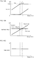
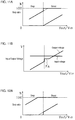
JP S62-18970A - In the above-described conventional voltage converter, when, for example, step-down conversion is switched to step-up conversion, it is preferable as shown in
FIG. 10A that the duty ratio of the step-up PWM signal start increasing from 0% at the same time when the duty ratio of the step-down PWM signal reaches 100%. Furthermore, at that time, it is preferable that the output voltage Vout smoothly increase as shown inFIG. 10B , and the output current continues to flow constantly (seamlessly) as shown inFIG. 10C . - Although determination of switching from step-down conversion to step-up conversion is possible by comparing the input voltage Vin with the output voltage Vout, there is the problem that a voltage drop (
FIG. 10A ) of the output voltage Vout that is caused by the circuit elements within the voltage converter, and temperature change and variation of the circuit element need to be taken into consideration. - For example, if, as shown in
FIG. 11A , the switching from step-down conversion to step-up conversion is performed too early, the voltage will suddenly be boosted and a portion PA in which the output voltage increases discontinuously is created, as shown inFIG. 11B . - Furthermore, if, as shown in
FIG. 12A , the switching from step-down conversion to step-up conversion is performed too late, the voltage boost is delayed accordingly and thus a portion PB in which the output voltage does not increase is created, as shown inFIG. 12B . - The present invention was made in view of the above-described circumstances, and it is an object of the present invention to provide a voltage converter in which switching between step-down conversion and step-up conversion is performed seamlessly, without being affected by a voltage drop of a circuit element and temperature change and variation of the circuit element at the time of the switching between step-down conversion and step-up conversion.
- A voltage converter according to the present invention subjects an input voltage to step-down conversion or step-up conversion to obtain a target voltage, and outputs the obtained voltage, the voltage converter including: a step-down switching element and a step-up switching element that are respectively configured to perform, with PWM control, switching of the input voltage, and switching between the input voltage and a fixed potential in order to increase or decrease the input voltage; a step-down PWM signal generation circuit configured to detect a difference between an output voltage obtained by subjecting the input voltage to the step-down conversion and a step-down target voltage, and to generate a PWM signal for use in the PWM control of the step-down switching element based on the detected difference; a step-up PWM signal generation circuit configured to detect a difference between an output voltage obtained by subjecting the input voltage to the step-up conversion and a step-up target voltage, and to generate a PWM signal for use in the PWM control of the step-up switching element based on the detected difference; and means for making the step-down target voltage, which is a target for the control by the step-down PWM signal generation circuit, larger by a predetermined amount than the step-up target voltage, which is a target for the control by the step-up PWM signal generation circuit.
- In this voltage converter, the step-down switching element and the step-up switching element, which are to perform switching, respectively perform, with PWM control, switching of an input voltage, and switching between the input voltage and a fixed potential in order to increase or decrease the input voltage, subject the input voltage to step-down conversion or step-up conversion to obtain a target voltage, and output the obtained voltage.
- The step-down PWM signal generation circuit detects a difference between an output voltage obtained by subjecting the input voltage to the step-down conversion and the step-down target voltage, and generates a PWM signal for use in the PWM control of the step-down switching element based on the detected difference. The step-up PWM signal generation circuit detects a difference between an output voltage obtained by subjecting the input voltage to the step-up conversion and the step-up target voltage, and generates a PWM signal for use in the PWM control of the step-up switching element based on the detected difference. The increasing means increases the step-down target voltage, which is a target for the control by the step-down PWM signal generation circuit, by a predetermined amount larger than the step-up target voltage, which is a target for the control by the step-up PWM signal generation circuit. Accordingly, a state in which the duty ratio of the PWM signal generated by the step-up PWM signal generation circuit is larger than a lower limit, and a state in which the duty ratio of the PWM signal generated by the step-down PWM signal generation circuit is smaller than an upper limit occur at the same time.
- According to the voltage converter of the present invention, it is possible to realize a voltage converter in which switching between step-down conversion and step-up conversion is performed seamlessly, without being affected by a voltage drop of a circuit element and temperature change and variation of the circuit element at the time of the switching between step-down conversion and step-up conversion.
-
-
FIG. 1 is a circuit diagram illustrating a configuration of a voltage converter according to an embodiment of the present invention. -
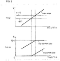
FIG. 2 is a characteristic diagram illustrating target voltages and duty ratios of the voltage converter according to the present invention. -
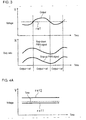
FIG. 3 is a diagram illustrating an operation of the voltage converter. -
FIG. 4A is a diagram illustrating an operation of the voltage converter according to the present invention. -
FIG. 4B is a diagram illustrating an operation of the voltage converter according to the present invention. -
FIG. 4C is diagram illustrating an operation of the voltage converter according to the present invention. -
FIG. 5 is a diagram illustrating an operation of the voltage converter according to the present invention. -
FIG. 6 is a diagram illustrating an operation of the voltage converter according to the present invention. -
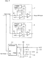
FIG. 7 is a circuit diagram illustrating an internal configuration of a control unit of a voltage converter according to an embodiment of the present invention. -
FIG. 8 is a circuit diagram illustrating an example of a configuration of a conventional voltage converter. -
FIG. 9 is a characteristic diagram illustrating the duty ratio of the conventional voltage converter. -
FIG. 10A is a diagram illustrating an example of the operation of the conventional voltage converter. -
FIG. 10B is a diagram illustrating an example of the operation of the conventional voltage converter. -
FIG. 10C is a diagram illustrating an example of the operation of the conventional voltage converter. -
FIG. 11A is a diagram illustrating an example of the operation of the conventional voltage converter. -
FIG. 11B is a diagram illustrating an example of the operation of the conventional voltage converter. -
FIG. 12A is a diagram illustrating an example of the operation of the conventional voltage converter. -
FIG. 12B is a diagram illustrating an example of the operation of the conventional voltage converter. - Hereinafter, the present invention will be described with reference to the drawings illustrating embodiments thereof.
-
FIG. 1 is a circuit diagram illustrating a configuration of a voltage converter according toEmbodiment 1 of the present invention. - In this voltage converter, a DC input voltage Vin is supplied to the drain of an N-
channel type MOSFET 2, and the source of theFET 2 is connected to one terminal of acoil 1 and the cathode of adiode 4. The anode of thediode 4 is grounded and the other termination of thecoil 1 is connected to the drain of an N-channel type MOSFET 3 and the anode of adiode 5. - The source of the
FET 3 is grounded, and the anode of thediode 5 is connected to the positive terminal of a smoothing capacitor C3, and the negative terminal of the smoothing capacitor C3 is grounded. - The gate of the
FET 2 is connected to a step-down PWMsignal generation circuit 8, the gate of theFET 3 is connected to a step-up PWMsignal generation circuit 7, and theFETs signal generation circuit 8 and the step-up PWMsignal generation circuit 7. - An output voltage Vout of the voltage converter is output across the two terminals of the smoothing capacitor C3, and the input voltage Vin and the output voltage Vout are detected and read by a
control unit 10 including a microcomputer. Furthermore, the output voltage Vout is supplied to the step-down PWMsignal generation circuit 8 and the step-up PWMsignal generation circuit 7. - The step-up PWM
signal generation circuit 7 includes anerror amplifier 13 that has an inverting input terminal to which the output voltage Vout is supplied via a resistor R1 and a non-inverting input terminal to which a target voltage ref1 (step-up target voltage) is supplied from thecontrol unit 10, and a triangularwave generator circuit 12 that oscillates and generates a triangular wave signal W1. Furthermore, a comparator 11 is provided that has an inverting input terminal to which the triangular wave signal W1 is supplied from the triangularwave generator circuit 12 and a non-inverting input terminal to which an output signal from theerror amplifier 13 is supplied, and supplies an output signal to the gate of theFET 3. - A negative feedback circuit in which a resistor R4 is connected in parallel to a resistor R3 and a capacitor C1, which are connected in series, is externally added to the
error amplifier 13, and the gain of theerror amplifier 13 is small. - The step-down PWM
signal generation circuit 8 includes anerror amplifier 23 that has an inverting input terminal to which the output voltage Vout is supplied via a resistor R2 and a non-inverting input terminal to which a target voltage ref2 (step-down target voltage) is supplied from thecontrol unit 10, and a triangularwave generator circuit 22 that oscillates and generates a triangular wave signal W2. Furthermore, acomparator 21 is provided that has an inverting input terminal to which the triangular wave signal W2 is supplied from the triangularwave generator circuit 22 and a non-inverting input terminal to which an output signal from theerror amplifier 23 is supplied, and supplies an output signal to the gate of theFET 2. - A negative feedback circuit in which a resistor R6 is connected in parallel to a resistor R5 and a capacitor C2, which are connected in series, is externally added to the
error amplifier 23, and the gain of theerror amplifier 23 is small. - The
control unit 10 controls the target voltage ref1 of the step-up PWMsignal generation circuit 7 and the target voltage ref2 of the step-down PWMsignal generation circuit 8 by adding a predetermined amount of difference, so that ref1 < ref2 is satisfied. However, the difference between the target voltages ref1 and ref2 is assumed to be sufficiently smaller than the crest values of the triangular wave signals W1 and W2. - Accordingly, as shown in
FIG. 2 , the state in which the duty ratio of a PWM signal generated by the step-up PWMsignal generation circuit 7 is greater than the lower limit (0%), and the state in which the duty ratio of a PWM signal generated by the step-down PWMsignal generation circuit 8 is smaller than the upper limit (100%) occur at the same time, and in this situation in which these states are occurring, switching between step-up conversion and step-down conversion is performed. - If the step-up PWM
signal generation circuit 7 and the step-down PWMsignal generation circuit 8 would operate individually and the target voltages ref were the same, an increase and a decrease in the duty ratios of a step-up PWM signal and a step-down PWM signal would be synchronized as shown inFIG. 3 , and thus there would be the risk that both circuits wholly amplify the gain and oscillate. This oscillation can be avoided by controlling the target voltages ref1 and ref2 by adding a predetermined amount of difference, so that ref1 < ref2 is satisfied. - In the voltage converter having such a configuration, by letting the output signals of the
error amplifiers - When the output voltage Vout is higher than the target voltages ref1 and ref2, the outputs of the
error amplifiers - When the output voltage Vout is lower than the target voltages ref1 and ref2, both the step-up PWM
signal generation circuit 7 and the step-down PWMsignal generation circuit 8 operate to increase the duty ratios and boost the output voltage Vout. When the output voltage Vout is higher than the target voltages ref1 and ref2, both the step-up PWMsignal generation circuit 7 and the step-down PWMsignal generation circuit 8 operate to decrease the duty ratios and drop the output voltage Vout. - In both cases where the output voltage Vout is lower than the target voltages ref1 and ref2, and is higher than the target voltages ref1 and ref2, the output voltage Vout changes toward the target voltages ref1 and ref2, and in both cases, the output voltage Vout is between the target voltages ref1 and ref2.
- In the case where the output voltage Vout is between target voltages ref1 and ref2 as shown in
FIG. 4A , if the output voltage Vout is close to the target voltage ref1, the output of theerror amplifier 13 of the step-up PWMsignal generation circuit 7 changes slightly but the step-down PWMsignal generation circuit 8 increases the duty ratio because the output voltage Vout is lower than the target voltage ref2 (FIG. 4B ). With the increase in the duty ratio of the step-down PWMsignal generation circuit 8, the output voltage Vout becomes much higher than the target voltage ref1, and the step-up PWMsignal generation circuit 7 decreases the duty ratio (FIG. 4C ). - On the other hand, in the case where the output voltage Vout is between the target voltages ref1 and ref2 as shown in
FIG. 4A , if the output voltage Vout is close to the target voltage ref2, the output of theerror amplifier 23 of the step-down PWMsignal generation circuit 8 changes slightly but the step-up PWMsignal generation circuit 7 decreases the duty ratio because the output voltage Vout is higher than the target voltage ref1 (FIG. 4C ). With the decrease in the duty ratio of the step-up PWMsignal generation circuit 7, the output voltage Vout becomes much lower than the target voltage ref2, and the step-down PWMsignal generation circuit 8 increases the duty ratio (FIG. 4B ). - Accordingly, when the output voltage Vout is between the target voltages ref1 and ref2, increases and decreases in the duty ratios of the step-up PWM
signal generation circuit 7 and the step-down PWMsignal generation circuit 8 are in the opposite directions to each other. - If the gains of the
error amplifiers signal generation circuit 7 decreases completely, or the state in which the duty ratio of the step-down PWMsignal generation circuit 8 increases completely, converging to the step-up operation or the step-down operation depending on the dimensional relationship of the current input voltage Vin and target voltages ref1 and ref2. - If the input voltage Vin is higher than the target voltage ref2, the output voltage Vout and the target voltage ref2 are in the equilibrium state when the duty ratio of the step-up PWM
signal generation circuit 7 is a lower limit (for example, 0%) and the duty ratio of the step-down PWMsignal generation circuit 8 is a suitable value. The voltage converter is in the state of executing the step-down operation. - If the input voltage Vin is lower than the target voltage ref1, the output voltage Vout and the target voltage ref1 is in the equilibrium state when the duty ratio of the step-down PWM
signal generation circuit 8 is at an upper limit (for example, 100%) and the duty ratio of the step-up PWMsignal generation circuit 7 has a suitable value. The voltage converter is in the state of executing the step-up operation. - As described above, as shown in
FIG. 5 , when the output voltage Vout is between the target voltages ref1 and ref2, increases and decreases in the duty ratios of the step-up PWM signal and the step-down PWM signal are in the opposite directions to each other, and the output voltage Vout changes slightly (gain decrease), making it possible to prevent the voltage converter from oscillating. - When any one of the duty ratios of the step-up PWM signal and the step-down PWM signal reaches the upper limit or the lower limit, the operation is stabilized at the output voltage Vout of the other target value, and thus, as shown in
FIG. 6 , it is possible to switch seamlessly between the step-down conversion and the step-up conversion. - Note that if the step-up PWM
signal generation circuit 7 and the step-down PWMsignal generation circuit 8 operate individually, there will be numerous combinations of the duty ratios of the step-up PWM signal and the step-down PWM signal in order to obtain a given output voltage Vout. However, this problem can be solved by setting the lower limit for the duty ratio of the step-up PWM signal to 0% and the upper limit for the duty ratio of the step-down PWM signal to 100% in the above-described method. - Assuming that the duty ratio of the step-up PWM signal is Dboost, and the duty ratio of the step-down PWM signal is Ddrop, the relationship between the input voltage Vin and the output voltage Vout is given as follows:


- In the state in which the duty ratio is not 100% or 0%, the
FETs -
FIG. 7 is a circuit diagram illustrating an internal configuration of acontrol unit 10 of a voltage converter according toEmbodiment 2 of the present invention. - This
control unit 10 includes amicrocomputer 24 that is supplied with an input voltage Vin and an output voltage Vout individually and reads them. Themicrocomputer 24 sets target voltages based on the read input voltage Vin and output voltage Vout, generates a PWM signal in order to obtain the target voltages, and performs switching of an NPN-type transistor Tr based on the generated PWM signal. - The emitter of the transistor Tr is grounded, and the collector thereof is connected to a control power supply via resistors R14 and R11. A voltage-dividing circuit of the resistors R11, R12, and R13, a voltage-dividing circuit of the resistors R11, R12, and R16, and a capacitor C4, and a voltage-dividing circuit of the resistors R11 and R15, and a capacitor C5 are formed between the control power supply and ground terminals.
- A target voltage ref1 is obtained from the positive terminal of the capacitor C4, and is supplied to the non-inverting input terminal of the
error amplifier 13. A target voltage ref2 is obtained from the positive terminal of the capacitor C5, and is supplied to the non-inverting input terminal of theerror amplifier 23. - The
microcomputer 24 performs switching of the transistor Tr based on the generated PWM signal to generate predetermined voltages in the voltage-dividing circuit, and the target voltages ref1 and ref2 having a predetermined amount of difference are generated with the corresponding voltage-dividing circuits based on the generated voltages. Other configurations and operations are the same as the configurations and operations ofEmbodiment 1 described above, and thus descriptions thereof are omitted. - The present invention is applicable to a voltage converter that is configured to boost or drop a voltage in a power supply device installed in a vehicle.
-
- 1 Coil
- 2,3 FET
- 4, 5 Diode
- 7 Step-up PWM signal generation circuit
- 8 Step-down PWM signal generation circuit
- 10 Control unit (means for making a voltage larger by a predetermined amount)
- 11, 21 Comparator
- 12, 22 Triangular wave generator circuit
- 13, 23 Error amplifier
- C3 Smoothing capacitor
Claims (1)
- A voltage converter that subjects an input voltage to step-down conversion or step-up conversion to obtain a target voltage, and outputs the obtained voltage, the voltage converter comprising:a step-down switching element and a step-up switching element that are respectively configured to perform, with PWM control, switching of the input voltage, and switching between the input voltage and a fixed potential with PWM control in order to increase or decrease the input voltage; a step-down PWM signal generation circuit configured to detect a difference between an output voltage obtained by subjecting the input voltage to the step-down conversion and a step-down target voltage, and to generate a PWM signal for use in the PWM control of the step-down switching element based on the detected difference;a step-up PWM signal generation circuit configured to detect a difference between an output voltage obtained by subjecting the input voltage to the step-up conversion and a step-up target voltage, and to generate a PWM signal for use in the PWM control of the step-up switching element based on the detected difference; andmeans for making the step-down target voltage, which is a target for the control by the step-down PWM signal generation circuit, larger by a predetermined amount than the step-up target voltage, which is a target for the control by the step-up PWM signal generation circuit.
Applications Claiming Priority (2)
| Application Number | Priority Date | Filing Date | Title |
|---|---|---|---|
| JP2013101593A JP2014222969A (en) | 2013-05-13 | 2013-05-13 | Voltage conversion device |
| PCT/JP2014/061461 WO2014185240A1 (en) | 2013-05-13 | 2014-04-23 | Voltage converter |
Publications (2)
| Publication Number | Publication Date |
|---|---|
| EP3007344A1 true EP3007344A1 (en) | 2016-04-13 |
| EP3007344A4 EP3007344A4 (en) | 2016-12-14 |
Family
ID=51898220
Family Applications (1)
| Application Number | Title | Priority Date | Filing Date |
|---|---|---|---|
| EP14797754.0A Withdrawn EP3007344A4 (en) | 2013-05-13 | 2014-04-23 | VOLTAGE CONVERTER |
Country Status (5)
| Country | Link |
|---|---|
| US (1) | US20160134190A1 (en) |
| EP (1) | EP3007344A4 (en) |
| JP (1) | JP2014222969A (en) |
| CN (1) | CN105247771B (en) |
| WO (1) | WO2014185240A1 (en) |
Families Citing this family (2)
| Publication number | Priority date | Publication date | Assignee | Title |
|---|---|---|---|---|
| JP7127412B2 (en) * | 2018-08-02 | 2022-08-30 | 株式会社オートネットワーク技術研究所 | In-vehicle backup power supply control device and in-vehicle backup power supply device |
| JP7561310B2 (en) | 2020-12-07 | 2024-10-04 | 株式会社オートネットワーク技術研究所 | In-vehicle power supply |
Family Cites Families (12)
| Publication number | Priority date | Publication date | Assignee | Title |
|---|---|---|---|---|
| JPS6218970A (en) | 1985-07-17 | 1987-01-27 | Matsushita Electric Ind Co Ltd | power supply |
| JPH0670486U (en) * | 1993-03-12 | 1994-09-30 | 東光株式会社 | Buck-boost DC-DC converter |
| EP1381135A4 (en) * | 2001-04-17 | 2006-07-19 | Matsushita Electric Industrial Co Ltd | BATTERY-OPERATED ELECTRONIC DEVICE AND MOBILE COMMUNICATION DEVICE |
| JP2003180072A (en) * | 2001-08-07 | 2003-06-27 | Seiko Instruments Inc | Buck-boost switching regulator control circuit and buck-boost switching regulator |
| JP4054714B2 (en) * | 2003-04-28 | 2008-03-05 | 株式会社リコー | Buck-boost DC-DC converter |
| US6936997B2 (en) * | 2003-08-11 | 2005-08-30 | Semiconductor Components Industries, Llc | Method of forming a high efficiency power controller |
| JP4306534B2 (en) * | 2004-05-25 | 2009-08-05 | 株式会社デンソー | Crew protection device |
| JP4957122B2 (en) * | 2006-08-22 | 2012-06-20 | 株式会社ニコン | Power supply circuit and imaging apparatus |
| TWI392989B (en) * | 2008-06-03 | 2013-04-11 | Richtek Technology Corp | Buck-boost switching regulator and control method thereof |
| JP4725641B2 (en) * | 2008-12-17 | 2011-07-13 | 日本テキサス・インスツルメンツ株式会社 | Buck-boost switching regulator |
| US8698463B2 (en) * | 2008-12-29 | 2014-04-15 | Enpirion, Inc. | Power converter with a dynamically configurable controller based on a power conversion mode |
| JP2012029362A (en) | 2010-07-20 | 2012-02-09 | Dsp Oyo Gijutsu Kenkyusho:Kk | Power supply circuit |
-
2013
- 2013-05-13 JP JP2013101593A patent/JP2014222969A/en active Pending
-
2014
- 2014-04-23 CN CN201480026632.3A patent/CN105247771B/en not_active Expired - Fee Related
- 2014-04-23 EP EP14797754.0A patent/EP3007344A4/en not_active Withdrawn
- 2014-04-23 WO PCT/JP2014/061461 patent/WO2014185240A1/en not_active Ceased
- 2014-04-23 US US14/890,291 patent/US20160134190A1/en not_active Abandoned
Also Published As
| Publication number | Publication date |
|---|---|
| EP3007344A4 (en) | 2016-12-14 |
| JP2014222969A (en) | 2014-11-27 |
| WO2014185240A1 (en) | 2014-11-20 |
| CN105247771B (en) | 2018-09-07 |
| CN105247771A (en) | 2016-01-13 |
| US20160134190A1 (en) | 2016-05-12 |
Similar Documents
| Publication | Publication Date | Title |
|---|---|---|
| US10601318B2 (en) | Switching converter using pulse-frequency modulation and current-mode control | |
| US9515550B2 (en) | Inductor current zero-crossing detection method and circuit and switching power supply thereof | |
| US9431906B2 (en) | Voltage converter circuit and associated control method to improve transient performance | |
| US10243463B2 (en) | Non-inverting buck-boost converter control | |
| US8866464B2 (en) | Systems and methods for real time current sense for a switching converter | |
| US10476391B2 (en) | Voltage converting device | |
| US20150028830A1 (en) | Current-mode buck converter and electronic system using the same | |
| US10686374B2 (en) | Control apparatus for power conversion apparatus | |
| CN111869072B (en) | A control circuit of a voltage conversion circuit | |
| US20050007086A1 (en) | Switching regulator control circuit | |
| US20110221407A1 (en) | Dc-dc converter and control method thereof | |
| JP6154584B2 (en) | Power supply device, and in-vehicle device and vehicle using the same | |
| US20090184699A1 (en) | Power supply apparatus and power supply method | |
| CN109997301A (en) | Control program for DC-DC electric power converter | |
| US20070040537A1 (en) | PWM/burst mode switching regulator with automatic mode change | |
| US12027980B2 (en) | Adaptive minimum duty cycle design to extend operational voltage range for DCDC converters | |
| KR20120137243A (en) | Switching regulator | |
| JP2006149067A (en) | DC-DC converter | |
| US11075579B2 (en) | Switching converter, switching time generation circuit and switching time control method thereof | |
| CN111384851B (en) | Control method and device of DC-DC converter | |
| JP2005261011A (en) | Switching regulator and switching regulator control method | |
| JP2013247574A (en) | Pwm signal generation circuit and semiconductor device | |
| US10224815B2 (en) | Voltage converter having a step-up and step-down adjustment circuit | |
| JP2016167896A (en) | DC / DC converter | |
| US20160134190A1 (en) | Voltage converter |
Legal Events
| Date | Code | Title | Description |
|---|---|---|---|
| PUAI | Public reference made under article 153(3) epc to a published international application that has entered the european phase |
Free format text: ORIGINAL CODE: 0009012 |
|
| 17P | Request for examination filed |
Effective date: 20151211 |
|
| AK | Designated contracting states |
Kind code of ref document: A1 Designated state(s): AL AT BE BG CH CY CZ DE DK EE ES FI FR GB GR HR HU IE IS IT LI LT LU LV MC MK MT NL NO PL PT RO RS SE SI SK SM TR |
|
| AX | Request for extension of the european patent |
Extension state: BA ME |
|
| DAX | Request for extension of the european patent (deleted) | ||
| A4 | Supplementary search report drawn up and despatched |
Effective date: 20161116 |
|
| RIC1 | Information provided on ipc code assigned before grant |
Ipc: H02M 3/158 20060101ALI20161110BHEP Ipc: H02M 3/155 20060101AFI20161110BHEP |
|
| STAA | Information on the status of an ep patent application or granted ep patent |
Free format text: STATUS: EXAMINATION IS IN PROGRESS |
|
| 17Q | First examination report despatched |
Effective date: 20191213 |
|
| STAA | Information on the status of an ep patent application or granted ep patent |
Free format text: STATUS: THE APPLICATION HAS BEEN WITHDRAWN |
|
| 18W | Application withdrawn |
Effective date: 20200330 |