EP3002844A1 - Built in test circuit for transient voltage suppressor devices - Google Patents
Built in test circuit for transient voltage suppressor devices Download PDFInfo
- Publication number
- EP3002844A1 EP3002844A1 EP15184595.5A EP15184595A EP3002844A1 EP 3002844 A1 EP3002844 A1 EP 3002844A1 EP 15184595 A EP15184595 A EP 15184595A EP 3002844 A1 EP3002844 A1 EP 3002844A1
- Authority
- EP
- European Patent Office
- Prior art keywords
- test
- control circuit
- node
- transient voltage
- test switch
- Prior art date
- Legal status (The legal status is an assumption and is not a legal conclusion. Google has not performed a legal analysis and makes no representation as to the accuracy of the status listed.)
- Withdrawn
Links
Images


Classifications
-
- G—PHYSICS
- G01—MEASURING; TESTING
- G01R—MEASURING ELECTRIC VARIABLES; MEASURING MAGNETIC VARIABLES
- G01R31/00—Arrangements for testing electric properties; Arrangements for locating electric faults; Arrangements for electrical testing characterised by what is being tested not provided for elsewhere
- G01R31/28—Testing of electronic circuits, e.g. by signal tracer
- G01R31/282—Testing of electronic circuits specially adapted for particular applications not provided for elsewhere
- G01R31/2827—Testing of electronic protection circuits
-
- G—PHYSICS
- G01—MEASURING; TESTING
- G01R—MEASURING ELECTRIC VARIABLES; MEASURING MAGNETIC VARIABLES
- G01R19/00—Arrangements for measuring currents or voltages or for indicating presence or sign thereof
- G01R19/0084—Measuring voltage only
-
- H—ELECTRICITY
- H02—GENERATION; CONVERSION OR DISTRIBUTION OF ELECTRIC POWER
- H02H—EMERGENCY PROTECTIVE CIRCUIT ARRANGEMENTS
- H02H9/00—Emergency protective circuit arrangements for limiting excess current or voltage without disconnection
- H02H9/04—Emergency protective circuit arrangements for limiting excess current or voltage without disconnection responsive to excess voltage
- H02H9/042—Emergency protective circuit arrangements for limiting excess current or voltage without disconnection responsive to excess voltage comprising means to limit the absorbed power or indicate damaged over-voltage protection device
-
- H—ELECTRICITY
- H02—GENERATION; CONVERSION OR DISTRIBUTION OF ELECTRIC POWER
- H02H—EMERGENCY PROTECTIVE CIRCUIT ARRANGEMENTS
- H02H9/00—Emergency protective circuit arrangements for limiting excess current or voltage without disconnection
- H02H9/04—Emergency protective circuit arrangements for limiting excess current or voltage without disconnection responsive to excess voltage
- H02H9/041—Emergency protective circuit arrangements for limiting excess current or voltage without disconnection responsive to excess voltage using a short-circuiting device
Definitions
- the present invention relates generally to transient voltage suppressor (TVS) devices, and specifically to a system and method for performing built-in test (BIT) of TVS devices.
- TVS transient voltage suppressor
- BIT built-in test
- TVS devices are often utilized, for example, to protect circuitry from lightning strikes and other transients.
- TVS devices are often used to protect control circuitry onboard aircraft from these high voltage/current transients.
- a TVS device will turn on at a certain voltage, depending on the specific device, and then clamp the signal line at that voltage, called the clamping voltage, and therefore protect any connected circuitry. Under normal operation, the TVS device does not affect the circuit operation. Often times, a higher clamping voltage is required which may necessitate multiple TVS devices to be configured in series, thus clamping the connected circuitry with a higher clamping voltage and ensuring that the TVS devices do not clamp during normal operation.
- a built-in test system (claim 1) includes a control circuit, a transient voltage suppressor circuit, and a test switch.
- the control circuit is configured to receive a signal
- the transient voltage suppressor circuit includes first and second transient voltage suppressors connected in series between the signal and ground.
- the test switch is connected to selectively conduct current between the signal and a node between the first and second transient voltage suppressors.
- the control circuit is configured to control the test switch to test the first and second transient voltage suppressors.
- a method includes controlling, by a control circuit, a test switch to an OFF state to deny current from a signal to a node between first and second transient voltage suppressors.
- the first and second transient voltage suppressors are connected in series between the first signal and ground.
- the method further includes sampling, by the control circuit, a first sample voltage value at the node, controlling, by the control circuit, the test switch to an ON state to conduct current from the signal to the node, sampling, by the control circuit, a second sample voltage value at the node, and verifying, by the control circuit, functionality of the first and second transient voltage suppressors based upon the first and second sample voltages values.
- a built-in test system and method is disclosed herein for verifying operation of transient voltage suppressor (TVS) devices.
- Protection circuits for lightning and other high voltage/current transients onboard aircraft include a plurality of TVS devices configured in series between an operating signal and ground.
- a switch may be operably connected between the operating signal and a node between two of the plurality of TVS devices. The voltage at that node is provided as an input to the control circuit.
- the control circuit may first sample the wraparound voltage while the switch is in an OFF state.
- the control circuit may then turn the switch to an ON state and again sample the wraparound voltage.
- the first sampled voltage is compared with a first expected voltage value and the second sampled voltage is compared with a second expected voltage value. These expected voltage values may be calculated by the control circuit.
- the functionality of the TVS devices may be determined based upon both the first and second comparisons. In this way, the operability of the TVS devices may be determined during system operation.
- FIG. 1 is a circuit diagram illustrating system 10 for performing built-in test (BIT) of TVS device circuit 12.
- System 10 includes TVS device circuit 12, control circuit 14, test switch 16, resistor 18, and external circuit 20.
- TVS circuit 12 includes TVS devices 22a-22n.
- Control circuit 14 includes signal input/output 24, BIT control output 26, and TVS wraparound 28. External circuit 20 also receives the signal on input/output 24.
- TVS devices 22a-22n are any transient voltage suppressors, such as, for example, TVS diodes (also known as Transzorbs®).
- Control circuit 14 is any electronic control system circuity and may include, for example, a microprocessor, a field programmable gate-array (FPGA), an application specific integrated circuit (ASIC) and/or any other electronic circuit.
- Test switch 16 may be, for example, a metal-oxide-semiconductor field-effect transistor (MOSFET), insulated gate bipolar transistor (IGBT), or any other electrically controlled switch.
- TVS device circuit 12 may be utilized, for example, to provide lightning or other high voltage/current transient protection for control circuit 14 and external circuit 20. Onboard aircraft, for example, lightning strikes may generate a large overvoltage within the electric systems. To accommodate these large voltage transients, TVS devices 22a-22n may be connected in series to create a desired clamping or standoff voltage. Several TVS devices 22a-22n may be utilized in order to achieve a sufficient standoff voltage and reduce the dissipated power of each TVS device 22a-22n. Therefore, the total number of devices 22a-22n that are utilized in TVS device circuit 12 may be determined by, for example, the breakdown voltage of each device 22a-22n and the desirable clamping voltage for system 10. Each device 22a-22n may have a similar breakdown voltage, or each device 22a-22n may be sized differently depending upon the specific application.
- Test switch 16 is implemented to provide built-in test (BIT) for TVS device circuit 12.
- test switch 16 is a MOSFET and connected to selectively allow current to flow from signal input/output 24, through resistor 18 and through TVS device 22a to ground.
- BIT control output 26 is provided to the gate of test switch 16, the voltage at signal input/output 24 is connected to the drain of test switch 16, and resistor 18 is connected to the source of test switch 16.
- Resistor 18 is connected between the source of test switch 16 and TVS wraparound 28. Resistor 18 is any resistor and may be selected such that the resistance provides desirable current draw and power dissipation for system 10.
- BIT control output 26 is such that test switch 16 is in an OFF state.
- BIT control output 26 may be active low such that test switch 16 is in an OFF state and does not conduct between its source and drain.
- control circuit 14 may sample the voltage on TVS wraparound 28. Based upon the leakage current of TVS devices 22a-22n and the voltage on signal input/output 24, a first voltage value may be determined for the wraparound voltage on TVS wraparound 28.
- Control circuit 14 may compare the actual voltage on TVS wraparound 28 with the first voltage value. If the voltage on TVS wraparound 28 is not within a range of the first voltage value, control circuit 14 indicates that the voltage ratio between TVS devices 22a-22n is incorrect.
- control circuit 14 controls test switch 16 to the ON state to further test TVS device circuit 12.
- control circuit 14 may, for example, provide an "active high" signal to turn test switch 16 to an ON state in order to conduct current from signal input/output 24 to TVS wraparound 28.
- Resistor 18 may be sized such that the current conducted through test switch 16 is high enough for TVS device 22a to exceed breakdown and conduct significant current. Therefore, a second expected voltage value on TVS wraparound 28 is the working voltage of TVS device 22a.
- Control circuit 14 compares the second expected voltage value with the actual voltage on TVS wraparound 28 to test the functionality of TVS device 22a. If the voltage on TVS wraparound 28 is not within a range of the second expected voltage value, control circuit 14 indicates a failed test.
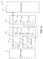
- FIG. 2 is a circuit diagram illustrating system 110 for providing BIT for multiple TVS device circuits 112a and 112b. Common components between FIGS. 1 and 2 may be implemented in a similar manner.
- System 110 includes TVS device circuits 112a and 112b, control circuit 14, test switch 16, and external circuit 20.
- TVS device circuit 112a includes TVS devices 122a-122n and is implemented to protect circuitry connected to signal line 124a.
- TVS device circuit 112b includes TVS devices 132a-132n and is implemented to protected circuitry connected to signal line 124b.
- Diode 130a and resistor 118a are connected in series between the source of test switch 16 and TVS wraparound 128 a.
- Diode 130b and resistor 118b are connected in series between the drain of test switch 16 and TVS wraparound 128b.
- Diodes 130a and 130b are implemented such that both TVS device circuits 112a and 112b may be tested utilizing a single test switch 16. Voltage values may be determined for both TVS wraparounds 128a and 128b for both states of test switch 16. These values may be based at least in part upon the voltage on signal line 124a, leakage currents of TVS devices 122a-122n and 132a-132n and working voltages of TVS devices 122a-122n and 132a-132n. In this way, TVS device circuits 112a and 112b may be tested in a similar manner to that of the embodiment illustrated in FIG. 1 .
- FIG. 3 is a flowchart illustrating method 200 of performing BIT for TVS device circuits.
- control circuit 14 commands test switch 16 to an OFF state.
- Control circuit 14 samples a first voltage value at TVS wraparound 28.
- control circuit 14 commands test switch 16 to an ON state.
- Control circuit 14 samples a second voltage value at TVS wraparound 28.
- the first voltage value is compared to a first expected value and the second voltage value is compared to the second expected voltage value. If the first voltage value is within a range of the first expected voltage value and the second voltage value is within a range of the second expected voltage value, method 200 proceeds to step 208 and indicates a successful test. If the first voltage value is not within a range of the first expected voltage value and/or the second voltage value is not within a range of the second expected voltage value, method 200 proceeds to step 210 and indicates a failed test.
- a failed test may indicate various deficiencies in TVS device circuit 12. If the voltage on TVS wraparound 28 was within a range of the first expected voltage value while test switch 16 was OFF and the voltage on TVS wraparound 28 was not within a range of the second expected voltage value while test switch 16 was ON, then the voltage ratio of TVS devices 22a-22n is correct, but the BIT test was not successful. TVS devices 22a-22n may be implemented incorrectly, or TVS device 22a is damaged or degraded. If the voltage on TVS wraparound 28 was not within a range of the first expected voltage value while test switch 16 was OFF and the voltage on TVS wraparound 28 was within a range of the second expected voltage value while test switch 16 was ON, then the BIT test was unsuccessful.
- the voltage ratio between TVS devices 22a-22n is incorrect, but TVS device 22a is functioning properly. Therefore, one of TVS devices 22b-22n is not functioning properly. If the voltage on TVS wraparound 28 was not within a range of the first expected voltage value while test switch 16 was OFF and the voltage on TVS wraparound 28 was not within a range of the second expected voltage value while test switch 16 was ON, then BIT test was not successful. The voltage ratio of TVS devices 22a-22n is incorrect, and TVS device 22a is not functioning properly. Therefore, at least TVS device 22a is not functioning, but potentially several other TVS devices 22b-22n may also be functioning incorrectly.
- control circuit 14 may be utilized by control circuit 14 for an example implementation of the embodiment shown in FIG. 1 to determine first and second expected voltage values for TVS wraparound 28. These calculations assume only two transient voltage suppressors 22a and 22b in series.
- V A 1 V in - V 1
- i leak 1 i leakfull 1 ⁇ 0.2 ⁇ V A 1 V W 1 + 0.8 ⁇ V A 1 V W 1 2
- i leak 2 i leakfull 2 ⁇ 0.2 ⁇ V A 2 V W 2 + 0.8 ⁇ V A 2 V W 2 2
- Control circuit 14 may utilize this value to determine a first expected voltage value for TVS wraparound 28 while test switch 16 is in an OFF state.
- the expected voltage value for TVS wraparound 28 while test switch 16 is in an ON state will be equal to the working voltage of transient voltage suppressor 22a. Using these two expected voltage values, control circuit 14 is able to test transient voltage suppressors 22a-22n during normal system operation.
- a built-in test system includes a control circuit, a transient voltage suppressor circuit, and a test switch.
- the control circuit is configured to receive a signal
- the transient voltage suppressor circuit includes first and second transient voltage suppressors connected in series between the signal and ground.
- the test switch is connected to selectively conduct current between the signal and a node between the first and second transient voltage suppressors.
- the control circuit is configured to control the test switch to test the first and second transient voltage suppressors.
- the built-in test system of the preceding paragraph can optionally include, additionally and/or alternatively, any one or more of the following features, configurations and/or additional components:
- control circuit is further configured to test the first and second transient voltage suppressors based upon a first sampled voltage value at the first node when the test switch is in an OFF state and based upon a second sampled voltage value at the first node when the test switch is in an ON state.
- control circuit is further configured to determine a first expected voltage value for the first node when the test switch is in the OFF position and a second expected voltage value for the first node when the test switch is in the ON position, and wherein the first and second expected voltage values are based upon the first signal and the first and second transient voltage suppressors.
- controller tests the first and second transient voltage suppressors by comparing the first sampled voltage value to the first expected voltage value and by comparing the second sampled voltage value to the second expected voltage value.
- a further embodiment of any of the foregoing built-in test systems wherein a first resistor is connected between an output of the test switch and the first node.
- a further embodiment of any of the foregoing built-in test systems wherein a third transient voltage suppressor is connected in series between the first signal and the first transient suppressor.
- a further embodiment of any of the foregoing built-in test systems wherein a third transient voltage suppressor is connected in series between the second transient voltage suppressor and the ground.
- a further embodiment of any of the foregoing built-in test systems further including a second transient voltage suppressor circuit comprising third and fourth transient voltage suppressors connected in series between a second signal and the ground.
- the test switch is connected to selectively conduct current between the first signal and a second node between the third and fourth transient voltage suppressors.
- the control circuit is further configured to test the third and fourth transient voltage suppressors based upon a third sampled voltage value at the second node when the test switch is in the OFF state and based upon a fourth sampled voltage value at the second node when the test switch is in the ON state.
- a further embodiment of any of the foregoing built-in test systems further including a first diode and first resistor connected in series between an output of the test switch and the first node, and a second diode and second resistor connected in series between the output of the test switch and the second node.
- control circuit is configured to control the test switch to an OFF state during normal system operation.
- a method includes controlling, by a control circuit, a test switch to an OFF state to deny current from a signal to a node between first and second transient voltage suppressors.
- the first and second transient voltage suppressors are connected in series between the first signal and ground.
- the method further includes sampling, by the control circuit, a first sample voltage value at the node, controlling, by the control circuit, the test switch to an ON state to conduct current from the signal to the node, sampling, by the control circuit, a second sample voltage value at the node, and verifying, by the control circuit, functionality of the first and second transient voltage suppressors based upon the first and second sample voltages values.
- the method of the preceding paragraph can optionally include, additionally and/or alternatively, any one or more of the following features, configurations and/or additional components:
- controlling, by the control circuit, the test switch to the OFF state further comprises controlling the test switch to the OFF state to further deny current from the first signal to a second node between third and fourth transient voltage suppressors, and wherein the third and fourth transient voltage suppressors are connected in series between a second signal and ground.
- the method further includes sampling, by the control circuit, a third sample voltage value at the second node while the test switch is in the OFF state.
- controlling, by the control circuit, the test switch to the ON state further comprises controlling the test switch to the ON state to further conduct current from the first signal to the second node.
- the method further includes sampling, by the control circuit, a fourth sample voltage value at the second node while the test switch is in the ON state, and verifying, by the control circuit, functionality of the third and fourth transient voltage suppressors based upon the third and fourth sample voltage values.
Landscapes
- Engineering & Computer Science (AREA)
- Physics & Mathematics (AREA)
- General Physics & Mathematics (AREA)
- Power Engineering (AREA)
- General Engineering & Computer Science (AREA)
- Tests Of Electronic Circuits (AREA)
Abstract
Description
- The present invention relates generally to transient voltage suppressor (TVS) devices, and specifically to a system and method for performing built-in test (BIT) of TVS devices.
- TVS devices are often utilized, for example, to protect circuitry from lightning strikes and other transients. TVS devices are often used to protect control circuitry onboard aircraft from these high voltage/current transients. A TVS device will turn on at a certain voltage, depending on the specific device, and then clamp the signal line at that voltage, called the clamping voltage, and therefore protect any connected circuitry. Under normal operation, the TVS device does not affect the circuit operation. Often times, a higher clamping voltage is required which may necessitate multiple TVS devices to be configured in series, thus clamping the connected circuitry with a higher clamping voltage and ensuring that the TVS devices do not clamp during normal operation.
- For series connected TVS devices onboard an aircraft, for example, it is not presently possible to verify proper functionality of TVS devices in-flight. It is desirable to verify TVS device functionality in-flight to ensure proper functionality prior to a transient event.
- A built-in test system (claim 1) includes a control circuit, a transient voltage suppressor circuit, and a test switch. The control circuit is configured to receive a signal, and the transient voltage suppressor circuit includes first and second transient voltage suppressors connected in series between the signal and ground. The test switch is connected to selectively conduct current between the signal and a node between the first and second transient voltage suppressors. The control circuit is configured to control the test switch to test the first and second transient voltage suppressors.
- A method (claim 13) includes controlling, by a control circuit, a test switch to an OFF state to deny current from a signal to a node between first and second transient voltage suppressors. The first and second transient voltage suppressors are connected in series between the first signal and ground. The method further includes sampling, by the control circuit, a first sample voltage value at the node, controlling, by the control circuit, the test switch to an ON state to conduct current from the signal to the node, sampling, by the control circuit, a second sample voltage value at the node, and verifying, by the control circuit, functionality of the first and second transient voltage suppressors based upon the first and second sample voltages values.
-
-
FIG. 1 is a circuit diagram illustrating a system for performing built-in test (BIT) for a transient voltage suppressor (TVS) device circuit. -
FIG. 2 is a circuit diagram illustrating a system for providing BIT for multiple TVS device circuits. -
FIG. 3 is a flowchart illustrating a method of performing BIT for TVS device circuits. - A built-in test system and method is disclosed herein for verifying operation of transient voltage suppressor (TVS) devices. Protection circuits for lightning and other high voltage/current transients onboard aircraft, for example, include a plurality of TVS devices configured in series between an operating signal and ground. A switch may be operably connected between the operating signal and a node between two of the plurality of TVS devices. The voltage at that node is provided as an input to the control circuit. The control circuit may first sample the wraparound voltage while the switch is in an OFF state. The control circuit may then turn the switch to an ON state and again sample the wraparound voltage. The first sampled voltage is compared with a first expected voltage value and the second sampled voltage is compared with a second expected voltage value. These expected voltage values may be calculated by the control circuit. The functionality of the TVS devices may be determined based upon both the first and second comparisons. In this way, the operability of the TVS devices may be determined during system operation.
-
FIG. 1 is a circuit diagramillustrating system 10 for performing built-in test (BIT) ofTVS device circuit 12.System 10 includesTVS device circuit 12,control circuit 14,test switch 16,resistor 18, andexternal circuit 20. TVScircuit 12 includesTVS devices 22a-22n.Control circuit 14 includes signal input/output 24,BIT control output 26, andTVS wraparound 28.External circuit 20 also receives the signal on input/output 24.TVS devices 22a-22n are any transient voltage suppressors, such as, for example, TVS diodes (also known as Transzorbs®).Control circuit 14 is any electronic control system circuity and may include, for example, a microprocessor, a field programmable gate-array (FPGA), an application specific integrated circuit (ASIC) and/or any other electronic circuit.Test switch 16 may be, for example, a metal-oxide-semiconductor field-effect transistor (MOSFET), insulated gate bipolar transistor (IGBT), or any other electrically controlled switch. -
TVS device circuit 12 may be utilized, for example, to provide lightning or other high voltage/current transient protection forcontrol circuit 14 andexternal circuit 20. Onboard aircraft, for example, lightning strikes may generate a large overvoltage within the electric systems. To accommodate these large voltage transients,TVS devices 22a-22n may be connected in series to create a desired clamping or standoff voltage.Several TVS devices 22a-22n may be utilized in order to achieve a sufficient standoff voltage and reduce the dissipated power of eachTVS device 22a-22n. Therefore, the total number ofdevices 22a-22n that are utilized inTVS device circuit 12 may be determined by, for example, the breakdown voltage of eachdevice 22a-22n and the desirable clamping voltage forsystem 10. Eachdevice 22a-22n may have a similar breakdown voltage, or eachdevice 22a-22n may be sized differently depending upon the specific application. -
Test switch 16 is implemented to provide built-in test (BIT) forTVS device circuit 12. In the embodiment illustrated inFIG. 1 ,test switch 16 is a MOSFET and connected to selectively allow current to flow from signal input/output 24, throughresistor 18 and throughTVS device 22a to ground.BIT control output 26 is provided to the gate oftest switch 16, the voltage at signal input/output 24 is connected to the drain oftest switch 16, andresistor 18 is connected to the source oftest switch 16.Resistor 18 is connected between the source oftest switch 16 andTVS wraparound 28.Resistor 18 is any resistor and may be selected such that the resistance provides desirable current draw and power dissipation forsystem 10. - During normal system operation,
BIT control output 26 is such thattest switch 16 is in an OFF state. For example,BIT control output 26 may be active low such thattest switch 16 is in an OFF state and does not conduct between its source and drain. Whentest switch 16 is in the OFF state,control circuit 14 may sample the voltage onTVS wraparound 28. Based upon the leakage current ofTVS devices 22a-22n and the voltage on signal input/output 24, a first voltage value may be determined for the wraparound voltage onTVS wraparound 28.Control circuit 14 may compare the actual voltage onTVS wraparound 28 with the first voltage value. If the voltage onTVS wraparound 28 is not within a range of the first voltage value,control circuit 14 indicates that the voltage ratio betweenTVS devices 22a-22n is incorrect. - Following test of
TVS device circuit 12 whiletest switch 16 is OFF,control circuit 14controls test switch 16 to the ON state to further testTVS device circuit 12. Onoutput 26,control circuit 14 may, for example, provide an "active high" signal to turntest switch 16 to an ON state in order to conduct current from signal input/output 24 toTVS wraparound 28.Resistor 18 may be sized such that the current conducted throughtest switch 16 is high enough forTVS device 22a to exceed breakdown and conduct significant current. Therefore, a second expected voltage value onTVS wraparound 28 is the working voltage ofTVS device 22a.Control circuit 14 compares the second expected voltage value with the actual voltage onTVS wraparound 28 to test the functionality ofTVS device 22a. If the voltage onTVS wraparound 28 is not within a range of the second expected voltage value,control circuit 14 indicates a failed test. -
FIG. 2 is a circuitdiagram illustrating system 110 for providing BIT for multipleTVS device circuits FIGS. 1 and2 may be implemented in a similar manner.System 110 includesTVS device circuits control circuit 14,test switch 16, andexternal circuit 20.TVS device circuit 112a includesTVS devices 122a-122n and is implemented to protect circuitry connected to signalline 124a.TVS device circuit 112b includesTVS devices 132a-132n and is implemented to protected circuitry connected to signalline 124b.Diode 130a andresistor 118a are connected in series between the source oftest switch 16 and TVS wraparound 128 a.Diode 130b andresistor 118b are connected in series between the drain oftest switch 16 and TVS wraparound 128b. -
Diodes TVS device circuits single test switch 16. Voltage values may be determined for bothTVS wraparounds test switch 16. These values may be based at least in part upon the voltage onsignal line 124a, leakage currents ofTVS devices 122a-122n and 132a-132n and working voltages ofTVS devices 122a-122n and 132a-132n. In this way,TVS device circuits FIG. 1 . - With continued reference to
FIG. 1 ,FIG. 3 is aflowchart illustrating method 200 of performing BIT for TVS device circuits. Atstep 202,control circuit 14 commands testswitch 16 to an OFF state.Control circuit 14 samples a first voltage value atTVS wraparound 28. Atstep 204,control circuit 14 commands testswitch 16 to an ON state.Control circuit 14 samples a second voltage value atTVS wraparound 28. Atstep 206, the first voltage value is compared to a first expected value and the second voltage value is compared to the second expected voltage value. If the first voltage value is within a range of the first expected voltage value and the second voltage value is within a range of the second expected voltage value,method 200 proceeds to step 208 and indicates a successful test. If the first voltage value is not within a range of the first expected voltage value and/or the second voltage value is not within a range of the second expected voltage value,method 200 proceeds to step 210 and indicates a failed test. - At
step 210, a failed test may indicate various deficiencies inTVS device circuit 12. If the voltage onTVS wraparound 28 was within a range of the first expected voltage value whiletest switch 16 was OFF and the voltage onTVS wraparound 28 was not within a range of the second expected voltage value whiletest switch 16 was ON, then the voltage ratio ofTVS devices 22a-22n is correct, but the BIT test was not successful.TVS devices 22a-22n may be implemented incorrectly, orTVS device 22a is damaged or degraded. If the voltage onTVS wraparound 28 was not within a range of the first expected voltage value whiletest switch 16 was OFF and the voltage onTVS wraparound 28 was within a range of the second expected voltage value whiletest switch 16 was ON, then the BIT test was unsuccessful. The voltage ratio betweenTVS devices 22a-22n is incorrect, butTVS device 22a is functioning properly. Therefore, one ofTVS devices 22b-22n is not functioning properly. If the voltage onTVS wraparound 28 was not within a range of the first expected voltage value whiletest switch 16 was OFF and the voltage onTVS wraparound 28 was not within a range of the second expected voltage value whiletest switch 16 was ON, then BIT test was not successful. The voltage ratio ofTVS devices 22a-22n is incorrect, andTVS device 22a is not functioning properly. Therefore, atleast TVS device 22a is not functioning, but potentially severalother TVS devices 22b-22n may also be functioning incorrectly. - The following equations may be utilized by
control circuit 14 for an example implementation of the embodiment shown inFIG. 1 to determine first and second expected voltage values forTVS wraparound 28. These calculations assume only twotransient voltage suppressors - The following values are defined:
- VA1 is the voltage drop across
transient voltage suppressors 22b. - VA2 is the voltage drop across
transient voltage suppressor 22a. - VW1 is the working voltage of
voltage suppressors 22b. - VW2 is the working voltage of
transient voltage suppressor 22a. - ileak is the leakage current that will flow through
transient voltage suppressors - ileakfull is the leakage current of
transient voltage suppressors - Vin is the voltage on
signal line 24. - V1 is the voltage at
TVS wraparound 28. - Using these definitions, the following equations may be utilized to determine first and second expected voltage values for TVS wraparound 28:


- Because
transient voltage suppressors 


- Let the following constants be defined:


- Therefore, solving for V1:

- One of these values will be out of range for the application and can be discarded.
Control circuit 14 may utilize this value to determine a first expected voltage value forTVS wraparound 28 while test switch 16 is in an OFF state. The expected voltage value forTVS wraparound 28 while test switch 16 is in an ON state will be equal to the working voltage oftransient voltage suppressor 22a. Using these two expected voltage values,control circuit 14 is able to testtransient voltage suppressors 22a-22n during normal system operation. - The following are non-exclusive descriptions of possible embodiments of the present invention.
- A built-in test system includes a control circuit, a transient voltage suppressor circuit, and a test switch. The control circuit is configured to receive a signal, and the transient voltage suppressor circuit includes first and second transient voltage suppressors connected in series between the signal and ground. The test switch is connected to selectively conduct current between the signal and a node between the first and second transient voltage suppressors. The control circuit is configured to control the test switch to test the first and second transient voltage suppressors.
- The built-in test system of the preceding paragraph can optionally include, additionally and/or alternatively, any one or more of the following features, configurations and/or additional components:
- A further embodiment of the foregoing built-in test system, wherein the control circuit is further configured to test the first and second transient voltage suppressors based upon a first sampled voltage value at the first node when the test switch is in an OFF state and based upon a second sampled voltage value at the first node when the test switch is in an ON state.
- A further embodiment of any of the foregoing built-in test systems, wherein the control circuit is further configured to determine a first expected voltage value for the first node when the test switch is in the OFF position and a second expected voltage value for the first node when the test switch is in the ON position, and wherein the first and second expected voltage values are based upon the first signal and the first and second transient voltage suppressors.
- A further embodiment of any of the foregoing built-in test systems, wherein the controller tests the first and second transient voltage suppressors by comparing the first sampled voltage value to the first expected voltage value and by comparing the second sampled voltage value to the second expected voltage value.
- A further embodiment of any of the foregoing built-in test systems, wherein a first resistor is connected between an output of the test switch and the first node.
- A further embodiment of any of the foregoing built-in test systems, wherein a third transient voltage suppressor is connected in series between the first signal and the first transient suppressor.
- A further embodiment of any of the foregoing built-in test systems, wherein a third transient voltage suppressor is connected in series between the second transient voltage suppressor and the ground.
- A further embodiment of any of the foregoing built-in test systems, further including a second transient voltage suppressor circuit comprising third and fourth transient voltage suppressors connected in series between a second signal and the ground. The test switch is connected to selectively conduct current between the first signal and a second node between the third and fourth transient voltage suppressors. The control circuit is further configured to test the third and fourth transient voltage suppressors based upon a third sampled voltage value at the second node when the test switch is in the OFF state and based upon a fourth sampled voltage value at the second node when the test switch is in the ON state.
- A further embodiment of any of the foregoing built-in test systems, further including a first diode and first resistor connected in series between an output of the test switch and the first node, and a second diode and second resistor connected in series between the output of the test switch and the second node.
- A further embodiment of any of the foregoing built-in test systems, wherein the first, second, third and fourth transient voltage suppressors are transient voltage suppression diodes.
- A further embodiment of any of the foregoing built-in test systems, wherein the first and second transient voltage suppressor circuits are high voltage/current transients and/or lightning protection circuits for an aircraft.
- A further embodiment of any of the foregoing built-in test systems, wherein the control circuit is configured to control the test switch to an OFF state during normal system operation.
- A method includes controlling, by a control circuit, a test switch to an OFF state to deny current from a signal to a node between first and second transient voltage suppressors. The first and second transient voltage suppressors are connected in series between the first signal and ground. The method further includes sampling, by the control circuit, a first sample voltage value at the node, controlling, by the control circuit, the test switch to an ON state to conduct current from the signal to the node, sampling, by the control circuit, a second sample voltage value at the node, and verifying, by the control circuit, functionality of the first and second transient voltage suppressors based upon the first and second sample voltages values.
- The method of the preceding paragraph can optionally include, additionally and/or alternatively, any one or more of the following features, configurations and/or additional components:
- A further embodiment of the foregoing method, wherein controlling, by the control circuit, the test switch to the OFF state further comprises controlling the test switch to the OFF state to further deny current from the first signal to a second node between third and fourth transient voltage suppressors, and wherein the third and fourth transient voltage suppressors are connected in series between a second signal and ground. The method further includes sampling, by the control circuit, a third sample voltage value at the second node while the test switch is in the OFF state.
- A further embodiment of any of the foregoing methods, wherein controlling, by the control circuit, the test switch to the ON state further comprises controlling the test switch to the ON state to further conduct current from the first signal to the second node. The method further includes sampling, by the control circuit, a fourth sample voltage value at the second node while the test switch is in the ON state, and verifying, by the control circuit, functionality of the third and fourth transient voltage suppressors based upon the third and fourth sample voltage values.
- While the invention has been described with reference to an exemplary embodiment(s), it will be understood by those skilled in the art that various changes may be made and equivalents may be substituted for elements thereof without departing from the scope of the invention. In addition, many modifications may be made to adapt a particular situation or material to the teachings of the invention without departing from the essential scope thereof. Therefore, it is intended that the invention not be limited to the particular embodiment(s) disclosed, but that the invention will include all embodiments falling within the scope of the appended claims.
Claims (15)
- A built-in test system (10) comprising:a control circuit (14) configured to receive a first signal;a first transient voltage suppressor circuit (12) comprising first and second transient voltage suppressors connected in series between the first signal and ground; anda test switch (16) connected to selectively conduct current between the first signal and a first node between the first and second transient voltage suppressors, wherein the control circuit is configured to control the test switch to test the first and second transient voltage suppressors.
- The built-in test system (10) of claim 1, wherein the control circuit(14) is further configured to test the first and second transient voltage suppressors based upon a first sampled voltage value at the first node when the test switch (16) is in an OFF state and based upon a second sampled voltage value at the first node when the test switch (16) is in an ON state.
- The built-in test system (10) of claim 2, wherein the control circuit (14) is further configured to determine a first expected voltage value for the first node when the test switch (16) is in the OFF position and a second expected voltage value for the first node when the test switch (16) is in the ON position, and wherein the first and second expected voltage values are based upon the first signal and the first and second transient voltage suppressors.
- The built-in test system (10) of claim 3, wherein the controll circuit (14) tests the first and second transient voltage suppressors by comparing the first sampled voltage value to the first expected voltage value and by comparing the second sampled voltage value to the second expected voltage value.
- The built-in test system (10) of claim 1, wherein a first resistor (18) is connected between an output of the test switch and the first node.
- The built-in test system (10) of claim 1, wherein a third transient voltage suppressor is connected in series between the first signal and the first transient suppressor.
- The built-in test system (10) of claim 1, wherein a third transient voltage suppressor is connected in series between the second transient voltage suppressor and the ground.
- The built-in test system (10) of claim 1, further comprising:a second transient voltage suppressor circuit (112b) comprising third and fourth transient voltage suppressors connected in series between a second signal and the ground;wherein the test switch (16) is connected to selectively conduct current between the first signal and a second node between the third and fourth transient voltage suppressors; andwherein the control circuit (14) is further configured to test the third and fourth transient voltage suppressors based upon a third sampled voltage value at the second node when the test switch (16) is in the OFF state and based upon a fourth sampled voltage value at the second node when the test switch (10) is in the ON state.
- The system (10) of claim 8, further comprising:a first diode (130a) and first resistor (118a) connected in series between an output of the test switch (16) and the first node; anda second diode (130b) and second resistor (118b) connected in series between the output of the test switch and the second node.
- The built-in test system (10) of claim 8, wherein the first, second, third and fourth transient voltage suppressors are transient voltage suppression diodes.
- The built-in test system (10) of claim 8, wherein the first and second transient voltage suppressor circuits are high voltage/current transient and/or lightning protection circuits for an aircraft.
- The built-in test system (10) of claim 1, wherein the control circuit is configured to control the test switch to an OFF state during normal system operation.
- A method comprising:controlling, by a control circuit (14), a test switch (16) to an OFF state to deny current from a first signal to a first node between first and second transient voltage suppressors, wherein the first and second transient voltage suppressors are connected in series between the first signal and ground;sampling, by the control circuit (14), a first sample voltage value at the first node;controlling, by the control circuit (14), the test switch (16) to an ON state to conduct current from the first signal to the first node;sampling, by the control circuit (14), a second sample voltage value at the first node; andverifying, by the control circuit, functionality of the first and second transient voltage suppressors based upon the first and second sample voltages values.
- The method of claim 13, wherein controlling, by the control circuit (14), the test switch (16) to the OFF state further comprises controlling the test switch to the OFF state to further deny current from the first signal to a second node between third and fourth transient voltage suppressors, and wherein the third and fourth transient voltage suppressors are connected in series between a second signal and ground, and wherein the method further comprises:sampling, by the control circuit (14), a third sample voltage value at the second node while the test switch is in the OFF state.
- The method of claim 14, wherein controlling, by the control circuit (14), the test switch (16) to the ON state further comprises controlling the test switch to the ON state to further conduct current from the first signal to the second node, and wherein the method further comprises:sampling, by the control circuit (14), a fourth sample voltage value at the second node while the test switch (16) is in the ON state; andverifying, by the control circuit (14), functionality of the third and fourth transient voltage suppressors based upon the third and fourth sample voltage values.
Applications Claiming Priority (1)
| Application Number | Priority Date | Filing Date | Title |
|---|---|---|---|
| US14/503,937 US9671453B2 (en) | 2014-10-01 | 2014-10-01 | Built in test circuit for transient voltage suppressor devices |
Publications (1)
| Publication Number | Publication Date |
|---|---|
| EP3002844A1 true EP3002844A1 (en) | 2016-04-06 |
Family
ID=54106213
Family Applications (1)
| Application Number | Title | Priority Date | Filing Date |
|---|---|---|---|
| EP15184595.5A Withdrawn EP3002844A1 (en) | 2014-10-01 | 2015-09-10 | Built in test circuit for transient voltage suppressor devices |
Country Status (2)
| Country | Link |
|---|---|
| US (1) | US9671453B2 (en) |
| EP (1) | EP3002844A1 (en) |
Cited By (3)
| Publication number | Priority date | Publication date | Assignee | Title |
|---|---|---|---|---|
| EP3089303A1 (en) * | 2015-04-29 | 2016-11-02 | Hamilton Sundstrand Corporation | Built-in test circuits for transient voltage protection devices |
| CN112147394A (en) * | 2020-09-23 | 2020-12-29 | 珠海格力电器股份有限公司 | Residual voltage detection device |
| EP3772790A1 (en) * | 2019-08-06 | 2021-02-10 | Hamilton Sundstrand Corporation | Transient voltage suppressor bit stimulation |
Families Citing this family (5)
| Publication number | Priority date | Publication date | Assignee | Title |
|---|---|---|---|---|
| US10277028B2 (en) | 2016-04-28 | 2019-04-30 | Continental Automotive Systems, Inc. | Selectable input transient voltage suppressor |
| US10759546B2 (en) | 2017-08-23 | 2020-09-01 | Hamilton Sundstrand Corporation | Transient voltage suppression protection circuit including built in testing and enable-disable functionality |
| CN107918090B (en) * | 2017-10-30 | 2021-03-23 | 武汉海微科技有限公司 | A TVS tube detection system and method |
| KR20230078589A (en) * | 2020-10-02 | 2023-06-02 | 램 리써치 코포레이션 | Voltage Transient Detector and Current Transient Detector |
| FR3154247B1 (en) * | 2023-10-16 | 2025-12-26 | Safran Electronics & Defense | ELECTRONIC SYSTEM PROTECTION AGAINST SURGES |
Citations (4)
| Publication number | Priority date | Publication date | Assignee | Title |
|---|---|---|---|---|
| US5914662A (en) * | 1998-01-23 | 1999-06-22 | Current Technology, Inc. | Circuit and method for indicating the remaining suppressing capacity of a multiple-element transient-voltage protection device |
| DE102011012284A1 (en) * | 2011-02-24 | 2012-08-30 | Knorr-Bremse Systeme für Nutzfahrzeuge GmbH | Overvoltage protection circuit and method for checking an overvoltage protection circuit |
| US20120236447A1 (en) * | 2011-03-14 | 2012-09-20 | Mack Michael P | Input-output esd protection |
| US8649149B1 (en) * | 2011-03-07 | 2014-02-11 | Adtran, Inc. | Dual level surge protector circuit for telecommunication line |
Family Cites Families (5)
| Publication number | Priority date | Publication date | Assignee | Title |
|---|---|---|---|---|
| US6266223B1 (en) * | 1999-06-30 | 2001-07-24 | Tyco Electronics Corporation | Line protector for a communications circuit |
| US7009831B2 (en) * | 2004-02-27 | 2006-03-07 | Microsemi Corporation | PIN or NIP low capacitance transient voltage suppressors and steering diodes |
| US20060152877A1 (en) * | 2005-01-12 | 2006-07-13 | Buzzard Brian W | Transient suppression circuit |
| US8860082B2 (en) * | 2012-07-15 | 2014-10-14 | Richtek Technology Corporation, R.O.C. | Transient voltage suppressor circuit, and diode device therefor and manufacturing method thereof |
| US9383405B2 (en) * | 2013-04-10 | 2016-07-05 | Hamilton Sundstrand Corporation | Transient voltage suppression protection circuit including built in testing |
-
2014
- 2014-10-01 US US14/503,937 patent/US9671453B2/en active Active
-
2015
- 2015-09-10 EP EP15184595.5A patent/EP3002844A1/en not_active Withdrawn
Patent Citations (4)
| Publication number | Priority date | Publication date | Assignee | Title |
|---|---|---|---|---|
| US5914662A (en) * | 1998-01-23 | 1999-06-22 | Current Technology, Inc. | Circuit and method for indicating the remaining suppressing capacity of a multiple-element transient-voltage protection device |
| DE102011012284A1 (en) * | 2011-02-24 | 2012-08-30 | Knorr-Bremse Systeme für Nutzfahrzeuge GmbH | Overvoltage protection circuit and method for checking an overvoltage protection circuit |
| US8649149B1 (en) * | 2011-03-07 | 2014-02-11 | Adtran, Inc. | Dual level surge protector circuit for telecommunication line |
| US20120236447A1 (en) * | 2011-03-14 | 2012-09-20 | Mack Michael P | Input-output esd protection |
Cited By (5)
| Publication number | Priority date | Publication date | Assignee | Title |
|---|---|---|---|---|
| EP3089303A1 (en) * | 2015-04-29 | 2016-11-02 | Hamilton Sundstrand Corporation | Built-in test circuits for transient voltage protection devices |
| US9711960B2 (en) | 2015-04-29 | 2017-07-18 | Hamilton Sundstrand Corporation | Built-in test circuits for transient voltage protection devices |
| EP3772790A1 (en) * | 2019-08-06 | 2021-02-10 | Hamilton Sundstrand Corporation | Transient voltage suppressor bit stimulation |
| US11209475B2 (en) | 2019-08-06 | 2021-12-28 | Hamilton Sundstrand Corporation | Transient voltage suppressor bit stimulation |
| CN112147394A (en) * | 2020-09-23 | 2020-12-29 | 珠海格力电器股份有限公司 | Residual voltage detection device |
Also Published As
| Publication number | Publication date |
|---|---|
| US9671453B2 (en) | 2017-06-06 |
| US20160097803A1 (en) | 2016-04-07 |
Similar Documents
| Publication | Publication Date | Title |
|---|---|---|
| US9671453B2 (en) | Built in test circuit for transient voltage suppressor devices | |
| US8598899B2 (en) | Built-in test for an overvoltage protection circuit | |
| EP3089303B1 (en) | Built-in test circuits for transient voltage protection devices | |
| EP3203251B1 (en) | Shared transient voltage suppressor for protecting multiple load channels of a solid state power controller having built-in-test capability | |
| US10236677B2 (en) | Semiconductor device | |
| US8866489B2 (en) | Test apparatus with power cutoff section having variable maximum and minimum thresholds | |
| US8836338B2 (en) | Switching circuits and methods of testing thereof | |
| EP2549649A1 (en) | Actively clamped transistor circuit | |
| US9214873B2 (en) | Method for operating an electrical power rectifier, as well as an electrical power rectifier | |
| JP7305303B2 (en) | drive and power module | |
| US20150041849A1 (en) | Ignition control short circuit protection | |
| EP2790284A1 (en) | Transient voltage suppression protection circuit including built in testing | |
| US10090672B2 (en) | Shared transient voltage suppressor having built-in-test capability for solid state power controllers | |
| EP3934040A1 (en) | Depletion mode mosfet for overcurrent protection | |
| US9673609B2 (en) | Self-test of over-current fault detection | |
| CA2975741C (en) | Surge protection circuit | |
| US9213055B2 (en) | Semiconductor device | |
| EP3667849A1 (en) | Systems and methods for lightning protection in power distribution modules | |
| EP4152542A1 (en) | Overvoltage protection for high power current fed converters using di(t)/dt sensors | |
| EP2690784A1 (en) | Self-test of over-current fault detection | |
| US20180306856A1 (en) | Testing device and testing method with spike protection | |
| EP3306801A1 (en) | Power conversion device and motor device | |
| US20250105709A1 (en) | Techniques for isolating electrical current from a motor in an electric power steering system | |
| US20250306077A1 (en) | Solid-state pulse generating system and the control system thereof | |
| Pappalardo et al. | The RHRPMICL1A integrated current limiter: Radiation tests and high voltage application |
Legal Events
| Date | Code | Title | Description |
|---|---|---|---|
| PUAI | Public reference made under article 153(3) epc to a published international application that has entered the european phase |
Free format text: ORIGINAL CODE: 0009012 |
|
| AK | Designated contracting states |
Kind code of ref document: A1 Designated state(s): AL AT BE BG CH CY CZ DE DK EE ES FI FR GB GR HR HU IE IS IT LI LT LU LV MC MK MT NL NO PL PT RO RS SE SI SK SM TR |
|
| AX | Request for extension of the european patent |
Extension state: BA ME |
|
| 17P | Request for examination filed |
Effective date: 20161004 |
|
| RBV | Designated contracting states (corrected) |
Designated state(s): AL AT BE BG CH CY CZ DE DK EE ES FI FR GB GR HR HU IE IS IT LI LT LU LV MC MK MT NL NO PL PT RO RS SE SI SK SM TR |
|
| STAA | Information on the status of an ep patent application or granted ep patent |
Free format text: STATUS: EXAMINATION IS IN PROGRESS |
|
| 17Q | First examination report despatched |
Effective date: 20171207 |
|
| STAA | Information on the status of an ep patent application or granted ep patent |
Free format text: STATUS: THE APPLICATION IS DEEMED TO BE WITHDRAWN |
|
| 18D | Application deemed to be withdrawn |
Effective date: 20180619 |