EP2996192A1 - A mobile device having an interior multiband antenna and a partially metal back - Google Patents
A mobile device having an interior multiband antenna and a partially metal back Download PDFInfo
- Publication number
- EP2996192A1 EP2996192A1 EP15184714.2A EP15184714A EP2996192A1 EP 2996192 A1 EP2996192 A1 EP 2996192A1 EP 15184714 A EP15184714 A EP 15184714A EP 2996192 A1 EP2996192 A1 EP 2996192A1
- Authority
- EP
- European Patent Office
- Prior art keywords
- antenna
- conducting
- frequency range
- central portion
- back side
- Prior art date
- Legal status (The legal status is an assumption and is not a legal conclusion. Google has not performed a legal analysis and makes no representation as to the accuracy of the status listed.)
- Granted
Links
Images






Classifications
-
- H—ELECTRICITY
- H01—ELECTRIC ELEMENTS
- H01Q—ANTENNAS, i.e. RADIO AERIALS
- H01Q1/00—Details of, or arrangements associated with, antennas
- H01Q1/12—Supports; Mounting means
- H01Q1/22—Supports; Mounting means by structural association with other equipment or articles
- H01Q1/24—Supports; Mounting means by structural association with other equipment or articles with receiving set
- H01Q1/241—Supports; Mounting means by structural association with other equipment or articles with receiving set used in mobile communications, e.g. GSM
- H01Q1/242—Supports; Mounting means by structural association with other equipment or articles with receiving set used in mobile communications, e.g. GSM specially adapted for hand-held use
- H01Q1/243—Supports; Mounting means by structural association with other equipment or articles with receiving set used in mobile communications, e.g. GSM specially adapted for hand-held use with built-in antennas
-
- H—ELECTRICITY
- H01—ELECTRIC ELEMENTS
- H01Q—ANTENNAS, i.e. RADIO AERIALS
- H01Q1/00—Details of, or arrangements associated with, antennas
- H01Q1/50—Structural association of antennas with earthing switches, lead-in devices or lightning protectors
-
- H—ELECTRICITY
- H01—ELECTRIC ELEMENTS
- H01Q—ANTENNAS, i.e. RADIO AERIALS
- H01Q21/00—Antenna arrays or systems
- H01Q21/28—Combinations of substantially independent non-interacting antenna units or systems
-
- H—ELECTRICITY
- H01—ELECTRIC ELEMENTS
- H01Q—ANTENNAS, i.e. RADIO AERIALS
- H01Q5/00—Arrangements for simultaneous operation of antennas on two or more different wavebands, e.g. dual-band or multi-band arrangements
- H01Q5/30—Arrangements for providing operation on different wavebands
- H01Q5/307—Individual or coupled radiating elements, each element being fed in an unspecified way
- H01Q5/342—Individual or coupled radiating elements, each element being fed in an unspecified way for different propagation modes
- H01Q5/357—Individual or coupled radiating elements, each element being fed in an unspecified way for different propagation modes using a single feed point
- H01Q5/364—Creating multiple current paths
- H01Q5/371—Branching current paths
-
- H—ELECTRICITY
- H01—ELECTRIC ELEMENTS
- H01Q—ANTENNAS, i.e. RADIO AERIALS
- H01Q5/00—Arrangements for simultaneous operation of antennas on two or more different wavebands, e.g. dual-band or multi-band arrangements
- H01Q5/30—Arrangements for providing operation on different wavebands
- H01Q5/378—Combination of fed elements with parasitic elements
-
- H—ELECTRICITY
- H01—ELECTRIC ELEMENTS
- H01Q—ANTENNAS, i.e. RADIO AERIALS
- H01Q9/00—Electrically-short antennas having dimensions not more than twice the operating wavelength and consisting of conductive active radiating elements
- H01Q9/04—Resonant antennas
- H01Q9/30—Resonant antennas with feed to end of elongated active element, e.g. unipole
- H01Q9/42—Resonant antennas with feed to end of elongated active element, e.g. unipole with folded element, the folded parts being spaced apart a small fraction of the operating wavelength
-
- H—ELECTRICITY
- H04—ELECTRIC COMMUNICATION TECHNIQUE
- H04M—TELEPHONIC COMMUNICATION
- H04M1/00—Substation equipment, e.g. for use by subscribers
- H04M1/02—Constructional features of telephone sets
- H04M1/0202—Portable telephone sets, e.g. cordless phones, mobile phones or bar type handsets
Definitions
- the present disclosure describes examples of devices with a predominantly metal and/or predominantly conducting back side in the form of a conducting portion of the back side.
- the back side includes ends that are non-conducting.
- multi-band antennas are located in the interior of the device, for example on an internal chassis, but behind the non-conducting portions of the back side, though connections to an antenna feed and/or a ground plane can run at least partially behind a conducting portion of the back side.
- the conducting portion can comprise a central portion of the back side that separates non-conducting ends. Radiating arms of each of the antennas are located behind the non-conducting portions.
- Each multi-band antenna can resonate in three different frequency ranges including, but not limited to, 710-960 MHz, 1710-2100 MHz and 2300-2700MHz.
- a switch in the device can switch between the antennas, and/or cause both antennas to resonate at the same time depending on whether the device is in an uplink mode or a downlink mode, and/or based on an antenna selection table stored in a memory of the device.
- elements may be described as “configured to” perform one or more functions or “configured for” such functions.
- an element that is configured to perform or configured for performing a function is enabled to perform the function, or is suitable for performing the function, or is adapted to perform the function, or is operable to perform the function, or is otherwise capable of performing the function.
- the back side can further comprise a non-conducting chassis, and the conducting central portion can comprise a conducting sheet attached to the non-conducting chassis, the first non-conducting portion and the second non-conducting portion can each comprise opposite ends of the non-conducting chassis, and the first end edge and the second end edge can comprise opposite end edges of the non-conducting chassis.
- a first radiating arm of the at least two respective radiating arms can be located closer to the conducting central portion than a second radiating arm of the at least two respective radiating arms, and the first radiating arm can be configured to resonate in a lower frequency range than the second radiating arm.
- the first radiating arm and the second radiating arm can be generally parallel to each other, electrically connected by a connecting portion but otherwise separated by a gap, the first radiating arm electrically connected to a ground plane at a respective end and the second radiating arm electrically connected to the one or more antenna feeds.
- interface 124 is configured to correspond with network architecture that is used to implement one or more communication links to the one or more communication networks, including but not limited to any suitable combination of USB (universal serial bus) cables, serial cables, wireless links, cell-phone links, cellular network links (including but not limited to 2G, 2.5G, 3G, 4G+ such as UMTS (Universal Mobile Telecommunications System), GSM (Global System for Mobile Communications), CDMA (Code division multiple access), FDD (frequency division duplexing), LTE (Long Term Evolution), TDD (time division duplexing), TDD-LTE (TDD-Long Term Evolution), TD-SCDMA (Time Division Synchronous Code Division Multiple Access) and the like, wireless data, Bluetooth links, NFC (near field communication) links, WLAN (wireless local area network) links, WiFi links, WiMax links, packet based links, the Internet, analog networks, the PSTN (public switched telephone network), access points, and the like, and/or a combination.
- USB Universal Serial Bus
- serial cables serial cables
- First antenna 111 is generally located on interior chassis 401 behind first non-conducting portion 211 (as depicted in Fig. 5 , described in further detail below).
- second antenna 112 is generally located on interior chassis 401 behind second non-conducting portion 212.
- each of first antenna 111 and second antenna 112 comprises at least two respective radiating arms configured to resonate in at least three frequency ranges.
- one or more antenna feeds 110 are connected to each of first antenna 111 and second antenna 112.
- switch 115 is configured to select one or more of first antenna 111 and second antenna 112 for operation.
- a position of the at least two respective arms of each of first antenna 111 and second antenna 112 are selected to clear conducting central portion 203 of back side 201.
- a position of each of antennas 111, 112 behind non-conducting portions 211, 212 are selected to minimize interference with conducting central portion 203.
- the at least two respective arms of each of first antenna 111 and second antenna 112 do not overlap with conducting central portion 203 (where "clear” is generally understood to mean substantially non-overlapping).
- connection 809 to one more antenna feeds 110 clears conducting central portion 203 of back side 201 (i.e. connection 809 does not overlap conducting central portion 203).
- the "left hand” curves show measured total and radiation efficiency when the successful prototype of device 101 is held in a left hand, away from a head, while the "left hand beside head” show measured total and radiation efficiency when the successful prototype of device 101 is held in a left hand, beside a head.
- the curves of Fig. 13 depicted measured total and radiation efficiency in "use” situations.
Landscapes
- Engineering & Computer Science (AREA)
- Computer Networks & Wireless Communication (AREA)
- Support Of Aerials (AREA)
- Variable-Direction Aerials And Aerial Arrays (AREA)
- Details Of Aerials (AREA)
Abstract
Description
- The specification relates generally to antennas, and specifically to a mobile device having an interior multiband antenna and a partially metal back.
- A MIMO (multiple-input and multiple-output) antenna design of a partial metal housing for 4G handset applications generally includes the antenna working at low, mid and high frequencies (e.g. tri- band) and/or multiband, for example, with a low band being a range of 710-960MHz, a medium band being in a range of 1710-2100MHz, and high band being in a range of 2300-2700MHz. The multi-band design can effectively reduce the number of antennae used in mobile applications. However, MIMO multi-band antenna technology in partial metal housing handsets can be challenging as such multi-band antennas should fit into a partial metal back compact phone with multi-operating frequencies, and good diversity and capacity performance. However, the partial metal back can interfere with the antenna; hence, when the multi-band antennas are put in the partial metal back handset, their performance deteriorates.
- For a better understanding of the various implementations described herein and to show more clearly how they may be carried into effect, reference will now be made, by way of example only, to the accompanying drawings in which:
-
Fig. 1 depicts a front perspective view of f a device that includes a multi-antenna system for mobile handsets with at least a partially metallic back side, according to non-limiting implementations. -
Fig. 2 depicts a schematic diagram of the device ofFig. 1 , according to non-limiting implementations. -
Fig. 3 depicts an exterior perspective view of a back side of the device ofFig. 1 , according to non-limiting implementations. -
Fig. 4 depicts a perspective view of back facing side of an interior chassis of the device ofFig. 1 , including two multi-band antennas, according to non-limiting implementations. -
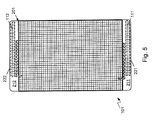
Fig. 5 depicts an exterior perspective view of the back side of the device ofFig. 1 , along with the relative location of the antennas located on the interior chassis, according to non-limiting implementations. -
Fig. 6 depicts a perspective view of front facing side of an interior chassis of the device ofFig. 1 , along with the relative location of the antennas located on the back facing side of the interior chassis, according to non-limiting implementations. -
Fig. 7 depicts a perspective view of an end of the interior chassis comprising a first antenna of the device ofFig. 1 , according to non-limiting implementations. -
Fig. 8 depicts a perspective view of another end the interior chassis comprising a second antenna of the device ofFig. 1 , according to non-limiting implementations. -
Fig. 9 depicts return-loss curves of antennas of a successful prototype of the device ofFig. 1 , according to non-limiting implementations. -
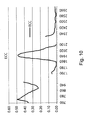
Fig. 10 depicts envelope correlation coefficients as a function of frequency of the successful prototype, according to non-limiting implementations. -
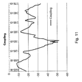
Fig. 11 depicts a coupling curve of the successful prototype, according to non-limiting implementations. -
Fig. 12 depicts free space total and radiation efficiencies of the antennas of the successful prototype, according to non-limiting implementations. -
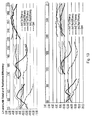
Fig. 13 depicts total and radiation efficiencies of the antennas of the successful prototype in specific use situations, according to non-limiting implementations. -
Fig. 14 depicts an antennas selection table for use in the device ofFig. 1 , according to non-limiting implementations. - The present disclosure describes examples of devices with a predominantly metal and/or predominantly conducting back side in the form of a conducting portion of the back side. The back side includes ends that are non-conducting. In such devices, multi-band antennas are located in the interior of the device, for example on an internal chassis, but behind the non-conducting portions of the back side, though connections to an antenna feed and/or a ground plane can run at least partially behind a conducting portion of the back side. For example, the conducting portion can comprise a central portion of the back side that separates non-conducting ends. Radiating arms of each of the antennas are located behind the non-conducting portions. Each multi-band antenna can resonate in three different frequency ranges including, but not limited to, 710-960 MHz, 1710-2100 MHz and 2300-2700MHz. And a switch in the device can switch between the antennas, and/or cause both antennas to resonate at the same time depending on whether the device is in an uplink mode or a downlink mode, and/or based on an antenna selection table stored in a memory of the device.
- In this specification, elements may be described as "configured to" perform one or more functions or "configured for" such functions. In general, an element that is configured to perform or configured for performing a function is enabled to perform the function, or is suitable for performing the function, or is adapted to perform the function, or is operable to perform the function, or is otherwise capable of performing the function.
- Furthermore, as will become apparent, in this specification certain elements may be described as connected physically, electronically, or any combination thereof, according to context. In general, components that are electrically connected are configured to communicate (that is, they are capable of communicating) by way of electric signals. According to context, two components that are physically coupled and/or physically connected may behave as a single element. In some cases, physically connected elements may be integrally formed, e.g., part of a single-piece article that may share structures and materials. In other cases, physically connected elements may comprise discrete components that may be fastened together in any fashion. Physical connections may also include a combination of discrete components fastened together, and components fashioned as a single piece.
- Furthermore, as will become apparent in this specification, certain antenna components may be described as being configured for generating a resonance at a given frequency and/or resonating at a given frequency and/or having a resonance at a given frequency. In general, an antenna component that is configured to resonate at a given frequency, and the like, can also be described as having a resonant length, a radiation length, a radiating length, an electrical length, and the like, corresponding to the given frequency. The electrical length can be similar to, or different from, a physical length of the antenna component. The electrical length of the antenna component can be different from the physical length, for example by using electronic components to effectively lengthen the electrical length as compared to the physical length. The term electrical length is most often used with respect to simple monopole and/or dipole antennas. The resonant length can be similar to, or different from, the electrical length and the physical length of the antenna component. In general, the resonant length corresponds to an effective length of an antenna component used to generate a resonance at the given frequency; for example, for irregularly shaped and/or complex antenna components that resonate at a given frequency, the resonant length can be described as a length of a simple antenna component, including but not limited to a monopole antenna and a dipole antenna, that resonates at the same given frequency.
- An aspect of the specification provides a device comprising: a back side comprising: a conducting central portion; a first non-conducting portion comprising a first width from first end edge of the back cover to the conducting central portion; and a second non-conducting portion opposite the first non-conducting portion, comprising a second width from a second end edge of the back cover to the conducting central portion, the conducting central portion separating the first non-conducting portion and the second non-conducting portion; an interior chassis covered by the back side; a first antenna located on the interior chassis behind the first non-conducting portion; a second antenna located on the interior chassis behind the second non-conducting portion, each of the first antenna and the second antenna comprising at least two respective radiating arms configured to resonate in at least three frequency ranges; one or more antenna feeds connected to each of the first antenna and the second antenna; and, a switch configured to select one or more of the first antenna and the second antenna for operation.
- The back side can further comprise a non-conducting chassis, and the conducting central portion can comprise a conducting sheet attached to the non-conducting chassis, the first non-conducting portion and the second non-conducting portion can each comprise opposite ends of the non-conducting chassis, and the first end edge and the second end edge can comprise opposite end edges of the non-conducting chassis.
- The at least two respective arms of each of the first antenna and the second antenna clear the conducting central portion of the back side.
- Each of the first antenna and the second antenna can further comprise: a first respective connection to the one more antenna feeds; and a second respective connection to a ground plane.
- Each of the first antenna and the second antenna can further comprise: a first respective connection to the one more antenna feeds; and a second respective connection to a ground plane, each of the first respective connection and the second respective connection can be on opposite sides of a respective antenna radiating structure.
- Each of the first antenna and the second antenna can further comprise: a respective connection to the one more antenna feeds, the respective connection can clear the conducting central portion of the back side.
- Each of the first antenna and the second antenna can further comprise: a respective connection to a ground plane, the respective connection at least partially located behind the conducting central portion of the back side.
- At least a respective portion of one or more of the first antenna and the second antenna can at least partially wrap around a respective end of the interior chassis.
- A first radiating arm of the at least two respective radiating arms can be located closer to the conducting central portion than a second radiating arm of the at least two respective radiating arms, and the first radiating arm can be configured to resonate in a lower frequency range than the second radiating arm. The first radiating arm and the second radiating arm can be generally parallel to each other, electrically connected by a connecting portion but otherwise separated by a gap, the first radiating arm electrically connected to a ground plane at a respective end and the second radiating arm electrically connected to the one or more antenna feeds.
- The first width and the second width can be different from each other.
- The device can further comprise a port through an end of the device adjacent the first antenna, the first antenna clearing the port.
- The device can further comprise an interior conducting plane, each of the at least two respective radiating arms at least partially clearing the interior conducting plane.
- The device can further comprise a memory storing an antenna selection table, and the switch is configured to select one or more of the first antenna and the second antenna for operation based upon the antenna selection table.
- The conducting central portion can cover about 80% of the back side.
- A first one of the at least three frequency ranges can comprise one or more of: a frequency range of about 710MHz to about 960MHz; an LTE (Long-Term Evolution) frequency range; and LTE700 frequency range; a second one of the at least three frequency ranges can comprise one or more of: about 1710 to about 2100MHz, a GSM (Global System for Mobile Communications) frequency range; a CDMA (Code Division Multiple Access) frequency range; a PCS (Personal Communications Service) frequency range; and a UMTS (Universal Mobile Telecommunications System) frequency range; and, a third one of the at least three frequency ranges can comprise one or more of: about 2300 to about 2700MHz, another GSM (Global System for Mobile Communications) frequency range; another CDMA (Code Division Multiple Access) frequency range; another PCS (Personal Communications Service) frequency range; and another UMTS (Universal Mobile Telecommunications System) frequency range.
-
Figs. 1 and2 respectively depict a front perspective view and a schematic diagram of a mobileelectronic device 101, referred to interchangeably hereafter asdevice 101.Device 101 comprises: achassis 109; one ormore antenna feeds 110, afirst antenna 111, and asecond antenna 112; and aswitch 115 configured to select one or more offirst antenna 111 andsecond antenna 112 for operation. Physical configurations ofdevice 101 andantennas -
Device 101 can be any type of electronic device that can be used in a self-contained manner to communicate with one or more communicationnetworks using antennas Device 101 can include, but is not limited to, any suitable combination of electronic devices, communications devices, computing devices, personal computers, laptop computers, portable electronic devices, mobile computing devices, portable computing devices, tablet computing devices, laptop computing devices, desktop phones, telephones, PDAs (personal digital assistants), cellphones, smartphones, e-readers, internet-enabled appliances and the like. Other suitable devices are within the scope of present implementations. Device hence further comprise aprocessor 120, amemory 122, adisplay 126, acommunication interface 124 that can optionally compriseantenna feed 110 and/or switch 115, at least oneinput device 128, aspeaker 132 and amicrophone 134. - It should be emphasized that the shape and structure of
device 101 inFigs. 1 and2 are purely examples, and contemplate a device that can be used for both wireless voice (e.g. telephony) and wireless data communications (e.g. email, web browsing, text, and the like). However,Fig. 1 contemplates a device that can be used for any suitable specialized functions, including, but not limited, to one or more of, telephony, computing, appliance, and/or entertainment related functions. - With reference to
Fig. 1 , an exterior ofdevice 101 is depicted with a front portion ofchassis 109, the corners ofchassis 109 being generally square though, in other implementation, the corners can be rounded and/or any other suitable shape; indeed, the shape and configuration ofdevice 101 depicted inFig. 1 is merely an example and other shapes and configurations are within the scope of present implementations. - With reference to
Figs. 1 and2 ,device 101 comprises at least oneinput device 128 generally configured to receive input data, and can comprise any suitable combination of input devices, including but not limited to a keyboard, a keypad, a pointing device (as depicted inFig. 1 ), a mouse, a track wheel, a trackball, a touchpad, a touch screen and the like. Other suitable input devices are within the scope of present implementations. - Input from
input device 128 is received at processor 120 (which can be implemented as a plurality of processors, including but not limited to one or more central processors (CPUs)).Processor 120 is configured to communicate with amemory 122 comprising a non-volatile storage unit (e.g. Erasable Electronic Programmable Read Only Memory ("EEPROM"), Flash Memory) and a volatile storage unit (e.g. random access memory ("RAM")). Programming instructions that implement the functional teachings ofdevice 101 as described herein are typically maintained, persistently, inmemory 122 and used byprocessor 120 which makes appropriate utilization of volatile storage during the execution of such programming instructions. Those skilled in the art will now recognize thatmemory 122 is an example of computer readable media that can store programming instructions executable onprocessor 120. Furthermore,memory 122 is also an example of a memory unit and/or memory module. -
Memory 122 further stores anapplication 145 that, when processed byprocessor 120, enablesprocessor 120 to controlswitch 115 to switch betweenantennas memory 122storing application 145 is an example of a computer program product, comprising a non-transitory computer usable medium having a computer readable program code adapted to be executed to implement a method, for example a method stored inapplication 145. -
Memory 122 can further store an antenna selection table 146 that can be processed byprocessor 120 so that a decision can be made as to whichantenna switch 115 can be controlled accordingly. Antenna selection table 146 is described in further detail below. -
Processor 120 can be further configured to communicate withdisplay 126, andmicrophone 134 andspeaker 132.Display 126 comprises any suitable one of, or combination of, flat panel displays (e.g. LCD (liquid crystal display), plasma displays, OLED (organic light emitting diode) displays, capacitive or resistive touchscreens, CRTs (cathode ray tubes) and the like.Microphone 134 comprises any suitable microphone for receiving sound and converting to audio data.Speaker 132 comprises any suitable speaker for converting audio data to sound to provide one or more of audible alerts, audible communications from remote communication devices, and the like. In some implementations,input device 128 anddisplay 126 are external todevice 101, withprocessor 120 in communication with each ofinput device 128 anddisplay 126 via a suitable connection and/or link. -
Processor 120 also connects to communication interface 124 (interchangeably referred to interchangeably as interface 124), which can be implemented as one or more radios and/or connectors and/or network adaptors, configured to wirelessly communicate with one or more communication networks (not depicted) viaantennas interface 124 is configured to correspond with network architecture that is used to implement one or more communication links to the one or more communication networks, including but not limited to any suitable combination of USB (universal serial bus) cables, serial cables, wireless links, cell-phone links, cellular network links (including but not limited to 2G, 2.5G, 3G, 4G+ such as UMTS (Universal Mobile Telecommunications System), GSM (Global System for Mobile Communications), CDMA (Code division multiple access), FDD (frequency division duplexing), LTE (Long Term Evolution), TDD (time division duplexing), TDD-LTE (TDD-Long Term Evolution), TD-SCDMA (Time Division Synchronous Code Division Multiple Access) and the like, wireless data, Bluetooth links, NFC (near field communication) links, WLAN (wireless local area network) links, WiFi links, WiMax links, packet based links, the Internet, analog networks, the PSTN (public switched telephone network), access points, and the like, and/or a combination. - Specifically,
interface 124 comprises radio equipment (i.e. a radio transmitter and/or radio receiver) for receiving and transmittingsignals using antennas interface 124 comprisesantenna feed 110 and switch 115, which alternatively can be separate frominterface 124 and/or separate from each other. - As depicted,
device 101 further comprises aport 136 which can include, but is not limited to a USB (Universal Serial Bus) port. - While not depicted,
device 101 can further comprise a ground plane that can be connected to one or more ofantennas - While also not depicted,
device 101 further comprises a power source, not depicted, for example a battery or the like. In some implementations the power source can comprise a connection to a mains power supply and a power adaptor (e.g. and AC-to-DC (alternating current to direct current) adaptor). - In any event, it should be understood that a wide variety of configurations for
device 101 are contemplated. - Furthermore, each of
antennas - In other words, each
antenna - Physical configurations of
device 101,antennas Figs. 3 through 8 . - Attention is next directed to
Fig. 3 which depicts a perspective view of a back ofdevice 101 that includes aback side 201 ofdevice 101.Back side 201 can comprise a component ofchassis 109, and is generally attachable to a remaining portion ofdevice 101, including, but not limited to, a front portion ofchassis 109 depicted inFig. 1 and/or an internal chassis. For example, backside 201 can include a back cover that can be removabley attached todevice 101 so that a battery ofdevice 101 can be accessed. - In any event, back
side 201 comprises a conductingcentral portion 203; a firstnon-conducting portion 211 comprising a first width W1 fromfirst end edge 221 ofback side 201 to conductingcentral portion 203; and a secondnon-conducting portion 212 opposite firstnon-conducting portion 211, comprising a second width W2 from asecond end edge 222 ofback side 201 to conductingcentral portion 203, conductingcentral portion 203 separating firstnon-conducting portion 211 and secondnon-conducting portion 212. Conductingcentral portion 203 can comprise one or more conducting materials, including, but not limited to, one or more metals. However, conducting plastics, conducting polymers, and the like are within the scope of present implementations.Non-conducting portions - In some implementations, first width W1 and second width W2 can be different from each other, while in other implementations, first width W1 and second width W2 can be about the same.
- In some implementations back
side 201 can be flexible so that one or more latches, hooks, and the like ofback side 201 can be undone to remove backside 201 fromdevice 101. - In some implementations, back
side 201 can further comprise a non-conducting chassis, conductingcentral portion 203 comprising a conducting sheet attached to the non-conducting chassis, firstnon-conducting portion 211 and secondnon-conducting portion 212 each comprising opposite ends of the non-conducting chassis, andfirst end edge back side 201 are within the scope of present implementations; for example, eachnon-conducting portion central portion 203 using any combination of attachment devices, glues, and the like. - In some implementations, as depicted, conducting
central portion 203 covers about 80% ofback side 201. However, in other implementations, conductingcentral portion 203 can cover more or less than 80% ofback side 201. However, eachnon-conducting portion antennas central portion 203 can selected so as to not interfere with operation of each ofantennas - Attention is next directed to
Fig. 4 which depicts aninterior chassis 401 ofdevice 101. In general,interior chassis 401 is internal todevice 101 and is covered by backside 201.Interior chassis 401 can comprise a non-conducting material including, but not limited to, plastics, polymers and the like. Furthermore,interior chassis 401 can act as a substrate for other internal components of device including, but not limited toprocessor 120,memory 122,antenna feed 110,interface 124,switch 115 and the like, as well as one or more PCBs (printed circuit boards), computer buses, and the like. Such components can be located in anarea 403, for example behind conductingcentral portion 203 ofback side 201. - While
interior chassis 401 is depicted as continuous, in other implementations,interior chassis 401 can comprise apertures, cut-outs and the like to accommodate other components ofdevice 101. -
First antenna 111 is generally located oninterior chassis 401 behind first non-conducting portion 211 (as depicted inFig. 5 , described in further detail below). Similarly,second antenna 112 is generally located oninterior chassis 401 behind secondnon-conducting portion 212. Further, as described in further detail below, each offirst antenna 111 andsecond antenna 112 comprises at least two respective radiating arms configured to resonate in at least three frequency ranges. Furthermore, one or more antenna feeds 110 are connected to each offirst antenna 111 andsecond antenna 112. In addition,switch 115 is configured to select one or more offirst antenna 111 andsecond antenna 112 for operation. - Attention is next directed to
Fig. 5 , which is substantially similar toFig. 3 , with like elements having like numbers. However, inFig. 5 , positions ofantennas device 101 are depicted in outline to show thatfirst antenna 111 is located behind the firstnon-conducting portion 211 andsecond antenna 112 is located behind the secondnon-conducting portion 212. - In particular, a position of the at least two respective arms of each of
first antenna 111 andsecond antenna 112 are selected to clear conductingcentral portion 203 ofback side 201. In other words, a position of each ofantennas non-conducting portions central portion 203. Hence, the at least two respective arms of each offirst antenna 111 andsecond antenna 112 do not overlap with conducting central portion 203 (where "clear" is generally understood to mean substantially non-overlapping). - Attention is next directed to
Fig. 6 which depicts a side ofinterior chassis 401 that is opposite the side depicted inFig. 4 . In other words, the side ofinterior chassis 401 depicted inFig. 4 faces a back ofdevice 101, while the side ofinterior chassis 401 depicted inFig. 6 faces a front of device 101 (e.g. as depicted inFig. 1 ). In these implementations,device 101 further comprises aninterior conducting plane 601, for example each of the at least two respective radiating arms of each ofantennas interior conducting plane 601. As depicted, interior conductingplane 601 is located on a side ofinterior chassis 401opposite antennas device 101, with one or more antenna feeds 110 connected thereto. In any event, radiating arms ofantenna 112 generally clear (i.e. do not overlap)interior conducting plane 601. However, a portion of interior conductingplane 601 can extend towards an end ofdevice 101, for example an end adjacentfirst antenna 111. Such an extension can be associated with a port ofdevice 101, including, but not limited to, a USB (Universal Serial Bus) port. In these implementations, the portion of interior conductingplane 601 that extends towards the end ofdevice 101 and/or along a port (e.g. port 136), can partially overlap radiating arms ofantenna 111, which can affect the performance ofantenna 111, as described in further detail below. - While interior conducting
plane 601 is depicted as continuous, in other implementations, interior conductingplane 601 can comprise apertures, cut-outs and the like to accommodate other components ofdevice 101. - Attention is next directed to
Fig. 7 , which depicts an end view ofinterior chassis 401showing antenna 111 in detail, as well as dimensions of a successful prototype ofantenna 111. In these implementations,interior chassis 401 comprises a plastic substrate with a thickness of about 6mm at an end ofinterior chassis 401 upon whichantenna 111 is mounted. For example,antenna 111 can comprise a microstrip oninterior chassis 401. As depictedinterior chassis 401 further comprisesport 136 through an end adjacentfirst antenna 111,first antenna 111clearing port 136. - In any event, as seen in
Fig. 7 ,first antenna 111 comprises afirst radiating arm 701 and asecond radiating arm 702. First radiatingarm 701 of the at least two respective radiating arms offirst antenna 111 is located closer to conductingcentral portion 203 thansecond radiating arm 702 of the at least two respective radiating arms,first radiating arm 701 configured to resonate in a lower frequency range thansecond radiating arm 702. In other words,first radiating arm 701 is the requirement value, shorter thansecond radiating arm 702. - Furthermore,
first radiating arm 701 andsecond radiating arm 702 are generally parallel to each other, and electrically connected by a connectingportion 703 but otherwise separated by agap 705,first radiating arm 701 electrically connected to a ground plane (not depicted) at arespective end 707 andsecond radiating arm 702 electrically connected to one or more antenna feeds 110 (not depicted inFig. 7 ) via aconnection 709 which, as depicted, wraps around an end ofinterior chassis 401. - Hence, as depicted
antenna 111 comprises a firstrespective connection 709 to one or more antenna feeds 110; and a secondrespective connection 711 to a ground plane. - Furthermore,
connection 709 to onemore antenna feed 110 clears conductingcentral portion 203 of back side 201 (i.e.connection 709 does not overlap conducting central portion 203). - In addition,
connection 711 to the ground plane can at least partially be located behind conductingcentral portion 203 ofback side 201. In other words,connection 711 can connect end 707 offirst radiating arm 701, which clears conductingcentral portion 203 to the ground plane which can be located behind conductingcentral portion 203. Indeed, in some implementations, conductingcentral portion 203 can comprise the ground plane. - Furthermore, while
antenna 111 comprises a PIFA (Planar Inverted F Antenna) other antenna shapes are within the scope of present implementations that will resonate in similar frequency ranges. In addition, firstrespective connection 709 to one more antenna feeds 110 and secondrespective connection 711 to a ground plane, are appreciated to be located on opposite sides of a respective antenna radiating structure ofantenna 111. In other words,connections arms - From
Fig. 7 , it is further seen thatsecond radiating arm 702 is located along an edge ofinterior chassis 401 and at least partially wraps around one or more sides ofinterior chassis 401, while clearing and/or not overlappingport 136. Indeed,second radiating arm 702 can conform to a geometry of an adjacent end ofinterior chassis 401. - As depicted, in a successful prototype,
first radiating arm 701 has dimensions of about 33 mm long by about 2 mm wide, second radiating arm has dimensions of about 55 mm long by about 7 mm wide, andgap 705 comprises two portions separated byconnection 703, a first portion ofgap 705 having dimensions of about 18 mm long by about 1 mm wide, and a second portion having dimensions of about 14 mm long by about 1 mm wide. Furthermore,connection 711 has dimensions of about 8 mm long by about 2 mm wide. However, other dimensions and configurations that allowantenna 111 to resonate within at least three frequency ranges are within the scope of present implementations. - Attention is next directed to
Fig. 8 , which depicts an end view ofinterior chassis 401showing antenna 112 in detail, as well as dimensions of a successful prototype ofantenna 112. In these implementations,interior chassis 401 comprises a plastic substrate with a thickness of about 6mm at an end ofinterior chassis 401 upon whichantenna 112 is mounted. For example,antenna 112 can comprise a microstrip oninterior chassis 401. In other words,Fig. 8 depicts an opposite end ofinterior chassis 401 as that depicted inFig. 7 . - In any event, as seen in
Fig. 8 ,second antenna 112 comprises afirst radiating arm 801 and asecond radiating arm 802. First radiatingarm 801 of the at least two respective radiating arms ofsecond antenna 112 is located closer to conductingcentral portion 203 thansecond radiating arm 802 of the at least two respective radiating arms,first radiating arm 801 configured to resonate in a lower frequency range thansecond radiating arm 802. In other words,first radiating arm 801 is shorter thansecond radiating arm 802. - Furthermore,
first radiating arm 801 andsecond radiating arm 802 are generally parallel to each other, and electrically connected by a connectingportion 803 but otherwise separated by agap 805,first radiating arm 801 electrically connected to a ground plane (not depicted) at arespective end 807 andsecond radiating arm 802 electrically connected to one or more antenna feeds 110 (not depicted inFig. 8 ) via aconnection 809 which, as depicted, wraps around an end ofinterior chassis 401. - Hence, as depicted
antenna 112 comprises a firstrespective connection 809 to one more antenna feeds 110; and a secondrespective connection 811 to a ground plane. - Furthermore,
connection 809 to one more antenna feeds 110 clears conductingcentral portion 203 of back side 201 (i.e.connection 809 does not overlap conducting central portion 203). - In addition,
connection 811 to the ground plane can at least partially be located behind conductingcentral portion 203 ofback side 201. In other words,connection 811 can connect end 807 offirst radiating arm 801, which clears conductingcentral portion 203 to the ground plane which can be located behind conductingcentral portion 203. Indeed, in some implementations, conductingcentral portion 203 can comprise the ground plane. - Furthermore, while
antenna 112 comprises a PIFA (Planar Inverted F Antenna) other antenna shapes are within the scope of present implementations that will resonate in similar frequency ranges. In addition, firstrespective connection 809 to one more antenna feeds 110 and secondrespective connection 811 to a ground plane, are appreciated to be located on opposite sides of a respective antenna radiating structure ofantenna 112. In other words,connections arms - From
Fig. 8 , it is further seen thatsecond radiating arm 802 is located along an edge ofinterior chassis 401 and at least partially wraps around one or more sides ofinterior chassis 401, while clearing and/or not overlappingport 136. Indeed,second radiating arm 802 can conform to a geometry of an adjacent end ofinterior chassis 401. - As depicted, in a successful prototype of
device 101,first radiating arm 801 has dimensions of about 35 mm long by about 1 mm wide, second radiating arm has dimensions of about 55 mm long by about 7 mm wide, andgap 805 comprises two portions separated byconnection 803, a first portion ofgap 805 having dimensions of about 11 mm long by about 1 mm wide, and a second portion having dimensions of about 23 mm long by about 1 mm wide. Furthermore,connection 811 has dimensions of about 8 mm long by about 1 mm wide. However, other dimensions and configurations that allowantenna 112 to resonate within at least three frequency ranges are within the scope of present implementations. - While each of
antennas antennas antenna antennas Figs. 7 and8 can be due to differences in local electrical environment. For example,first antenna 111 isadjacent port 136 and further has partial overlap with interior conductingplane 601; hence dimensions offirst antenna 111 are different from dimensions ofsecond antenna 112 to account for the effect ofport 136 and/or interior conductingplane 601 onfirst antenna 111. - Further, while there can be one or more antenna feeds 110, each
antenna respective connection antenna feed 110. Hence, eachantenna - Attention is next directed to
Fig. 9 which depicts return-loss curves for specific non-limiting implementations of the successful prototype ofantennas antennas Fig. 9 . Indeed, the various markers shown inFig. 9 show the return-loss for the S11 component at frequencies of 710 MHz, 960 MHz, 1710 MHz, 2100 MHz, 2300 MHz and 2700 MHz, and peaks are clearly located between marker pairs of 710 MHz to 960 MHz, 1710 MHz to 2100 MHz, and 2300 MHz to 2700 MHz, which delineate cellular frequency ranges. - In the successful prototype width W1 was about 10 mm, and width W2 was about 9 mm. Furthermore, clearance of the
interior conducting plane 601 was about 14 mm forantenna 111 and about 12 mm for antenna 112 (i.e. there was about 14mm and 12 mm of non-conducting material on either side of interior conductingplane 601, not including the extension forport 136, upon whichantennas - Attention is next directed to
Figs. 10 and11 , which respectively depicts an envelope correlation coefficient as a function of frequency and coupling as a function of frequency betweenantennas Fig. 10 , the envelope correlation coefficient is less than about 0.5 in each of the frequency ranges of 710-960MHz, 1710-2100MHz and 2300-2700MHz. Envelope correlation coefficients of less than 0.5 are appreciated to be associated with independent sub channels into eachantenna Fig. 11 , coupling betweenantennas antennas antennas antenna antennas - Such good performance of the successful prototype is further shown in
Fig. 12 which depicts free space efficiency as a function of frequency for each of antenna 111 ("Ant1" inFig. 12 , the top set of curves) and antenna 112 ("Ant2" inFig. 12 , the bottom set of curves), and specifically free space total efficiency (solid lines) and free space radiation efficiency (broken lines) as a function of frequency for each ofantenna 111 andantenna 112, in each of the frequency ranges of 710-960MHz, 1710-2100MHz and 2300-2700MHz. The target free space radiation efficiency values for given specifications (including, but not limited to specifications provided by an operator, specifications for a given network, a design specification for a given band, and the like) in each of the frequency ranges are depicted as straight lines. In other words, in the frequency range of 710-960MHz, the target free space radiation efficiency is greater than about -4.50 db, in the frequency range of 1710-2100MHz the target free space radiation efficiency is greater than about -4.00 db, and in the frequency range of 2300-2700MHz the target free space radiation efficiency is greater than about -4.00 db. It is clear that the free space radiation efficiency meets the target specifications in all but the highest frequency range of antenna 111 (i.e. the free space radiation curves are higher than the target value in all but the highest frequency range of antenna 111). In general, total efficiency is the radiation efficiency plus losses for mismatch. Hence, in some implementations, one or more antenna feeds 110 and/orinterface 124 can comprise one or more of a matching circuit and/or a tuning circuit to account for such mismatches. - Performance of the successful prototype is further depicted in
Fig. 13 , which shows left hand ("LH", top sets of curves) and left hand beside head ("LHB", bottom set of curves) total and radiation efficiency for antenna 111 ("Ant1" inFig. 13 ) and antenna 112 ("Ant2" inFig. 13 ), in each of the frequency ranges of 710-960MHz, 1710-2100MHz and 2300-2700MHz, similar toFig. 12 , with a target specification value depicted in each frequency range as a straight line. The "left hand" curves show measured total and radiation efficiency when the successful prototype ofdevice 101 is held in a left hand, away from a head, while the "left hand beside head" show measured total and radiation efficiency when the successful prototype ofdevice 101 is held in a left hand, beside a head. In other words, the curves ofFig. 13 depicted measured total and radiation efficiency in "use" situations. - In any event, it is clear that for most frequencies, the radiated efficiencies are above the target specification.
- Using such measurements, antenna selection table 146 can be populated. For example, attention is next directed to
Fig. 14 , which depicts a non-limiting implementation of an antenna selection table 146. However, while the depicted antenna selection table 146 is organized in a table format, and/or in rows and columns, in other implementations, antenna selection table 146 can be organized in any other format accessible toprocessor 120 to determine whichantenna Fig. 13 , but measured with the successful prototype in a right hand and beside a head. - In any event, antenna selection table 146 depicts, for each indicated frequency range, an average measured efficiency in the frequency range for each of
antenna antenna antenna antennas antennas antennas antennas antenna 111 can be selected for use in this frequency range, and as -5.5 is below the requirement value of -5,antenna 112 is not selected for use. In anyevent processor 120 can determine which frequency range is in use, further determine which use situation applies (e.g. left hand, right hand, beside head, free space etc. based on sensor readings and the like) anduse switch 115 to select one or more ofantennas device 101 to a network) or a downlink mode (i.e. data being downloaded todevice 101 from the network). When in an uplink mode, only one ofantennas antennas - It is further appreciated that SAR (specific absorption rate) can also be measured and used to populate antenna selection table. In other words, when SAR is above a given threshold for a given
antenna antenna - Furthermore, while antenna selection table 146 depicted in
Fig. 14 shows the efficiency values for each ofantennas antennas - In any event, described herein are examples devices with multi-band MIMO antennas that are located behind non-conducting portions of a partially metallic, and/or partially conducting, back cover.
- Those skilled in the art will appreciate that in some implementations, the functionality of
device 101 can be implemented using pre-programmed hardware or firmware elements (e.g., application specific integrated circuits (ASICs), electrically erasable programmable read-only memories (EEPROMs), etc.), or other related components. In other implementations, the functionality ofdevice 101 can be achieved using a computing apparatus that has access to a code memory (not shown) which stores computer-readable program code for operation of the computing apparatus. The computer-readable program code could be stored on a computer readable storage medium which is fixed, tangible and readable directly by these components, (e.g., removable diskette, CD-ROM, ROM, fixed disk, USB drive). Furthermore, it is appreciated that the computer-readable program can be stored as a computer program product comprising a computer usable medium. Further, a persistent storage device can comprise the computer readable program code. It is yet further appreciated that the computer-readable program code and/or computer usable medium can comprise a non-transitory computer-readable program code and/or non-transitory computer usable medium. Alternatively, the computer-readable program code could be stored remotely but transmittable to these components via a modem or other interface device connected to a network (including, without limitation, the Internet) over a transmission medium. The transmission medium can be either a non-mobile medium (e.g., optical and/or digital and/or analog communications lines) or a mobile medium (e.g., microwave, infrared, free-space optical or other transmission schemes) or a combination thereof. - A portion of the disclosure of this patent document contains material which is subject to copyright protection. The copyright owner has no objection to the facsimile reproduction by any one of the patent document or patent disclosure, as it appears in the Patent and Trademark Office patent file or records, but otherwise reserves all copyrights whatsoever.
- Persons skilled in the art will appreciate that there are yet more alternative implementations and modifications possible, and that the above examples are only illustrations of one or more implementations. The scope, therefore, is to be limited by the claims appended here.
Claims (15)
- A device (101) comprising:a back side (201) comprising: a conducting central portion (203); a first non-conducting portion (211) comprising a first width from first end edge of the back cover to the conducting central portion (203); and a second non-conducting portion (212) opposite the first non-conducting portion (211), comprising a second width from a second end edge of the back cover to the conducting central portion (203), the conducting central portion (203) separating the first non-conducting portion (211) and the second non-conducting portion (212);an interior chassis (401) covered by the back side (201);a first antenna (111) located on the interior chassis (401) behind the first non-conducting portion (211);a second antenna (112) located on the interior chassis (401) behind the second non-conducting portion (212), each of the first antenna (111) and the second antenna (112) comprising at least two respective radiating arms configured to resonate in at least three frequency ranges;one or more antenna feeds (110) connected to each of the first antenna (111) and the second antenna (112); and,a switch (115) configured to select one or more of the first antenna (111) and the second antenna (112) for operation.
- The device (101) of claim 1, wherein the back side (201) further comprises a non-conducting chassis, the conducting central portion (203) comprising a conducting sheet attached to the non-conducting chassis, the first non-conducting portion (211) and the second non-conducting portion (212) each comprise opposite ends of the non-conducting chassis, and the first end edge and the second end edge comprises opposite end edges of the non-conducting chassis.
- The device (101) of claim 1 or 2, wherein the at least two respective arms of each of the first antenna (111) and the second antenna (112) clear the conducting central portion (203) of the back side (201).
- The device (101) of any previous claim, wherein each of the first antenna (111) and the second antenna (112) further comprise: a first respective connection to the one more antenna feeds (110); and a second respective connection to a ground plane.
- The device (101) of any previous claim, wherein each of the first antenna (111) and the second antenna (112) further comprise: a first respective connection to the one more antenna feeds (110); and a second respective connection to a ground plane, each of the first respective connection and the second respective connection being on opposite sides of a respective antenna radiating structure.
- The device (101) of any previous claim, wherein each of the first antenna (111) and the second antenna (112) further comprise: a respective connection to the one more antenna feeds (110), the respective connection clearing the conducting central portion (203) of the back side (201).
- The device (101) of any previous claim, wherein each of the first antenna (111) and the second antenna (112) further comprise: a respective connection to a ground plane, the respective connection at least partially located behind the conducting central portion (203) of the back side (201).
- The device (101) of any previous claim, wherein at least a respective portion of one or more of the first antenna (111) and the second antenna (112) at least partially wraps around a respective end of the interior chassis (401).
- The device (101) of any previous claim, wherein a first radiating arm of the at least two respective radiating arms is located closer to the conducting central portion (203) than a second radiating arm of the at least two respective radiating arms, the first radiating arm configured to resonate in a lower frequency range than the second radiating arm.
- The device (101) of claim 8, wherein the first radiating arm and the second radiating arm are generally parallel to each other, electrically connected by a connecting portion but otherwise separated by a gap, the first radiating arm electrically connected to a ground plane at a respective end and the second radiating arm electrically connected to the one or more antenna feeds (110).
- The device (101) of any previous claim, wherein the first width and the second width are different from each other.
- The device (101) of any previous claim, further comprising a port through an end of the device (101) adjacent the first antenna (111), the first antenna (111) clearing the port.
- The device (101) of any previous claim, further comprising an interior conducting plane, each of the at least two respective radiating arms at least partially clearing the interior conducting plane.
- The device (101) of any previous claim, wherein the conducting central portion (203) covers about 80% of the back side (201).
- The device (101) of any previous claim, wherein:a first one of the at least three frequency ranges comprises one or more of: a frequency range of about 710MHz to about 960MHz; an LTE (Long-Term Evolution) frequency range; and LTE700 frequency range;a second one of the at least three frequency ranges comprises one or more of: about 1710 to about 2100MHz, a GSM (Global System for Mobile Communications) frequency range; a CDMA (Code Division Multiple Access) frequency range; a PCS (Personal Communications Service) frequency range; and a UMTS (Universal Mobile Telecommunications System) frequency range; and,a third one of the at least three frequency ranges comprises one or more of: about 2300 to about 2700MHz, another GSM (Global System for Mobile Communications) frequency range; another CDMA (Code Division Multiple Access) frequency range; another PCS (Personal Communications Service) frequency range; and another UMTS (Universal Mobile Telecommunications System) frequency range.
Applications Claiming Priority (1)
| Application Number | Priority Date | Filing Date | Title |
|---|---|---|---|
| US14/486,724 US9882266B2 (en) | 2014-09-15 | 2014-09-15 | Mobile device having an interior multiband antenna and a partially metal back |
Publications (3)
| Publication Number | Publication Date |
|---|---|
| EP2996192A1 true EP2996192A1 (en) | 2016-03-16 |
| EP2996192C0 EP2996192C0 (en) | 2023-06-21 |
| EP2996192B1 EP2996192B1 (en) | 2023-06-21 |
Family
ID=54251924
Family Applications (1)
| Application Number | Title | Priority Date | Filing Date |
|---|---|---|---|
| EP15184714.2A Active EP2996192B1 (en) | 2014-09-15 | 2015-09-10 | A mobile device having an interior multiband antenna and a partially metal back |
Country Status (4)
| Country | Link |
|---|---|
| US (1) | US9882266B2 (en) |
| EP (1) | EP2996192B1 (en) |
| CA (1) | CA2904306C (en) |
| ES (1) | ES2950342T3 (en) |
Families Citing this family (4)
| Publication number | Priority date | Publication date | Assignee | Title |
|---|---|---|---|---|
| KR102120281B1 (en) * | 2016-07-27 | 2020-06-08 | 후아웨이 테크놀러지 컴퍼니 리미티드 | Wireless receiving/transmitting device and base station |
| KR102364559B1 (en) | 2017-03-24 | 2022-02-21 | 삼성전자주식회사 | Electronic device comprising antenna |
| CN112689986A (en) * | 2018-09-17 | 2021-04-20 | 华为技术有限公司 | Antenna configuration for mobile devices |
| JP7324597B2 (en) * | 2019-03-14 | 2023-08-10 | Fcnt株式会社 | mobile terminal |
Citations (2)
| Publication number | Priority date | Publication date | Assignee | Title |
|---|---|---|---|---|
| US20090153407A1 (en) * | 2007-12-13 | 2009-06-18 | Zhijun Zhang | Hybrid antennas with directly fed antenna slots for handheld electronic devices |
| US20120157175A1 (en) * | 2010-12-20 | 2012-06-21 | Golko Albert J | Peripheral Electronic Device Housing Members with Gaps and Dielectric Coatings |
Family Cites Families (11)
| Publication number | Priority date | Publication date | Assignee | Title |
|---|---|---|---|---|
| US7183983B2 (en) * | 2005-04-26 | 2007-02-27 | Nokia Corporation | Dual-layer antenna and method |
| US7333062B2 (en) * | 2005-09-15 | 2008-02-19 | Motorola, Inc. | Wireless communication device with integrated antenna |
| JP4960153B2 (en) * | 2007-06-19 | 2012-06-27 | 株式会社東芝 | Electronics |
| US9088069B2 (en) * | 2011-09-21 | 2015-07-21 | Sony Corporation | Wireless communication apparatus |
| US9350069B2 (en) * | 2012-01-04 | 2016-05-24 | Apple Inc. | Antenna with switchable inductor low-band tuning |
| US8836587B2 (en) * | 2012-03-30 | 2014-09-16 | Apple Inc. | Antenna having flexible feed structure with components |
| US9203139B2 (en) * | 2012-05-04 | 2015-12-01 | Apple Inc. | Antenna structures having slot-based parasitic elements |
| US9716307B2 (en) * | 2012-11-08 | 2017-07-25 | Htc Corporation | Mobile device and antenna structure |
| US9450647B2 (en) * | 2013-06-10 | 2016-09-20 | Intel Corporation | Antenna coupler for near field wireless docking |
| US20150138020A1 (en) * | 2013-11-15 | 2015-05-21 | Motorola Solutions, Inc | Intrinsically safe housing and antenna design for a radio device and method of forming same |
| US9685693B2 (en) * | 2014-09-15 | 2017-06-20 | Blackberry Limited | Multi-antenna system for mobile handsets with a predominantly metal back side |
-
2014
- 2014-09-15 US US14/486,724 patent/US9882266B2/en active Active
-
2015
- 2015-09-10 EP EP15184714.2A patent/EP2996192B1/en active Active
- 2015-09-10 ES ES15184714T patent/ES2950342T3/en active Active
- 2015-09-14 CA CA2904306A patent/CA2904306C/en active Active
Patent Citations (2)
| Publication number | Priority date | Publication date | Assignee | Title |
|---|---|---|---|---|
| US20090153407A1 (en) * | 2007-12-13 | 2009-06-18 | Zhijun Zhang | Hybrid antennas with directly fed antenna slots for handheld electronic devices |
| US20120157175A1 (en) * | 2010-12-20 | 2012-06-21 | Golko Albert J | Peripheral Electronic Device Housing Members with Gaps and Dielectric Coatings |
Non-Patent Citations (1)
| Title |
|---|
| AHMAD RASHIDY RAZALI ET AL: "Super slim multiband inverted-F antenna for GSM/DCS/PCS operation", MICROWAVE CONFERENCE PROCEEDINGS (APMC), 2010 ASIA-PACIFIC, IEEE, 7 December 2010 (2010-12-07), pages 227 - 230, XP031929026, ISBN: 978-1-4244-7590-2 * |
Also Published As
| Publication number | Publication date |
|---|---|
| EP2996192C0 (en) | 2023-06-21 |
| CA2904306A1 (en) | 2016-03-15 |
| US20160079654A1 (en) | 2016-03-17 |
| CA2904306C (en) | 2024-01-30 |
| US9882266B2 (en) | 2018-01-30 |
| ES2950342T3 (en) | 2023-10-09 |
| EP2996192B1 (en) | 2023-06-21 |
Similar Documents
| Publication | Publication Date | Title |
|---|---|---|
| EP2996194B1 (en) | A mobile device with tri-band antennas incorporated into a metal back side | |
| EP2811573B1 (en) | A coupled-feed wideband antenna | |
| US9240627B2 (en) | Handheld device and planar antenna thereof | |
| EP2996193B1 (en) | A multi-antenna system for mobile handsets with a predominantly metal back side | |
| US9577316B2 (en) | Antenna with a combined bandpass/bandstop filter network | |
| US20140375515A1 (en) | Frequency tunable antenna | |
| US9531058B2 (en) | Loosely-coupled radio antenna apparatus and methods | |
| CN103579740A (en) | Wireless electronic devices with multiple curved antennas, and related antenna systems | |
| US20110128190A1 (en) | Wireless communication terminal with a split multi-band antenna having a single rf feed node | |
| US20150002351A1 (en) | Slot antenna with a combined bandpass/bandstop filter network | |
| CA2904299C (en) | A wideband antenna for mobile system with metal back cover | |
| CA2904306C (en) | A mobile device having an interior multiband antenna and a partially metal back | |
| US9620849B2 (en) | Coupled-feed wideband antenna | |
| EP2819242B1 (en) | Antenna with a combined bandpass/bandstop filter network | |
| EP2685555B1 (en) | A tri-band antenna for noncellular wireless applications | |
| EP2816665B1 (en) | Frequency tunable antenna | |
| US9214727B2 (en) | Multi-band antenna | |
| US8988288B2 (en) | Tri-band antenna for noncellular wireless applications |
Legal Events
| Date | Code | Title | Description |
|---|---|---|---|
| PUAI | Public reference made under article 153(3) epc to a published international application that has entered the european phase |
Free format text: ORIGINAL CODE: 0009012 |
|
| AK | Designated contracting states |
Kind code of ref document: A1 Designated state(s): AL AT BE BG CH CY CZ DE DK EE ES FI FR GB GR HR HU IE IS IT LI LT LU LV MC MK MT NL NO PL PT RO RS SE SI SK SM TR |
|
| AX | Request for extension of the european patent |
Extension state: BA ME |
|
| 17P | Request for examination filed |
Effective date: 20160914 |
|
| RBV | Designated contracting states (corrected) |
Designated state(s): AL AT BE BG CH CY CZ DE DK EE ES FI FR GB GR HR HU IE IS IT LI LT LU LV MC MK MT NL NO PL PT RO RS SE SI SK SM TR |
|
| STAA | Information on the status of an ep patent application or granted ep patent |
Free format text: STATUS: EXAMINATION IS IN PROGRESS |
|
| 17Q | First examination report despatched |
Effective date: 20190423 |
|
| RIC1 | Information provided on ipc code assigned before grant |
Ipc: H04M 1/02 20060101ALI20221128BHEP Ipc: H01Q 5/378 20150101ALI20221128BHEP Ipc: H01Q 5/371 20150101ALI20221128BHEP Ipc: H01Q 21/28 20060101ALI20221128BHEP Ipc: H01Q 9/42 20060101ALI20221128BHEP Ipc: H01Q 1/24 20060101AFI20221128BHEP |
|
| GRAP | Despatch of communication of intention to grant a patent |
Free format text: ORIGINAL CODE: EPIDOSNIGR1 |
|
| STAA | Information on the status of an ep patent application or granted ep patent |
Free format text: STATUS: GRANT OF PATENT IS INTENDED |
|
| INTG | Intention to grant announced |
Effective date: 20230130 |
|
| GRAS | Grant fee paid |
Free format text: ORIGINAL CODE: EPIDOSNIGR3 |
|
| GRAA | (expected) grant |
Free format text: ORIGINAL CODE: 0009210 |
|
| STAA | Information on the status of an ep patent application or granted ep patent |
Free format text: STATUS: THE PATENT HAS BEEN GRANTED |
|
| AK | Designated contracting states |
Kind code of ref document: B1 Designated state(s): AL AT BE BG CH CY CZ DE DK EE ES FI FR GB GR HR HU IE IS IT LI LT LU LV MC MK MT NL NO PL PT RO RS SE SI SK SM TR |
|
| REG | Reference to a national code |
Ref country code: CH Ref legal event code: EP |
|
| REG | Reference to a national code |
Ref country code: DE Ref legal event code: R096 Ref document number: 602015084250 Country of ref document: DE |
|
| REG | Reference to a national code |
Ref country code: AT Ref legal event code: REF Ref document number: 1581579 Country of ref document: AT Kind code of ref document: T Effective date: 20230715 |
|
| REG | Reference to a national code |
Ref country code: IE Ref legal event code: FG4D |
|
| RAP2 | Party data changed (patent owner data changed or rights of a patent transferred) |
Owner name: MALIKIE INNOVATIONS LIMITED |
|
| U01 | Request for unitary effect filed |
Effective date: 20230720 |
|
| U07 | Unitary effect registered |
Designated state(s): AT BE BG DE DK EE FI FR IT LT LU LV MT NL PT SE SI Effective date: 20230727 |
|
| REG | Reference to a national code |
Ref country code: ES Ref legal event code: FG2A Ref document number: 2950342 Country of ref document: ES Kind code of ref document: T3 Effective date: 20231009 |
|
| REG | Reference to a national code |
Ref country code: LT Ref legal event code: MG9D |
|
| PG25 | Lapsed in a contracting state [announced via postgrant information from national office to epo] |
Ref country code: NO Free format text: LAPSE BECAUSE OF FAILURE TO SUBMIT A TRANSLATION OF THE DESCRIPTION OR TO PAY THE FEE WITHIN THE PRESCRIBED TIME-LIMIT Effective date: 20230921 |
|
| U20 | Renewal fee for the european patent with unitary effect paid |
Year of fee payment: 9 Effective date: 20230927 |
|
| PG25 | Lapsed in a contracting state [announced via postgrant information from national office to epo] |
Ref country code: RS Free format text: LAPSE BECAUSE OF FAILURE TO SUBMIT A TRANSLATION OF THE DESCRIPTION OR TO PAY THE FEE WITHIN THE PRESCRIBED TIME-LIMIT Effective date: 20230621 Ref country code: HR Free format text: LAPSE BECAUSE OF FAILURE TO SUBMIT A TRANSLATION OF THE DESCRIPTION OR TO PAY THE FEE WITHIN THE PRESCRIBED TIME-LIMIT Effective date: 20230621 Ref country code: GR Free format text: LAPSE BECAUSE OF FAILURE TO SUBMIT A TRANSLATION OF THE DESCRIPTION OR TO PAY THE FEE WITHIN THE PRESCRIBED TIME-LIMIT Effective date: 20230922 |
|
| PG25 | Lapsed in a contracting state [announced via postgrant information from national office to epo] |
Ref country code: SK Free format text: LAPSE BECAUSE OF FAILURE TO SUBMIT A TRANSLATION OF THE DESCRIPTION OR TO PAY THE FEE WITHIN THE PRESCRIBED TIME-LIMIT Effective date: 20230621 |
|
| PG25 | Lapsed in a contracting state [announced via postgrant information from national office to epo] |
Ref country code: IS Free format text: LAPSE BECAUSE OF FAILURE TO SUBMIT A TRANSLATION OF THE DESCRIPTION OR TO PAY THE FEE WITHIN THE PRESCRIBED TIME-LIMIT Effective date: 20231021 |
|
| PG25 | Lapsed in a contracting state [announced via postgrant information from national office to epo] |
Ref country code: SM Free format text: LAPSE BECAUSE OF FAILURE TO SUBMIT A TRANSLATION OF THE DESCRIPTION OR TO PAY THE FEE WITHIN THE PRESCRIBED TIME-LIMIT Effective date: 20230621 Ref country code: SK Free format text: LAPSE BECAUSE OF FAILURE TO SUBMIT A TRANSLATION OF THE DESCRIPTION OR TO PAY THE FEE WITHIN THE PRESCRIBED TIME-LIMIT Effective date: 20230621 Ref country code: RO Free format text: LAPSE BECAUSE OF FAILURE TO SUBMIT A TRANSLATION OF THE DESCRIPTION OR TO PAY THE FEE WITHIN THE PRESCRIBED TIME-LIMIT Effective date: 20230621 Ref country code: IS Free format text: LAPSE BECAUSE OF FAILURE TO SUBMIT A TRANSLATION OF THE DESCRIPTION OR TO PAY THE FEE WITHIN THE PRESCRIBED TIME-LIMIT Effective date: 20231021 Ref country code: CZ Free format text: LAPSE BECAUSE OF FAILURE TO SUBMIT A TRANSLATION OF THE DESCRIPTION OR TO PAY THE FEE WITHIN THE PRESCRIBED TIME-LIMIT Effective date: 20230621 |
|
| PG25 | Lapsed in a contracting state [announced via postgrant information from national office to epo] |
Ref country code: PL Free format text: LAPSE BECAUSE OF FAILURE TO SUBMIT A TRANSLATION OF THE DESCRIPTION OR TO PAY THE FEE WITHIN THE PRESCRIBED TIME-LIMIT Effective date: 20230621 |
|
| REG | Reference to a national code |
Ref country code: DE Ref legal event code: R097 Ref document number: 602015084250 Country of ref document: DE |
|
| PLBE | No opposition filed within time limit |
Free format text: ORIGINAL CODE: 0009261 |
|
| STAA | Information on the status of an ep patent application or granted ep patent |
Free format text: STATUS: NO OPPOSITION FILED WITHIN TIME LIMIT |
|
| REG | Reference to a national code |
Ref country code: CH Ref legal event code: PL |
|
| 26N | No opposition filed |
Effective date: 20240322 |
|
| PG25 | Lapsed in a contracting state [announced via postgrant information from national office to epo] |
Ref country code: MC Free format text: LAPSE BECAUSE OF FAILURE TO SUBMIT A TRANSLATION OF THE DESCRIPTION OR TO PAY THE FEE WITHIN THE PRESCRIBED TIME-LIMIT Effective date: 20230621 |
|
| REG | Reference to a national code |
Ref country code: IE Ref legal event code: MM4A |
|
| PG25 | Lapsed in a contracting state [announced via postgrant information from national office to epo] |
Ref country code: IE Free format text: LAPSE BECAUSE OF NON-PAYMENT OF DUE FEES Effective date: 20230910 |
|
| PG25 | Lapsed in a contracting state [announced via postgrant information from national office to epo] |
Ref country code: CH Free format text: LAPSE BECAUSE OF NON-PAYMENT OF DUE FEES Effective date: 20230930 |
|
| PG25 | Lapsed in a contracting state [announced via postgrant information from national office to epo] |
Ref country code: IE Free format text: LAPSE BECAUSE OF NON-PAYMENT OF DUE FEES Effective date: 20230910 Ref country code: CH Free format text: LAPSE BECAUSE OF NON-PAYMENT OF DUE FEES Effective date: 20230930 |
|
| U20 | Renewal fee for the european patent with unitary effect paid |
Year of fee payment: 10 Effective date: 20240926 |
|
| PG25 | Lapsed in a contracting state [announced via postgrant information from national office to epo] |
Ref country code: CY Free format text: LAPSE BECAUSE OF FAILURE TO SUBMIT A TRANSLATION OF THE DESCRIPTION OR TO PAY THE FEE WITHIN THE PRESCRIBED TIME-LIMIT; INVALID AB INITIO Effective date: 20150910 |
|
| PG25 | Lapsed in a contracting state [announced via postgrant information from national office to epo] |
Ref country code: HU Free format text: LAPSE BECAUSE OF FAILURE TO SUBMIT A TRANSLATION OF THE DESCRIPTION OR TO PAY THE FEE WITHIN THE PRESCRIBED TIME-LIMIT; INVALID AB INITIO Effective date: 20150910 |
|
| PGFP | Annual fee paid to national office [announced via postgrant information from national office to epo] |
Ref country code: GB Payment date: 20250923 Year of fee payment: 11 |
|
| U20 | Renewal fee for the european patent with unitary effect paid |
Year of fee payment: 11 Effective date: 20250925 |
|
| PG25 | Lapsed in a contracting state [announced via postgrant information from national office to epo] |
Ref country code: TR Free format text: LAPSE BECAUSE OF FAILURE TO SUBMIT A TRANSLATION OF THE DESCRIPTION OR TO PAY THE FEE WITHIN THE PRESCRIBED TIME-LIMIT Effective date: 20230621 |
|
| PGFP | Annual fee paid to national office [announced via postgrant information from national office to epo] |
Ref country code: ES Payment date: 20251015 Year of fee payment: 11 |