EP2995918A1 - Thermal well for transformer and method of making the same - Google Patents
Thermal well for transformer and method of making the same Download PDFInfo
- Publication number
- EP2995918A1 EP2995918A1 EP15183691.3A EP15183691A EP2995918A1 EP 2995918 A1 EP2995918 A1 EP 2995918A1 EP 15183691 A EP15183691 A EP 15183691A EP 2995918 A1 EP2995918 A1 EP 2995918A1
- Authority
- EP
- European Patent Office
- Prior art keywords
- internal cavity
- dielectric constant
- relative dielectric
- low relative
- end region
- Prior art date
- Legal status (The legal status is an assumption and is not a legal conclusion. Google has not performed a legal analysis and makes no representation as to the accuracy of the status listed.)
- Granted
Links
Images
Classifications
-
- G—PHYSICS
- G01—MEASURING; TESTING
- G01K—MEASURING TEMPERATURE; MEASURING QUANTITY OF HEAT; THERMALLY-SENSITIVE ELEMENTS NOT OTHERWISE PROVIDED FOR
- G01K7/00—Measuring temperature based on the use of electric or magnetic elements directly sensitive to heat ; Power supply therefor, e.g. using thermoelectric elements
-
- G—PHYSICS
- G01—MEASURING; TESTING
- G01K—MEASURING TEMPERATURE; MEASURING QUANTITY OF HEAT; THERMALLY-SENSITIVE ELEMENTS NOT OTHERWISE PROVIDED FOR
- G01K1/00—Details of thermometers not specially adapted for particular types of thermometer
- G01K1/08—Protective devices, e.g. casings
-
- G—PHYSICS
- G01—MEASURING; TESTING
- G01K—MEASURING TEMPERATURE; MEASURING QUANTITY OF HEAT; THERMALLY-SENSITIVE ELEMENTS NOT OTHERWISE PROVIDED FOR
- G01K13/00—Thermometers specially adapted for specific purposes
-
- H—ELECTRICITY
- H01—ELECTRIC ELEMENTS
- H01F—MAGNETS; INDUCTANCES; TRANSFORMERS; SELECTION OF MATERIALS FOR THEIR MAGNETIC PROPERTIES
- H01F27/00—Details of transformers or inductances, in general
- H01F27/40—Structural association with built-in electric component, e.g. fuse
- H01F27/402—Association of measuring or protective means
-
- H—ELECTRICITY
- H01—ELECTRIC ELEMENTS
- H01F—MAGNETS; INDUCTANCES; TRANSFORMERS; SELECTION OF MATERIALS FOR THEIR MAGNETIC PROPERTIES
- H01F27/00—Details of transformers or inductances, in general
- H01F27/40—Structural association with built-in electric component, e.g. fuse
- H01F27/402—Association of measuring or protective means
- H01F2027/406—Temperature sensor or protection
Definitions
- the subject matter disclosed herein relates to temperature monitoring, and more specifically to temperature monitoring in transformers, especially those containing high voltage windings.
- the present disclosure provides a thermal well with a thermal sensor within a cavity of a low dielectric constant structure that monitors a temperature of an apparatus (for example, one or more coils of a transformer apparatus) and provides a signal that can be used to inhibit operation of the apparatus when the temperature thereof exceeds a pre-defined threshold temperature.
- a thermal sensor within a cavity of a low dielectric constant structure that monitors a temperature of an apparatus (for example, one or more coils of a transformer apparatus) and provides a signal that can be used to inhibit operation of the apparatus when the temperature thereof exceeds a pre-defined threshold temperature.
- the thermal well includes one or more potting layers to remove air voids within the thermal well assembly, thereby reducing the amount of corona build-up thereon. Even minute air voids will reduce the overall dielectric withstand voltage of the entire assembly due to the air voids becoming voltage stress concentrators and exceeding the corona inception voltage of air according to Paschen's law. Continuous operation with corona discharges in the air void can lead to insulation erosion and eventual voltage breakdown well before expected insulation end of life.
- a temperature monitoring apparatus or thermal well and methods arc presented in which a thermal well includes a thermal sensor and one or more low relative dielectric constant potting layers within a low relative dielectric constant structure to mitigate or avoid air gaps in the thermal well.
- the low dielectric constant structure and potting layers in certain embodiments advantageously mitigate the potential for arcing and build-up of undesirable corona once positioned between high potential transformer coils or windings or in other high voltage or explosive environments.
- Transformers are used for power generation and distribution, often for high energy applications (e.g., oil drilling, natural gas drilling, electricity generation, motor drives, and the like).
- the transformer primary and secondary coils conduct current and are often at high voltage potentials, and the transformer core and/or windings typically heat up in operation due to current conduction.
- undesirable currents in excess of expected design levels can cause the transformer coil temperatures to rise significantly.
- a thermal well or thermal sensor probe can be installed between adjacent transformer coils provide a signal representing the temperature of the transformer. In practice, knowing the transformer temperature can facilitate proactive identification of potential thermal stress or other component degradation in an electrical system.
- thermal probes use an insulating material (such as tape or a gel) or rolled multiple layers of an insulating material disposed between the thermal sensor and the coils, for example with a tape wrapped around a thermocouple.
- the thermal well signal can be provided to a control system to monitor the temperature of the coils, and the sensed transformer temperature can be compared with a threshold temperature with the system selectively performing one or more remedial actions if the sensed operating temperature exceeds the threshold.
- a thermal switch may be used in the sensor probe, providing a signal state change upon the temperature reaching a predetermined level, with a connected controller performing a selected action in response (e.g., shut down, generate an alarm, and the like).
- thermal well When the thermal well is positioned between the coils, pockets of air are often formed therebetween and/or between adjacent layers of wrapped insulation tape or rolled insulating layers.
- a high voltage potential between a transformer coil and a thermocouple or other thermal sensor can make the thermal well susceptible to arcing conditions and corona build-up between the thermal well and the coils. Such arcing and corona can lead to degradation of insulating layers or failure of the thermal sensor, and further temperature monitoring would require repair or replacement which can be costly and labor-intensive in certain applications.
- thermal well apparatus 10 which employs a low dielectric constant material structure 12 to house a thermal sensor 14 and thus inhibit arcing and/or corona conditions, and various embodiments further mitigate the presence of air between the thermal sensor and an outside surface of a thermal well by potting the cavity housing the thermal sensor using low relative dielectric constant potting material 16, 18.
- This novel thermal well apparatus can be advantageously employed for sensing temperature conditions in transformer structures or other environments involving high voltage potentials and/or explosive ambient conditions while reducing the risk of arcing or corona-based sensor failure or degradation.
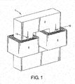
- Fig. 1 illustrates a top view of thermal well 10 installed in a transformer apparatus 1.
- the transformer apparatus 1 can be any suitable known transformer apparatus (e.g., single or three-phase transformers for power generation or distribution, motor drive applications, etc.
- the disclosed thermal well designs 10 can be employed in other situations or applications in which it is desirable to measure a temperature, including without limitation oil drilling, natural gas drilling, and the like).
- the transformer 1 includes a magnetic iron core structure 2, at least one primary coil 3 wound at least partially around the core structure 2, and at least one secondary coil 4 wound at least partially around the core structure 2.
- the transformer 1 can also include other necessary structures (not shown) and can be included in a machine our system (e.g., a motor drive with one or more power conversion stages and associated controllers, and the like).
- a thermal well 10 is positioned proximate one of the primary coil 3 and the secondary coil 4, or thermal wells 10 can be divided proximate each of the coils 3, 4.
- the thermal well 10 is positioned proximate the primary coil 3 and another thermal well 10 is located near the secondary coil 4.
- the thermal well 10 can be positioned between adjacent coils or windings of the primary coil 3 and/or of the secondary coil 4.
- a thermal well 10 can be positioned in any suitable position on, in or near the transformer 1 (e.g., on the primary coil 3, on the secondary coil 4, on the core structure 2, and the like), and any number of thermal wells 10 can be installed on or in various embodiments of a transformer apparatus 1 or other host system.
- the length of the thermal well assembly 10 is adjusted so that the tip of the thermal sensor 14 resides in the vertical center length of coil 3 or 4, since this is where the hottest temperature of the coil typically occurs.
- the thermal well 10 can include any suitable thermal sensor (e.g., a thermocouple, a thermal switch, a resistive temperature device (RTD, whether negative temperature coefficient NTC or positive temperature coefficient PTC), and the like).
- the thermal well 10 provides a signal representing the host system temperature or transition of such host system temperature passed a predetermined threshold, which in practice can be used by a control system to inhibit operation of the transformer apparatus 1 when the transformer apparatus 1 exceeds a temperature threshold.
- the disclosed thermal well 10 in certain embodiments has no air gaps, thereby preventing or inhibiting unwanted build-up of corona on the thermal well 10 and mitigating the possibility of such conditions proximate the primary and/or secondary coils 3 and 4.
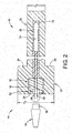
- Figs. 2-5 illustrate an example embodiment of the thermal well 10.
- the thermal well 10 includes a low relative dielectric constant structure 12, a thermal sensor 14, a first low relative dielectric constant potting material 16, and a second low relative dielectric constant potting material 18.
- the thermal well 10 in one embodiment has a generally round shape or outer profile in other embodiments (although any desired shape is possible, such as rectangular), where the round outer surface in certain embodiments advantageously conforms to or easily fils into a corresponding opening (not shown) between adjacent coils 3, 4 of the transformer apparatus 1. Conformance of the outer shape of the structure 12 to the host system advantageously increases the insulation thickness between the coil 3, 4 and the thermal sensor 14, thereby reducing the likelihood of arcing and/or corona formation.
- cylindrical or other outer structure profiles can be used, for example, to enhance cost-effective manufacturability of the structure 12 and the overall thermal well apparatus 10.
- the low relative dielectric constant structure 12 in certain embodiments can be made from any suitable non-chemically reactive material.
- the low relative dielectric constant structure 12 is made from Teflon that has a dielectric constant of approximately 2.1.
- the low relative dielectric constant structure 12 also is a continuous structure that does not have any air voids or pockets.
- making the structure 12 out of extruded or molded Teflon rod with this dielectric constant and which has a continuous structure (I) reduces or eliminates air void where corona can develop; (2) absorbs a larger voltage potential between the adjacent coils 3 or 4; (3) centers the thermal switch 14 between adjacent transformer coils in certain implementations thereby further reducing voltage stress levels; (4) provides good dielectric strength (5) is a good thermal conductor of heat from adjacent coil windings to the thermal sensor (6) has high temperature material characteristics @ 200 degree C so that it can be used in Underwriters Lab (UL) recognized 180 degree C insulation systems commonly used in transformer design and (7) provides a sealed thermal well enclosure reducing the chance of humidity, condensation and pollutants from degrading the assembly dielectric strength.
- UL Underwriters Lab
- Teflon advantageously provides for cost-effective manufacturing of a thermal well apparatus 10, whether by machining or other fabrication techniques.
- Other suitable low relative dielectric constant material 12 can be used, wherein the illustrated Teflon embodiments arc non-limiting.
- the low relative dielectric constant structure 12 can have any suitable dimensions. In one example, the structure 12 has a length of approximately 20.5" for housing a thermocouple or thermal switch in a gap between adjacent primary or secondary coils of a medium voltage or high-voltage transformer apparatus 1, although other dimensions can be used for a given end-use application.
- the low relative dielectric constant structure 12 has a rigid configuration for placement between the coils 3 and 4 and supporting the thermal sensor 14 and any include first potting material 16 and second potting material 18.
- the low relative dielectric constant structure 12 includes a first portion 20 and a second portion 22.
- the first portion 20 has a generally rectangular shape (although other shapes are possible, such as cylindrical) and a first outer dimension D 1 .
- the first portion 20 can have any suitable dimensions.
- the first portion 20 has a length of approximately 18.0" and an outer width of approximately 5/8" in the illustrated embodiment, where the width of the first portion 20 in a rectangular configuration can correspond to the first outer dimension D 1 .
- the second portion 22 in this embodiment also has a generally rectangular shape and a second outer dimension D 2 that is greater than the first outer dimension D 1 .
- the second portion 22 can have any suitable dimensions in various embodiments.
- the second portion 22 has a length of approximately 2.5" and a width of approximately 1.0".
- the width of the second portion 20 can correspond to the second outer dimension D 2 .
- the second portion 22 is positioned proximate the first portion 20 such that the low relative dielectric constant structure 12 has a substantially T-shaped configuration to provide at least one abutment surface 24 allowing the apparatus 10 to be easily installed with the first portion 20 disposed between adjacent transformer coils in the second portion 22 above the coils with the abutment surface(s) 24 resting on the upper ends of the coil for repeatable location of the enclosed thermal sensor 14 at a predetermined location between transformer coils 3, 4.
- the low relative dielectric constant structure 12 can have any suitable configuration, so long as the second portion 22 is positioned proximate the first portion 20.
- the abutment surfaces 24 are created by the second outer dimension D 2 being greater than the first outer dimension D 1 , although other abutments can be used even if the second portion 22 does not have a larger outer dimension than does the first portion 20.
- the abutment surfaces 24 allow the thermal well 10 to contact a portion of the transformer apparatus 1 (i.e., the primary or secondary coils 3 or 4) to be securely positioned on the transformer apparatus 1.
- the low relative dielectric constant structure 12 includes at least one internal cavity 26 configured to receive the thermocouple, thermal switch, RTD or other thermal sensor 14, and the cavity 26 also accommodates the first potting material 16, and the second potting material 18.
- the internal cavity 26 extends through the second portion 22 of the low relative dielectric constant structure 12 and into the first portion 20 thereof to any suitable depth to facilitate repeatable location of the thermal sensor 14 relative to the outlying transformer coils 3, 4.
- the internal cavity 26 in this non-limiting embodiment has a length of approximately 9.25" and a width of approximately 0.098". In one example, the length of internal cavity 26 is determined so that the thermal sensor 14 is approximately in the center of winding 3 and winding 4 in Fig.
- the internal cavity 26 in other embodiments can be offset relative to the axial center of the first and second portions 20 and 22.
- the internal cavity 26 includes an end region 28 located on the second portion 22 of the low relative dielectric constant structure 12. As shown in Fig. 2 , the end region 28 is spaced from the first portion 20; however, it will be appreciated that the end region 28 can extend into the first portion 20 in other embodiments in this example.
- the end region 28 has a length of approximately 1.25" and a width of approximately 0.196". In this regard, the end region 28 is twice as wide as the internal cavity 26, although not a strict requirement of all embodiments.
- the end region 28 includes at least one internal side wall 30 with optional threads 32 disposed on at least a portion thereof.
- the threads 32 in this embodiment are configured to engage a strain relief member 34 that includes corresponding complementary threads 36, as described in more detail below. In other implementations, the threads 32 can be omitted.
- Figs. 2-5 show the thermal sensor 14 inserted into a portion of the internal cavity 26.
- the thermal sensor 14 can be a thermocouple, such as a K type thermocouple, J type thermocouple, etc.
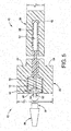
- a thermal switch sensor 14' can be used.
- the thermal sensor 14 can be an RTD (not shown). It will be appreciated that the thermal sensor 14 can be any suitable thermal sensor for monitoring the temperature of the transformer apparatus 1, and can provide a signal suitable for inhibiting operation of a host system by a controller (not shown) when the operating temperature exceeds a predefined threshold temperature.
- the thermal sensor 14 or 14' is at least partially located within the internal cavity 26, and may but need not be installed at or near the bottom of the cavity 26 for repeatable precise location relative to transformer coils of the host transformer apparatus 1. As shown in Figs. 2-5 , the thermal sensor 14 or 14' is disposed entirely within the internal cavity 26. As such, the thermal sensor 14 or 14' including the associated wires or leads 38 has a length of slightly less than 10.5" (with an external length of wires or leads 38 extending outward beyond this length from the apparatus 10). In some embodiments, the voltage potential of thermal sensor 14 in Fig, 2 or 14' in Fig.5 is usually at or near earth ground potential.
- a portion of the thermal sensor 14 or 14' can be disposed within the end region 28 or external to the low relative dielectric constant structure 12 in various alternate embodiments.
- the strain relief member 34 in certain embodiments is configured to engage a portion of the thermal sensor 14 or the leads 38 thereof to prevent or inhibit degradation of the wire leads 38 when the thermal well 10 is installed or removed from a host system 1.
- the thermal sensor 14 includes one or more wires 38 extending from a portion thereof to carry an analog signal (e.g., RTD or thermocouple) or a binary signal (e.g., thermal switch) to an external controller for evaluation of the transformer temperature.
- the wires 38 are operably electrically connected to such an external controller (not shown) using any suitable means.
- the wires 38 extend out of the end region 28 and through a portion of the strain relief member 34 such that the strain relief member 34 provides mechanical support for the wires 38.
- the threads 36 of the strain relief member 34 are threadedly engaged with the threads 32 of the end region 28.
- the strain relief member 34 is attached to the low relative dielectric constant structure 12 with a friction-fit (i.e., in a male-female connection).
- the use of threads 32 advantageously facilitates robust connection of the strain relief member 34 to a Teflon structure 12 which may have a low friction surface.
- a removable sleeve 40 e.g., a Varglass 240 size #10 sleeve, available from Skycraft Parts and Surplus, Winter Park, FL, not shown
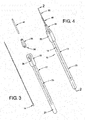
- the sleeve 40 is inserted through a portion of the strain gauge 36 and into the junction between the internal cavity 26 and the end region 28. In some instances, the sleeve can be removed.
- the wires 38 arc supported by the strain relief 34 to prevent separation of the wires 38 from the thermal sensor 14.
- the first potting material 16 is inserted into the internal cavity 26 following insertion of the thermal sensor 14, 14'.
- the first potting material 16 encapsulates at least a portion of the thermal sensor 14 within the internal cavity 26 in the illustrated embodiments.
- the first potting material 16 substantially fills the entire internal cavity 26, thereby completely surrounding the thermal switch 14 and mitigating or eliminating the existence of any air gaps within the cavity 26 in various embodiments.
- the first potting material 16 can be either epoxy (dielectric constant 3.5) or silicone gel into non-limiting examples, depending on the dielectric withstand voltage and corona inception voltage required for thermal well assembly 10 when mounted between transformer coil windings.
- the first potting material 16 is Sil-Gel 612 A/B (available from Wacker Chemical Corp., Canton, OH) that has a low dielectric constant of approximately 2.65.
- Sil-Gel potting material is preferred for higher voltage thermal well assemblies due to the fact that winding voltage stress divides as the inverse of a material's relative dielectric constant.
- the voltage that is on the high breakdown strength potting material increases as the voltage that is impressed on the air void with reduced chance of ionization corona discharge breakdown decreases in the air void.
- the first potting material 16 can be a solid or a liquid.
- the second potting material 18 in this example is inserted into the end region 28.
- the second potting material 18 in certain implementations fills at least a portion of the end region 28, and preferably eliminates or mitigates air gaps within the end region of the cavity 26. As shown in Figs. 2-5 , for example the second potting material 18 substantially fills the entire end region 28, thereby sealing the thermal sensor 14 within the internal cavity 26 along with the first potting material 16.
- the second potting material 18 in certain non-limiting embodiments can be either epoxy or silicone gel.
- the second potting material is Hard Epoxy #300/11 (available from Aeromarine Products, Inc., San Diego, CA) that has a dielectric constant of approximately 3.5, and the second potting material 18 can be a solid or a liquid.
- first and second potting materials 16 and 18 can be the same or different materials in various embodiments.
- the electric field is reduced in the end region 28 of the thermal well assembly 10, since the coil electric field is mostly confined in the air duct space between the copper coil windings.
- a hard epoxy with higher dielectric constant is acceptable to use if desired without fear of corona inception degradation.
- the first and second potting materials 16 and 18 prevent or inhibit air from entering the internal cavity 26 and the end region 28, thereby reducing the likelihood of arcing or corona formation within the thermal well 10.
- Fig. 6 shows another alternative embodiment of the thermal well 10'.
- the thermal well 10' is configured substantially identical to the thermal well 10, except as described below.
- the low relative dielectric constant structure 12 includes a second internal cavity 26' with a second end region 28' extending therefrom.
- a second thermal sensor 14' can be inserted into the second internal cavity 26'.
- the thermal well 10' can accommodate two different thermal sensors 14 (i.e., a thermocouple) and 14' (i.e., a thermal switch) or two identical thermal sensors 14 and 14' (e.g., two thermocouples, two thermal switches, two RTDs, and the like).
- first and second internal cavities 26 and 26' can have different sizes and dimensions to accommodate two different thermal switches (e.g., a thermocouple 14 in the first internal cavity 26 and a thermal switch 14' in the second internal cavity 26'), or the cavities 20, 26' can be similarly dimensioned in other embodiments.
- Fig. 7 shows a further alternative embodiment of a thermal well 10".
- the thermal well 10 includes a thermally conductive structure 12", a thermal switch 14", a low relative dielectric constant potting material 16", and a thermally insulating shroud 18".
- the thermally conductive structure 12" in Fig.7 includes a first portion 20" with a first outer dimension D 1 ' and a second portion 22" with a second outer dimension D 2 " that is greater than the first outer dimension D 1 ".
- the first portion 20" is adapted to fit between two or more transformer coils (i.e., the primary and secondary induction coils 3 and 4).
- the second portion 22" includes one or more abutment surfaces 24" that rest on a portion of the coils 3 and 4 when installed, thereby allowing the thermally conductive structure 12" to be securely positioned therebetween.
- the second portion 22" also includes at least one internal cavity 26" for accommodating at least one thermal switch 14 or 14'. It will be appreciated that the internal cavity 26" can additionally extend into a portion of the first portion 20".
- the internal cavity 26" includes an end region 28" with threads 32" for engagement with the strain relief member 34.
- a thermal switch 14 or 14' e.g., a thermocouple, a thermal switch, a resistant temperature device, and the like).
- the thermal switch 14 or 14' includes wires 38" extending out of the end region 28".
- the potting material 16" is inserted into the internal cavity 26 "to encapsulate at least a portion of the thermal sensor 14 or 14' within the internal cavity 26".
- the potting material 16" substantially fills the entire internal cavity 26", thereby completely surrounding the thermal switch 14 or 14".
- the thermally conductive structure 12" in this embodiment is made from a thermally conductive material (i.e., Glastic, CaolPoly D5506 Liquid Crystalline Polymer, CoolPoly D5108 Liquid Crystalline Polymer, and the like) to transfer heat generated by the coils 3 and 4 from the first portion 20" to the second portion 22". This allows heat to be drawn away from the coils 3, 4 and transfers the heat to the location of the thermal sensor 14 in this case.
- a thermally conductive material i.e., Glastic, CaolPoly D5506 Liquid Crystalline Polymer, CoolPoly D5108 Liquid Crystalline Polymer, and the like
- the thermal well 10" also includes a thermally insulating shroud 18" that surrounds at least a portion of the second portion 22".
- the shroud 18" allows for egress of the wires 38" out of the end region 28".
- the shroud 18" is configured to insulate heat loss to a local ambient (not shown) by any know method (e.g., convection, radiation, and the like).
- the method 100 includes forming a low relative dielectric constant structure 12 to include the first portion 20 and the second portion 22 (e.g., Step 102), as well as forming at least one internal cavity 26 within the end region 28 in the second portion 22 of the low relative dielectric constant structure 12 (Step 104).
- the method 100 further includes forming the threads 32 in the internal sidewall 30 of the end region 28 (e.g., Step 106), inserting the first low relative dielectric constant potting material 16 within at least a portion of the internal cavity 26 (e.g., Step 108) and inserting the thermal sensor 14 into the internal cavity 26 (e.g., Step 110).
- the method 100 includes inserting the second low relative dielectric constant potting material 18 within at least a portion of the end region 28 (e.g., Step 112), as well as engaging the thermal well 10 with the strain relief member 34 (e.g., Step 114) and inserting the thermal well 10 into a portion of the transformer apparatus 1 (e.g., Step 116).
- the low relative dielectric constant structure 12 is formed, in one embodiment to include a first portion 20 and a second portion 22, thereby providing the above-described abutment surface(s) 24.
- the low relative dielectric constant structure 12 can be formed by molding or machining (or any other suitable method).
- a single piece rectangular structure 12 can be formed by molding in certain embodiments, or a single piece structure 12 can be formed by machining, for example a cylindrical outer shape.
- the low relative dielectric constant structure 12 can have separate first and second portions 20 and 22 that are attached together in any suitable manner (e.g., welding, adhesives, mechanical fasteners, and the like).
- undesired portions of the low relative dielectric constant structure 12 can be removed in any suitable manner (e.g., sanding, cutting, and the like) to provide the low relative dielectric constant structure 12 with a substantially T-shaped configuration or other suitable shape, for example, including one or more abutment surfaces 24.
- the first and second portions 20 and 22 are formed in one example at 102 in Fig.8 so that the first portion 20 has a first outer dimension D 1 and the second portion 22 has a second outer dimension D 2 that is greater than the first outer dimension D 1 (e.g., Figs. 2 and 3 above)
- the abutment surfaces 24 are consequently formed on the second portion 22 in the illustrated embodiments.
- the abutment surfaces 24 extend at least partially outwardly from the second portion 22.
- At Step 104 in Fig. 8 at least one internal cavity 26 with the end region 28 is formed in the second portion 22.
- the internal cavity 26 can be formed in any suitable manner (e.g., drilling, cutting, sand-blasting, molding, machining, and the like).
- the internal cavity 26 is sized and dimensioned during formation at 104 so as to receive the thermal switch 14, the first potting material 16, and the second potting material 18.
- the internal cavity 26, moreover, is formed at 104 to extend through the second portion 22 and into the first portion 20 thereof.
- the internal cavity 26 can extend into only the second portion 22 in other embodiments, or through the entire first portion 20.
- the internal cavity 26 is centered on the low relative dielectric constant structure 12 during formation at 104, thereby advantageously reducing voltage stress levels on an installed sensor 14, 14'.
- the formed internal cavity 26 can be off-centered on the low relative dielectric constant structure 12.
- the interior dimensions of the end region 28 can be formed at 104 so as to be larger than the internal cavity 26.
- threads 32 are optionally formed in the internal sidewall 30 of the end region 28.
- the threads 32 can be formed in any suitable manner (e.g., tapping, and the like).
- the threads 32 are disposed on only a portion of the end region 28.
- the threads 32 are disposed on the entire length of the end region 28. It will be appreciated that the threads 32 can be formed in any other suitable location within the end region 28 (e.g., on a bottom surface, on another sidewall, and the like), or that the threads 32 can be formed on any suitable portion of the low relative dielectric constant structure 12 to engage any included strain relief member 34.
- the first low relative dielectric constant potting material 16 is inserted within at least a portion of the internal cavity 26.
- the first potting material 16 can be inserted by any suitable method (e.g., pouring, packing, applied with a caulk-like gun, delivered with a balloon-type device, and the like).
- the first potting material 16 is a liquid which is cured after the thermal sensor 14 is inserted into the internal cavity 26.
- a portion of the internal cavity 26 is filled with the first potting material 16 before insertion of the thermal sensor 14 (e.g., at 110 in Fig. 6 ).
- the entire internal cavity 26 is substantially filled with first potting material 16 for the thermal sensor 14 is installed.
- the thermal sensor 14 is inserted into the cavity 26 before insertion of the first potting material.
- the internal cavity 26 is substantially entirely filled in certain advantageous implementations with the first potting material 16 so that the thermal switch, thermocouple, RTD 14 is encapsulated thereby while mitigating or avoiding any air gaps within the cavity 26.
- the first potting material 16 is only disposed within the internal cavity 26.
- the first potting material 16 can be disposed within all or at least a portion of the end region 28 as well and other embodiments.
- the first potting material 16 inserted at 108 can be either epoxy or silicone gel into non-limiting examples.
- the first potting material 16 is Sil-Gel 612 A/B that has a dielectric constant of approximately 2.65.
- parts A and B of a Sil-Gel 612 product (available from Wacker Chemical Corp., Canton, OH) are mixed together and inserted into the cavity 26 at 108 to provide the first potting material 16.
- the thermal sensor 14 is inserted into the internal cavity 26.
- the thermal sensor 14 is entirely disposed within the internal cavity 26, with one or more lead wires 38 thereof extending outward of the thermal well cavity 26.
- the thermal sensor 14 is disposed in portions of both the internal cavity 26 and the end region 28.
- a portion of the thermal sensor 14 extends out of the thermal well 10 from the end region 28.
- the thermal switch 14 in certain implementations is inserted at 110 into the internal cavity 26 until it reaches a bottom of the internal cavity 26 so as to provide repeatable location of the sensor 14 with respect to outlying transformer coils in use in a host system 1.
- the thermal switch 14 can be wrapped in an insulator (e.g., Teflon tape, etc.). Excess first potting material 16 spills out of the internal cavity 26 during insertion of the thermal sensor 14 therein at 110 in certain implementations. At 110, moreover, the first potting material 16 may be cured and cooled in certain embodiments.
- the sensor wires 38 extend out of the internal cavity 26 for later connection with a controller (not shown) of the transformer apparatus 1 or other host system. After the thermal sensor 14 is inserted first potting material 16 is poured into the internal cavity 26, air voids and bubbles therein are eliminated through a vacuum process.
- the second low relative dielectric constant potting material 18 is inserted within at least a portion of the end region 28.
- the second potting material 18 can be inserted by any suitable method at 112 (e.g., pouring, packing, applied with a caulk-like gun, delivered with a balloon-type device, and the like).
- the second potting material 18 in one embodiment is a liquid; however, the material 18 can be a solid in other implementations.
- a portion of the end region 28 is filled with the second potting material 18.
- the entire end region 28 is substantially filled with second potting material 18.
- the end region 28 is filled with the second potting material 18 so that the internal cavity 26 is scaled.
- the second potting material 18 is only disposed within the end region 28, although the second potting material 18 can be disposed within the internal cavity 26 in other embodiments.
- suitable second potting material 18 include epoxy and silicone gel.
- the second potting material is Aeromarine Epoxy #300/11 with a dielectric constant of approximately 3.5, where Hard Epoxy #300/11 (e.g., available from Aeromarine Products, Inc., San Diego, CA) are mixed together to provide the second potting material 18.
- the sleeve 40 is inserted into the junction between the internal cavity 26 and the end region 28 to act as a stop therebetween. The second potting material 18 is then poured into the end region 28. The sleeve 40 may then be removed. The thermal well 10 can be left to cure.
- the first and second potting materials 16 and 18 can be the same or different materials in various embodiments.
- the thermal well 10 is optionally engaged with any included strain relief member 34.
- the strain relief member 34 includes threads 36 that are complementary to the threads 32 of the thermal well 10, and the strain relief member 34 is threadedly engaged with the thermal well 10 at the end region 28 of the low relative dielectric constant structure 12 at 114.
- the strain relief member 34 is attached to the low relative dielectric constant structure 12 at 114 via a friction-fit (e.g., in a male-female connection).
- the wires 38 of the thermal sensor 14 Prior to engagement of the strain relief member 34 and the thermal well 10, the wires 38 of the thermal sensor 14 are fed through a channel (not shown) of the strain relief member 34, thereby preventing separation of the wires 38 from the thermal sensor and providing mechanical support for the wires 38.
- the thermal well 10 is inserted into a portion of the transformer apparatus 1.
- the thermal well 10 is rectangular, and inserted into a rectangular opening on the transformer apparatus 1, for example, between adjacent primary windings 3 or between adjacent secondary windings 4.
- the thermal well 10 (and the corresponding opening in a given host system) can have any shape.
- the thermal well 10 can be positioned in any suitable position on the transformer apparatus 1 or other host system (e.g., proximate a primary coil 3, proximate a secondary coil 4, proximate the core structure 2, etc.).
Landscapes
- Physics & Mathematics (AREA)
- General Physics & Mathematics (AREA)
- Engineering & Computer Science (AREA)
- Power Engineering (AREA)
- Measuring Temperature Or Quantity Of Heat (AREA)
- Housings And Mounting Of Transformers (AREA)
Abstract
Description
- The instant application claims priority to
U.S. Provisional Application Serial No. 62/048,436, filed September 10, 2014 - The subject matter disclosed herein relates to temperature monitoring, and more specifically to temperature monitoring in transformers, especially those containing high voltage windings.
- Various aspects of the present disclosure are now summarized to facilitate a basic understanding of the disclosure, wherein this summary is not an extensive overview of the disclosure, and is intended neither to identify certain elements of the disclosure, nor to delineate the scope thereof. Rather, the primary purpose of this summary is to present various concepts of the disclosure in a simplified form prior to the more detailed description that is presented hereinafter. The present disclosure provides a thermal well with a thermal sensor within a cavity of a low dielectric constant structure that monitors a temperature of an apparatus (for example, one or more coils of a transformer apparatus) and provides a signal that can be used to inhibit operation of the apparatus when the temperature thereof exceeds a pre-defined threshold temperature. In further aspects, the thermal well includes one or more potting layers to remove air voids within the thermal well assembly, thereby reducing the amount of corona build-up thereon. Even minute air voids will reduce the overall dielectric withstand voltage of the entire assembly due to the air voids becoming voltage stress concentrators and exceeding the corona inception voltage of air according to Paschen's law. Continuous operation with corona discharges in the air void can lead to insulation erosion and eventual voltage breakdown well before expected insulation end of life.
- The following description and drawings set forth certain illustrative implementations of the disclosure in detail, which are indicative of several exemplary ways in which the various principles of the disclosure may be carried out. The illustrated examples, however, are not exhaustive of the many possible embodiments of the disclosure. Other objects, advantages and novel features of the disclosure will be set forth in the following detailed description when considered in conjunction with the drawings, in which:
-
Fig. 1 is a perspective view of the thermal well assembly mounted between transformer coils; -
Fig. 2 is a sectional side elevation view taken along Line 2-2 inFig. 4 ; -
Fig. 3 is a disassembled view of the thermal well; -
Fig. 4 is an assembled view of the thermal well; -
Fig. 5 is a sectional side elevation view of one thermal well implementation; -
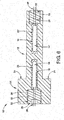
Fig. 6 is a sectional side elevation view of the thermal well implemented with dual temperature sensors; -
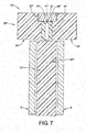
Fig. 7 is a sectional side elevation view of an alternate thermal well implementation mounted between transformer coil wings; and -
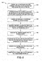
Fig. 8 is a flow diagram of the thermal well assembly. - Various embodiments are hereinafter illustrated and described, wherein the disclosure is not limited to the specific examples shown and described. A temperature monitoring apparatus or thermal well and methods arc presented in which a thermal well includes a thermal sensor and one or more low relative dielectric constant potting layers within a low relative dielectric constant structure to mitigate or avoid air gaps in the thermal well. The low dielectric constant structure and potting layers in certain embodiments advantageously mitigate the potential for arcing and build-up of undesirable corona once positioned between high potential transformer coils or windings or in other high voltage or explosive environments.
- Transformers are used for power generation and distribution, often for high energy applications (e.g., oil drilling, natural gas drilling, electricity generation, motor drives, and the like). In use, the transformer primary and secondary coils conduct current and are often at high voltage potentials, and the transformer core and/or windings typically heat up in operation due to current conduction. Moreover, undesirable currents in excess of expected design levels can cause the transformer coil temperatures to rise significantly. In order to monitor the status of the transformer and any downstream equipment with respect to over current conditions or other operational degradation, a thermal well or thermal sensor probe can be installed between adjacent transformer coils provide a signal representing the temperature of the transformer. In practice, knowing the transformer temperature can facilitate proactive identification of potential thermal stress or other component degradation in an electrical system. Some thermal probes use an insulating material (such as tape or a gel) or rolled multiple layers of an insulating material disposed between the thermal sensor and the coils, for example with a tape wrapped around a thermocouple. In use, the thermal well signal can be provided to a control system to monitor the temperature of the coils, and the sensed transformer temperature can be compared with a threshold temperature with the system selectively performing one or more remedial actions if the sensed operating temperature exceeds the threshold. A thermal switch may be used in the sensor probe, providing a signal state change upon the temperature reaching a predetermined level, with a connected controller performing a selected action in response (e.g., shut down, generate an alarm, and the like).
- When the thermal well is positioned between the coils, pockets of air are often formed therebetween and/or between adjacent layers of wrapped insulation tape or rolled insulating layers. A high voltage potential between a transformer coil and a thermocouple or other thermal sensor, however, can make the thermal well susceptible to arcing conditions and corona build-up between the thermal well and the coils. Such arcing and corona can lead to degradation of insulating layers or failure of the thermal sensor, and further temperature monitoring would require repair or replacement which can be costly and labor-intensive in certain applications.
- Referring initially to
Figs. 1-5 , the present disclosure accordingly providesthermal well apparatus 10 which employs a low dielectricconstant material structure 12 to house athermal sensor 14 and thus inhibit arcing and/or corona conditions, and various embodiments further mitigate the presence of air between the thermal sensor and an outside surface of a thermal well by potting the cavity housing the thermal sensor using low relative dielectricconstant potting material -
Fig. 1 illustrates a top view ofthermal well 10 installed in a transformer apparatus 1. The transformer apparatus 1 can be any suitable known transformer apparatus (e.g., single or three-phase transformers for power generation or distribution, motor drive applications, etc. Moreover, the disclosedthermal well designs 10 can be employed in other situations or applications in which it is desirable to measure a temperature, including without limitation oil drilling, natural gas drilling, and the like). In the example ofFig. 1 , the transformer 1 includes a magneticiron core structure 2, at least oneprimary coil 3 wound at least partially around thecore structure 2, and at least onesecondary coil 4 wound at least partially around thecore structure 2. The transformer 1 can also include other necessary structures (not shown) and can be included in a machine our system (e.g., a motor drive with one or more power conversion stages and associated controllers, and the like). In some instances, athermal well 10 is positioned proximate one of theprimary coil 3 and thesecondary coil 4, orthermal wells 10 can be divided proximate each of thecoils Fig. 1 , thethermal well 10 is positioned proximate theprimary coil 3 and anotherthermal well 10 is located near thesecondary coil 4. In addition, in certain applications, thethermal well 10 can be positioned between adjacent coils or windings of theprimary coil 3 and/or of thesecondary coil 4. In this regard, athermal well 10 can be positioned in any suitable position on, in or near the transformer 1 (e.g., on theprimary coil 3, on thesecondary coil 4, on thecore structure 2, and the like), and any number ofthermal wells 10 can be installed on or in various embodiments of a transformer apparatus 1 or other host system. In one example, the length of thethermal well assembly 10 is adjusted so that the tip of thethermal sensor 14 resides in the vertical center length ofcoil - The
thermal well 10, moreover, can include any suitable thermal sensor (e.g., a thermocouple, a thermal switch, a resistive temperature device (RTD, whether negative temperature coefficient NTC or positive temperature coefficient PTC), and the like). Advantageously, thethermal well 10 provides a signal representing the host system temperature or transition of such host system temperature passed a predetermined threshold, which in practice can be used by a control system to inhibit operation of the transformer apparatus 1 when the transformer apparatus 1 exceeds a temperature threshold. Advantageously, the disclosedthermal well 10 in certain embodiments has no air gaps, thereby preventing or inhibiting unwanted build-up of corona on thethermal well 10 and mitigating the possibility of such conditions proximate the primary and/orsecondary coils -
Figs. 2-5 illustrate an example embodiment of thethermal well 10. As shown inFigs. 2-5 , thethermal well 10 includes a low relative dielectricconstant structure 12, athermal sensor 14, a first low relative dielectricconstant potting material 16, and a second low relative dielectricconstant potting material 18. Thethermal well 10 in one embodiment has a generally round shape or outer profile in other embodiments (although any desired shape is possible, such as rectangular), where the round outer surface in certain embodiments advantageously conforms to or easily fils into a corresponding opening (not shown) betweenadjacent coils structure 12 to the host system advantageously increases the insulation thickness between thecoil thermal sensor 14, thereby reducing the likelihood of arcing and/or corona formation. In other embodiments, cylindrical or other outer structure profiles can be used, for example, to enhance cost-effective manufacturability of thestructure 12 and the overallthermal well apparatus 10. - The low relative dielectric
constant structure 12 in certain embodiments can be made from any suitable non-chemically reactive material. In some examples, the low relative dielectricconstant structure 12 is made from Teflon that has a dielectric constant of approximately 2.1. The low relative dielectricconstant structure 12 also is a continuous structure that does not have any air voids or pockets. Advantageously, in some examples, making thestructure 12 out of extruded or molded Teflon rod with this dielectric constant and which has a continuous structure: (I) reduces or eliminates air void where corona can develop; (2) absorbs a larger voltage potential between theadjacent coils thermal switch 14 between adjacent transformer coils in certain implementations thereby further reducing voltage stress levels; (4) provides good dielectric strength (5) is a good thermal conductor of heat from adjacent coil windings to the thermal sensor (6) has high temperature material characteristics @ 200 degree C so that it can be used in Underwriters Lab (UL) recognized 180 degree C insulation systems commonly used in transformer design and (7) provides a sealed thermal well enclosure reducing the chance of humidity, condensation and pollutants from degrading the assembly dielectric strength. Moreover, Teflon advantageously provides for cost-effective manufacturing of athermal well apparatus 10, whether by machining or other fabrication techniques. Other suitable low relative dielectricconstant material 12 can be used, wherein the illustrated Teflon embodiments arc non-limiting. The low relative dielectricconstant structure 12 can have any suitable dimensions. In one example, thestructure 12 has a length of approximately 20.5" for housing a thermocouple or thermal switch in a gap between adjacent primary or secondary coils of a medium voltage or high-voltage transformer apparatus 1, although other dimensions can be used for a given end-use application. The low relative dielectricconstant structure 12 has a rigid configuration for placement between thecoils thermal sensor 14 and any includefirst potting material 16 andsecond potting material 18. - As shown in the embodiment of
Figs. 2-5 , the low relative dielectricconstant structure 12 includes afirst portion 20 and asecond portion 22. Thefirst portion 20 has a generally rectangular shape (although other shapes are possible, such as cylindrical) and a first outer dimension D1. Thefirst portion 20 can have any suitable dimensions. For example, thefirst portion 20 has a length of approximately 18.0" and an outer width of approximately 5/8" in the illustrated embodiment, where the width of thefirst portion 20 in a rectangular configuration can correspond to the first outer dimension D1. Thesecond portion 22 in this embodiment also has a generally rectangular shape and a second outer dimension D2 that is greater than the first outer dimension D1. Thesecond portion 22 can have any suitable dimensions in various embodiments. In the illustrated example, thesecond portion 22 has a length of approximately 2.5" and a width of approximately 1.0". For example, the width of thesecond portion 20 can correspond to the second outer dimension D2. Thesecond portion 22 is positioned proximate thefirst portion 20 such that the low relative dielectricconstant structure 12 has a substantially T-shaped configuration to provide at least oneabutment surface 24 allowing theapparatus 10 to be easily installed with thefirst portion 20 disposed between adjacent transformer coils in thesecond portion 22 above the coils with the abutment surface(s) 24 resting on the upper ends of the coil for repeatable location of the enclosedthermal sensor 14 at a predetermined location betweentransformer coils constant structure 12 can have any suitable configuration, so long as thesecond portion 22 is positioned proximate thefirst portion 20. In this embodiment, the abutment surfaces 24 are created by the second outer dimension D2 being greater than the first outer dimension D1, although other abutments can be used even if thesecond portion 22 does not have a larger outer dimension than does thefirst portion 20. Advantageously, the abutment surfaces 24 allow the thermal well 10 to contact a portion of the transformer apparatus 1 (i.e., the primary orsecondary coils 3 or 4) to be securely positioned on the transformer apparatus 1. - In some instances, the low relative dielectric
constant structure 12 includes at least oneinternal cavity 26 configured to receive the thermocouple, thermal switch, RTD or otherthermal sensor 14, and thecavity 26 also accommodates thefirst potting material 16, and thesecond potting material 18. As shown inFigs. 2 and3 , theinternal cavity 26 extends through thesecond portion 22 of the low relative dielectricconstant structure 12 and into thefirst portion 20 thereof to any suitable depth to facilitate repeatable location of thethermal sensor 14 relative to the outlying transformer coils 3, 4. Theinternal cavity 26 in this non-limiting embodiment has a length of approximately 9.25" and a width of approximately 0.098". In one example, the length ofinternal cavity 26 is determined so that thethermal sensor 14 is approximately in the center of winding 3 and winding 4 in Fig. for the most accurate hot spot coil temperature measurement. Theinternal cavity 26, moreover, advantageously is centered on the first andsecond portions thermal sensor 14 in the gap betweenadjacent transformer coils sensor 14 in use. However, it will be appreciated that theinternal cavity 26 in other embodiments can be offset relative to the axial center of the first andsecond portions - The
internal cavity 26 includes anend region 28 located on thesecond portion 22 of the low relative dielectricconstant structure 12. As shown inFig. 2 , theend region 28 is spaced from thefirst portion 20; however, it will be appreciated that theend region 28 can extend into thefirst portion 20 in other embodiments in this example. Theend region 28 has a length of approximately 1.25" and a width of approximately 0.196". In this regard, theend region 28 is twice as wide as theinternal cavity 26, although not a strict requirement of all embodiments. In some examples, theend region 28 includes at least oneinternal side wall 30 withoptional threads 32 disposed on at least a portion thereof. Thethreads 32 in this embodiment are configured to engage astrain relief member 34 that includes correspondingcomplementary threads 36, as described in more detail below. In other implementations, thethreads 32 can be omitted. -
Figs. 2-5 show thethermal sensor 14 inserted into a portion of theinternal cavity 26. In one example, as shown inFigs. 2-4 , thethermal sensor 14 can be a thermocouple, such as a K type thermocouple, J type thermocouple, etc. In another example, as shown inFig. 5 , a thermal switch sensor 14' can be used. In a further example, thethermal sensor 14 can be an RTD (not shown). It will be appreciated that thethermal sensor 14 can be any suitable thermal sensor for monitoring the temperature of the transformer apparatus 1, and can provide a signal suitable for inhibiting operation of a host system by a controller (not shown) when the operating temperature exceeds a predefined threshold temperature. Thethermal sensor 14 or 14' is at least partially located within theinternal cavity 26, and may but need not be installed at or near the bottom of thecavity 26 for repeatable precise location relative to transformer coils of the host transformer apparatus 1. As shown inFigs. 2-5 , thethermal sensor 14 or 14' is disposed entirely within theinternal cavity 26. As such, thethermal sensor 14 or 14' including the associated wires or leads 38 has a length of slightly less than 10.5" (with an external length of wires or leads 38 extending outward beyond this length from the apparatus 10). In some embodiments, the voltage potential ofthermal sensor 14 inFig, 2 or 14' inFig.5 is usually at or near earth ground potential. For example, the purpose of maintaining a large distance from the tip ofthermal sensor 14 or 14' to the end of the low relative dielectricconstant structure 12 rod is to reduce the corona inception voltage stress in the air (for example, with a dielectric constant =1.0) below and external toassembly 10 due to electric field gradient stress at the dielectric constant discontinuity. However, it will be appreciated that a portion of thethermal sensor 14 or 14' can be disposed within theend region 28 or external to the low relative dielectricconstant structure 12 in various alternate embodiments. - The
strain relief member 34 in certain embodiments is configured to engage a portion of thethermal sensor 14 or theleads 38 thereof to prevent or inhibit degradation of the wire leads 38 when thethermal well 10 is installed or removed from a host system 1. For example, thethermal sensor 14 includes one ormore wires 38 extending from a portion thereof to carry an analog signal (e.g., RTD or thermocouple) or a binary signal (e.g., thermal switch) to an external controller for evaluation of the transformer temperature. In practice, thewires 38 are operably electrically connected to such an external controller (not shown) using any suitable means. In addition, thewires 38 extend out of theend region 28 and through a portion of thestrain relief member 34 such that thestrain relief member 34 provides mechanical support for thewires 38. In one example, thethreads 36 of thestrain relief member 34 are threadedly engaged with thethreads 32 of theend region 28. In another example, thestrain relief member 34 is attached to the low relative dielectricconstant structure 12 with a friction-fit (i.e., in a male-female connection). In this regard, the use ofthreads 32 advantageously facilitates robust connection of thestrain relief member 34 to aTeflon structure 12 which may have a low friction surface. In some examples, a removable sleeve 40 (e.g., a Varglass 240size # 10 sleeve, available from Skycraft Parts and Surplus, Winter Park, FL, not shown) is inserted into the junction between theinternal cavity 26 and theend region 28 to act as a stop therebetween. As shown inFigs. 3 and 4 , thesleeve 40 is inserted through a portion of thestrain gauge 36 and into the junction between theinternal cavity 26 and theend region 28. In some instances, the sleeve can be removed. Advantageously, thewires 38 arc supported by thestrain relief 34 to prevent separation of thewires 38 from thethermal sensor 14. - In this embodiment, moreover, the
first potting material 16 is inserted into theinternal cavity 26 following insertion of thethermal sensor 14, 14'. For example, thefirst potting material 16 encapsulates at least a portion of thethermal sensor 14 within theinternal cavity 26 in the illustrated embodiments. As shown inFigs. 2-5 , thefirst potting material 16 substantially fills the entireinternal cavity 26, thereby completely surrounding thethermal switch 14 and mitigating or eliminating the existence of any air gaps within thecavity 26 in various embodiments. Thefirst potting material 16 can be either epoxy (dielectric constant 3.5) or silicone gel into non-limiting examples, depending on the dielectric withstand voltage and corona inception voltage required forthermal well assembly 10 when mounted between transformer coil windings. In some embodiments, thefirst potting material 16 is Sil-Gel 612 A/B (available from Wacker Chemical Corp., Canton, OH) that has a low dielectric constant of approximately 2.65. For example, Sil-Gel potting material is preferred for higher voltage thermal well assemblies due to the fact that winding voltage stress divides as the inverse of a material's relative dielectric constant. Thus, potting material with lower dielectric constants closer to that of an air void with dielectric constant =1.0 are preferred. As a result, the voltage that is on the high breakdown strength potting material increases as the voltage that is impressed on the air void with reduced chance of ionization corona discharge breakdown decreases in the air void. It will be appreciated that thefirst potting material 16 can be a solid or a liquid. - The
second potting material 18 in this example is inserted into theend region 28. Thesecond potting material 18 in certain implementations fills at least a portion of theend region 28, and preferably eliminates or mitigates air gaps within the end region of thecavity 26. As shown inFigs. 2-5 , for example thesecond potting material 18 substantially fills theentire end region 28, thereby sealing thethermal sensor 14 within theinternal cavity 26 along with thefirst potting material 16. Thesecond potting material 18 in certain non-limiting embodiments can be either epoxy or silicone gel. In one example, the second potting material is Hard Epoxy #300/11 (available from Aeromarine Products, Inc., San Diego, CA) that has a dielectric constant of approximately 3.5, and thesecond potting material 18 can be a solid or a liquid. It will also be appreciated that the first andsecond potting materials end region 28 of thethermal well assembly 10, since the coil electric field is mostly confined in the air duct space between the copper coil windings. A hard epoxy with higher dielectric constant is acceptable to use if desired without fear of corona inception degradation. Advantageously, the first andsecond potting materials internal cavity 26 and theend region 28, thereby reducing the likelihood of arcing or corona formation within thethermal well 10. -
Fig. 6 shows another alternative embodiment of the thermal well 10'. The thermal well 10' is configured substantially identical to thethermal well 10, except as described below. In this embodiment, the low relative dielectricconstant structure 12 includes a second internal cavity 26' with a second end region 28' extending therefrom. A second thermal sensor 14' can be inserted into the second internal cavity 26'. In some examples, the thermal well 10' can accommodate two different thermal sensors 14 (i.e., a thermocouple) and 14' (i.e., a thermal switch) or two identicalthermal sensors 14 and 14' (e.g., two thermocouples, two thermal switches, two RTDs, and the like). In addition, the first and secondinternal cavities 26 and 26' can have different sizes and dimensions to accommodate two different thermal switches (e.g., athermocouple 14 in the firstinternal cavity 26 and a thermal switch 14' in the second internal cavity 26'), or thecavities 20, 26' can be similarly dimensioned in other embodiments. -
Fig. 7 shows a further alternative embodiment of athermal well 10". In this embodiment, the thermal well 10" includes a thermallyconductive structure 12", athermal switch 14", a low relative dielectricconstant potting material 16", and a thermally insulatingshroud 18". Similar to the low relative dielectricconstant structure 12 described above, the thermallyconductive structure 12" inFig.7 includes afirst portion 20" with a first outer dimension D1' and asecond portion 22" with a second outer dimension D2" that is greater than the first outer dimension D1". Thefirst portion 20" is adapted to fit between two or more transformer coils (i.e., the primary andsecondary induction coils 3 and 4). Thesecond portion 22" includes one or more abutment surfaces 24" that rest on a portion of thecoils conductive structure 12" to be securely positioned therebetween. Thesecond portion 22" also includes at least oneinternal cavity 26" for accommodating at least onethermal switch 14 or 14'. It will be appreciated that theinternal cavity 26" can additionally extend into a portion of thefirst portion 20". Theinternal cavity 26" includes anend region 28" withthreads 32" for engagement with thestrain relief member 34. Athermal switch 14 or 14' (e.g., a thermocouple, a thermal switch, a resistant temperature device, and the like). Thethermal switch 14 or 14' includeswires 38" extending out of theend region 28". The pottingmaterial 16" is inserted into theinternal cavity 26 "to encapsulate at least a portion of thethermal sensor 14 or 14' within theinternal cavity 26". The pottingmaterial 16" substantially fills the entireinternal cavity 26", thereby completely surrounding thethermal switch - The thermally
conductive structure 12" in this embodiment is made from a thermally conductive material (i.e., Glastic, CaolPoly D5506 Liquid Crystalline Polymer, CoolPoly D5108 Liquid Crystalline Polymer, and the like) to transfer heat generated by thecoils first portion 20" to thesecond portion 22". This allows heat to be drawn away from thecoils thermal sensor 14 in this case. - The thermal well 10" also includes a thermally insulating
shroud 18" that surrounds at least a portion of thesecond portion 22". Theshroud 18" allows for egress of thewires 38" out of theend region 28". Theshroud 18" is configured to insulate heat loss to a local ambient (not shown) by any know method (e.g., convection, radiation, and the like). - Referring now to
Fig. 8 an example process ormethod 100 is described for making a thermal well, such as the thermal well 10 described above. Although themethod 100 is described in terms of thethermal well 10, it will be appreciated that themethod 100 can be used to make the thermal well 10' or the thermal well 10" or other thermal wells (not shown). Themethod 100 includes forming a low relative dielectricconstant structure 12 to include thefirst portion 20 and the second portion 22 (e.g., Step 102), as well as forming at least oneinternal cavity 26 within theend region 28 in thesecond portion 22 of the low relative dielectric constant structure 12 (Step 104). Themethod 100 further includes forming thethreads 32 in theinternal sidewall 30 of the end region 28 (e.g., Step 106), inserting the first low relative dielectricconstant potting material 16 within at least a portion of the internal cavity 26 (e.g., Step 108) and inserting thethermal sensor 14 into the internal cavity 26 (e.g., Step 110). In addition, themethod 100 includes inserting the second low relative dielectricconstant potting material 18 within at least a portion of the end region 28 (e.g., Step 112), as well as engaging the thermal well 10 with the strain relief member 34 (e.g., Step 114) and inserting the thermal well 10 into a portion of the transformer apparatus 1 (e.g., Step 116). - At
Step 102, the low relative dielectricconstant structure 12 is formed, in one embodiment to include afirst portion 20 and asecond portion 22, thereby providing the above-described abutment surface(s) 24. The low relative dielectricconstant structure 12 can be formed by molding or machining (or any other suitable method). For example, a single piecerectangular structure 12 can be formed by molding in certain embodiments, or asingle piece structure 12 can be formed by machining, for example a cylindrical outer shape. In another non-limiting example, the low relative dielectricconstant structure 12 can have separate first andsecond portions constant structure 12 can be removed in any suitable manner (e.g., sanding, cutting, and the like) to provide the low relative dielectricconstant structure 12 with a substantially T-shaped configuration or other suitable shape, for example, including one or more abutment surfaces 24. The first andsecond portions Fig.8 so that thefirst portion 20 has a first outer dimension D1 and thesecond portion 22 has a second outer dimension D2 that is greater than the first outer dimension D1 (e.g.,Figs. 2 and3 above) Upon formation of the first andsecond portions second portion 22 in the illustrated embodiments. In one example, the abutment surfaces 24 extend at least partially outwardly from thesecond portion 22. - At
Step 104 inFig. 8 , at least oneinternal cavity 26 with theend region 28 is formed in thesecond portion 22. Theinternal cavity 26 can be formed in any suitable manner (e.g., drilling, cutting, sand-blasting, molding, machining, and the like). Theinternal cavity 26 is sized and dimensioned during formation at 104 so as to receive thethermal switch 14, thefirst potting material 16, and thesecond potting material 18. Theinternal cavity 26, moreover, is formed at 104 to extend through thesecond portion 22 and into thefirst portion 20 thereof. However, it will be appreciated that theinternal cavity 26 can extend into only thesecond portion 22 in other embodiments, or through the entirefirst portion 20. In some examples, theinternal cavity 26 is centered on the low relative dielectricconstant structure 12 during formation at 104, thereby advantageously reducing voltage stress levels on an installedsensor 14, 14'. In other examples, the formedinternal cavity 26 can be off-centered on the low relative dielectricconstant structure 12. In some instances, the interior dimensions of theend region 28 can be formed at 104 so as to be larger than theinternal cavity 26. - At 106 in
Fig. 8 ,threads 32 are optionally formed in theinternal sidewall 30 of theend region 28. Thethreads 32, if used, can be formed in any suitable manner (e.g., tapping, and the like). In some examples, thethreads 32 are disposed on only a portion of theend region 28. In other examples, thethreads 32 are disposed on the entire length of theend region 28. It will be appreciated that thethreads 32 can be formed in any other suitable location within the end region 28 (e.g., on a bottom surface, on another sidewall, and the like), or that thethreads 32 can be formed on any suitable portion of the low relative dielectricconstant structure 12 to engage any includedstrain relief member 34. - At
Step 108, the first low relative dielectricconstant potting material 16 is inserted within at least a portion of theinternal cavity 26. Thefirst potting material 16 can be inserted by any suitable method (e.g., pouring, packing, applied with a caulk-like gun, delivered with a balloon-type device, and the like). Thefirst potting material 16 is a liquid which is cured after thethermal sensor 14 is inserted into theinternal cavity 26. In some examples, a portion of theinternal cavity 26 is filled with thefirst potting material 16 before insertion of the thermal sensor 14 (e.g., at 110 inFig. 6 ). In other examples, the entireinternal cavity 26 is substantially filled withfirst potting material 16 for thethermal sensor 14 is installed. In other possible implementations, thethermal sensor 14 is inserted into thecavity 26 before insertion of the first potting material. It will be appreciated that theinternal cavity 26 is substantially entirely filled in certain advantageous implementations with thefirst potting material 16 so that the thermal switch, thermocouple,RTD 14 is encapsulated thereby while mitigating or avoiding any air gaps within thecavity 26. In some instances, thefirst potting material 16 is only disposed within theinternal cavity 26. However, it will be appreciated that thefirst potting material 16 can be disposed within all or at least a portion of theend region 28 as well and other embodiments. Thefirst potting material 16 inserted at 108 can be either epoxy or silicone gel into non-limiting examples. In one example, thefirst potting material 16 is Sil-Gel 612 A/B that has a dielectric constant of approximately 2.65. In this example, parts A and B of a Sil-Gel 612 product (available from Wacker Chemical Corp., Canton, OH) are mixed together and inserted into thecavity 26 at 108 to provide thefirst potting material 16. - At 110 in
Fig. 8 , thethermal sensor 14 is inserted into theinternal cavity 26. In some examples, thethermal sensor 14 is entirely disposed within theinternal cavity 26, with one or morelead wires 38 thereof extending outward of thethermal well cavity 26. In other examples, thethermal sensor 14 is disposed in portions of both theinternal cavity 26 and theend region 28. In further examples, a portion of thethermal sensor 14 extends out of the thermal well 10 from theend region 28. Thethermal switch 14 in certain implementations is inserted at 110 into theinternal cavity 26 until it reaches a bottom of theinternal cavity 26 so as to provide repeatable location of thesensor 14 with respect to outlying transformer coils in use in a host system 1. Thethermal switch 14 can be wrapped in an insulator (e.g., Teflon tape, etc.). Excessfirst potting material 16 spills out of theinternal cavity 26 during insertion of thethermal sensor 14 therein at 110 in certain implementations. At 110, moreover, thefirst potting material 16 may be cured and cooled in certain embodiments. Thesensor wires 38 extend out of theinternal cavity 26 for later connection with a controller (not shown) of the transformer apparatus 1 or other host system. After thethermal sensor 14 is insertedfirst potting material 16 is poured into theinternal cavity 26, air voids and bubbles therein are eliminated through a vacuum process. - At 112 in
Fig. 8 , the second low relative dielectricconstant potting material 18 is inserted within at least a portion of theend region 28. Thesecond potting material 18 can be inserted by any suitable method at 112 (e.g., pouring, packing, applied with a caulk-like gun, delivered with a balloon-type device, and the like). Thesecond potting material 18 in one embodiment is a liquid; however, thematerial 18 can be a solid in other implementations. In some examples, a portion of theend region 28 is filled with thesecond potting material 18. In other examples, theentire end region 28 is substantially filled withsecond potting material 18. Preferably, theend region 28 is filled with thesecond potting material 18 so that theinternal cavity 26 is scaled. In some instances, thesecond potting material 18 is only disposed within theend region 28, although thesecond potting material 18 can be disposed within theinternal cavity 26 in other embodiments. To non-limiting examples of suitablesecond potting material 18 include epoxy and silicone gel. In one example, the second potting material is Aeromarine Epoxy #300/11 with a dielectric constant of approximately 3.5, where Hard Epoxy #300/11 (e.g., available from Aeromarine Products, Inc., San Diego, CA) are mixed together to provide thesecond potting material 18. In other examples, thesleeve 40 is inserted into the junction between theinternal cavity 26 and theend region 28 to act as a stop therebetween. Thesecond potting material 18 is then poured into theend region 28. Thesleeve 40 may then be removed. Thethermal well 10 can be left to cure. It will also be appreciated that the first andsecond potting materials - At 114 in
Fig. 8 , thethermal well 10 is optionally engaged with any includedstrain relief member 34. In one example, thestrain relief member 34 includesthreads 36 that are complementary to thethreads 32 of thethermal well 10, and thestrain relief member 34 is threadedly engaged with the thermal well 10 at theend region 28 of the low relative dielectricconstant structure 12 at 114. In another example, thestrain relief member 34 is attached to the low relative dielectricconstant structure 12 at 114 via a friction-fit (e.g., in a male-female connection). Prior to engagement of thestrain relief member 34 and thethermal well 10, thewires 38 of thethermal sensor 14 are fed through a channel (not shown) of thestrain relief member 34, thereby preventing separation of thewires 38 from the thermal sensor and providing mechanical support for thewires 38. - At 116, the
thermal well 10 is inserted into a portion of the transformer apparatus 1. In one example, thethermal well 10 is rectangular, and inserted into a rectangular opening on the transformer apparatus 1, for example, between adjacentprimary windings 3 or between adjacentsecondary windings 4. However, it will be appreciated that the thermal well 10 (and the corresponding opening in a given host system) can have any shape. In use, moreover, thethermal well 10 can be positioned in any suitable position on the transformer apparatus 1 or other host system (e.g., proximate aprimary coil 3, proximate asecondary coil 4, proximate thecore structure 2, etc.). - The above examples are merely illustrative of several possible embodiments of various aspects of the present disclosure, wherein equivalent alterations and/or modifications will occur to others skilled in the art upon reading and understanding this specification and the annexed drawings. In particular regard to the various functions performed by the above described components (assemblies, devices, systems, circuits, and the like), the terms (including a reference to a "means") used to describe such components are intended to correspond, unless otherwise indicated, to any component, such as hardware, processor-executed software, or combinations thereof, which performs the specified function of the described component (i.e., that is functionally equivalent), even though not structurally equivalent to the disclosed structure which performs the function in the illustrated implementations of the disclosure. In addition, although a particular feature of the disclosure may have been disclosed with respect to only one of several implementations, such feature may be combined with one or more other features of the other implementations as may be desired and advantageous for any given or particular application. Also, to the extent that the terms "including", "includes", "having", "has", "with", or variants thereof are used in the detailed description and/or in the claims, such terms are intended to be inclusive in a manner similar to the term "comprising".
- The following is a list of further preferred embodiments of the invention:
- Embodiment 1. A thermal well (10, 10', 10"), comprising:
- a continuous low relative dielectric constant structure (12) with at least one internal cavity (26, 26') having an end region (28, 28');
- a thermal sensor (14, 14') at least partially located within the at least one internal cavity (28, 28') and having one or more wires (38) extending out of the end region (28, 28') of the internal cavity (26, 26');
- a first low relative dielectric constant potting material (16) encapsulating at least a portion of the thermal sensor (14, 14') within the internal cavity (26, 26'); and
- a second low relative dielectric constant potting material (18) filling at least a portion of the end region (28, 28') of the internal cavity (26, 26').
-
Embodiment 2. The thermal well of embodiment 1, wherein the thermal sensor (14, 14') is one of a thermocouple, a thermal switch, and a resistant temperature device. -
Embodiment 3. The thermal well of embodiment 1, wherein the end region (28, 28') of the internal cavity (26, 26') of the low relative dielectric constant structure (12) includes threads (32) formed in an internal sidewall (30) of at least a portion of the end region (28, 28'). -
Embodiment 4. The thermal well ofembodiment 3, further including a strain relief member (36) for supporting the one or more wires (38) of the thermal sensor (14, 14'), the strain relief member (34) including threads (36) for engaging the threads (32) of the end region (28, 28') of the internal cavity (26, 26'). - Embodiment 5. The thermal well of embodiment 1, wherein the low relative dielectric constant structure (12) comprises Teflon.
- Embodiment 6. The thermal well of embodiment 1, wherein the first low relative dielectric constant potting material (16) is selected from at least one of epoxy and silicone gel.
- Embodiment 7. The thermal well of embodiment 1, wherein the second low relative dielectric constant potting material (18) is selected from at least one of epoxy and silicone gel.
- Embodiment 8. The thermal well of embodiment 1, wherein the thermal sensor (14, 14') is disposed entirely within the at least one internal cavity (26, 26').
- Embodiment 9. The thermal well of embodiment 1, wherein the at least one internal cavity (26, 26') includes:
- a first internal cavity (26) with a first end region (28);
- a second internal cavity (26') with a second end region (28');
- wherein the first and second internal cavities (26, 26') are each configured to receive a thermal sensor (14, 14').
-
Embodiment 10. The thermal well of embodiment 1, wherein the low relative dielectric constant structure (12) includes:- a first portion (20) having a first outer dimension;
- a second portion (22) proximate the first portion (20), the second portion (22) including at least one abutment surface (24) extending outwardly therefrom and having a second outer dimension that is greater than the first outer dimension.
-
Embodiment 11. The thermal well of embodiment 9, wherein the at least one internal cavity (26, 26') is centered on the first and second portions (20, 22) of the low relative dielectric constant structure (12) relative to outer surfaces thereof. -
Embodiment 12. The thermal well of embodiment 1, wherein the first low relative dielectric constant potting material (16) substantially fills the entire internal cavity (26, 26'). - Embodiment 13. The thermal well of embodiment 1, wherein the second low relative dielectric constant potting material (18) substantially fills the entire end region (28, 28').
-
Embodiment 14. A method (100) of making a thermal well (10, 10', 10"), the method comprising:- forming (104) at least one internal cavity (26, 26') each with an end region (28, 28') in a low relative dielectric constant structure (12);
- inserting (108) a first low relative dielectric constant potting material (16) within at least a portion of the internal cavity (26, 26');
- inserting (110) a thermal sensor (14, 14') into each internal cavity (26, 26') with a plurality of sensor wires (38) extending outside of the internal cavity (26, 26'); and
- inserting (112) a second low relative dielectric constant potting material (18) within at least a portion of the end region (28, 28').
- Embodiment 15. The method of
embodiment 14, further including:- forming (106) threads (32) in an internal sidewall (30) of at least a portion of the end region (28, 28').
-
Embodiment 16. The method of embodiment 15, further including:- engaging (114) threads (36) of a strain relief member (34) with the threads (32) of the end region (28, 28'), the strain relief member (36) supporting the one or more wires (38) of the thermal sensor (14, 14').
- Embodiment 17. The method of
embodiment 14, further including:- forming (102) the low relative dielectric constant structure (12) to include:
- a first portion (20) having a first outer dimension, and
- a second portion (22) proximate the first portion (20), the second portion (22) including at least one abutment surface (24) extending outwardly therefrom and having a second outer dimension that is greater than the first outer dimension.
- forming (102) the low relative dielectric constant structure (12) to include:
-
Embodiment 18. The method of embodiment 17, wherein forming (104) at least one internal cavity (26, 26') with an end region in a low relative dielectric constant structure further includes:- centering each internal cavity (26, 26') on the first and second portions (20, 22) of the low relative dielectric constant structure (12).
- Embodiment 19. The method of
embodiment 14, wherein:- inserting (108) a first low relative dielectric constant potting material (16) within at least a portion of the internal cavity (26, 26') further includes substantially filling each entire internal cavity (26, 26') with the first low relative dielectric constant potting material (16); and
- inserting (112) a second low relative dielectric constant potting material (18) within at least a portion of the end region (28, 28') further includes substantially filling each entire end region (28, 28') with the second low relative dielectric constant potting material (18).
-
Embodiment 20. A transformer apparatus (1), comprising:- at least one primary coil (3) wound at least partially around a core structure (2);
- at least one secondary coil (4) wound at least partially around the core structure (2); and
- at least one thermal well (10, 10', 10") positioned proximate one of the at least one primary coil (3) and the at least one secondary coil (4), the at least one thermal well (10, 10', 10") comprising:
- a low relative dielectric constant structure (12) with at least one internal cavity (26, 26') having an end region (28, 28'),
- a thermal sensor (14, 14') at least partially located within the at least one internal cavity (28, 28') and having one or more wires (38) extending out of the end region (28, 28') of the internal cavity (26, 26'),
- a first low relative dielectric constant potting material (16) encapsulating at least a portion of the thermal sensor (14, 14') within the internal cavity (26, 26'), and
- a second low relative dielectric constant potting material (18) filling at least a portion of the end region (28, 28') of the internal cavity (26, 26').
Claims (15)
- A thermal well (10, 10', 10"), comprising:a continuous low relative dielectric constant structure (12) with at least one internal cavity (26, 26') having an end region (28, 28');a thermal sensor (14, 14') at least partially located within the at least one internal cavity (28, 28') and having one or more wires (38) extending out of the end region (28, 28') of the internal cavity (26, 26');a first low relative dielectric constant potting material (16) encapsulating at least a portion of the thermal sensor (14, 14') within the internal cavity (26, 26'); anda second low relative dielectric constant potting material (18) filling at least a portion of the end region (28, 28') of the internal cavity (26, 26').
- The thermal well of claim 1, wherein the thermal sensor (14, 14') is one of a thermocouple, a thermal switch, and a resistant temperature device.
- The thermal well of one of claims 1 to 2, wherein the end region (28, 28') of the internal cavity (26, 26') of the low relative dielectric constant structure (12) includes threads (32) formed in an internal sidewall (30) of at least a portion of the end region (28, 28').
- The thermal well of claim 3, further including a strain relief member (36) for supporting the one or more wires (38) of the thermal sensor (14, 14'), the strain relief member (34) including threads (36) for engaging the threads (32) of the end region (28, 28') of the internal cavity (26, 26').
- The thermal well of one of claims 1 to 4, wherein the low relative dielectric constant structure (12) comprises Teflon; or
wherein the first low relative dielectric constant potting material (16) is selected from at least one of epoxy and silicone gel. - The thermal well of one of claims 1 to 5, wherein the second low relative dielectric constant potting material (18) is selected from at least one of epoxy and silicone gel; or
wherein the thermal sensor (14, 14') is disposed entirely within the at least one internal cavity (26, 26'). - The thermal well of one of claims 1 to 6, wherein the at least one internal cavity (26, 26') includes:a first internal cavity (26) with a first end region (28);a second internal cavity (26') with a second end region (28');wherein the first and second internal cavities (26, 26') are each configured to receive a thermal sensor (14, 14').
- The thermal well of one of claims 1 to 7, wherein the low relative dielectric constant structure (12) includes:a first portion (20) having a first outer dimension;a second portion (22) proximate the first portion (20), the second portion (22) including at least one abutment surface (24) extending outwardly therefrom and having a second outer dimension that is greater than the first outer dimension.
- The thermal well of claim 7, wherein the at least one internal cavity (26, 26') is centered on the first and second portions (20, 22) of the low relative dielectric constant structure (12) relative to outer surfaces thereof.
- The thermal well of one of claims 1 to 9, wherein the first low relative dielectric constant potting material (16) substantially fills the entire internal cavity (26, 26'); or
wherein the second low relative dielectric constant potting material (18) substantially fills the entire end region (28, 28'). - A method (100) of making a thermal well (10, 10', 10"), the method comprising:forming (104) at least one internal cavity (26, 26') each with an end region (28, 28') in a low relative dielectric constant structure (12);inserting (108) a first low relative dielectric constant potting material (16) within at least a portion of the internal cavity (26, 26');inserting (110) a thermal sensor (14, 14') into each internal cavity (26, 26') with a plurality of sensor wires (38) extending outside of the internal cavity (26, 26'); andinserting (112) a second low relative dielectric constant potting material (18) within at least a portion of the end region (28, 28').
- The method of claim 11, further including:forming (106) threads (32) in an internal sidewall (30) of at least a portion of the end region (28, 28'); and/orfurther including:engaging (114) threads (36) of a strain relief member (34) with the threads (32) of the end region (28, 28'), the strain relief member (36) supporting the one or more wires (38) of the thermal sensor (14, 14').
- The method of claim 11 or 12, further including:forming (102) the low relative dielectric constant structure (12) to include:wherein forming (104) at least one internal cavity (26, 26') with an end region in a low relative dielectric constant structure further includes:a first portion (20) having a first outer dimension, anda second portion (22) proximate the first portion (20), the second portion (22) including at least one abutment surface (24) extending outwardly therefrom and having a second outer dimension that is greater than the first outer dimension; and/orcentering each internal cavity (26, 26') on the first and second portions (20, 22) of the low relative dielectric constant structure (12).
- The method of one of claims 11 to 13, wherein:inserting (108) a first low relative dielectric constant potting material (16) within at least a portion of the internal cavity (26, 26') further includes substantially filling each entire internal cavity (26, 26') with the first low relative dielectric constant potting material (16); andinserting (112) a second low relative dielectric constant potting material (18) within at least a portion of the end region (28, 28') further includes substantially filling each entire end region (28, 28') with the second low relative dielectric constant potting material (18).
- A transformer apparatus (1), comprising:at least one primary coil (3) wound at least partially around a core structure (2);at least one secondary coil (4) wound at least partially around the core structure (2); andat least one thermal well (10, 10', 10") positioned proximate one of the at least one primary coil (3) and the at least one secondary coil (4), the at least one thermal well (10, 10', 10") comprising:a low relative dielectric constant structure (12) with at least one internal cavity (26, 26') having an end region (28, 28'),a thermal sensor (14, 14') at least partially located within the at least one internal cavity (28, 28') and having one or more wires (38) extending out of the end region (28, 28') of the internal cavity (26, 26'),a first low relative dielectric constant potting material (16) encapsulating at least a portion of the thermal sensor (14, 14') within the internal cavity (26, 26'), anda second low relative dielectric constant potting material (18) filling at least a portion of the end region (28, 28') of the internal cavity (26, 26').
Applications Claiming Priority (2)
| Application Number | Priority Date | Filing Date | Title |
|---|---|---|---|
| US201462048436P | 2014-09-10 | 2014-09-10 | |
| US14/710,000 US10317289B2 (en) | 2014-09-10 | 2015-05-12 | Thermal well for transformer and methods |
Publications (2)
| Publication Number | Publication Date |
|---|---|
| EP2995918A1 true EP2995918A1 (en) | 2016-03-16 |
| EP2995918B1 EP2995918B1 (en) | 2019-11-06 |
Family
ID=54106166
Family Applications (1)
| Application Number | Title | Priority Date | Filing Date |
|---|---|---|---|
| EP15183691.3A Active EP2995918B1 (en) | 2014-09-10 | 2015-09-03 | Thermal well for transformer and method of making the same |
Country Status (2)
| Country | Link |
|---|---|
| US (1) | US10317289B2 (en) |
| EP (1) | EP2995918B1 (en) |
Cited By (3)
| Publication number | Priority date | Publication date | Assignee | Title |
|---|---|---|---|---|
| IT201800007694A1 (en) * | 2018-07-31 | 2020-01-31 | Meta System Spa | WRAPPED COMPONENT |
| DE102019129521A1 (en) * | 2019-08-26 | 2021-03-04 | Tdk Electronics Ag | sensor |
| DE102024114918A1 (en) * | 2024-05-28 | 2025-12-04 | Tdk Electronics Ag | Sensor and method for manufacturing a sensor |
Families Citing this family (4)
| Publication number | Priority date | Publication date | Assignee | Title |
|---|---|---|---|---|
| FR3028087B1 (en) * | 2014-11-05 | 2016-12-23 | Labinal Power Systems | COIL ELEMENTS HAVING A TEMPERATURE MEASURING DEVICE |
| JP6784094B2 (en) * | 2016-08-12 | 2020-11-11 | トヨタ自動車株式会社 | Reactor |
| JP7487068B2 (en) * | 2020-10-23 | 2024-05-20 | Tdk株式会社 | Coil component and manufacturing method thereof |
| CN113781438A (en) * | 2021-09-12 | 2021-12-10 | 华北电力大学 | Method for judging corona initial voltage by using spot area based on discharge ultraviolet image |
Citations (2)
| Publication number | Priority date | Publication date | Assignee | Title |
|---|---|---|---|---|
| EP0580323A2 (en) * | 1992-07-21 | 1994-01-26 | Texas Instruments Incorporated | Electric motor protector sensor |
| WO2010108961A1 (en) * | 2009-03-27 | 2010-09-30 | Epcos Ag | Sensor arrangement and method for production |
Family Cites Families (22)
| Publication number | Priority date | Publication date | Assignee | Title |
|---|---|---|---|---|
| US2934628A (en) | 1958-08-25 | 1960-04-26 | Networks Electronic Corp | Hermetically sealed temperature sensitive non-resettable relay |
| US3519972A (en) | 1969-03-18 | 1970-07-07 | Micro Devices Corp | Temperature responsive electric switch |
| US3944960A (en) | 1974-11-29 | 1976-03-16 | Texas Instruments Incorporated | Nonresettable thermally actuated switch |
| US4751488A (en) | 1981-06-04 | 1988-06-14 | The United States Of America As Represented By The United States Department Of Energy | High voltage capability electrical coils insulated with materials containing SF6 gas |
| GB8324271D0 (en) | 1983-09-10 | 1983-10-12 | Micropore International Ltd | Thermal cut-out device |
| JPH02114933A (en) * | 1988-10-24 | 1990-04-27 | Katsuo Ebara | Extremely fine thermometer for hyperthermia |
| JPH07120890B2 (en) * | 1989-07-31 | 1995-12-20 | 株式会社潤工社 | Resonator using ceramic vibration resonator |
| US5167154A (en) * | 1991-11-08 | 1992-12-01 | The Boc Group, Inc. | Point level detector |
| JPH06249716A (en) * | 1993-02-24 | 1994-09-09 | Makoto Kikuchi | Thermister temperature sensor |
| JP2000131150A (en) * | 1998-10-23 | 2000-05-12 | Nishibayashi Denki Seisakusho:Kk | thermocouple |
| US6008555A (en) | 1998-12-17 | 1999-12-28 | Garr; Keith E. | Electric motor and a method for making an electric motor |
| JP4376428B2 (en) | 2000-06-16 | 2009-12-02 | 株式会社タムラサーマルデバイス | Method for coating insulating tube on lead wire of thermal fuse and thermal fuse thereof |
| KR20040068680A (en) * | 2003-01-27 | 2004-08-02 | 삼성전자주식회사 | High voltage transformer |
| US7060949B1 (en) * | 2003-05-16 | 2006-06-13 | Watlow Electric Manufacturing Company | End seal design for temperature sensing probes |
| US7855632B1 (en) * | 2005-03-02 | 2010-12-21 | Watlow Electric Manufacturing Company | Temperature sensor and method of manufacturing |
| DE102006034248B3 (en) * | 2006-07-21 | 2007-10-18 | Beru Ag | Temperature sensor for resistance thermometer, has electrical measuring resistor containing protective pipe close to top, and electrically isolated filler filling space between pipe on one side and resistor and its supplies on another side |
| US9151484B1 (en) * | 2011-10-28 | 2015-10-06 | Deepsea Power & Light, Inc. | LED lighting devices and systems for marine and shoreline environments |
| US8556502B2 (en) | 2011-11-22 | 2013-10-15 | Electronic Controls Design, Inc. | Food temperature probe |
| US9354158B1 (en) * | 2012-01-20 | 2016-05-31 | Tasseron Sensors, Inc. | Duct averaging sensor having a connector |
| US9234712B2 (en) * | 2012-07-31 | 2016-01-12 | Abb Inc. | Self-aligning plug for positioning a temperature sensor within a transformer winding |
| US20140257130A1 (en) * | 2013-03-11 | 2014-09-11 | Boston Scientific Scimed, Inc. | Powered pull wire design for ablation catheters |
| CN103398795B (en) * | 2013-08-14 | 2015-09-23 | 肇庆爱晟电子科技有限公司 | A kind of waterproof and dampproof temperature sensor |
-
2015
- 2015-05-12 US US14/710,000 patent/US10317289B2/en active Active
- 2015-09-03 EP EP15183691.3A patent/EP2995918B1/en active Active
Patent Citations (2)
| Publication number | Priority date | Publication date | Assignee | Title |
|---|---|---|---|---|
| EP0580323A2 (en) * | 1992-07-21 | 1994-01-26 | Texas Instruments Incorporated | Electric motor protector sensor |
| WO2010108961A1 (en) * | 2009-03-27 | 2010-09-30 | Epcos Ag | Sensor arrangement and method for production |
Cited By (6)
| Publication number | Priority date | Publication date | Assignee | Title |
|---|---|---|---|---|
| IT201800007694A1 (en) * | 2018-07-31 | 2020-01-31 | Meta System Spa | WRAPPED COMPONENT |
| WO2020026103A1 (en) * | 2018-07-31 | 2020-02-06 | Meta System S.P.A. | Wound component |
| US11984256B2 (en) | 2018-07-31 | 2024-05-14 | Meta System S.P.A. | Wound component |
| DE102019129521A1 (en) * | 2019-08-26 | 2021-03-04 | Tdk Electronics Ag | sensor |
| US12313472B2 (en) | 2019-08-26 | 2025-05-27 | Tdk Electronics Ag | Sensor |
| DE102024114918A1 (en) * | 2024-05-28 | 2025-12-04 | Tdk Electronics Ag | Sensor and method for manufacturing a sensor |
Also Published As
| Publication number | Publication date |
|---|---|
| US20160069750A1 (en) | 2016-03-10 |
| US10317289B2 (en) | 2019-06-11 |
| EP2995918B1 (en) | 2019-11-06 |
Similar Documents
| Publication | Publication Date | Title |
|---|---|---|
| EP2995918B1 (en) | Thermal well for transformer and method of making the same | |
| US20070091970A1 (en) | Solid Dielectric Encapsulated Interrupter with Reduced Corona Levels and Improved BIL | |
| CN103119668B (en) | Dry-type distribution transformer, tap panel and the method for electrical insulation for plug panel | |
| JP6416504B2 (en) | Molded static induction device and manufacturing method thereof | |
| EP2551869A1 (en) | Power distribution switchgear circuit breaker | |
| EA001181B1 (en) | Transformer/reactor, method for electric field control thereof | |
| EP3449492B1 (en) | A hv apparatus and a method of manufacturing such apparatus | |
| CN107076796A (en) | Insulation degradation monitoring arrangement | |
| EP2958118A1 (en) | Inductor assembly comprising at least one inductor coil thermally coupled to a metallic inductor housing | |
| CN109964289B (en) | Covers for distribution transformers filled with dielectric liquids | |
| US9234712B2 (en) | Self-aligning plug for positioning a temperature sensor within a transformer winding | |
| KR102399565B1 (en) | Voltage measurement with non-inductive resistor having improved insulation | |
| Takami et al. | Thermal and hot spot evaluations on oil immersed power Transformers by FEMLAB and MATLAB software's | |
| US3684995A (en) | Electrical bushing assembly | |
| EP3435049A1 (en) | Thermal monitoring of a power device | |
| KR101517205B1 (en) | Epoxy resin molded case potential transformer and current transformer metering out fit molded case with a built-in | |
| Bagheri et al. | Thermal prognosis of dry-type transformer: Simulation study on load and ambient temperature impacts | |
| US11017938B2 (en) | Methods, apparatus and systems for dry-type transformers | |
| US10416025B1 (en) | Electrically isolated vibration sensor | |
| CN108475908B (en) | Power equipment | |
| JP2007281275A (en) | Degradation diagnosis method for mold transformer | |
| CN115394540A (en) | Current transformer, switch cabinet and manufacturing method of current transformer | |
| EP3108551B1 (en) | Power cable termination device for gas-insulated switchgear | |
| da Silva et al. | Volumetric power density distribution in low voltage cables with Maxwell equations and FEM simulations | |
| CN116635957A (en) | Electrical installations including liquid-filled and cable boxes as well as current measuring devices |
Legal Events
| Date | Code | Title | Description |
|---|---|---|---|
| PUAI | Public reference made under article 153(3) epc to a published international application that has entered the european phase |
Free format text: ORIGINAL CODE: 0009012 |
|
| AK | Designated contracting states |
Kind code of ref document: A1 Designated state(s): AL AT BE BG CH CY CZ DE DK EE ES FI FR GB GR HR HU IE IS IT LI LT LU LV MC MK MT NL NO PL PT RO RS SE SI SK SM TR |
|
| AX | Request for extension of the european patent |
Extension state: BA ME |
|
| 17P | Request for examination filed |
Effective date: 20160908 |
|
| RBV | Designated contracting states (corrected) |
Designated state(s): AL AT BE BG CH CY CZ DE DK EE ES FI FR GB GR HR HU IE IS IT LI LT LU LV MC MK MT NL NO PL PT RO RS SE SI SK SM TR |
|
| STAA | Information on the status of an ep patent application or granted ep patent |
Free format text: STATUS: EXAMINATION IS IN PROGRESS |
|
| 17Q | First examination report despatched |
Effective date: 20170622 |
|
| GRAP | Despatch of communication of intention to grant a patent |
Free format text: ORIGINAL CODE: EPIDOSNIGR1 |
|
| STAA | Information on the status of an ep patent application or granted ep patent |
Free format text: STATUS: GRANT OF PATENT IS INTENDED |
|
| INTG | Intention to grant announced |
Effective date: 20190705 |
|
| GRAS | Grant fee paid |
Free format text: ORIGINAL CODE: EPIDOSNIGR3 |
|
| GRAA | (expected) grant |
Free format text: ORIGINAL CODE: 0009210 |
|
| STAA | Information on the status of an ep patent application or granted ep patent |
Free format text: STATUS: THE PATENT HAS BEEN GRANTED |
|
| AK | Designated contracting states |
Kind code of ref document: B1 Designated state(s): AL AT BE BG CH CY CZ DE DK EE ES FI FR GB GR HR HU IE IS IT LI LT LU LV MC MK MT NL NO PL PT RO RS SE SI SK SM TR |
|
| REG | Reference to a national code |
Ref country code: GB Ref legal event code: FG4D |
|
| REG | Reference to a national code |
Ref country code: CH Ref legal event code: EP Ref country code: AT Ref legal event code: REF Ref document number: 1199388 Country of ref document: AT Kind code of ref document: T Effective date: 20191115 |
|
| REG | Reference to a national code |
Ref country code: DE Ref legal event code: R096 Ref document number: 602015040994 Country of ref document: DE |
|
| REG | Reference to a national code |
Ref country code: IE Ref legal event code: FG4D |
|
| REG | Reference to a national code |
Ref country code: NL Ref legal event code: MP Effective date: 20191106 |
|
| REG | Reference to a national code |
Ref country code: LT Ref legal event code: MG4D |
|
| PG25 | Lapsed in a contracting state [announced via postgrant information from national office to epo] |
Ref country code: PT Free format text: LAPSE BECAUSE OF FAILURE TO SUBMIT A TRANSLATION OF THE DESCRIPTION OR TO PAY THE FEE WITHIN THE PRESCRIBED TIME-LIMIT Effective date: 20200306 Ref country code: NL Free format text: LAPSE BECAUSE OF FAILURE TO SUBMIT A TRANSLATION OF THE DESCRIPTION OR TO PAY THE FEE WITHIN THE PRESCRIBED TIME-LIMIT Effective date: 20191106 Ref country code: LT Free format text: LAPSE BECAUSE OF FAILURE TO SUBMIT A TRANSLATION OF THE DESCRIPTION OR TO PAY THE FEE WITHIN THE PRESCRIBED TIME-LIMIT Effective date: 20191106 Ref country code: GR Free format text: LAPSE BECAUSE OF FAILURE TO SUBMIT A TRANSLATION OF THE DESCRIPTION OR TO PAY THE FEE WITHIN THE PRESCRIBED TIME-LIMIT Effective date: 20200207 Ref country code: NO Free format text: LAPSE BECAUSE OF FAILURE TO SUBMIT A TRANSLATION OF THE DESCRIPTION OR TO PAY THE FEE WITHIN THE PRESCRIBED TIME-LIMIT Effective date: 20200206 Ref country code: PL Free format text: LAPSE BECAUSE OF FAILURE TO SUBMIT A TRANSLATION OF THE DESCRIPTION OR TO PAY THE FEE WITHIN THE PRESCRIBED TIME-LIMIT Effective date: 20191106 Ref country code: SE Free format text: LAPSE BECAUSE OF FAILURE TO SUBMIT A TRANSLATION OF THE DESCRIPTION OR TO PAY THE FEE WITHIN THE PRESCRIBED TIME-LIMIT Effective date: 20191106 Ref country code: LV Free format text: LAPSE BECAUSE OF FAILURE TO SUBMIT A TRANSLATION OF THE DESCRIPTION OR TO PAY THE FEE WITHIN THE PRESCRIBED TIME-LIMIT Effective date: 20191106 Ref country code: BG Free format text: LAPSE BECAUSE OF FAILURE TO SUBMIT A TRANSLATION OF THE DESCRIPTION OR TO PAY THE FEE WITHIN THE PRESCRIBED TIME-LIMIT Effective date: 20200206 Ref country code: FI Free format text: LAPSE BECAUSE OF FAILURE TO SUBMIT A TRANSLATION OF THE DESCRIPTION OR TO PAY THE FEE WITHIN THE PRESCRIBED TIME-LIMIT Effective date: 20191106 |
|
| PG25 | Lapsed in a contracting state [announced via postgrant information from national office to epo] |
Ref country code: RS Free format text: LAPSE BECAUSE OF FAILURE TO SUBMIT A TRANSLATION OF THE DESCRIPTION OR TO PAY THE FEE WITHIN THE PRESCRIBED TIME-LIMIT Effective date: 20191106 Ref country code: IS Free format text: LAPSE BECAUSE OF FAILURE TO SUBMIT A TRANSLATION OF THE DESCRIPTION OR TO PAY THE FEE WITHIN THE PRESCRIBED TIME-LIMIT Effective date: 20200306 Ref country code: HR Free format text: LAPSE BECAUSE OF FAILURE TO SUBMIT A TRANSLATION OF THE DESCRIPTION OR TO PAY THE FEE WITHIN THE PRESCRIBED TIME-LIMIT Effective date: 20191106 |
|
| PG25 | Lapsed in a contracting state [announced via postgrant information from national office to epo] |
Ref country code: AL Free format text: LAPSE BECAUSE OF FAILURE TO SUBMIT A TRANSLATION OF THE DESCRIPTION OR TO PAY THE FEE WITHIN THE PRESCRIBED TIME-LIMIT Effective date: 20191106 |
|
| PG25 | Lapsed in a contracting state [announced via postgrant information from national office to epo] |
Ref country code: EE Free format text: LAPSE BECAUSE OF FAILURE TO SUBMIT A TRANSLATION OF THE DESCRIPTION OR TO PAY THE FEE WITHIN THE PRESCRIBED TIME-LIMIT Effective date: 20191106 Ref country code: DK Free format text: LAPSE BECAUSE OF FAILURE TO SUBMIT A TRANSLATION OF THE DESCRIPTION OR TO PAY THE FEE WITHIN THE PRESCRIBED TIME-LIMIT Effective date: 20191106 Ref country code: ES Free format text: LAPSE BECAUSE OF FAILURE TO SUBMIT A TRANSLATION OF THE DESCRIPTION OR TO PAY THE FEE WITHIN THE PRESCRIBED TIME-LIMIT Effective date: 20191106 Ref country code: CZ Free format text: LAPSE BECAUSE OF FAILURE TO SUBMIT A TRANSLATION OF THE DESCRIPTION OR TO PAY THE FEE WITHIN THE PRESCRIBED TIME-LIMIT Effective date: 20191106 Ref country code: RO Free format text: LAPSE BECAUSE OF FAILURE TO SUBMIT A TRANSLATION OF THE DESCRIPTION OR TO PAY THE FEE WITHIN THE PRESCRIBED TIME-LIMIT Effective date: 20191106 |
|
| REG | Reference to a national code |
Ref country code: DE Ref legal event code: R097 Ref document number: 602015040994 Country of ref document: DE |
|
| REG | Reference to a national code |
Ref country code: AT Ref legal event code: MK05 Ref document number: 1199388 Country of ref document: AT Kind code of ref document: T Effective date: 20191106 |
|
| PG25 | Lapsed in a contracting state [announced via postgrant information from national office to epo] |
Ref country code: SM Free format text: LAPSE BECAUSE OF FAILURE TO SUBMIT A TRANSLATION OF THE DESCRIPTION OR TO PAY THE FEE WITHIN THE PRESCRIBED TIME-LIMIT Effective date: 20191106 Ref country code: SK Free format text: LAPSE BECAUSE OF FAILURE TO SUBMIT A TRANSLATION OF THE DESCRIPTION OR TO PAY THE FEE WITHIN THE PRESCRIBED TIME-LIMIT Effective date: 20191106 |
|
| PLBE | No opposition filed within time limit |
Free format text: ORIGINAL CODE: 0009261 |
|
| STAA | Information on the status of an ep patent application or granted ep patent |
Free format text: STATUS: NO OPPOSITION FILED WITHIN TIME LIMIT |
|
| 26N | No opposition filed |
Effective date: 20200807 |
|
| PG25 | Lapsed in a contracting state [announced via postgrant information from national office to epo] |
Ref country code: SI Free format text: LAPSE BECAUSE OF FAILURE TO SUBMIT A TRANSLATION OF THE DESCRIPTION OR TO PAY THE FEE WITHIN THE PRESCRIBED TIME-LIMIT Effective date: 20191106 Ref country code: AT Free format text: LAPSE BECAUSE OF FAILURE TO SUBMIT A TRANSLATION OF THE DESCRIPTION OR TO PAY THE FEE WITHIN THE PRESCRIBED TIME-LIMIT Effective date: 20191106 |
|
| PG25 | Lapsed in a contracting state [announced via postgrant information from national office to epo] |
Ref country code: IT Free format text: LAPSE BECAUSE OF FAILURE TO SUBMIT A TRANSLATION OF THE DESCRIPTION OR TO PAY THE FEE WITHIN THE PRESCRIBED TIME-LIMIT Effective date: 20191106 |
|
| PG25 | Lapsed in a contracting state [announced via postgrant information from national office to epo] |
Ref country code: MC Free format text: LAPSE BECAUSE OF FAILURE TO SUBMIT A TRANSLATION OF THE DESCRIPTION OR TO PAY THE FEE WITHIN THE PRESCRIBED TIME-LIMIT Effective date: 20191106 |
|
| REG | Reference to a national code |
Ref country code: CH Ref legal event code: PL |
|
| REG | Reference to a national code |
Ref country code: BE Ref legal event code: MM Effective date: 20200930 |
|
| PG25 | Lapsed in a contracting state [announced via postgrant information from national office to epo] |
Ref country code: LU Free format text: LAPSE BECAUSE OF NON-PAYMENT OF DUE FEES Effective date: 20200903 |
|
| PG25 | Lapsed in a contracting state [announced via postgrant information from national office to epo] |
Ref country code: BE Free format text: LAPSE BECAUSE OF NON-PAYMENT OF DUE FEES Effective date: 20200930 Ref country code: CH Free format text: LAPSE BECAUSE OF NON-PAYMENT OF DUE FEES Effective date: 20200930 Ref country code: IE Free format text: LAPSE BECAUSE OF NON-PAYMENT OF DUE FEES Effective date: 20200903 Ref country code: LI Free format text: LAPSE BECAUSE OF NON-PAYMENT OF DUE FEES Effective date: 20200930 |
|
| PG25 | Lapsed in a contracting state [announced via postgrant information from national office to epo] |
Ref country code: TR Free format text: LAPSE BECAUSE OF FAILURE TO SUBMIT A TRANSLATION OF THE DESCRIPTION OR TO PAY THE FEE WITHIN THE PRESCRIBED TIME-LIMIT Effective date: 20191106 Ref country code: MT Free format text: LAPSE BECAUSE OF FAILURE TO SUBMIT A TRANSLATION OF THE DESCRIPTION OR TO PAY THE FEE WITHIN THE PRESCRIBED TIME-LIMIT Effective date: 20191106 Ref country code: CY Free format text: LAPSE BECAUSE OF FAILURE TO SUBMIT A TRANSLATION OF THE DESCRIPTION OR TO PAY THE FEE WITHIN THE PRESCRIBED TIME-LIMIT Effective date: 20191106 |
|
| PG25 | Lapsed in a contracting state [announced via postgrant information from national office to epo] |
Ref country code: MK Free format text: LAPSE BECAUSE OF FAILURE TO SUBMIT A TRANSLATION OF THE DESCRIPTION OR TO PAY THE FEE WITHIN THE PRESCRIBED TIME-LIMIT Effective date: 20191106 |
|
| P01 | Opt-out of the competence of the unified patent court (upc) registered |
Effective date: 20230404 |
|
| PGFP | Annual fee paid to national office [announced via postgrant information from national office to epo] |
Ref country code: GB Payment date: 20230822 Year of fee payment: 9 |
|
| PGFP | Annual fee paid to national office [announced via postgrant information from national office to epo] |
Ref country code: FR Payment date: 20230822 Year of fee payment: 9 Ref country code: DE Payment date: 20230822 Year of fee payment: 9 |
|
| REG | Reference to a national code |
Ref country code: DE Ref legal event code: R119 Ref document number: 602015040994 Country of ref document: DE |
|
| GBPC | Gb: european patent ceased through non-payment of renewal fee |
Effective date: 20240903 |
|
| PG25 | Lapsed in a contracting state [announced via postgrant information from national office to epo] |
Ref country code: DE Free format text: LAPSE BECAUSE OF NON-PAYMENT OF DUE FEES Effective date: 20250401 |
|
| PG25 | Lapsed in a contracting state [announced via postgrant information from national office to epo] |
Ref country code: GB Free format text: LAPSE BECAUSE OF NON-PAYMENT OF DUE FEES Effective date: 20240903 |
|
| PG25 | Lapsed in a contracting state [announced via postgrant information from national office to epo] |
Ref country code: FR Free format text: LAPSE BECAUSE OF NON-PAYMENT OF DUE FEES Effective date: 20240930 |