EP2995916B1 - Surface micro-machined infrared sensor using highly temperature stable interferometric absorber - Google Patents
Surface micro-machined infrared sensor using highly temperature stable interferometric absorber Download PDFInfo
- Publication number
- EP2995916B1 EP2995916B1 EP15183849.7A EP15183849A EP2995916B1 EP 2995916 B1 EP2995916 B1 EP 2995916B1 EP 15183849 A EP15183849 A EP 15183849A EP 2995916 B1 EP2995916 B1 EP 2995916B1
- Authority
- EP
- European Patent Office
- Prior art keywords
- sensor
- front side
- reflector
- silicon
- absorber
- Prior art date
- Legal status (The legal status is an assumption and is not a legal conclusion. Google has not performed a legal analysis and makes no representation as to the accuracy of the status listed.)
- Active
Links
Images






Classifications
-
- H—ELECTRICITY
- H10—SEMICONDUCTOR DEVICES; ELECTRIC SOLID-STATE DEVICES NOT OTHERWISE PROVIDED FOR
- H10N—ELECTRIC SOLID-STATE DEVICES NOT OTHERWISE PROVIDED FOR
- H10N19/00—Integrated devices, or assemblies of multiple devices, comprising at least one thermoelectric or thermomagnetic element covered by groups H10N10/00 - H10N15/00
-
- G—PHYSICS
- G01—MEASURING; TESTING
- G01J—MEASUREMENT OF INTENSITY, VELOCITY, SPECTRAL CONTENT, POLARISATION, PHASE OR PULSE CHARACTERISTICS OF INFRARED, VISIBLE OR ULTRAVIOLET LIGHT; COLORIMETRY; RADIATION PYROMETRY
- G01J5/00—Radiation pyrometry, e.g. infrared or optical thermometry
- G01J5/02—Constructional details
- G01J5/0225—Shape of the cavity itself or of elements contained in or suspended over the cavity
- G01J5/024—Special manufacturing steps or sacrificial layers or layer structures
-
- G—PHYSICS
- G01—MEASURING; TESTING
- G01J—MEASUREMENT OF INTENSITY, VELOCITY, SPECTRAL CONTENT, POLARISATION, PHASE OR PULSE CHARACTERISTICS OF INFRARED, VISIBLE OR ULTRAVIOLET LIGHT; COLORIMETRY; RADIATION PYROMETRY
- G01J5/00—Radiation pyrometry, e.g. infrared or optical thermometry
- G01J5/02—Constructional details
- G01J5/08—Optical arrangements
- G01J5/0813—Planar mirrors; Parallel phase plates
-
- G—PHYSICS
- G01—MEASURING; TESTING
- G01J—MEASUREMENT OF INTENSITY, VELOCITY, SPECTRAL CONTENT, POLARISATION, PHASE OR PULSE CHARACTERISTICS OF INFRARED, VISIBLE OR ULTRAVIOLET LIGHT; COLORIMETRY; RADIATION PYROMETRY
- G01J5/00—Radiation pyrometry, e.g. infrared or optical thermometry
- G01J5/02—Constructional details
- G01J5/08—Optical arrangements
- G01J5/0853—Optical arrangements having infrared absorbers other than the usual absorber layers deposited on infrared detectors like bolometers, wherein the heat propagation between the absorber and the detecting element occurs within a solid
-
- G—PHYSICS
- G01—MEASURING; TESTING
- G01J—MEASUREMENT OF INTENSITY, VELOCITY, SPECTRAL CONTENT, POLARISATION, PHASE OR PULSE CHARACTERISTICS OF INFRARED, VISIBLE OR ULTRAVIOLET LIGHT; COLORIMETRY; RADIATION PYROMETRY
- G01J5/00—Radiation pyrometry, e.g. infrared or optical thermometry
- G01J5/10—Radiation pyrometry, e.g. infrared or optical thermometry using electric radiation detectors
-
- G—PHYSICS
- G01—MEASURING; TESTING
- G01J—MEASUREMENT OF INTENSITY, VELOCITY, SPECTRAL CONTENT, POLARISATION, PHASE OR PULSE CHARACTERISTICS OF INFRARED, VISIBLE OR ULTRAVIOLET LIGHT; COLORIMETRY; RADIATION PYROMETRY
- G01J5/00—Radiation pyrometry, e.g. infrared or optical thermometry
- G01J5/10—Radiation pyrometry, e.g. infrared or optical thermometry using electric radiation detectors
- G01J5/12—Radiation pyrometry, e.g. infrared or optical thermometry using electric radiation detectors using thermoelectric elements, e.g. thermocouples
-
- G—PHYSICS
- G01—MEASURING; TESTING
- G01J—MEASUREMENT OF INTENSITY, VELOCITY, SPECTRAL CONTENT, POLARISATION, PHASE OR PULSE CHARACTERISTICS OF INFRARED, VISIBLE OR ULTRAVIOLET LIGHT; COLORIMETRY; RADIATION PYROMETRY
- G01J5/00—Radiation pyrometry, e.g. infrared or optical thermometry
- G01J5/10—Radiation pyrometry, e.g. infrared or optical thermometry using electric radiation detectors
- G01J5/20—Radiation pyrometry, e.g. infrared or optical thermometry using electric radiation detectors using resistors, thermistors or semiconductors sensitive to radiation, e.g. photoconductive devices
-
- H—ELECTRICITY
- H10—SEMICONDUCTOR DEVICES; ELECTRIC SOLID-STATE DEVICES NOT OTHERWISE PROVIDED FOR
- H10F—INORGANIC SEMICONDUCTOR DEVICES SENSITIVE TO INFRARED RADIATION, LIGHT, ELECTROMAGNETIC RADIATION OF SHORTER WAVELENGTH OR CORPUSCULAR RADIATION
- H10F30/00—Individual radiation-sensitive semiconductor devices in which radiation controls the flow of current through the devices, e.g. photodetectors
- H10F30/20—Individual radiation-sensitive semiconductor devices in which radiation controls the flow of current through the devices, e.g. photodetectors the devices having potential barriers, e.g. phototransistors
- H10F30/21—Individual radiation-sensitive semiconductor devices in which radiation controls the flow of current through the devices, e.g. photodetectors the devices having potential barriers, e.g. phototransistors the devices being sensitive to infrared, visible or ultraviolet radiation
- H10F30/22—Individual radiation-sensitive semiconductor devices in which radiation controls the flow of current through the devices, e.g. photodetectors the devices having potential barriers, e.g. phototransistors the devices being sensitive to infrared, visible or ultraviolet radiation the devices having only one potential barrier, e.g. photodiodes
- H10F30/221—Individual radiation-sensitive semiconductor devices in which radiation controls the flow of current through the devices, e.g. photodetectors the devices having potential barriers, e.g. phototransistors the devices being sensitive to infrared, visible or ultraviolet radiation the devices having only one potential barrier, e.g. photodiodes the potential barrier being a PN homojunction
-
- H—ELECTRICITY
- H10—SEMICONDUCTOR DEVICES; ELECTRIC SOLID-STATE DEVICES NOT OTHERWISE PROVIDED FOR
- H10F—INORGANIC SEMICONDUCTOR DEVICES SENSITIVE TO INFRARED RADIATION, LIGHT, ELECTROMAGNETIC RADIATION OF SHORTER WAVELENGTH OR CORPUSCULAR RADIATION
- H10F71/00—Manufacture or treatment of devices covered by this subclass
- H10F71/121—The active layers comprising only Group IV materials
-
- H—ELECTRICITY
- H10—SEMICONDUCTOR DEVICES; ELECTRIC SOLID-STATE DEVICES NOT OTHERWISE PROVIDED FOR
- H10F—INORGANIC SEMICONDUCTOR DEVICES SENSITIVE TO INFRARED RADIATION, LIGHT, ELECTROMAGNETIC RADIATION OF SHORTER WAVELENGTH OR CORPUSCULAR RADIATION
- H10F77/00—Constructional details of devices covered by this subclass
- H10F77/40—Optical elements or arrangements
- H10F77/413—Optical elements or arrangements directly associated or integrated with the devices, e.g. back reflectors
-
- H—ELECTRICITY
- H10—SEMICONDUCTOR DEVICES; ELECTRIC SOLID-STATE DEVICES NOT OTHERWISE PROVIDED FOR
- H10N—ELECTRIC SOLID-STATE DEVICES NOT OTHERWISE PROVIDED FOR
- H10N15/00—Thermoelectric devices without a junction of dissimilar materials; Thermomagnetic devices, e.g. using the Nernst-Ettingshausen effect
- H10N15/10—Thermoelectric devices using thermal change of the dielectric constant, e.g. working above and below the Curie point
Definitions
- the present invention relates to radiation sensors, and more particularly, is related to infrared radiation sensors.
- Thermopile infrared sensors are well known to possess temperature stability, for example of up to about 300° C, and low power consumption, for example, a U electronic 32x32 microbolometer array with 450 mW power consumption, or an Excelitas 32x32 array with less than 200 mW power consumption.
- low power consumption for example, a U electronic 32x32 microbolometer array with 450 mW power consumption, or an Excelitas 32x32 array with less than 200 mW power consumption.
- a-Si, VOx herein referred to as "microbolometer”
- Such sensors with increased pixel sizes include, for example, a sensor having detectivity of 10 8 cmHz 1/2 /W and a microbolometer having detectivity of 10 9 cmHz 1/2 /W, as well as a thermopile infrared (IR) sensor size of greater than 1 mm ⁇ 1 mm, compared to a microbolometer of 25 ⁇ m ⁇ 25 ⁇ m. Therefore, the etching a cavity in the back side of a substrate below the sensor (“back side etch”) coupled with a front side undercut release process and a bulky absorber on the front-side of the sensor have been incorporated to build sensors, which may be operated without a vacuum.
- back side etch a cavity in the back side of a substrate below the sensor
- thermopile sensor With the development of new complementary metal-oxide-semiconductor (CMOS) process technology, as known from microbolometer sensors, further miniaturization of the thermopile sensor can be reached by using front-side gas release processes. For example, using XeF 2 or Vapor HF, an interferometric absorber, and/or thin film deposition and chip-scale or wafer-level packaging techniques, allows the sensor to reach equivalent microbolometer detectivity capabilities for a relatively low cost price.
- CMOS complementary metal-oxide-semiconductor
- thermopile sensors generally demand high temperature annealing processes in order to activate the dopants of the n-type and p-type silicon, making CMOS readout circuit and common interferometric absorber integration where metal such as aluminum (Al) is used as reflector, impossible.
- thermopile sensors may be released from the front-side.
- a bulky absorber needs to be implemented, due to the under-etch of the silicon beneath the sensor.
- the lateral etch control is generally imprecise, making an integration of sensors as an array almost impossible.
- the invention provides a method for manufacturing a surface machined thermopile infrared sensor package in accordance with claim 1 and a surface machined thermopile infrared sensor in accordance with claim 6. Additional features of the invention are defined in the dependent claims.
- substantially means “very nearly,” for example, “substantially uniform” means uniform within normal manufacturing tolerances as would be expected by persons having ordinary skill in the art.
- titanium means less than about 15 nm for TiN, or less than about 15 nm for NiCr, and less than about 200 nm for doped silicon.
- a thin film interferometric absorber refers to an interferometric absorber having a thin film formed of a material having a sheet resistance on the order of 377 ⁇ /sq.
- the material may be TiN, NiCr, doped silicon, or any other material with a sheet resistance of approximately 377 ⁇ /sq.
- thermopile/diode-bolometer/resistive microbolometer refers to a sensor membrane which is generally thinner than 2 ⁇ m including a sensing material and an absorber layer.
- temperature stable refers to stability of a material at temperatures of up to around 1100° C.
- “increased detectivity” generally refers to a detectivity improvement over a benchmark of 5 ⁇ 10 8 cmHz 1/2 /W for approximately 1 mm ⁇ 1 mm pixel size. For example, a 5 ⁇ 10 8 cmHz 1/2 /W for a 65 ⁇ m ⁇ 65 ⁇ m pixel size would have area on the order of 200 times less than the 1 mm ⁇ 1 mm pixel, while providing similar response. Therefore, increased detectivity indicates an improvement of detectivity of up to fifteen times or more.
- highly doped silicon refers to a peak doping concentration after annealing of greater than 10 20 /cm 3 .
- Exemplary embodiments of the present invention implement a novel, high temperature stable interferometric absorber and an aligned process to incorporate one or more CMOS devices, a thermopile IR sensor, and on-wafer vacuum packaging together.
- Embodiments include a surface micro machined thermopile sensor having an interferometric absorber based on a highly doped silicon reflector (on a silicon bulk wafer) and an impedance matched, IR absorbing layer, for example, a 7 nm Ti-N approximately 377 Ohm/sq, on the sensor, which are separated by one quarter wavelength distance 310 ( FIG. 3 ) from each other, in order to adjust the absorption for the desired wavelength.
- the far infrared range has a wavelength range of approximately 8 ⁇ m-14 ⁇ m, therefore an optical distance of approximately 2.5 ⁇ m may be used, representing a center quarter wavelength of absorption of 10 ⁇ m.
- Embodiments include a process for constructing a thermopile IR sensor / diode-bolometer, which enable drastic miniaturization and a detectivity boost.
- a process for constructing a thermopile IR sensor / diode-bolometer which enable drastic miniaturization and a detectivity boost.
- the thermopile IR sensor can be highly optimized and have similar process freedom as a low temperature processed microbolometer.
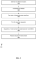
- FIG. 2 is a flowchart of a first embodiment for producing a thermopile IR sensor. Steps of the process 200 are illustrated in FIGS. 1A-1F . It should be noted that any process descriptions or blocks in flowcharts should be understood as representing modules, segments, portions of code, or steps that include one or more instructions for implementing specific logical functions in the process, and alternative implementations are included within the scope of the present invention in which functions may be executed out of order from that shown or discussed, including substantially concurrently or in reverse order, depending on the functionality involved, as would be understood by those reasonably skilled in the art of the present invention.
- CMOS transistors 130 and a CMOS circuit 135 are fashioned on a silicon substrate 110 prepared with a first silicon dioxide layer 120.
- CMOS processing may be used to fashion the substrate 110, for example, Germanium.
- a thin reflector 140 formed of highly doped silicon is implanted in the substrate 110 beneath the silicon dioxide layer 120, as shown by block 220 and FIG. 1B , for example, using ion implantation or diffusion.
- a polysilicon thermopile 150 is formed above the reflector 140, including a silicon spacer 155, overlaid with a second silicon dioxide layer 125.
- a wafer of n-type sensing silicon 160 and a wafer of p-type sensing silicon 165 are formed above the second silicon dioxide layer 125 above the silicon spacer 155.
- the thickness of the silicon spacer 155 may be determined according to the desired detected wavelength, as described below.
- metal contacts 170 for the thermopile 150, and CMOS transistors 130 are deposited, along with a thin film absorber 175 between the wafer of n-type sensing silicon 160 and the wafer of p-type sensing silicon 165.
- the absorber may be formed of, for example, TiN or NiCr or doped silicon, among other CMOS compatible materials that can reach 377 ⁇ /sq.
- the absorber 175 can absorb greater than 85 percent of the incident IR-light in a wavelength of 8-14 ⁇ m, by choosing an appropriate doping concentration and energy for the reflector 140.
- the reflector may cover a wavelength range of 8 ⁇ m-14 ⁇ m with a peak doping concentration after annealing of greater than 10 20 /cm 3 .
- the doping energy may be 70 KeV for boron Ion implantation or 160 KeV for phosphorous Ion implantation.
- the absorber 175 serves as an electrical connector between the wafer of n-type sensing silicon 160 and the wafer of p-type sensing silicon 165.
- a passivation layer 180 is applied.
- the passivation layer 180 material may be, for example, SiO 2 , which is selective to the release step gas, as described below.
- a release step is performed to release the thermopile membrane 150, and a second metal contact 190 is formed.
- the silicon spacer 155 is etched using a highly selective gas, for example, Xenondifluoride XeF 2 , etching only the silicon and not attacking the SiO 2 , for example, the second silicon dioxide layer 125 and the passivation layer 180 surrounding and protecting the thermopile sensing elements 160,165.
- a highly selective gas for example, Xenondifluoride XeF 2
- the reflective behavior of highly doped silicon can be described by a free electron model derived from the Drude model.
- ⁇ p the plasma frequency
- n the amount of free electrons
- e elementary charge
- m the mass of the electron
- ⁇ 0 the dielectric constant.
- the higher the free electron concentration (doping concentration in silicon) the higher the plasma frequency becomes, for example, far infrared.
- the reflector 140 is therefore highly temperature stable and able to survive a dopant activation step of the thermopile sensing materials 160, 165. Due to the miniaturized structure, front-side gas release steps, as mentioned above, can be used and therefore eliminate undercut release steps of traditional thermopiles, preventing loss of pixel area and enabling focal plane array (FPA) integration.
- FPA focal plane array
- the thickness of the doped sensing material 160, 165 can be minimized, which in turn decreases the thermal conductivity ⁇ th and the thermal capacity C th of the sensor 100, in order to keep the thermal time constant ⁇ th in the optimal value. This provides a significant advantage in terms of sensitivity over traditional sensors.
- the Seebeck coefficient may significantly increase and the thermal conductivity may decrease (as known from silicon nanowires) and therefore enhance the sensitivity.
- decreasing the thickness of the sensing material from 300 nm to 150 nm will increase the detectivity by around two times.
- the relationship of thickness to detectivity is an approximately linear.
- a decrease in thickness from 300 nm to 50 nm will implement a detectivity increase of nearly 6 times.
- FIG. 6A is a cross sectional schematic diagram of a thermopile 600 under the first embodiment.
- FIG. 6B is a top view schematic diagram of an exemplary layout of the thermopile 600 under the first embodiment.
- the surface micro machined thermopile sensor process 200 is suitable for the concurrent integration of CMOS circuitry and on-wafer vacuum packaging and can be applied to diode-bolometers, and/or novel resistive microbolometers such as polycrystalline microbolometers or other semi conductive sensing materials in the same manner, which require high temperature processes after forming the reflector.
- the vacuum packaging removes the gases (air) around the sensors after the membrane release, as shown by block 260 ( FIG. 2 ), so the heat created on the sensor membrane due to the IR-light absorption may not be transferred from the sensor 150 to the substrate 110 through gas convection, leading to a serious detectivity decrease, since it is desirable to heat-up the sensor 150 as much as possible to detect any signal change.
- the heat can only dissipate through the sensor arms, which is far more effective than having the gas convection effect.
- FIG. 5 is a flowchart of a second embodiment for producing a lateral diode-bolometer sensor. Steps of the process 500 are illustrated in FIGS. 4A-4F .
- CMOS transistors 430 and a CMOS circuit 435 are fashioned on a silicon substrate 410 prepared with a first silicon dioxide layer 420.
- a thin reflector 440 formed of highly doped silicon is implanted in the substrate 410 beneath the silicon dioxide layer 420, as shown by block 520 and FIG. 4B , for example, using ion implantation or diffusion.
- a polysilicon diode-bolometer 450 is formed above the reflector 440, including a silicon spacer 455, overlaid with a second silicon dioxide layer 425.
- a wafer of n-type sensing silicon 460 and a wafer of p-type sensing silicon 465 are formed above the second silicon dioxide layer 425 above the silicon spacer 455.
- the thickness of the silicon spacer 455 may be determined according to the desired detected wavelength, as described below.
- a thin film absorber 475 is deposited above the reflector 440.
- metal contacts 470 for the diode-bolometer 450, and CMOS transistors 430 are deposited.
- the absorber 475 may absorb greater than 85 percent of the incident IR-light in a wavelength of 8-14 ⁇ m with an appropriate choice of doping concentration and energy for the reflector 440.
- the absorber 475 serves as an electrical connector between the wafer of n-type sensing silicon 460 and the wafer of p-type sensing silicon 465.
- a passivation layer 480 is applied, a release step is performed to remove the spacer 455 and forming a cavity 456, and a second metal contact 490 is formed. The release step may be performed substantially similarly as described above regarding the first embodiment.
- FIG. 7A is a cross sectional schematic diagram of a lateral diode-bolometer 700 under the second embodiment.
- FIG. 7B is a top view schematic diagram of the lateral diode-bolometer 700 under the second embodiment.
- FIG. 8A is a cross sectional schematic diagram of a vertical diode-bolometer 800 under a third embodiment
- FIG. 8B is a top view schematic diagram of the vertical diode-bolometer 800 under the third embodiment.
- FIG. 9A is a cross sectional schematic diagram of a resistive microbolometer 900 under a fourth embodiment
- FIG. 9B is a top view schematic diagram of the resistive microbolometer 900 under the fourth embodiment.
- thermopile/diode-bolometer infrared sensors solve the problem of a bulky absorber and large area pixel(s) for thermopile/diode-bolometer infrared sensors and enable drastic miniaturization.
- a highly doped silicon reflector 140 for an interferometric absorber, high temperature processes to fabricate the thermopile sensor 100 can follow without destroying the reflector 140.
- CMOS circuitry and on-wafer vacuum packaging techniques can be well integrated within the thermopile IR sensor process 200 using this novel approach of the doped silicon reflector 140.
- the absorber 175 may be used as an electrical connection between the n-type silicon 160 and the p-type sensing silicon 165, thereby increasing the absorption area, since no metal is necessary for the connection.
- the release step of such a surface micromachined structure may be done directly before chip scale packaging, therefore decreasing the possibility of damaged sensors due to handling.
- the same idea can be applied to production of a diode-bolometer and/or a resistive microbolometer, in order to avoid complex wafer bonding techniques and allow high temperature processes after creating the reflector.
- thermopile IR sensor / diode-bolometer compared with a detectivity of 5 ⁇ 10 8 cmHz 1/2 /W for approximately a 1 mm ⁇ 1 mm pixel size for a traditional thermopile IR sensor / diode-bolometer, under the first embodiment detectivity may be approximately 5 ⁇ 10 8 cmHz 1/2 /W for a 65 ⁇ m ⁇ 65 ⁇ m pixel size, corresponding to a decrease in area of about 200 times less, with a detectivity increase of greater than 15 times. In general, detectors under the first embodiment having significantly less area may provide a similar detectivity response.
- thermopile IR sensor With the replacement of the traditional microbolometer interferometric absorber, which uses metal as reflector, by a highly doped silicon reflector, the thermopile IR sensor can be highly optimized and provide similar process freedom of a low temperature processed microbolometer. Therefore the performance of this sensor may be considered to be almost equivalent to a conventional microbolometer, having low power consumption and high temperature stability.
- thermopile IR sensors use a bulky absorber and back side release processes, which can be eliminated by the first embodiment. Additionally, complex wafer bonding processes for the diode bolometer can be eliminated. New types of novel resistive microbolometers can be created, for example, a polycrystalline microbolometer, due to high temperature stability of the absorber.
- the above embodiments are based on an interferometric absorber made of a highly doped silicon reflector coupled to a thin absorber (TiN, NiCr) within the thermopile/bolometer structure, wherein the distance of both layers should have an optical length of a quarter wavelength.
- the thin absorber of the first embodiment may be on the order of 7 nm for TiN or less than 200 nm for doped silicon, compared with a traditional absorber, which may be on the order of 3.5 ⁇ m thick.
- the absorber itself has a sheet-resistance on the order of approximately 200 ⁇ /sq - 1000 ⁇ /sq, preferably 377 ⁇ /sq, in order to match the atmospheric impedance. Therefore, reflection on this layer can be minimized and an absorption of approximately 50% can be achieved in the first step.
- the rest of the IR light will be reflected by the underlying highly doped silicon reflector and again absorbed in its maximum of the electromagnetic wave (in this case the maximum of the reflected wave is at ⁇ /4, which is the optical length between absorber and reflector). With this principle, reflection of up to 85% or more of the IR light within a wavelength of 8-14 ⁇ m can be achieved.
- a highly controlled gas release processes can be applied, as known from microbolometers, for example, XeF 2 or Vapor HF (VHF) microbolometers, giving control in both the vertical and lateral direction.
- microbolometers for example, XeF 2 or Vapor HF (VHF) microbolometers, giving control in both the vertical and lateral direction.
- VHF Vapor HF
- thermopile sensor By decreasing the mass of the thermopile sensor due to the thin absorber, sensing silicon and suspension arms can be made much thinner, providing advantages in terms of thermal conductivity and Seebeck coefficient. As known from nanowires, the Seebeck coefficient increases with structures thinner than, for example, but not limited to, 100 nm.
- the sensor membrane can be released directly before capping of the lid, using chip scale packaging techniques. Therefore, destruction of the sensing membrane can be minimized due to handling or further process steps.
- the process flow of the above embodiments is aligned with CMOS integration, so that the integration to an array can be realized.
- embodiments may include an array of pixels.
- FIG. 11 is a top view schematic diagram of an array integration of resistive microbolometers of FIGS. 9A-9B under a fifth embodiment.
- the fifth embodiment of a thin film IR sensor may include a CMOS read-out circuit integrated on the same wafer, for example, in an array integration.
- a switch may be incorporated to switch a read-out signal of each pixel in a row.
- This switch and logic can be achieved by using the defined CMOS transistors 210 ( FIG. 2 ) and the metal contact 240 ( FIG. 2 ) to connect these transistors.
- any logic of CMOS is possible with the process flow, such as CMOS transistor logic, thermopile sensor formation, and connection of logic through metal contacts.
- thermopiles under the first embodiment
- arrays of lateral diode-bolometers under the second embodiment
- arrays of vertical diode-bolometers under the third embodiment.
- arrays of any of these devices may be formed as vacuum packages.
Landscapes
- Physics & Mathematics (AREA)
- General Physics & Mathematics (AREA)
- Spectroscopy & Molecular Physics (AREA)
- Engineering & Computer Science (AREA)
- Manufacturing & Machinery (AREA)
- Photometry And Measurement Of Optical Pulse Characteristics (AREA)
Description
- The present invention relates to radiation sensors, and more particularly, is related to infrared radiation sensors.
- Thermopile infrared sensors are well known to possess temperature stability, for example of up to about 300° C, and low power consumption, for example, a U electronic 32x32 microbolometer array with 450 mW power consumption, or an Excelitas 32x32 array with less than 200 mW power consumption. However, since the detectivity of these sensors is known to be low, compared to a conventional resistive microbolometer (a-Si, VOx, herein referred to as "microbolometer"), approaches have been made to compensate this issue by increasing the pixel size. Such sensors with increased pixel sizes include, for example, a sensor having detectivity of 108 cmHz1/2/W and a microbolometer having detectivity of 109 cmHz1/2/W, as well as a thermopile infrared (IR) sensor size of greater than 1 mm × 1 mm, compared to a microbolometer of 25 µm × 25 µm. Therefore, the etching a cavity in the back side of a substrate below the sensor ("back side etch") coupled with a front side undercut release process and a bulky absorber on the front-side of the sensor have been incorporated to build sensors, which may be operated without a vacuum.
- With the development of new complementary metal-oxide-semiconductor (CMOS) process technology, as known from microbolometer sensors, further miniaturization of the thermopile sensor can be reached by using front-side gas release processes. For example, using XeF2 or Vapor HF, an interferometric absorber, and/or thin film deposition and chip-scale or wafer-level packaging techniques, allows the sensor to reach equivalent microbolometer detectivity capabilities for a relatively low cost price.
- Nevertheless, thermopile sensors generally demand high temperature annealing processes in order to activate the dopants of the n-type and p-type silicon, making CMOS readout circuit and common interferometric absorber integration where metal such as aluminum (Al) is used as reflector, impossible.
- The sensor of some traditional thermopile sensors may be released from the front-side. However, with these traditional thermopiles, a bulky absorber needs to be implemented, due to the under-etch of the silicon beneath the sensor. Additionally, the lateral etch control is generally imprecise, making an integration of sensors as an array almost impossible.
- Therefore, there is a need in the industry to overcome one or more of the abovementioned shortcomings.
-
US2010/0031992A1 discloses a thermopile sensor. - The invention provides a method for manufacturing a surface machined thermopile infrared sensor package in accordance with claim 1 and a surface machined thermopile infrared sensor in accordance with claim 6. Additional features of the invention are defined in the dependent claims.
- Other systems, methods and features of the present invention will be or become apparent to one having ordinary skill in the art upon examining the following drawings and detailed description.
- The accompanying drawings are included to provide a further understanding of the invention, and are incorporated in and constitute a part of this specification. The components in the drawings are not necessarily to scale, emphasis instead being placed upon clearly illustrating the principles of the present invention. The first embodiment is in accordance with the claimed invention. The second to fifth embodiments are not in accordance with the claimed invention but are present for illustration purposes only.
-
FIG. 1A is a cross sectional schematic diagram showing a first stage of manufacture of a thermopile under the first embodiment. -
FIG. 1B is a cross sectional schematic diagram showing a second stage of thermopile manufacture. -
FIG. 1C is a cross sectional schematic diagram showing a third stage of thermopile manufacture. -
FIG. 1D is a cross sectional schematic diagram showing a fourth stage of thermopile manufacture. -
FIG. 1E is a cross sectional schematic diagram showing a fifth stage of thermopile manufacture. -
FIG. 1F is a cross sectional schematic diagram showing a sixth stage of thermopile manufacture. -
FIG. 2 is a flowchart of a method for manufacturing the thermopile device ofFIGS. 1A-1F . -
FIG. 3 is a cross sectional schematic diagram showing thermopile manufacture indicating the spacing between the absorber and the reflector. -
FIG. 4A is a cross sectional schematic diagram showing a first stage of manufacture of a diode-bolometer under the second embodiment. -
FIG. 4B is a cross sectional schematic diagram showing a second stage of diode-bolometer manufacture. -
FIG. 4C is a cross sectional schematic diagram showing a third stage of diode-bolometer manufacture. -
FIG. 4D is a cross sectional schematic diagram showing a fourth stage of diode-bolometer manufacture. -
FIG. 4E is a cross sectional schematic diagram showing a fifth stage of diode-bolometer manufacture. -
FIG. 4F is a cross sectional schematic diagram showing a sixth stage of diode-bolometer manufacture. -
FIG. 5 is a flowchart of a method for manufacturing the diode-bolometer device ofFIGS. 4A-4F . -
FIG. 6A is a cross sectional schematic diagram of a thermopile under the first embodiment. -
FIG. 6B is a top view schematic diagram of the thermopile under the first embodiment. -
FIG. 7A is a cross sectional schematic diagram of a lateral diode-bolometer under the second embodiment. -
FIG. 7B is a top view schematic diagram of the lateral diode-bolometer under the second embodiment. -
FIG. 8A is a cross sectional schematic diagram of a vertical diode-bolometer under the third embodiment. -
FIG. 8B is a top view schematic diagram of the vertical diode-bolometer under the third embodiment. -
FIG. 9A is a cross sectional schematic diagram of a resistive microbolometer under the fourth embodiment. -
FIG. 9B is a top view schematic diagram of the resistive microbolometer under the fourth embodiment. -
FIG. 10 is a cross sectional schematic diagram of a vacuum package embodiment of a thermopile. -
FIG. 11 is a top view schematic diagram of an array integration of resistive microbolometers ofFIGS. 9A-9B under a fifth embodiment. - The following definitions are useful for interpreting terms applied to features of the embodiments disclosed herein, and are meant only to define elements within the disclosure. No limitations on terms used within the claims are intended, or should be derived, thereby. Terms used within the appended claims should only be limited by their customary meaning within the applicable arts.
- As used within this disclosure, "substantially" means "very nearly," for example, "substantially uniform" means uniform within normal manufacturing tolerances as would be expected by persons having ordinary skill in the art.
- As used within this disclosure, "thin" means less than about 15 nm for TiN, or less than about 15 nm for NiCr, and less than about 200 nm for doped silicon.
- As used within this disclosure, a thin film interferometric absorber refers to an interferometric absorber having a thin film formed of a material having a sheet resistance on the order of 377 Ω/sq. For example, the material may be TiN, NiCr, doped silicon, or any other material with a sheet resistance of approximately 377 Ω/sq.
- As used within this disclosure, a thin film thermopile/diode-bolometer/resistive microbolometer refers to a sensor membrane which is generally thinner than 2 µm including a sensing material and an absorber layer.
- As used within this disclosure, "temperature stable" refers to stability of a material at temperatures of up to around 1100° C.
- As used within this disclosure, "increased detectivity" generally refers to a detectivity improvement over a benchmark of 5 × 10⁸ cmHz1/2/W for approximately 1 mm × 1 mm pixel size. For example, a 5 × 10⁸ cmHz1/2/W for a 65 µm × 65 µm pixel size would have area on the order of 200 times less than the 1 mm × 1 mm pixel, while providing similar response. Therefore, increased detectivity indicates an improvement of detectivity of up to fifteen times or more.
- As used within this disclosure, highly doped silicon refers to a peak doping concentration after annealing of greater than 1020/cm3.
- Reference will now be made in detail to embodiments of the present invention, examples of which are illustrated in the accompanying drawings. Wherever possible, the same reference numbers are used in the drawings and the description to refer to the same or like parts.
- Exemplary embodiments of the present invention implement a novel, high temperature stable interferometric absorber and an aligned process to incorporate one or more CMOS devices, a thermopile IR sensor, and on-wafer vacuum packaging together. Embodiments include a surface micro machined thermopile sensor having an interferometric absorber based on a highly doped silicon reflector (on a silicon bulk wafer) and an impedance matched, IR absorbing layer, for example, a 7 nm Ti-N approximately 377 Ohm/sq, on the sensor, which are separated by one quarter wavelength distance 310 (
FIG. 3 ) from each other, in order to adjust the absorption for the desired wavelength. For example, the far infrared range (FIR) has a wavelength range of approximately 8 µm-14 µm, therefore an optical distance of approximately 2.5 µm may be used, representing a center quarter wavelength of absorption of 10 µm. - Embodiments include a process for constructing a thermopile IR sensor / diode-bolometer, which enable drastic miniaturization and a detectivity boost. By replacing a traditional microbolometer interferometric absorber which uses metal as reflector, with a highly doped silicon reflector, the thermopile IR sensor can be highly optimized and have similar process freedom as a low temperature processed microbolometer.
-
FIG. 2 is a flowchart of a first embodiment for producing a thermopile IR sensor. Steps of theprocess 200 are illustrated inFIGS. 1A-1F . It should be noted that any process descriptions or blocks in flowcharts should be understood as representing modules, segments, portions of code, or steps that include one or more instructions for implementing specific logical functions in the process, and alternative implementations are included within the scope of the present invention in which functions may be executed out of order from that shown or discussed, including substantially concurrently or in reverse order, depending on the functionality involved, as would be understood by those reasonably skilled in the art of the present invention. - As shown by
block 210 andFIG. 1A ,CMOS transistors 130 and aCMOS circuit 135 are fashioned on asilicon substrate 110 prepared with a firstsilicon dioxide layer 120. Alternatively, other semiconducting material known in CMOS processing may be used to fashion thesubstrate 110, for example, Germanium. Athin reflector 140 formed of highly doped silicon is implanted in thesubstrate 110 beneath thesilicon dioxide layer 120, as shown byblock 220 andFIG. 1B , for example, using ion implantation or diffusion. As shown byblock 230 andFIG. 1C , apolysilicon thermopile 150 is formed above thereflector 140, including asilicon spacer 155, overlaid with a secondsilicon dioxide layer 125. A wafer of n-type sensing silicon 160 and a wafer of p-type sensing silicon 165 are formed above the secondsilicon dioxide layer 125 above thesilicon spacer 155. The thickness of thesilicon spacer 155 may be determined according to the desired detected wavelength, as described below. - As shown by
block 240 andFIG. 1D ,metal contacts 170 for thethermopile 150, andCMOS transistors 130 are deposited, along with athin film absorber 175 between the wafer of n-type sensing silicon 160 and the wafer of p-type sensing silicon 165. The absorber may be formed of, for example, TiN or NiCr or doped silicon, among other CMOS compatible materials that can reach 377 Ω/sq. Theabsorber 175 can absorb greater than 85 percent of the incident IR-light in a wavelength of 8-14 µm, by choosing an appropriate doping concentration and energy for thereflector 140. The reflector may cover a wavelength range of 8µm-14µm with a peak doping concentration after annealing of greater than 1020 /cm3. For example, the doping energy may be 70 KeV for boron Ion implantation or 160 KeV for phosphorous Ion implantation. As described below, theabsorber 175 serves as an electrical connector between the wafer of n-type sensing silicon 160 and the wafer of p-type sensing silicon 165. - As shown by
block 250 andFIG. 1E , apassivation layer 180 is applied. Thepassivation layer 180 material may be, for example, SiO2, which is selective to the release step gas, as described below. As shown byblock 240 andFIG. 1D . As shown byblock 260 andFIG. 1F , a release step is performed to release thethermopile membrane 150, and asecond metal contact 190 is formed. For the release of themembrane 150, thesilicon spacer 155 is etched using a highly selective gas, for example, Xenondifluoride XeF2, etching only the silicon and not attacking the SiO2, for example, the secondsilicon dioxide layer 125 and thepassivation layer 180 surrounding and protecting the thermopile sensing elements 160,165. This suspends and thermally isolates themembrane 150 over acavity 156 above thesilicon substrate 110 wafer. Since no backside release or under-etching of silicon is necessary, very controlled gas release processes can be replied, for example, as per XeF2 or Vapor HF microbolometers. - The reflective behavior of highly doped silicon can be described by a free electron model derived from the Drude model. Herein, free electrons determine the plasma frequency, which leads to reflection of electro-magnetic waves having frequencies lower than the plasma frequency:

- The
reflector 140 is therefore highly temperature stable and able to survive a dopant activation step of thethermopile sensing materials - By decreasing the bulk of the IR absorber when compared to traditional thermopiles, the thickness of the doped
sensing material sensor 100, in order to keep the thermal time constant τth in the optimal value. This provides a significant advantage in terms of sensitivity over traditional sensors. - With the decrease of the thickness of the sensing material over traditional thermopiles, for example, but not limited to, a thickness below 200 nm, the Seebeck coefficient may significantly increase and the thermal conductivity may decrease (as known from silicon nanowires) and therefore enhance the sensitivity. For example, decreasing the thickness of the sensing material from 300 nm to 150 nm will increase the detectivity by around two times. The relationship of thickness to detectivity is an approximately linear. A decrease in thickness from 300 nm to 50 nm will implement a detectivity increase of nearly 6 times.
-
FIG. 6A is a cross sectional schematic diagram of athermopile 600 under the first embodiment.FIG. 6B is a top view schematic diagram of an exemplary layout of thethermopile 600 under the first embodiment. - The surface micro machined
thermopile sensor process 200 is suitable for the concurrent integration of CMOS circuitry and on-wafer vacuum packaging and can be applied to diode-bolometers, and/or novel resistive microbolometers such as polycrystalline microbolometers or other semi conductive sensing materials in the same manner, which require high temperature processes after forming the reflector. As shown byFIG. 10 , the vacuum packaging removes the gases (air) around the sensors after the membrane release, as shown by block 260 (FIG. 2 ), so the heat created on the sensor membrane due to the IR-light absorption may not be transferred from thesensor 150 to thesubstrate 110 through gas convection, leading to a serious detectivity decrease, since it is desirable to heat-up thesensor 150 as much as possible to detect any signal change. By having vacuum around the sensor, the heat can only dissipate through the sensor arms, which is far more effective than having the gas convection effect. -
FIG. 5 is a flowchart of a second embodiment for producing a lateral diode-bolometer sensor. Steps of theprocess 500 are illustrated inFIGS. 4A-4F . As shown byblock 510 andFIG. 4A ,CMOS transistors 430 and aCMOS circuit 435 are fashioned on asilicon substrate 410 prepared with a firstsilicon dioxide layer 420. Athin reflector 440 formed of highly doped silicon is implanted in thesubstrate 410 beneath thesilicon dioxide layer 420, as shown byblock 520 andFIG. 4B , for example, using ion implantation or diffusion. As shown byblock 530 andFIG. 4C , a polysilicon diode-bolometer 450 is formed above thereflector 440, including asilicon spacer 455, overlaid with a secondsilicon dioxide layer 425. A wafer of n-type sensing silicon 460 and a wafer of p-type sensing silicon 465 are formed above the secondsilicon dioxide layer 425 above thesilicon spacer 455. The thickness of thesilicon spacer 455 may be determined according to the desired detected wavelength, as described below. - As shown by
block 540 andFIG. 4D , athin film absorber 475 is deposited above thereflector 440.. As shown byblock 550 andFIG. 4E ,metal contacts 470 for the diode-bolometer 450, andCMOS transistors 430 are deposited. Theabsorber 475 may absorb greater than 85 percent of the incident IR-light in a wavelength of 8-14 µm with an appropriate choice of doping concentration and energy for thereflector 440. As described below, theabsorber 475 serves as an electrical connector between the wafer of n-type sensing silicon 460 and the wafer of p-type sensing silicon 465. As shown byblock 560 andFIG. 4F , apassivation layer 480 is applied, a release step is performed to remove thespacer 455 and forming acavity 456, and asecond metal contact 490 is formed. The release step may be performed substantially similarly as described above regarding the first embodiment. -
FIG. 7A is a cross sectional schematic diagram of a lateral diode-bolometer 700 under the second embodiment.FIG. 7B is a top view schematic diagram of the lateral diode-bolometer 700 under the second embodiment. Persons having ordinary skill in the art will recognize that other variations of the exemplary second embodiment device and method are possible.FIG. 8A is a cross sectional schematic diagram of a vertical diode-bolometer 800 under a third embodiment, andFIG. 8B is a top view schematic diagram of the vertical diode-bolometer 800 under the third embodiment. Similarly,FIG. 9A is a cross sectional schematic diagram of aresistive microbolometer 900 under a fourth embodiment, whileFIG. 9B is a top view schematic diagram of theresistive microbolometer 900 under the fourth embodiment. - The abovementioned embodiments solve the problem of a bulky absorber and large area pixel(s) for thermopile/diode-bolometer infrared sensors and enable drastic miniaturization. By using a highly doped
silicon reflector 140 for an interferometric absorber, high temperature processes to fabricate thethermopile sensor 100 can follow without destroying thereflector 140. CMOS circuitry and on-wafer vacuum packaging techniques can be well integrated within the thermopileIR sensor process 200 using this novel approach of the dopedsilicon reflector 140. At the same time, theabsorber 175 may be used as an electrical connection between the n-type silicon 160 and the p-type sensing silicon 165, thereby increasing the absorption area, since no metal is necessary for the connection. The release step of such a surface micromachined structure may be done directly before chip scale packaging, therefore decreasing the possibility of damaged sensors due to handling. The same idea can be applied to production of a diode-bolometer and/or a resistive microbolometer, in order to avoid complex wafer bonding techniques and allow high temperature processes after creating the reflector. - An objective of the above embodiments is to achieve a new way of constructing a thermopile IR sensor / diode-bolometer, which enables drastic miniaturization and sensitivity boost. For example, compared with a detectivity of 5 × 10⁸ cmHz1/2/W for approximately a 1 mm × 1 mm pixel size for a traditional thermopile IR sensor / diode-bolometer, under the first embodiment detectivity may be approximately 5 × 10⁸ cmHz1/2/W for a 65 µm × 65 µm pixel size, corresponding to a decrease in area of about 200 times less, with a detectivity increase of greater than 15 times. In general, detectors under the first embodiment having significantly less area may provide a similar detectivity response. With the replacement of the traditional microbolometer interferometric absorber, which uses metal as reflector, by a highly doped silicon reflector, the thermopile IR sensor can be highly optimized and provide similar process freedom of a low temperature processed microbolometer. Therefore the performance of this sensor may be considered to be almost equivalent to a conventional microbolometer, having low power consumption and high temperature stability.
- Traditional thermopile IR sensors, as mentioned above, use a bulky absorber and back side release processes, which can be eliminated by the first embodiment. Additionally, complex wafer bonding processes for the diode bolometer can be eliminated. New types of novel resistive microbolometers can be created, for example, a polycrystalline microbolometer, due to high temperature stability of the absorber.
- The above embodiments are based on an interferometric absorber made of a highly doped silicon reflector coupled to a thin absorber (TiN, NiCr) within the thermopile/bolometer structure, wherein the distance of both layers should have an optical length of a quarter wavelength. For example, the thin absorber of the first embodiment may be on the order of 7 nm for TiN or less than 200 nm for doped silicon, compared with a traditional absorber, which may be on the order of 3.5 µm thick.
- The absorber itself has a sheet-resistance on the order of approximately 200 Ω/sq - 1000 Ω/sq, preferably 377Ω/sq, in order to match the atmospheric impedance. Therefore, reflection on this layer can be minimized and an absorption of approximately 50% can be achieved in the first step. The rest of the IR light will be reflected by the underlying highly doped silicon reflector and again absorbed in its maximum of the electromagnetic wave (in this case the maximum of the reflected wave is at λ/4, which is the optical length between absorber and reflector). With this principle, reflection of up to 85% or more of the IR light within a wavelength of 8-14 µm can be achieved. This results in a highly doped silicon reflector which is highly temperature stable compared to the common metal reflector. Therefore, processes like doping activation of sensing the polysilicon layer can follow without destroying the reflector. Additionally, the amount of absorption can be modified with variation of the doping concentration.
- Since no back side release or under-etching of silicon is necessary under the above embodiments, a highly controlled gas release processes can be applied, as known from microbolometers, for example, XeF2 or Vapor HF (VHF) microbolometers, giving control in both the vertical and lateral direction.
- By decreasing the mass of the thermopile sensor due to the thin absorber, sensing silicon and suspension arms can be made much thinner, providing advantages in terms of thermal conductivity and Seebeck coefficient. As known from nanowires, the Seebeck coefficient increases with structures thinner than, for example, but not limited to, 100 nm.
- Another aspect of the absorber is that the sensor membrane can be released directly before capping of the lid, using chip scale packaging techniques. Therefore, destruction of the sensing membrane can be minimized due to handling or further process steps. Overall, the process flow of the above embodiments is aligned with CMOS integration, so that the integration to an array can be realized. For example, embodiments may include an array of pixels.
-
FIG. 11 is a top view schematic diagram of an array integration of resistive microbolometers ofFIGS. 9A-9B under a fifth embodiment. The fifth embodiment of a thin film IR sensor may include a CMOS read-out circuit integrated on the same wafer, for example, in an array integration. In such an array a switch may be incorporated to switch a read-out signal of each pixel in a row. This switch and logic can be achieved by using the defined CMOS transistors 210 (FIG. 2 ) and the metal contact 240 (FIG. 2 ) to connect these transistors. Similarly, any logic of CMOS is possible with the process flow, such as CMOS transistor logic, thermopile sensor formation, and connection of logic through metal contacts. Of course, other exemplary embodiments are also possible, for example, arrays of thermopiles under the first embodiment, arrays of lateral diode-bolometers under the second embodiment, and arrays of vertical diode-bolometers under the third embodiment. Additionally, arrays of any of these devices may be formed as vacuum packages.
Claims (15)
- A method for manufacturing a surface machined thermopile infrared sensor package, comprising the steps of:providing a silicon substrate (110) having a front side surface and a back side surface;defining a transistor (130) on the substrate front side surface;ion implanting within the substrate at the substrate front side surface a highly doped silicon reflector (140) less than 200 nm thick comprising a peak doping concentration after annealing of greater than 1020/cm3;forming a sensor (150) on the substrate front side surface adjacent to the reflector; anddepositing a thin-film absorber (175) upon the sensor,wherein the thin-film absorber (175) is substantially parallel to the reflector (140) with the sensor (150) disposed there between.
- The method of claim 1, further comprising the step of releasing the front side surface of the infrared sensor (150).
- The method of claim 2, wherein the step of releasing the front side surface of the infrared sensor (150) further comprises forming a cavity by etching a spacer (155) between the reflector (140) and the absorber (175).
- The method of claim 3, wherein said etching is a front side surface etching.
- The method of any of claims 1, 2, 3 or 4, further comprising the step of vacuum packaging for further miniaturization of the surface machined infrared sensor package.
- A surface machined thermopile infrared sensor configured to detect a radiation wavelength, comprising:a silicon wafer (110) having a front side and a back side;a highly doped silicon reflector (140) less than 200 nm thick comprising a peak doping concentration after annealing of greater than 1020/cm3 implanted within a portion of the wafer at the front side surface;a thin-film interferometric absorber (175) disposed parallel to the reflector; anda front side infrared sensor (150) disposed between the reflector (140) and the thin-film absorber (175), the front side infrared sensor comprising:an n-type sensing silicon (160); anda p-type sensing silicon (165).
- The sensor of claim 6, wherein the thin-film absorber (175) is impedance matched to atmosphere, and/or the thin-film absorber impedance is on the order of 377 S2/sq.
- The sensor of claim 6 or 7. wherein the wafer back side does not include a recess behind the sensor (150).
- The sensor of claims 6, 7, or 8, wherein the thin film interferometric absorber (175) is disposed a quarter wavelength distance from the reflector (140), wherein the wavelength comprises a radiation wavelength detected by the sensor.
- The sensor of claims 6, 7, 8, or 9, wherein the front side infrared sensor (150) further comprises first and second silicon dioxide layers (120, 125) disposed between the sensor and the reflector (140).
- The sensor of claim 10, wherein the n-type sensing silicon (160) and/or the p-type sensing silicon (165) is less than 200 nm thick.
- The sensor of claim 6 or 7 to 11, further comprising a CMOS read-out circuit integrated on the wafer.
- The sensor of claims 6 to 12, wherein the sensor is at least partially vacuum packaged.
- A two dimensional array of surface machined infrared sensors according to any of claims 6 to 13.
- The sensor of claims 6 to 13, wherein the front side infrared sensor (150) further comprises sensing silicon and/or a suspension arm thinner than 200 nm.
Applications Claiming Priority (1)
| Application Number | Priority Date | Filing Date | Title |
|---|---|---|---|
| US14/484,856 US20160079306A1 (en) | 2014-09-12 | 2014-09-12 | Surface Micro-Machined Infrared Sensor Using Highly Temperature Stable Interferometric Absorber |
Publications (2)
| Publication Number | Publication Date |
|---|---|
| EP2995916A1 EP2995916A1 (en) | 2016-03-16 |
| EP2995916B1 true EP2995916B1 (en) | 2023-07-26 |
Family
ID=54106175
Family Applications (1)
| Application Number | Title | Priority Date | Filing Date |
|---|---|---|---|
| EP15183849.7A Active EP2995916B1 (en) | 2014-09-12 | 2015-09-04 | Surface micro-machined infrared sensor using highly temperature stable interferometric absorber |
Country Status (4)
| Country | Link |
|---|---|
| US (1) | US20160079306A1 (en) |
| EP (1) | EP2995916B1 (en) |
| JP (1) | JP6889981B2 (en) |
| KR (2) | KR102609052B1 (en) |
Families Citing this family (21)
| Publication number | Priority date | Publication date | Assignee | Title |
|---|---|---|---|---|
| US9851258B2 (en) * | 2014-11-04 | 2017-12-26 | Maxim Integrated Products, Inc. | Thermopile temperature sensor with a reference sensor therein |
| US9726547B2 (en) * | 2014-11-25 | 2017-08-08 | Globalfoundries Inc. | Microbolometer devices in CMOS and BiCMOS technologies |
| US9846083B2 (en) * | 2014-12-17 | 2017-12-19 | Maxim Integrated Products, Inc. | Ambient temperature measurement sensor |
| FR3048128B1 (en) * | 2016-02-18 | 2018-05-18 | Centre National De La Recherche Scientifique | THERMOELECTRIC DEVICE |
| US9915567B2 (en) * | 2016-06-28 | 2018-03-13 | Excelitas Technologies Singapore Pte. Ltd. | Unreleased thermopile infrared sensor using material transfer method |
| FR3056292B1 (en) * | 2016-09-22 | 2020-11-20 | Commissariat Energie Atomique | BOLOMETER TYPE ELECTROMAGNETIC RADIATION DETECTION STRUCTURE AND METHOD FOR MANUFACTURING SUCH A STRUCTURE |
| US10923525B2 (en) | 2017-07-12 | 2021-02-16 | Meridian Innovation Pte Ltd | CMOS cap for MEMS devices |
| US10199424B1 (en) * | 2017-07-19 | 2019-02-05 | Meridian Innovation Pte Ltd | Thermoelectric-based infrared detector having a cavity and a MEMS structure defined by BEOL metals lines |
| US10403674B2 (en) | 2017-07-12 | 2019-09-03 | Meridian Innovation Pte Ltd | Scalable thermoelectric-based infrared detector |
| US10636777B2 (en) * | 2017-12-22 | 2020-04-28 | Ams Sensors Uk Limited | Infra-red device |
| CN110044494B (en) * | 2019-03-22 | 2021-04-13 | 清华大学 | A thermal radiation detector array and its manufacturing method |
| WO2020204833A1 (en) | 2019-04-01 | 2020-10-08 | Meridian Innovation Pte Ltd | Monolithic post complementary metal-oxide-semiconductor integration of thermoelectric-based infrared detector |
| EP3947260A1 (en) | 2019-04-01 | 2022-02-09 | Meridian Innovation Pte Ltd | Heterogenous integration of complementary metal-oxide-semiconductor and mems sensors |
| US12631491B2 (en) | 2019-04-02 | 2026-05-19 | Meridian Innovation Pte Ltd | Wafer level vacuum packaging (WLVP) of thermal imaging sensor |
| FI20195772A1 (en) * | 2019-09-16 | 2021-03-17 | Teknologian Tutkimuskeskus Vtt Oy | Thermal detector |
| TWI708409B (en) * | 2019-11-06 | 2020-10-21 | 新唐科技股份有限公司 | Semiconductor device and the manufacturing method of the same |
| TWI734316B (en) * | 2019-12-24 | 2021-07-21 | 新唐科技股份有限公司 | Thermal sensor and manufacturing method thereof |
| US12553776B2 (en) | 2020-05-28 | 2026-02-17 | Meridian Innovation Pte Ltd | Device having a metamaterial-based focusing annulus lens above a MEMS component and method of manufacturing thereof |
| EP4339568A4 (en) * | 2021-05-11 | 2024-10-09 | Panasonic Intellectual Property Management Co., Ltd. | INFRARED SENSOR AND METHOD FOR MANUFACTURING THE INFRARED SENSOR |
| WO2024090197A1 (en) * | 2022-10-25 | 2024-05-02 | パナソニックIpマネジメント株式会社 | Infrared sensor |
| CN118424465B (en) * | 2024-07-05 | 2024-09-24 | 电子科技大学 | A microsystem compatible with spectral spectrometer chip and detector chip |
Citations (1)
| Publication number | Priority date | Publication date | Assignee | Title |
|---|---|---|---|---|
| US20100031992A1 (en) * | 2006-05-30 | 2010-02-11 | Ying Hsu | Large format thermoelectric infrared detector and method of fabrication |
Family Cites Families (12)
| Publication number | Priority date | Publication date | Assignee | Title |
|---|---|---|---|---|
| JPH05203487A (en) * | 1992-01-27 | 1993-08-10 | Matsushita Electric Works Ltd | Infrared light detector element |
| EP0993053A1 (en) * | 1998-10-09 | 2000-04-12 | STMicroelectronics S.r.l. | Infrared detector integrated with a waveguide and method of manufacturing |
| JP3597069B2 (en) * | 1999-01-12 | 2004-12-02 | 日本電気株式会社 | Thermal infrared array sensor for detecting multiple infrared wavelength bands |
| JP3460810B2 (en) * | 1999-07-26 | 2003-10-27 | 日本電気株式会社 | Thermal infrared detector with thermal separation structure |
| JP3921320B2 (en) * | 2000-01-31 | 2007-05-30 | 日本電気株式会社 | Thermal infrared detector and method for manufacturing the same |
| AUPQ897600A0 (en) * | 2000-07-25 | 2000-08-17 | Liddiard, Kevin | Active or self-biasing micro-bolometer infrared detector |
| US7655909B2 (en) * | 2006-01-26 | 2010-02-02 | L-3 Communications Corporation | Infrared detector elements and methods of forming same |
| US7968846B2 (en) * | 2006-05-23 | 2011-06-28 | Regents Of The University Of Minnesota | Tunable finesse infrared cavity thermal detectors |
| US7543981B2 (en) * | 2006-06-29 | 2009-06-09 | Mattson Technology, Inc. | Methods for determining wafer temperature |
| WO2008028512A1 (en) * | 2006-09-08 | 2008-03-13 | Fraunhofer-Gesellschaft zur Förderung der angewandten Forschung e.V. | Bolometer and method for producing a bolometer |
| KR100925214B1 (en) * | 2007-11-29 | 2009-11-06 | 한국전자통신연구원 | Volometer and its manufacturing method |
| DE112011103431T5 (en) * | 2010-10-11 | 2013-09-05 | Ud Holdings, Llc | Superlattice quantum well lnfrarotdetektor |
-
2014
- 2014-09-12 US US14/484,856 patent/US20160079306A1/en not_active Abandoned
-
2015
- 2015-08-10 JP JP2015158266A patent/JP6889981B2/en active Active
- 2015-09-04 EP EP15183849.7A patent/EP2995916B1/en active Active
- 2015-09-10 KR KR1020150128319A patent/KR102609052B1/en active Active
-
2022
- 2022-10-20 KR KR1020220135576A patent/KR20220148772A/en not_active Withdrawn
Patent Citations (1)
| Publication number | Priority date | Publication date | Assignee | Title |
|---|---|---|---|---|
| US20100031992A1 (en) * | 2006-05-30 | 2010-02-11 | Ying Hsu | Large format thermoelectric infrared detector and method of fabrication |
Non-Patent Citations (1)
| Title |
|---|
| BASU S ET AL: "Infrared radiative properties of heavily doped silicon at room temperature", ASME INTERNATIONAL MECHANICAL ENGINEERING CONGRESS AND EXPOSITION, PROCEEDINGS (ASME INTERNATIONAL MECHANICAL ENGINEERING CONGRESS AND EXPOSITION, IMECE 2007,, vol. 8, no. Part B, 1 January 2008 (2008-01-01), pages 1241 - 1253, XP009139765 * |
Also Published As
| Publication number | Publication date |
|---|---|
| KR20160031429A (en) | 2016-03-22 |
| KR20220148772A (en) | 2022-11-07 |
| US20160079306A1 (en) | 2016-03-17 |
| KR102609052B1 (en) | 2023-12-04 |
| EP2995916A1 (en) | 2016-03-16 |
| JP2016061777A (en) | 2016-04-25 |
| JP6889981B2 (en) | 2021-06-18 |
Similar Documents
| Publication | Publication Date | Title |
|---|---|---|
| EP2995916A1 (en) | Surface micro-machined infrared sensor using highly temperature stable interferometric absorber | |
| CN102884627B (en) | Uncooled ir detector and the method for the manufacture of uncooled ir detector | |
| JP4597677B2 (en) | Electromagnetic radiation detection device having an integrated housing with two overlapping detectors | |
| US9227839B2 (en) | Wafer level packaged infrared (IR) focal plane array (FPA) with evanescent wave coupling | |
| EP2802009B1 (en) | Integrated imaging device for infrared radiation and method of production | |
| US8999813B2 (en) | Focal plane array and method for manufacturing the same | |
| JP7394060B2 (en) | infrared device | |
| US8957378B2 (en) | Nano-tip spacers for precise gap control and thermal isolation in MEMS structures | |
| WO2019043299A1 (en) | Thermal detector and thermal detector array | |
| EP2986959B1 (en) | Thin-film encapsulated infrared sensor | |
| US20110140224A1 (en) | Diode bolometer and method for producing a diode bolometer | |
| US10981782B2 (en) | Process for fabricating a device for detecting electromagnetic radiation having an improved encapsulation structure | |
| WO2010147532A1 (en) | Microbolometer semiconductor material | |
| JP7675707B2 (en) | Heat detector | |
| JP2016070935A (en) | Bolometric detector having mim structure of different dimensions | |
| US9929333B1 (en) | IR thermopile sensor with temperature reference formed in front-end process | |
| EP2363888A1 (en) | Focal plane array and method for manufacturing the same | |
| US11015980B2 (en) | Infrared radiation sensors and methods of manufacturing infrared radiation sensors | |
| WO2015193759A1 (en) | Sensor array with self-aligned optical cavities | |
| EP4631102A1 (en) | Methods and systems for fabrication of infrared transparent window wafer with integrated anti-reflection grating structures | |
| EP3152537B1 (en) | Systems and methods for enhanced bolometer response | |
| KR100759013B1 (en) | Non-contact infrared temperature sensor and manufacturing method thereof | |
| EP2840369A1 (en) | Integrated circuit, system and manufacturing method | |
| US20250130110A1 (en) | Microbolometer and method of manufacturing the same | |
| JP2025152904A (en) | Infrared detector element manufacturing method and infrared detector element |
Legal Events
| Date | Code | Title | Description |
|---|---|---|---|
| PUAI | Public reference made under article 153(3) epc to a published international application that has entered the european phase |
Free format text: ORIGINAL CODE: 0009012 |
|
| AK | Designated contracting states |
Kind code of ref document: A1 Designated state(s): AL AT BE BG CH CY CZ DE DK EE ES FI FR GB GR HR HU IE IS IT LI LT LU LV MC MK MT NL NO PL PT RO RS SE SI SK SM TR |
|
| AX | Request for extension of the european patent |
Extension state: BA ME |
|
| 17P | Request for examination filed |
Effective date: 20160905 |
|
| RBV | Designated contracting states (corrected) |
Designated state(s): AL AT BE BG CH CY CZ DE DK EE ES FI FR GB GR HR HU IE IS IT LI LT LU LV MC MK MT NL NO PL PT RO RS SE SI SK SM TR |
|
| STAA | Information on the status of an ep patent application or granted ep patent |
Free format text: STATUS: EXAMINATION IS IN PROGRESS |
|
| 17Q | First examination report despatched |
Effective date: 20170109 |
|
| GRAP | Despatch of communication of intention to grant a patent |
Free format text: ORIGINAL CODE: EPIDOSNIGR1 |
|
| STAA | Information on the status of an ep patent application or granted ep patent |
Free format text: STATUS: GRANT OF PATENT IS INTENDED |
|
| INTG | Intention to grant announced |
Effective date: 20230217 |
|
| GRAS | Grant fee paid |
Free format text: ORIGINAL CODE: EPIDOSNIGR3 |
|
| GRAA | (expected) grant |
Free format text: ORIGINAL CODE: 0009210 |
|
| STAA | Information on the status of an ep patent application or granted ep patent |
Free format text: STATUS: THE PATENT HAS BEEN GRANTED |
|
| AK | Designated contracting states |
Kind code of ref document: B1 Designated state(s): AL AT BE BG CH CY CZ DE DK EE ES FI FR GB GR HR HU IE IS IT LI LT LU LV MC MK MT NL NO PL PT RO RS SE SI SK SM TR |
|
| REG | Reference to a national code |
Ref country code: CH Ref legal event code: EP |
|
| REG | Reference to a national code |
Ref country code: IE Ref legal event code: FG4D |
|
| REG | Reference to a national code |
Ref country code: DE Ref legal event code: R096 Ref document number: 602015084737 Country of ref document: DE |
|
| REG | Reference to a national code |
Ref country code: LT Ref legal event code: MG9D |
|
| REG | Reference to a national code |
Ref country code: NL Ref legal event code: MP Effective date: 20230726 |
|
| REG | Reference to a national code |
Ref country code: AT Ref legal event code: MK05 Ref document number: 1592431 Country of ref document: AT Kind code of ref document: T Effective date: 20230726 |
|
| PG25 | Lapsed in a contracting state [announced via postgrant information from national office to epo] |
Ref country code: NL Free format text: LAPSE BECAUSE OF FAILURE TO SUBMIT A TRANSLATION OF THE DESCRIPTION OR TO PAY THE FEE WITHIN THE PRESCRIBED TIME-LIMIT Effective date: 20230726 |
|
| PG25 | Lapsed in a contracting state [announced via postgrant information from national office to epo] |
Ref country code: GR Free format text: LAPSE BECAUSE OF FAILURE TO SUBMIT A TRANSLATION OF THE DESCRIPTION OR TO PAY THE FEE WITHIN THE PRESCRIBED TIME-LIMIT Effective date: 20231027 |
|
| PG25 | Lapsed in a contracting state [announced via postgrant information from national office to epo] |
Ref country code: IS Free format text: LAPSE BECAUSE OF FAILURE TO SUBMIT A TRANSLATION OF THE DESCRIPTION OR TO PAY THE FEE WITHIN THE PRESCRIBED TIME-LIMIT Effective date: 20231126 |
|
| PG25 | Lapsed in a contracting state [announced via postgrant information from national office to epo] |
Ref country code: SE Free format text: LAPSE BECAUSE OF FAILURE TO SUBMIT A TRANSLATION OF THE DESCRIPTION OR TO PAY THE FEE WITHIN THE PRESCRIBED TIME-LIMIT Effective date: 20230726 Ref country code: RS Free format text: LAPSE BECAUSE OF FAILURE TO SUBMIT A TRANSLATION OF THE DESCRIPTION OR TO PAY THE FEE WITHIN THE PRESCRIBED TIME-LIMIT Effective date: 20230726 Ref country code: PT Free format text: LAPSE BECAUSE OF FAILURE TO SUBMIT A TRANSLATION OF THE DESCRIPTION OR TO PAY THE FEE WITHIN THE PRESCRIBED TIME-LIMIT Effective date: 20231127 Ref country code: NO Free format text: LAPSE BECAUSE OF FAILURE TO SUBMIT A TRANSLATION OF THE DESCRIPTION OR TO PAY THE FEE WITHIN THE PRESCRIBED TIME-LIMIT Effective date: 20231026 Ref country code: LV Free format text: LAPSE BECAUSE OF FAILURE TO SUBMIT A TRANSLATION OF THE DESCRIPTION OR TO PAY THE FEE WITHIN THE PRESCRIBED TIME-LIMIT Effective date: 20230726 Ref country code: LT Free format text: LAPSE BECAUSE OF FAILURE TO SUBMIT A TRANSLATION OF THE DESCRIPTION OR TO PAY THE FEE WITHIN THE PRESCRIBED TIME-LIMIT Effective date: 20230726 Ref country code: IS Free format text: LAPSE BECAUSE OF FAILURE TO SUBMIT A TRANSLATION OF THE DESCRIPTION OR TO PAY THE FEE WITHIN THE PRESCRIBED TIME-LIMIT Effective date: 20231126 Ref country code: HR Free format text: LAPSE BECAUSE OF FAILURE TO SUBMIT A TRANSLATION OF THE DESCRIPTION OR TO PAY THE FEE WITHIN THE PRESCRIBED TIME-LIMIT Effective date: 20230726 Ref country code: GR Free format text: LAPSE BECAUSE OF FAILURE TO SUBMIT A TRANSLATION OF THE DESCRIPTION OR TO PAY THE FEE WITHIN THE PRESCRIBED TIME-LIMIT Effective date: 20231027 Ref country code: FI Free format text: LAPSE BECAUSE OF FAILURE TO SUBMIT A TRANSLATION OF THE DESCRIPTION OR TO PAY THE FEE WITHIN THE PRESCRIBED TIME-LIMIT Effective date: 20230726 Ref country code: AT Free format text: LAPSE BECAUSE OF FAILURE TO SUBMIT A TRANSLATION OF THE DESCRIPTION OR TO PAY THE FEE WITHIN THE PRESCRIBED TIME-LIMIT Effective date: 20230726 |
|
| PG25 | Lapsed in a contracting state [announced via postgrant information from national office to epo] |
Ref country code: PL Free format text: LAPSE BECAUSE OF FAILURE TO SUBMIT A TRANSLATION OF THE DESCRIPTION OR TO PAY THE FEE WITHIN THE PRESCRIBED TIME-LIMIT Effective date: 20230726 |
|
| PG25 | Lapsed in a contracting state [announced via postgrant information from national office to epo] |
Ref country code: ES Free format text: LAPSE BECAUSE OF FAILURE TO SUBMIT A TRANSLATION OF THE DESCRIPTION OR TO PAY THE FEE WITHIN THE PRESCRIBED TIME-LIMIT Effective date: 20230726 |
|
| REG | Reference to a national code |
Ref country code: DE Ref legal event code: R097 Ref document number: 602015084737 Country of ref document: DE |
|
| PG25 | Lapsed in a contracting state [announced via postgrant information from national office to epo] |
Ref country code: SM Free format text: LAPSE BECAUSE OF FAILURE TO SUBMIT A TRANSLATION OF THE DESCRIPTION OR TO PAY THE FEE WITHIN THE PRESCRIBED TIME-LIMIT Effective date: 20230726 Ref country code: RO Free format text: LAPSE BECAUSE OF FAILURE TO SUBMIT A TRANSLATION OF THE DESCRIPTION OR TO PAY THE FEE WITHIN THE PRESCRIBED TIME-LIMIT Effective date: 20230726 Ref country code: ES Free format text: LAPSE BECAUSE OF FAILURE TO SUBMIT A TRANSLATION OF THE DESCRIPTION OR TO PAY THE FEE WITHIN THE PRESCRIBED TIME-LIMIT Effective date: 20230726 Ref country code: EE Free format text: LAPSE BECAUSE OF FAILURE TO SUBMIT A TRANSLATION OF THE DESCRIPTION OR TO PAY THE FEE WITHIN THE PRESCRIBED TIME-LIMIT Effective date: 20230726 Ref country code: DK Free format text: LAPSE BECAUSE OF FAILURE TO SUBMIT A TRANSLATION OF THE DESCRIPTION OR TO PAY THE FEE WITHIN THE PRESCRIBED TIME-LIMIT Effective date: 20230726 Ref country code: CZ Free format text: LAPSE BECAUSE OF FAILURE TO SUBMIT A TRANSLATION OF THE DESCRIPTION OR TO PAY THE FEE WITHIN THE PRESCRIBED TIME-LIMIT Effective date: 20230726 Ref country code: SK Free format text: LAPSE BECAUSE OF FAILURE TO SUBMIT A TRANSLATION OF THE DESCRIPTION OR TO PAY THE FEE WITHIN THE PRESCRIBED TIME-LIMIT Effective date: 20230726 |
|
| REG | Reference to a national code |
Ref country code: CH Ref legal event code: PL |
|
| PG25 | Lapsed in a contracting state [announced via postgrant information from national office to epo] |
Ref country code: LU Free format text: LAPSE BECAUSE OF NON-PAYMENT OF DUE FEES Effective date: 20230904 |
|
| REG | Reference to a national code |
Ref country code: BE Ref legal event code: MM Effective date: 20230930 |
|
| PG25 | Lapsed in a contracting state [announced via postgrant information from national office to epo] |
Ref country code: LU Free format text: LAPSE BECAUSE OF NON-PAYMENT OF DUE FEES Effective date: 20230904 Ref country code: IT Free format text: LAPSE BECAUSE OF FAILURE TO SUBMIT A TRANSLATION OF THE DESCRIPTION OR TO PAY THE FEE WITHIN THE PRESCRIBED TIME-LIMIT Effective date: 20230726 Ref country code: MC Free format text: LAPSE BECAUSE OF FAILURE TO SUBMIT A TRANSLATION OF THE DESCRIPTION OR TO PAY THE FEE WITHIN THE PRESCRIBED TIME-LIMIT Effective date: 20230726 |
|
| PLBE | No opposition filed within time limit |
Free format text: ORIGINAL CODE: 0009261 |
|
| STAA | Information on the status of an ep patent application or granted ep patent |
Free format text: STATUS: NO OPPOSITION FILED WITHIN TIME LIMIT |
|
| 26N | No opposition filed |
Effective date: 20240429 |
|
| REG | Reference to a national code |
Ref country code: IE Ref legal event code: MM4A |
|
| PG25 | Lapsed in a contracting state [announced via postgrant information from national office to epo] |
Ref country code: IE Free format text: LAPSE BECAUSE OF NON-PAYMENT OF DUE FEES Effective date: 20230904 |
|
| PG25 | Lapsed in a contracting state [announced via postgrant information from national office to epo] |
Ref country code: CH Free format text: LAPSE BECAUSE OF NON-PAYMENT OF DUE FEES Effective date: 20230930 |
|
| PG25 | Lapsed in a contracting state [announced via postgrant information from national office to epo] |
Ref country code: IE Free format text: LAPSE BECAUSE OF NON-PAYMENT OF DUE FEES Effective date: 20230904 Ref country code: CH Free format text: LAPSE BECAUSE OF NON-PAYMENT OF DUE FEES Effective date: 20230930 Ref country code: SI Free format text: LAPSE BECAUSE OF FAILURE TO SUBMIT A TRANSLATION OF THE DESCRIPTION OR TO PAY THE FEE WITHIN THE PRESCRIBED TIME-LIMIT Effective date: 20230726 |
|
| PG25 | Lapsed in a contracting state [announced via postgrant information from national office to epo] |
Ref country code: BE Free format text: LAPSE BECAUSE OF NON-PAYMENT OF DUE FEES Effective date: 20230930 |
|
| PG25 | Lapsed in a contracting state [announced via postgrant information from national office to epo] |
Ref country code: BG Free format text: LAPSE BECAUSE OF FAILURE TO SUBMIT A TRANSLATION OF THE DESCRIPTION OR TO PAY THE FEE WITHIN THE PRESCRIBED TIME-LIMIT Effective date: 20230726 |
|
| PG25 | Lapsed in a contracting state [announced via postgrant information from national office to epo] |
Ref country code: BG Free format text: LAPSE BECAUSE OF FAILURE TO SUBMIT A TRANSLATION OF THE DESCRIPTION OR TO PAY THE FEE WITHIN THE PRESCRIBED TIME-LIMIT Effective date: 20230726 |
|
| PG25 | Lapsed in a contracting state [announced via postgrant information from national office to epo] |
Ref country code: CY Free format text: LAPSE BECAUSE OF FAILURE TO SUBMIT A TRANSLATION OF THE DESCRIPTION OR TO PAY THE FEE WITHIN THE PRESCRIBED TIME-LIMIT; INVALID AB INITIO Effective date: 20150904 |
|
| PG25 | Lapsed in a contracting state [announced via postgrant information from national office to epo] |
Ref country code: HU Free format text: LAPSE BECAUSE OF FAILURE TO SUBMIT A TRANSLATION OF THE DESCRIPTION OR TO PAY THE FEE WITHIN THE PRESCRIBED TIME-LIMIT; INVALID AB INITIO Effective date: 20150904 |
|
| PGFP | Annual fee paid to national office [announced via postgrant information from national office to epo] |
Ref country code: DE Payment date: 20250929 Year of fee payment: 11 |
|
| PGFP | Annual fee paid to national office [announced via postgrant information from national office to epo] |
Ref country code: GB Payment date: 20250929 Year of fee payment: 11 |
|
| PGFP | Annual fee paid to national office [announced via postgrant information from national office to epo] |
Ref country code: FR Payment date: 20250925 Year of fee payment: 11 |
|
| PG25 | Lapsed in a contracting state [announced via postgrant information from national office to epo] |
Ref country code: TR Free format text: LAPSE BECAUSE OF FAILURE TO SUBMIT A TRANSLATION OF THE DESCRIPTION OR TO PAY THE FEE WITHIN THE PRESCRIBED TIME-LIMIT Effective date: 20230726 |