EP2994318B1 - Nanostructure array diffractive optics for motion and animation display - Google Patents
Nanostructure array diffractive optics for motion and animation display Download PDFInfo
- Publication number
- EP2994318B1 EP2994318B1 EP14795088.5A EP14795088A EP2994318B1 EP 2994318 B1 EP2994318 B1 EP 2994318B1 EP 14795088 A EP14795088 A EP 14795088A EP 2994318 B1 EP2994318 B1 EP 2994318B1
- Authority
- EP
- European Patent Office
- Prior art keywords
- nanostructure
- display device
- frame
- substrate
- arrays
- Prior art date
- Legal status (The legal status is an assumption and is not a legal conclusion. Google has not performed a legal analysis and makes no representation as to the accuracy of the status listed.)
- Revoked
Links
Images


Classifications
-
- G—PHYSICS
- G02—OPTICS
- G02B—OPTICAL ELEMENTS, SYSTEMS OR APPARATUS
- G02B5/00—Optical elements other than lenses
- G02B5/18—Diffraction gratings
- G02B5/1842—Gratings for image generation
-
- B—PERFORMING OPERATIONS; TRANSPORTING
- B42—BOOKBINDING; ALBUMS; FILES; SPECIAL PRINTED MATTER
- B42D—BOOKS; BOOK COVERS; LOOSE LEAVES; PRINTED MATTER CHARACTERISED BY IDENTIFICATION OR SECURITY FEATURES; PRINTED MATTER OF SPECIAL FORMAT OR STYLE NOT OTHERWISE PROVIDED FOR; DEVICES FOR USE THEREWITH AND NOT OTHERWISE PROVIDED FOR; MOVABLE-STRIP WRITING OR READING APPARATUS
- B42D25/00—Information-bearing cards or sheet-like structures characterised by identification or security features; Manufacture thereof
- B42D25/30—Identification or security features, e.g. for preventing forgery
- B42D25/324—Reliefs
-
- B—PERFORMING OPERATIONS; TRANSPORTING
- B42—BOOKBINDING; ALBUMS; FILES; SPECIAL PRINTED MATTER
- B42D—BOOKS; BOOK COVERS; LOOSE LEAVES; PRINTED MATTER CHARACTERISED BY IDENTIFICATION OR SECURITY FEATURES; PRINTED MATTER OF SPECIAL FORMAT OR STYLE NOT OTHERWISE PROVIDED FOR; DEVICES FOR USE THEREWITH AND NOT OTHERWISE PROVIDED FOR; MOVABLE-STRIP WRITING OR READING APPARATUS
- B42D25/00—Information-bearing cards or sheet-like structures characterised by identification or security features; Manufacture thereof
- B42D25/30—Identification or security features, e.g. for preventing forgery
- B42D25/328—Diffraction gratings; Holograms
-
- B—PERFORMING OPERATIONS; TRANSPORTING
- B42—BOOKBINDING; ALBUMS; FILES; SPECIAL PRINTED MATTER
- B42D—BOOKS; BOOK COVERS; LOOSE LEAVES; PRINTED MATTER CHARACTERISED BY IDENTIFICATION OR SECURITY FEATURES; PRINTED MATTER OF SPECIAL FORMAT OR STYLE NOT OTHERWISE PROVIDED FOR; DEVICES FOR USE THEREWITH AND NOT OTHERWISE PROVIDED FOR; MOVABLE-STRIP WRITING OR READING APPARATUS
- B42D25/00—Information-bearing cards or sheet-like structures characterised by identification or security features; Manufacture thereof
- B42D25/40—Manufacture
- B42D25/405—Marking
-
- G—PHYSICS
- G02—OPTICS
- G02B—OPTICAL ELEMENTS, SYSTEMS OR APPARATUS
- G02B5/00—Optical elements other than lenses
- G02B5/18—Diffraction gratings
- G02B5/1809—Diffraction gratings with pitch less than or comparable to the wavelength
-
- G—PHYSICS
- G02—OPTICS
- G02B—OPTICAL ELEMENTS, SYSTEMS OR APPARATUS
- G02B5/00—Optical elements other than lenses
- G02B5/18—Diffraction gratings
- G02B5/1814—Diffraction gratings structurally combined with one or more further optical elements, e.g. lenses, mirrors, prisms or other diffraction gratings
- G02B5/1819—Plural gratings positioned on the same surface, e.g. array of gratings
- G02B5/1823—Plural gratings positioned on the same surface, e.g. array of gratings in an overlapping or superposed manner
-
- G—PHYSICS
- G02—OPTICS
- G02B—OPTICAL ELEMENTS, SYSTEMS OR APPARATUS
- G02B5/00—Optical elements other than lenses
- G02B5/18—Diffraction gratings
- G02B5/1828—Diffraction gratings having means for producing variable diffraction
-
- H—ELECTRICITY
- H01—ELECTRIC ELEMENTS
- H01J—ELECTRIC DISCHARGE TUBES OR DISCHARGE LAMPS
- H01J37/00—Discharge tubes with provision for introducing objects or material to be exposed to the discharge, e.g. for the purpose of examination or processing thereof
- H01J37/30—Electron-beam or ion-beam tubes for localised treatment of objects
- H01J37/317—Electron-beam or ion-beam tubes for localised treatment of objects for changing properties of the objects or for applying thin layers thereon, e.g. for ion implantation
- H01J37/3174—Particle-beam lithography, e.g. electron beam lithography
-
- B—PERFORMING OPERATIONS; TRANSPORTING
- B82—NANOTECHNOLOGY
- B82Y—SPECIFIC USES OR APPLICATIONS OF NANOSTRUCTURES; MEASUREMENT OR ANALYSIS OF NANOSTRUCTURES; MANUFACTURE OR TREATMENT OF NANOSTRUCTURES
- B82Y20/00—Nanooptics, e.g. quantum optics or photonic crystals
Definitions
- the present invention relates generally to optical security displays, and more particularly to optical security motion and animation displays using nanostructure arrays, and methods for their manufacture and use.
- diffraction gratings which may consist of periodic structures which cause incident light to diffract.
- diffraction may occur both in transmissive (e.g. prisms) or reflective (e.g. CDs and DVDs) modes, and such diffraction may be due to the transparency or reflective nature of the substrate which contains the periodic structure.
- the pitch or spacing of the periodic structures which is typically known as the period of the grating, has an inverse effect on the dispersion angle.
- an array of nanoholes with periodicity in the visible spectrum ( ⁇ ) and hole diameters smaller than ⁇ /2 may also diffract light to create structural colors.
- the physical configuration of the nano-features may define the intensity of the diffracted wavelengths which may be substantially higher than which may be obtained using more conventionally available micro-scale gratings.
- the intensity of the maxima peaks, in transmission or reflection increases as a function of the number of slits (N) over a given area, specifically increasing as N 2 .
- the colors seen in the first order maxima peaks become more distinguishable leading too higher chromatic resolution - i.e. crisper and clearer defined colors.
- a diffraction grating with a spacing of 500 nm will exhibit intensity four times that of a grating spaced at 1000nm, while producing clearly defined color bars.
- the nanoscale features appear brighter, especially noticeable in dimmer light, and their specific colors appear more solid as the viewing angle changes (i.e. less "rainbowing" of colors).
- Diffraction gratings split white light into multiple colors.
- nano-scale gratings Due to their unique brilliant optical effects, these nano-scale gratings have been implemented in some applications to replace holograms such as for some security applications in some aspects known in the art.
- motion and animation optical displays which provide the appearance or illusion of motion using multiple frames of a similar or related image shown in different positions, and exposing one frame at a time to a viewer.
- a shutter or grating layer may be moved over a second layer showing multiple overlapping frames interlayered with each other to show successive frames to a viewer, such as in a "scanimation" type shutter animation display.
- one or more of diffraction grating secondary layers, polarization secondary layers, lenticular lenses, holographic interference patterns and/or light wave interference may be used to alternate or selectively view individual image frames in other motion or animation displays.
- Certain features, aspects and examples disclosed herein are directed to motion and animation displays using nanostructure arrays, according to an embodiment of the present invention. Certain features, aspects and examples are further directed to a method of manufacturing motion and animation displays using nanostructure arrays, according to another embodiment of the present invention. Additional features, aspects and examples are discussed in more detail herein.
- the invention is defined in claim 1.
- a motion and animation display comprising multiple nanostructure arrays oriented at differing relative angles of rotation corresponding to multiple frames of an animation image, wherein the multiple nanostructure arrays are formed on a single substrate layer.
- an optical display device comprising a substrate having a surface, a first frame of an animated image comprising a first optical sub-wavelength nanostructure array formed on or in the surface of the substrate, and a second frame of an animated image comprising a second optical sub-wavelength nanostructure array formed on or in the surface of the substrate, where the second nanostructure array is rotated relative to the first nanostructure array by a first relative angle of rotation.
- the optical display device may comprise an optical security device, and the animated image comprises optically visible features and is operable to visually authenticate an article comprising the optical security device.
- the optical display device may comprise a first nanostructure array operable to diffract an incident light source at a first viewable angle relative to the substrate, and a second nanostructure array operable to diffract an incident light source at a second viewable angle relative to the substrate, such that the first frame of the animated image is viewable at the first viewing angle and the second frame of the animated image is viewable at the second viewing angle.
- the optical display device comprises a first nanostructure array comprising a plurality of nanostructures arranged in a first periodic lattice, and a second nanostructure array comprising a plurality of nanostructures arranged in a second periodic lattice, where the second periodic lattice is rotated relative to the first periodic lattice by a first relative angle of rotation.
- a method of manufacturing a motion and animation display comprising multiple nanostructure arrays oriented at differing relative angles of rotation is provided.
- a method of manufacturing an optical display device comprising providing a substrate comprising a surface, forming a first plurality of optical sub-wavelength nanostructure arrays on the substrate surface to form a first frame of an animated image, and forming a second plurality of optical sub-wavelength nanostructure arrays on said substrate surface to form a second frame of an animated image where the second nanostructure arrays are rotated relative to the first nanostructure arrays by a first relative angle of rotation.
- forming the first and second pluralities of nanostructure arrays comprises one or more of printing, imprinting, embossing, stamping, molding, etching or inscribing the nanostructure arrays in or on the substrate surface.
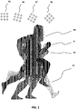
- FIG. 1 a schematic view of an exemplary animation or motion display is shown comprising multiple interleaved image frames 11, 12, 13 and 14, each frame comprising nanostructure arrays such as representative corresponding nanohole arrays 15, 16, 17 and 18, arranged at a predetermined rotational orientation relative to each other frame, according to an embodiment of the present invention.
- four image frames 11, 12, 13 and 14 are overlaid and/or interleaved with each other on a single layer substrate to form a composite interleaved image.
- Each of the exemplary four frames 11, 12, 13, 14 comprises nanostructure arrays formed on or in the substrate surface, where the corresponding nanostructure arrays representing each frame is oriented at a unique lattice angle relative to the other frames, to allow for only one of the four frames to be visible to a viewer at a particular viewing angle, due to the different angle of diffraction produced by the nanostructure arrays of each frame which diffract light at different viewing angles.
- first frame 11 may comprise nanostructure arrays, such as exemplary nanohole arrays 15 oriented at a first relative lattice angle of 0 degrees.
- Second frame 12 may comprise nanostructure arrays, such as exemplary nanohole arrays 16 rotated at a second lattice angle such as 15 degrees relative to first arrays 15.
- Third frame 13 may comprise nanostructure arrays, such as exemplary nanohole arrays 17 rotated at a third lattice angle such as 30 degrees.
- Fourth frame 14 may comprise nanostructure arrays, such as exemplary nanohole arrays 18 rotated at a fourth lattice angle such as 45 degrees.
- a motion or animation display may comprise multiple image frames overlaid and interleaved with each other on a single layer substrate surface, such as by separating each frame into fine lines (such as "slicing" into vertical lines) and interleaving each frame with the other frames to form a composite interleaved image on a single layer substrate surface, such as may be similar to the appearance of a design prepared for use with a "sc animation" multi-layer moving shutter animation system, wherein the animation or motion effect occurs in a single area of the substrate, such as in the case of the exemplary four frame animation of a running person such as is shown in FIG. 1 .
- FIG. 1 In an exemplary embodiment such as that shown in FIG.
- each line of each frame may comprise nanohole arrays, such that all of the lines in a single frame are formed from nanohole arrays oriented at the same predetermined relative lattice rotational angle, and may therefore be seen at a particular predetermined viewing angle due to the diffraction effect of the predetermined lattice rotational angle.
- the rotational angle for each frame 11 is different relative to the rotation angle of the nanohole lattices of the other frames 12, 13, 14, so that the different diffractive angles resulting from each of the nanohole lattice angles results in only a single frame of the display being visible at a range of specific viewing angles by a viewer, while the other frames are not simultaneously visible.
- the viewer can then trigger or view the sequential animation or motion display by rotating the display or tilting the display left/right or up/down, such that the viewing angle changes, and each frame of the display can be individually sequentially viewed to form the motion or animation effect of the display - which in the exemplary display shown in FIG. 1 would appear to be a person running in place.
- all the nanostructure arrays of a single frame, or of all the frames in an exemplary animation or motion display may comprise a single periodicity and nanostructure size, so that the entire frame, or all of the frames appear in a single color to form a monochrome image.
- the nanostructure arrays of different frames may have different periodicities and sizes so that different frames appear as different colors, or alternatively, each frame may comprise nanohole arrays having different specific periodicities and sizes chosen by a designer to provide different colors so as to allow for color imagery of each frame.
- the nanohole arrays of each frame may be arranged in subgroups or areas such as to define sub-images or pixels of an image, and the periodicity and size of the nanostructure arrays in each sub-image or pixel may be selected to define a particular color or brightness, so as to allow for complex color image representations of each frame in the animation or motion display.
- the nanostructure arrays used to form each frame of an exemplary animation or motion display may comprise any suitable periodic nanostructure array that may be used to provide a diffractive effect on incident light, such as periodic sub-wavelength nanohole arrays, or such as nano-columns, which may be formed in a periodic nanostructure array on any suitable substrate surface, such as by nano-imprinting, embossing, machining, deposition or any other suitable nanostructure formation technique.
- suitable substrates may comprise but are not limited to films, surfaces or layers of metallic, polymer, composite, cellulose, non-metallic or other suitable substrate materials, for example.
- FIG. 2 a schematic view of exemplary nanostructure arrays for providing selective diffraction of incident light is shown, according to an embodiment of the invention.
- An exemplary first nanostructure array such as nanohole array 22, which is oriented at a first relative rotational angle, may act to diffract a diffuse incident light source 23, to form diffracted light 24 which is diffracted at a characteristic angle and viewable by a viewer or observer 21 at a particular viewing angle or range of viewing angles relative to the location of the nanohole array 22.
- An exemplary second nanostructure array such as nanohole array 25 is oriented at a second relative rotational angle with respect to the first array 22, such that diffuse incident light is diffracted to form second diffracted light beam 26, which is diffracted at a different characteristic angle, and would not be viewable by the observer 21 at the same position as the diffracted light 24 from the first nanohole array 22. Therefore, similar to as is described above in reference to FIG. 1 , the different relative rotational angles of the nanohole arrays 22 and 25 provide for selective viewability of the diffracted light from the nanohole arrays, depending on the position of an observer. In one embodiment of the invention such as shown in FIG.
- this selective viewability allows for a viewer to view separate image frames comprising nanohole arrays rotated at different angles on a single substrate surface, such that each frame is separately and individually viewable in sequence as the viewer or observer rotates, or tilts the substrate to vary the relative viewing angle of the diffracted light coming from the nanohole arrays of each frame in sequence, such as to provide for motion or animation effects of the display
- the incident diffuse light 23 may be diffracted and reflected and/or transmitted by the nanohole arrays forming the animation or motion display.
- a motion or animation display may be applied as an optical security device comprising a substrate imprinted or embossed with sub-wavelength nanostructure arrays such as nanohole arrays, to create a motion or animation effect via diffraction of reflected or transmitted incident light that can be used to visually authenticate a separate entity or article (such as a document, currency, component or other security item) that may contain the substrate.
- An optical security device may use specific sets of periodic sub-wavelength nanohole arrays to create bright diffractive based images that exhibit motion-like or animation effects when selectively and sequentially viewed by an observer.
- the images may be multi-color or monochrome (single color).
- rotating a finite nanohole array lattice angle may provide for control of the angle of diffracted light reflected or transmitted from the arrays, and thus the viewable angle of individual frames or portions of the imagery, can be tuned.
- sets of nanostructure arrays orientated at various rotations forming separate image frames may be used to create animations or simulated motion effects.
- an observer or viewer may activate the motion / animation effect(s) of the display by changing the viewing angle of an image consisting of such nanohole array sets, such as changing the viewing angle simply by rotating or tilting the display or substrate.
- the nanohole arrays can be configured and treated as pixels that can be less than a micron in size, allowing for extremely high-resolution imagery to be produced.
- the diffraction characteristics and high resolution imagery that can be produced using sub-wavelength nanohole arrays are unique and therefore replication of these effects using any other technique would be expected to be difficult, if not improbable, making this technology highly suitable for security optics applications.
- exemplary nanostructure arrays used to form motion or animation displays may be configured such that the difference between rotational angles of adjacent image frames in an animation or motion sequence of the display are substantially equal, so that the animation or motion appears to move at substantially the same speed between image frames.
- the arrays may be configured such that the difference between rotational angles of adjacent image frames in an animation or motion sequence of the display vary from frame to frame, so that the animation or motion appears to accelerate and/or decelerate between image frames, as may be desired to provide for more varied appearance of animation or motion effects of the display, for example.
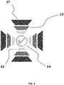
- FIG. 3 a plan view of an exemplary animation or motion display comprising multiple adjacent image frames 31, 32, 33, 34, each frame comprising nanostructure arrays arranged at a predetermined rotational orientation relative to each other frame is shown, according to an embodiment of the invention.
- the four animation frames 31, 32, 33, 34 are arranged to simulate motion towards a vanishing point, and an exemplary central positive authentication indicia (check mark image 34), and are adjacent to each other and not overlaid or interleaved, so as to provide for a simulated motion effect moving toward the central area as the image frames 31, 32, 33, 34 are viewed individually in sequence.
- check mark image 34 exemplary central positive authentication indicia
- each image frame 31, 32, 33, 34 may be configured from nanostructure arrays, such as nanohole arrays, with different unique nanostructure array lattice rotation angles.
- each individual frame 31, 32, 33, 34 may also comprise nanostructure arrays having different unique periodicities and/or nanostructure sizes in addition to their different rotational angles, so as to provide for differences in at least one of the color, brightness, or quality of the image frame as viewed by a viewer, such as may be used to accentuate a motion or animation effect of the display, such as the lightening color of the concentric bars of frames 31, 32, 33, and the different color of the central indicia frame 34, for example.
- frame 3 may comprise square lattice nanohole arrays where frame 31 comprises nanohole arrays with a periodicity of 450 nm and a relative lattice rotational angle of 0 degrees; frame 32 comprises nanohole arrays with a periodicity of 470 nm and a relative lattice rotational angle of 10 degrees; frame 33 comprises nanohole arrays with a periodicity of 480 nm and a relative lattice rotational angle of 20 degrees; and frame 34 comprises nanohole arrays with a periodicity of 500 nm and a relative lattice rotational angle of 30 degrees, for example.
- the two frame motion or animation display comprises a first frame 41 showing a blank circle, and a second frame 42 showing an indicia or symbol (such as the exemplary number 7).
- the relative rotation angles of the frames may be selected so that they may absorb light and appear dark at all but a limited desired viewing angle represented by the second frame 42, for example.
- the nanohole arrays of the display when the substrate comprising the display is rotated or tilted to a predetermined angle, the nanohole arrays of the display will reflect diffracted incident light to reveal the desired hidden image or indicia, such as the indicia of second frame 42.
- selection of appropriate periodicity of the nanohole arrays may also allow use of such a two frame display to light up or color a shadow image, for example.
- the display of FIG. 4 may comprise nanohole arrays where frame 41 comprises nanohole arrays with a periodicity of 600 nm and a relative lattice rotational angle of 45 degrees and frame 42 comprises nanohole arrays with a periodicity of 450 nm and a relative lattice rotational angle of 45 degrees.
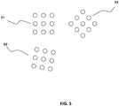
- the square lattice nanostructure arrays may comprise square lattice nanohole arrays 51, 52, 53, where array 51 is oriented at a relative lattice rotation angle of 0 degrees; array 52 is oriented at a relative lattice rotation angle of 10 degrees; and array 53 is oriented at a relative lattice rotation angle of 45 degrees, for example.
- the hexagonal lattice nanostructure arrays may comprise hexagonal lattice nanohole arrays 61, 62, 63, 64 where array 61 is oriented at a relative lattice rotation angle of 0 degrees; array 62 is oriented at a relative lattice rotation angle of 10 degrees; array 63 is oriented at a relative lattice rotation angle of 45 degrees, and array 64 is oriented at a relative lattice rotational angle of 90 degrees, for example.
- a motion or animation display may comprise nanostructure arrays arranged in arrays having lattice configurations comprising at least one of: square, hexagonal, octagonal, pentagonal, or penrose semi-ordered lattice geometries.
- the nanostructure arrays may be arranged in one or more other suitable lattice geometries.
- a motion or animation display may comprise nanostructure arrays comprising nanoholes, where the geometry of the nanoholes comprising the array are selected from one or more of circular, substantially round, elliptical, rectangular, triangular or square hole geometries.
- the nanoholes of the nanostructure arrays may be shaped in one or more other suitable hole geometries.
- a motion of animation display according to the invention may comprise one or more exemplary nanostructure array configurations, such as exemplary square lattice nanohole arrays 71, 72, 73 and 74.
- the spacing or periodicity of a nanohole array may be selected to determine a primary wavelength of light which may be preferentially reflected and/or transmitted by the nanohole array.
- the size of the nanoholes in an array may be selected to determine the relative brightness of the light which may be preferentially reflected and/or transmitted by the nanohole array, and/or the bandwidth or range of wavelengths which may be preferentially reflected and/or transmitted by the nanohole array, for example.
- an optical security device may be provided comprising a single layer substrate imprinted or embossed with sub-wavelength nanohole arrays to create a motion or animation effect via diffraction of reflected or transmitted incident light that can be used to visually authenticate a separate entity that may contain said substrate.
- an optical security device may also comprise at least two sets of nanohole arrays which each exhibit different relative lattice rotation angles around a common axis and at least one pre-defined periodic spacing (periodicity) between the holes of the arrays.
- an optical security device may also comprise at least two sets of nanohole arrays that exhibit at least two different periodicities for producing at least two corresponding first order diffractive colors.
- an optical security device may also comprise nanohole arrays exhibiting at least one periodic array lattice type selected from the list comprising: square, hexagonal octagonal, and penrose semi-ordered lattices.
- an optical security device may also comprise nanohole arrays with at least one specified hole geometry selected from the list comprising: circles, ellipses, rectangles, squares and triangles.
- an optical security device may be provided that comprises at least two images overlaid and/or interleaved (such as shown in FIG. 1 for example) to create a multi-frame animation or motion-like display or effect.
- each image frame may comprise a set of nanohole arrays oriented at at least one unique angle of lattice rotation for each image frame.
- an optical security device may be provided that comprises at least two images separate from, and substantially not overlapping or overlaid onto, each other (such as shown in FIG. 3 for example), to create at least two separate frames of a multi-frame animation or motion-like display or effect.
- each image frame may comprise a set of nanohole arrays oriented with at least one unique lattice rotation angle for each image frame.
- an optical security device may be provided that comprises at least two images (such as shown in FIG. 4 for example) to create a multi-frame animation or motion-like display or effect revealing a hidden image or indicia depending on a viewing angle of an observer.
- each image frame may comprise nanohole arrays having substantially similar or the same lattice rotation angle, but a different periodicity such that the two image frames can be distinguished.
- the optical security device may additionally comprise at least two sets of nanohole arrays that comprise nanohole structures which desirably absorb incident light according to a diffractive property or specified law, thereby concealing at least one image at a specified set of viewing angles.
Landscapes
- Physics & Mathematics (AREA)
- General Physics & Mathematics (AREA)
- Optics & Photonics (AREA)
- Engineering & Computer Science (AREA)
- Manufacturing & Machinery (AREA)
- Chemical & Material Sciences (AREA)
- Analytical Chemistry (AREA)
- Diffracting Gratings Or Hologram Optical Elements (AREA)
- Credit Cards Or The Like (AREA)
Description
- This application is related and claims priority to
US Provisional Patent Application Serial No. 61/821,714 filed May 9, 2013 US Provisional Patent Application Serial No. 61/822,166 filed May 10, 2013 - The present invention relates generally to optical security displays, and more particularly to optical security motion and animation displays using nanostructure arrays, and methods for their manufacture and use.
- According to one aspect of the art, diffraction gratings are known which may consist of periodic structures which cause incident light to diffract. In such cases, diffraction may occur both in transmissive (e.g. prisms) or reflective (e.g. CDs and DVDs) modes, and such diffraction may be due to the transparency or reflective nature of the substrate which contains the periodic structure. In such case, the pitch or spacing of the periodic structures, which is typically known as the period of the grating, has an inverse effect on the dispersion angle.
- In one such aspect according to the art, an array of nanoholes with periodicity in the visible spectrum (λ) and hole diameters smaller than λ/2 may also diffract light to create structural colors. In one such aspect, the physical configuration of the nano-features may define the intensity of the diffracted wavelengths which may be substantially higher than which may be obtained using more conventionally available micro-scale gratings. For any diffraction grating, the intensity of the maxima peaks, in transmission or reflection, increases as a function of the number of slits (N) over a given area, specifically increasing as N2. The colors seen in the first order maxima peaks become more distinguishable leading too higher chromatic resolution - i.e. crisper and clearer defined colors. For example, a diffraction grating with a spacing of 500 nm will exhibit intensity four times that of a grating spaced at 1000nm, while producing clearly defined color bars. Visually the nanoscale features appear brighter, especially noticeable in dimmer light, and their specific colors appear more solid as the viewing angle changes (i.e. less "rainbowing" of colors). Diffraction gratings split white light into multiple colors. The intensity (I) and chromatic resolution of the colors depend on the size and density of slits in a given area, in accordance with the relation:

- Due to their unique brilliant optical effects, these nano-scale gratings have been implemented in some applications to replace holograms such as for some security applications in some aspects known in the art.
- According to another aspect of the art, motion and animation optical displays are known which provide the appearance or illusion of motion using multiple frames of a similar or related image shown in different positions, and exposing one frame at a time to a viewer. In one such aspect, a shutter or grating layer may be moved over a second layer showing multiple overlapping frames interlayered with each other to show successive frames to a viewer, such as in a "scanimation" type shutter animation display. According to a further aspect of the art, one or more of diffraction grating secondary layers, polarization secondary layers, lenticular lenses, holographic interference patterns and/or light wave interference may be used to alternate or selectively view individual image frames in other motion or animation displays.
- The book "Optical Document Security (Third Edition)", 2005, Artech House, Boston / London, ISBN: 1-58053-258-6, by Rudolf L. van Renesse, discloses, on pages 196-205, an optical display device with animated images made of nanostructure arrays, according to the preamble of claim 1.
- Certain features, aspects and examples disclosed herein are directed to motion and animation displays using nanostructure arrays, according to an embodiment of the present invention. Certain features, aspects and examples are further directed to a method of manufacturing motion and animation displays using nanostructure arrays, according to another embodiment of the present invention. Additional features, aspects and examples are discussed in more detail herein.
- The invention is defined in claim 1.
- In accordance with a first aspect of the present invention, a motion and animation display is provided comprising multiple nanostructure arrays oriented at differing relative angles of rotation corresponding to multiple frames of an animation image, wherein the multiple nanostructure arrays are formed on a single substrate layer.
- In another aspect of the invention, an optical display device is provided comprising a substrate having a surface, a first frame of an animated image comprising a first optical sub-wavelength nanostructure array formed on or in the surface of the substrate, and a second frame of an animated image comprising a second optical sub-wavelength nanostructure array formed on or in the surface of the substrate, where the second nanostructure array is rotated relative to the first nanostructure array by a first relative angle of rotation.
- In a further complementary aspect of the invention, the optical display device may comprise an optical security device, and the animated image comprises optically visible features and is operable to visually authenticate an article comprising the optical security device. In another aspect, the optical display device may comprise a first nanostructure array operable to diffract an incident light source at a first viewable angle relative to the substrate, and a second nanostructure array operable to diffract an incident light source at a second viewable angle relative to the substrate, such that the first frame of the animated image is viewable at the first viewing angle and the second frame of the animated image is viewable at the second viewing angle. In yet another aspect of the invention, the optical display device comprises a first nanostructure array comprising a plurality of nanostructures arranged in a first periodic lattice, and a second nanostructure array comprising a plurality of nanostructures arranged in a second periodic lattice, where the second periodic lattice is rotated relative to the first periodic lattice by a first relative angle of rotation.
- In accordance with an additional aspect of the present invention, a method of manufacturing a motion and animation display comprising multiple nanostructure arrays oriented at differing relative angles of rotation is provided.
- In a particular aspect, a method of manufacturing an optical display device is provided, comprising providing a substrate comprising a surface, forming a first plurality of optical sub-wavelength nanostructure arrays on the substrate surface to form a first frame of an animated image, and forming a second plurality of optical sub-wavelength nanostructure arrays on said substrate surface to form a second frame of an animated image where the second nanostructure arrays are rotated relative to the first nanostructure arrays by a first relative angle of rotation.
- In a complementary method of manufacturing an optical display device according to an aspect of the invention, forming the first and second pluralities of nanostructure arrays comprises one or more of printing, imprinting, embossing, stamping, molding, etching or inscribing the nanostructure arrays in or on the substrate surface.
- Further embodiments and advantages of the present invention will become apparent when considering the drawings in conjunction with the detailed description.
- Motion and animation displays using nanostructure arrays and associated methods of manufacture according to the present invention will now be described with reference to the accompanying drawing figures, in which:
-
FIG. 1 illustrates a schematic view of an exemplary animation or motion display comprising multiple interleaved image frames, each frame comprising nanostructure arrays arranged at a predetermined rotational orientation relative to each other frame, according to an embodiment of the present invention. -
FIG. 2 illustrates a schematic view of exemplary nanostructure arrays for providing selective diffraction of incident light, according to an embodiment of the invention. -
FIG. 3 illustrates a plan view of an exemplary animation or motion display comprising multiple adjacent image frames, each frame comprising nanostructure arrays arranged at a predetermined rotational orientation relative to each other frame, according to an embodiment of the invention. -
FIG. 4 illustrates a plan view of an exemplary two frame animation or motion display comprising overlaid image frames, each frame comprising nanostructure arrays arranged at a predetermined rotational orientation relative to each other frame, according to an embodiment of the invention. -
FIG. 5 illustrates a schematic view of exemplary square lattice nanostructure arrays for providing selective diffraction of incident light at different rotational angles, according to an exemplary embodiment of the invention. -
FIG. 6 illustrates a schematic view exemplary hexagonal lattice nanostructure arrays for providing selective diffraction of incident light at different rotational angles, according to an exemplary embodiment of the invention. -
FIG. 7 illustrates a schematic view of exemplary square lattice nanostructure arrays having varying nanostructure size and periodicity according to an embodiment of the invention. - Referring now to
FIG. 1 , a schematic view of an exemplary animation or motion display is shown comprising multipleinterleaved image frames corresponding nanohole arrays FIG. 1 , fourimage frames frames first frame 11 may comprise nanostructure arrays, such asexemplary nanohole arrays 15 oriented at a first relative lattice angle of 0 degrees.Second frame 12 may comprise nanostructure arrays, such asexemplary nanohole arrays 16 rotated at a second lattice angle such as 15 degrees relative tofirst arrays 15.Third frame 13 may comprise nanostructure arrays, such asexemplary nanohole arrays 17 rotated at a third lattice angle such as 30 degrees.Fourth frame 14 may comprise nanostructure arrays, such asexemplary nanohole arrays 18 rotated at a fourth lattice angle such as 45 degrees. Accordingly, in one embodiment, a motion or animation display may comprise multiple image frames overlaid and interleaved with each other on a single layer substrate surface, such as by separating each frame into fine lines (such as "slicing" into vertical lines) and interleaving each frame with the other frames to form a composite interleaved image on a single layer substrate surface, such as may be similar to the appearance of a design prepared for use with a "scanimation" multi-layer moving shutter animation system, wherein the animation or motion effect occurs in a single area of the substrate, such as in the case of the exemplary four frame animation of a running person such as is shown inFIG. 1 . In an exemplary embodiment such as that shown inFIG. 1 , each line of each frame may comprise nanohole arrays, such that all of the lines in a single frame are formed from nanohole arrays oriented at the same predetermined relative lattice rotational angle, and may therefore be seen at a particular predetermined viewing angle due to the diffraction effect of the predetermined lattice rotational angle. The rotational angle for eachframe 11, is different relative to the rotation angle of the nanohole lattices of theother frames FIG. 1 would appear to be a person running in place. - In one embodiment, all the nanostructure arrays of a single frame, or of all the frames in an exemplary animation or motion display may comprise a single periodicity and nanostructure size, so that the entire frame, or all of the frames appear in a single color to form a monochrome image. In another embodiment, the nanostructure arrays of different frames may have different periodicities and sizes so that different frames appear as different colors, or alternatively, each frame may comprise nanohole arrays having different specific periodicities and sizes chosen by a designer to provide different colors so as to allow for color imagery of each frame. In one such embodiment, the nanohole arrays of each frame may be arranged in subgroups or areas such as to define sub-images or pixels of an image, and the periodicity and size of the nanostructure arrays in each sub-image or pixel may be selected to define a particular color or brightness, so as to allow for complex color image representations of each frame in the animation or motion display.
- In an embodiment of the present invention, the nanostructure arrays used to form each frame of an exemplary animation or motion display may comprise any suitable periodic nanostructure array that may be used to provide a diffractive effect on incident light, such as periodic sub-wavelength nanohole arrays, or such as nano-columns, which may be formed in a periodic nanostructure array on any suitable substrate surface, such as by nano-imprinting, embossing, machining, deposition or any other suitable nanostructure formation technique. Suitable substrates may comprise but are not limited to films, surfaces or layers of metallic, polymer, composite, cellulose, non-metallic or other suitable substrate materials, for example.
- Referring now to
FIG. 2 , a schematic view of exemplary nanostructure arrays for providing selective diffraction of incident light is shown, according to an embodiment of the invention. An exemplary first nanostructure array, such asnanohole array 22, which is oriented at a first relative rotational angle, may act to diffract a diffuseincident light source 23, to formdiffracted light 24 which is diffracted at a characteristic angle and viewable by a viewer orobserver 21 at a particular viewing angle or range of viewing angles relative to the location of thenanohole array 22. An exemplary second nanostructure array, such asnanohole array 25 is oriented at a second relative rotational angle with respect to thefirst array 22, such that diffuse incident light is diffracted to form seconddiffracted light beam 26, which is diffracted at a different characteristic angle, and would not be viewable by theobserver 21 at the same position as thediffracted light 24 from thefirst nanohole array 22. Therefore, similar to as is described above in reference toFIG. 1 , the different relative rotational angles of thenanohole arrays FIG. 1 , this selective viewability allows for a viewer to view separate image frames comprising nanohole arrays rotated at different angles on a single substrate surface, such that each frame is separately and individually viewable in sequence as the viewer or observer rotates, or tilts the substrate to vary the relative viewing angle of the diffracted light coming from the nanohole arrays of each frame in sequence, such as to provide for motion or animation effects of the display In other embodiments, the incident diffuse light 23 may be diffracted and reflected and/or transmitted by the nanohole arrays forming the animation or motion display. - In a further embodiment of the invention, a motion or animation display according to an aspect of the invention may be applied as an optical security device comprising a substrate imprinted or embossed with sub-wavelength nanostructure arrays such as nanohole arrays, to create a motion or animation effect via diffraction of reflected or transmitted incident light that can be used to visually authenticate a separate entity or article (such as a document, currency, component or other security item) that may contain the substrate. An optical security device according to a particular embodiment may use specific sets of periodic sub-wavelength nanohole arrays to create bright diffractive based images that exhibit motion-like or animation effects when selectively and sequentially viewed by an observer. In one embodiment, the images may be multi-color or monochrome (single color). In another embodiment, rotating a finite nanohole array lattice angle may provide for control of the angle of diffracted light reflected or transmitted from the arrays, and thus the viewable angle of individual frames or portions of the imagery, can be tuned. In a further embodiment, sets of nanostructure arrays orientated at various rotations forming separate image frames may be used to create animations or simulated motion effects. In one such embodiment, an observer or viewer may activate the motion / animation effect(s) of the display by changing the viewing angle of an image consisting of such nanohole array sets, such as changing the viewing angle simply by rotating or tilting the display or substrate. In another embodiment, the nanohole arrays can be configured and treated as pixels that can be less than a micron in size, allowing for extremely high-resolution imagery to be produced. In one such embodiment, the diffraction characteristics and high resolution imagery that can be produced using sub-wavelength nanohole arrays are unique and therefore replication of these effects using any other technique would be expected to be difficult, if not improbable, making this technology highly suitable for security optics applications.
- In one embodiment of the invention, exemplary nanostructure arrays used to form motion or animation displays may be configured such that the difference between rotational angles of adjacent image frames in an animation or motion sequence of the display are substantially equal, so that the animation or motion appears to move at substantially the same speed between image frames. In another exemplary embodiment, the arrays may be configured such that the difference between rotational angles of adjacent image frames in an animation or motion sequence of the display vary from frame to frame, so that the animation or motion appears to accelerate and/or decelerate between image frames, as may be desired to provide for more varied appearance of animation or motion effects of the display, for example.
- Referring now to
FIG. 3 , a plan view of an exemplary animation or motion display comprising multiple adjacent image frames 31, 32, 33, 34, each frame comprising nanostructure arrays arranged at a predetermined rotational orientation relative to each other frame is shown, according to an embodiment of the invention. In the exemplary embodiment shown inFIG. 3 , the four animation frames 31, 32, 33, 34 are arranged to simulate motion towards a vanishing point, and an exemplary central positive authentication indicia (check mark image 34), and are adjacent to each other and not overlaid or interleaved, so as to provide for a simulated motion effect moving toward the central area as the image frames 31, 32, 33, 34 are viewed individually in sequence. In the display shown inFIG. 3 , eachimage frame individual frame frames central indicia frame 34, for example. In one embodiment, the display ofFIG. 3 may comprise square lattice nanohole arrays whereframe 31 comprises nanohole arrays with a periodicity of 450 nm and a relative lattice rotational angle of 0 degrees;frame 32 comprises nanohole arrays with a periodicity of 470 nm and a relative lattice rotational angle of 10 degrees;frame 33 comprises nanohole arrays with a periodicity of 480 nm and a relative lattice rotational angle of 20 degrees; andframe 34 comprises nanohole arrays with a periodicity of 500 nm and a relative lattice rotational angle of 30 degrees, for example. - Referring now to
FIG. 4 , a plan view of an exemplary two frame animation or motion display comprising overlaid image frames, each frame comprising nanostructure arrays arranged at a predetermined rotational orientation relative to each other frame is shown, according to an embodiment of the invention. In one embodiment, the two frame motion or animation display comprises afirst frame 41 showing a blank circle, and asecond frame 42 showing an indicia or symbol (such as the exemplary number 7). In one such embodiment, the relative rotation angles of the frames may be selected so that they may absorb light and appear dark at all but a limited desired viewing angle represented by thesecond frame 42, for example. In one such embodiment, when the substrate comprising the display is rotated or tilted to a predetermined angle, the nanohole arrays of the display will reflect diffracted incident light to reveal the desired hidden image or indicia, such as the indicia ofsecond frame 42. In another embodiment, selection of appropriate periodicity of the nanohole arrays may also allow use of such a two frame display to light up or color a shadow image, for example. In a particular embodiment, the display ofFIG. 4 may comprise nanohole arrays whereframe 41 comprises nanohole arrays with a periodicity of 600 nm and a relative lattice rotational angle of 45 degrees andframe 42 comprises nanohole arrays with a periodicity of 450 nm and a relative lattice rotational angle of 45 degrees. - Referring now to
FIG. 5 , a schematic view of exemplary square lattice nanostructure arrays for providing selective diffraction of incident light at different rotational angles is shown, according to an exemplary embodiment of the invention. In the exemplary embodiment illustrated, the square lattice nanostructure arrays may comprise squarelattice nanohole arrays array 51 is oriented at a relative lattice rotation angle of 0 degrees;array 52 is oriented at a relative lattice rotation angle of 10 degrees; andarray 53 is oriented at a relative lattice rotation angle of 45 degrees, for example. - Referring now to
FIG. 6 , a schematic view exemplary hexagonal lattice nanostructure arrays for providing selective diffraction of incident light at different rotational angles is shown, according to an exemplary embodiment of the invention. In the exemplary embodiment illustrated, the hexagonal lattice nanostructure arrays may comprise hexagonallattice nanohole arrays array 61 is oriented at a relative lattice rotation angle of 0 degrees;array 62 is oriented at a relative lattice rotation angle of 10 degrees;array 63 is oriented at a relative lattice rotation angle of 45 degrees, andarray 64 is oriented at a relative lattice rotational angle of 90 degrees, for example. - In one embodiment of the invention, a motion or animation display may comprise nanostructure arrays arranged in arrays having lattice configurations comprising at least one of: square, hexagonal, octagonal, pentagonal, or penrose semi-ordered lattice geometries. In another embodiment, the nanostructure arrays may be arranged in one or more other suitable lattice geometries.
- In a further embodiment of the invention, a motion or animation display may comprise nanostructure arrays comprising nanoholes, where the geometry of the nanoholes comprising the array are selected from one or more of circular, substantially round, elliptical, rectangular, triangular or square hole geometries. In another embodiment, the nanoholes of the nanostructure arrays may be shaped in one or more other suitable hole geometries.
- Referring now to
FIG. 7 , a schematic view of exemplary square lattice nanostructure arrays having varying nanostructure size and periodicity is shown, according to an embodiment of the invention. In one embodiment, a motion of animation display according to the invention may comprise one or more exemplary nanostructure array configurations, such as exemplary squarelattice nanohole arrays array 71 may comprise a typically average spaced and sized square lattice nanohole array;array 72 may comprise a widely spaced square lattice nanohole array;array 73 may comprise a narrowly spaced or densely packed square lattice nanohole array; andarray 74 may comprise an average spaced square lattice nanohole array having smaller sized nanoholes. In one embodiment, the spacing or periodicity of a nanohole array may be selected to determine a primary wavelength of light which may be preferentially reflected and/or transmitted by the nanohole array. In another embodiment, the size of the nanoholes in an array may be selected to determine the relative brightness of the light which may be preferentially reflected and/or transmitted by the nanohole array, and/or the bandwidth or range of wavelengths which may be preferentially reflected and/or transmitted by the nanohole array, for example. - In another embodiment of the invention, an optical security device may be provided comprising a single layer substrate imprinted or embossed with sub-wavelength nanohole arrays to create a motion or animation effect via diffraction of reflected or transmitted incident light that can be used to visually authenticate a separate entity that may contain said substrate. In a further such embodiment of the invention, an optical security device may also comprise at least two sets of nanohole arrays which each exhibit different relative lattice rotation angles around a common axis and at least one pre-defined periodic spacing (periodicity) between the holes of the arrays. In yet a further such embodiment, an optical security device may also comprise at least two sets of nanohole arrays that exhibit at least two different periodicities for producing at least two corresponding first order diffractive colors. In another such embodiment, an optical security device may also comprise nanohole arrays exhibiting at least one periodic array lattice type selected from the list comprising: square, hexagonal octagonal, and penrose semi-ordered lattices. In yet another such embodiment, an optical security device may also comprise nanohole arrays with at least one specified hole geometry selected from the list comprising: circles, ellipses, rectangles, squares and triangles.
- In one embodiment of the present invention, an optical security device may be provided that comprises at least two images overlaid and/or interleaved (such as shown in
FIG. 1 for example) to create a multi-frame animation or motion-like display or effect. In one such embodiment, each image frame may comprise a set of nanohole arrays oriented at at least one unique angle of lattice rotation for each image frame. - In another embodiment, an optical security device may be provided that comprises at least two images separate from, and substantially not overlapping or overlaid onto, each other (such as shown in
FIG. 3 for example), to create at least two separate frames of a multi-frame animation or motion-like display or effect. In one such embodiment, each image frame may comprise a set of nanohole arrays oriented with at least one unique lattice rotation angle for each image frame. - In another embodiment, an optical security device may be provided that comprises at least two images (such as shown in
FIG. 4 for example) to create a multi-frame animation or motion-like display or effect revealing a hidden image or indicia depending on a viewing angle of an observer. In one such embodiment, each image frame may comprise nanohole arrays having substantially similar or the same lattice rotation angle, but a different periodicity such that the two image frames can be distinguished. In another such embodiment, the optical security device may additionally comprise at least two sets of nanohole arrays that comprise nanohole structures which desirably absorb incident light according to a diffractive property or specified law, thereby concealing at least one image at a specified set of viewing angles. - The exemplary embodiments herein described, including what is described in the Abstract, are not intended to be exhaustive or to limit the scope of the invention as defined by the claims. They are chosen and described to illustrate and explain the principles of the invention and its application and practical use to allow others skilled in the art to comprehend their teachings.
Claims (14)
- An optical display device comprising a substrate having a surface, a first frame of an animated image comprising a first optical sub-wavelength nanostructure array formed on or in the surface of said substrate, and a second frame of an animated image comprising a second optical sub-wavelength nanostructure array formed on or in the surface of said substrate;
wherein said second nanostructure array is rotated relative to said first nanostructure array by a first relative angle of rotation; characterised in that said first and second nanostructure arrays each comprise a plurality of nanostructures and said nanostructures comprise one or more of nanoholes, nano-columns formed on or in said surface of said substrate. - The optical display device according to claim 1, wherein said optical display device comprises an optical security device, and wherein said animated image comprises optically visible features and is operable to visually authenticate an article comprising said optical security device.
- The optical display device according to either of claims 1 or 2, wherein said first nanostructure array is operable to diffract an incident light source at a first viewable angle relative to said substrate, and said second nanostructure array is operable to diffract an incident light source at a second viewable angle relative to said substrate, such that said first frame of said animated image is viewable at said first viewing angle and said second frame of said animated image is viewable at said second viewing angle.
- The optical display device according to any one of claims 1 to 3, wherein said first nanostructure array comprises a plurality of nanostructures arranged in a first periodic lattice, and said second nanostructure array comprises a plurality of nanostructures arranged in a second periodic lattice, wherein said second periodic lattice is rotated relative to said first periodic lattice by said first relative angle of rotation.
- The optical display device according to any one of claims 1 to 4, wherein said first and second frames of said animated image are interleaved with each other on said substrate.
- The optical display device according to any one of claims 1 to 4, wherein said first and second frames of said animated image are located separate from each other or adjacent to each other on said substrate.
- The optical display device according to any one of claims 1 to 6, wherein said first nanostructure array comprises a plurality of nanostructures arranged in a first periodic lattice having a first periodic spacing between said nanostructures, and said second nanostructure array comprises a plurality of nanostructures arranged in a second periodic lattice having a second periodic spacing between said nanostructures.
- The optical display device according to any one of claims 1 to 7, wherein said first and second nanostructure arrays each comprise a plurality of optical sub-wavelength nanostructures embossed on or imprinted in the surface of said substrate.
- The optical display device according to claim 3, wherein said first and second viewable angles are oriented in at least one of a horizontal and vertical plane with respect to said surface of said substrate, and may be viewed by at least one of horizontal rotation and vertical tilting of said surface of said substrate.
- The optical display device according to claim 4, wherein said first and second periodic lattices each comprise one or more of a square, hexagonal, octagonal, pentagonal or penrose lattice geometry.
- The optical display device according to claim 7, wherein said second periodic spacing is different from said first periodic spacing, said first nanostructure array is operable to diffract an incident light source in a first diffractive colour, and said second nanostructure array is operable to diffract an incident light source in a second diffractive colour different from said first diffractive colour.
- The optical display device according to claim 11, wherein said first relative angle of rotation comprises one or more of 90, 180 and 360 degrees.
- The optical display device according to any one of claims 1 to 12, wherein said first frame of said animated image comprises a plurality of first optical sub-wavelength nanostructure arrays formed on the surface of said substrate, each first nanostructure array comprising a plurality of nanostructures, and further comprising a plurality of periodic spacings between said nanostructures in said plurality of first nanostructure arrays.
- The optical display device according to claim 13, wherein each of said plurality of first optical sub-wavelength nanostructure arrays comprises a sub-image or pixel of said first frame of said animated image.
Applications Claiming Priority (3)
| Application Number | Priority Date | Filing Date | Title |
|---|---|---|---|
| US201361821714P | 2013-05-09 | 2013-05-09 | |
| US201361822166P | 2013-05-10 | 2013-05-10 | |
| PCT/CA2014/050443 WO2014179891A1 (en) | 2013-05-09 | 2014-05-09 | Nanostructure array diffractive optics for motion and animation display |
Publications (3)
| Publication Number | Publication Date |
|---|---|
| EP2994318A1 EP2994318A1 (en) | 2016-03-16 |
| EP2994318A4 EP2994318A4 (en) | 2017-05-10 |
| EP2994318B1 true EP2994318B1 (en) | 2019-07-03 |
Family
ID=51866580
Family Applications (1)
| Application Number | Title | Priority Date | Filing Date |
|---|---|---|---|
| EP14795088.5A Revoked EP2994318B1 (en) | 2013-05-09 | 2014-05-09 | Nanostructure array diffractive optics for motion and animation display |
Country Status (6)
| Country | Link |
|---|---|
| US (1) | US10386551B2 (en) |
| EP (1) | EP2994318B1 (en) |
| CN (1) | CN105555542B (en) |
| AU (1) | AU2014262357B2 (en) |
| CA (1) | CA2911758C (en) |
| WO (1) | WO2014179891A1 (en) |
Cited By (1)
| Publication number | Priority date | Publication date | Assignee | Title |
|---|---|---|---|---|
| US11654410B2 (en) | 2019-05-16 | 2023-05-23 | Gem Innov | Method for preparing biodegradable microcapsules and microcapsules thus obtained |
Families Citing this family (4)
| Publication number | Priority date | Publication date | Assignee | Title |
|---|---|---|---|---|
| WO2017015748A1 (en) * | 2015-07-25 | 2017-02-02 | NanoMedia Solutions Inc. | Color image display devices comprising structural color pixels that are selectively activated and/or deactivated by material deposition |
| CN108454264B (en) | 2017-02-20 | 2020-09-29 | 中钞特种防伪科技有限公司 | Optical anti-counterfeiting element and optical anti-counterfeiting product using same |
| KR102479302B1 (en) * | 2017-06-02 | 2022-12-20 | 어플라이드 머티어리얼스, 인코포레이티드 | Nanostructured flat lenses for display technologies |
| EP4449169A1 (en) * | 2021-12-13 | 2024-10-23 | Nanotech Security Corp. | Diffractive displays |
Family Cites Families (20)
| Publication number | Priority date | Publication date | Assignee | Title |
|---|---|---|---|---|
| GB249078A (en) * | 1925-03-16 | 1927-03-23 | Maurice Ariste Juillerat | Improvements in or relating to electrically driven timepieces |
| US5784200A (en) * | 1993-05-27 | 1998-07-21 | Dai Nippon Printing Co., Ltd. | Difraction grating recording medium, and method and apparatus for preparing the same |
| DE19544130A1 (en) * | 1995-11-27 | 1997-05-28 | Giesecke & Devrient Gmbh | Data carrier with optically variable color |
| US5722693A (en) * | 1996-10-03 | 1998-03-03 | Wicker; Kenneth M. | Embossed document protection methods and products |
| EP1303795B1 (en) | 2000-07-18 | 2006-08-30 | Optaglio Limited | Achromatic diffractive device |
| US7625632B2 (en) * | 2002-07-15 | 2009-12-01 | Jds Uniphase Corporation | Alignable diffractive pigment flakes and method and apparatus for alignment and images formed therefrom |
| US7501315B2 (en) * | 2004-06-08 | 2009-03-10 | Nanosys, Inc. | Methods and devices for forming nanostructure monolayers and devices including such monolayers |
| DE102004044458B4 (en) * | 2004-09-15 | 2010-01-07 | Ovd Kinegram Ag | The security document |
| US10343436B2 (en) * | 2006-02-27 | 2019-07-09 | Viavi Solutions Inc. | Security device formed by printing with special effect inks |
| WO2008018923A2 (en) * | 2006-03-22 | 2008-02-14 | President And Fellows Of Harvard College | Fabrication of isolated nanostructures and/or arrays of nanostructures |
| WO2007119773A1 (en) * | 2006-04-12 | 2007-10-25 | Toyo Seikan Kaisha, Ltd. | Structure, forming method of structure, structure forming device, structure color and/or diffraction light reading method, and truth/false discriminating method |
| DE102007039591A1 (en) * | 2007-08-22 | 2009-02-26 | Giesecke & Devrient Gmbh | grid image |
| WO2009040960A1 (en) * | 2007-09-28 | 2009-04-02 | Toppan Printing Co., Ltd. | Indication body and labeled article |
| US20090091644A1 (en) | 2007-10-05 | 2009-04-09 | Mackey Jeffrey L | Metallic nanostructure color filter array and method of making the same |
| DE102008009296A1 (en) | 2008-02-15 | 2009-08-20 | Giesecke & Devrient Gmbh | Security element and method for its production |
| CN101910876A (en) * | 2008-04-18 | 2010-12-08 | 凸版印刷株式会社 | Display body and labeled article |
| WO2011018982A1 (en) * | 2009-08-13 | 2011-02-17 | 凸版印刷株式会社 | Image-displaying body and labeled article |
| KR101640814B1 (en) | 2009-10-30 | 2016-07-20 | 엘지디스플레이 주식회사 | Color filter using surface plasmon and liquid crystal display device |
| CN101863193B (en) * | 2010-03-16 | 2012-11-14 | 中国人民银行印制科学技术研究所 | Printed anti-counterfeiting pattern, method for manufacturing same and anti-counterfeiting product with same |
| SG2013073085A (en) | 2012-09-28 | 2014-04-28 | Agency Science Tech & Res | Method of writing to an optical data storage medium, method of reading from an optical data storage medium, and optical data storage medium |
-
2014
- 2014-05-09 CN CN201480036136.6A patent/CN105555542B/en not_active Expired - Fee Related
- 2014-05-09 WO PCT/CA2014/050443 patent/WO2014179891A1/en not_active Ceased
- 2014-05-09 US US14/889,815 patent/US10386551B2/en active Active
- 2014-05-09 EP EP14795088.5A patent/EP2994318B1/en not_active Revoked
- 2014-05-09 CA CA2911758A patent/CA2911758C/en active Active
- 2014-05-09 AU AU2014262357A patent/AU2014262357B2/en active Active
Non-Patent Citations (1)
| Title |
|---|
| None * |
Cited By (1)
| Publication number | Priority date | Publication date | Assignee | Title |
|---|---|---|---|---|
| US11654410B2 (en) | 2019-05-16 | 2023-05-23 | Gem Innov | Method for preparing biodegradable microcapsules and microcapsules thus obtained |
Also Published As
| Publication number | Publication date |
|---|---|
| AU2014262357B2 (en) | 2018-05-17 |
| AU2014262357A1 (en) | 2015-12-24 |
| US20160116649A1 (en) | 2016-04-28 |
| CN105555542A (en) | 2016-05-04 |
| CN105555542B (en) | 2017-06-09 |
| WO2014179891A1 (en) | 2014-11-13 |
| EP2994318A4 (en) | 2017-05-10 |
| CA2911758A1 (en) | 2014-11-13 |
| EP2994318A1 (en) | 2016-03-16 |
| CA2911758C (en) | 2021-02-16 |
| US10386551B2 (en) | 2019-08-20 |
Similar Documents
| Publication | Publication Date | Title |
|---|---|---|
| EP2994317B1 (en) | Nanostructure array diffractive optics for rgb color displays | |
| JP6449878B2 (en) | Security device and manufacturing method thereof | |
| JP5788886B2 (en) | Security device | |
| US12078821B2 (en) | Optical products, masters for fabricating optical products, and methods for manufacturing masters and optical products | |
| TWI725172B (en) | Optical switch devices | |
| JP6474807B2 (en) | Security device and manufacturing method thereof | |
| EP3422056B1 (en) | Decorative element and safety document comprising a decorative element | |
| US7492517B2 (en) | Form birefringent grating structure, viewer, anticounterfeit security device, and method for making the same | |
| CN111032365B (en) | Optically visible security element, production of such an element and security document provided with such an element | |
| US20150258838A1 (en) | Optically variable areal pattern | |
| EP2994318B1 (en) | Nanostructure array diffractive optics for motion and animation display | |
| KR20180029062A (en) | Optical products, masters for making optical products, and methods for manufacturing master and optical products | |
| AU2020314785B2 (en) | Security devices and methods of manufacture | |
| JP2008026459A (en) | Light diffraction structure, hidden information discriminator | |
| US20140103634A1 (en) | Structured color filter device |
Legal Events
| Date | Code | Title | Description |
|---|---|---|---|
| PUAI | Public reference made under article 153(3) epc to a published international application that has entered the european phase |
Free format text: ORIGINAL CODE: 0009012 |
|
| 17P | Request for examination filed |
Effective date: 20151209 |
|
| AK | Designated contracting states |
Kind code of ref document: A1 Designated state(s): AL AT BE BG CH CY CZ DE DK EE ES FI FR GB GR HR HU IE IS IT LI LT LU LV MC MK MT NL NO PL PT RO RS SE SI SK SM TR |
|
| AX | Request for extension of the european patent |
Extension state: BA ME |
|
| DAX | Request for extension of the european patent (deleted) | ||
| A4 | Supplementary search report drawn up and despatched |
Effective date: 20170407 |
|
| RIC1 | Information provided on ipc code assigned before grant |
Ipc: B42D 25/30 20140101AFI20170401BHEP Ipc: G07D 7/12 20160101ALI20170401BHEP Ipc: G02B 5/18 20060101ALI20170401BHEP Ipc: B42D 25/328 20140101ALI20170401BHEP |
|
| STAA | Information on the status of an ep patent application or granted ep patent |
Free format text: STATUS: EXAMINATION IS IN PROGRESS |
|
| 17Q | First examination report despatched |
Effective date: 20180129 |
|
| GRAP | Despatch of communication of intention to grant a patent |
Free format text: ORIGINAL CODE: EPIDOSNIGR1 |
|
| STAA | Information on the status of an ep patent application or granted ep patent |
Free format text: STATUS: GRANT OF PATENT IS INTENDED |
|
| INTG | Intention to grant announced |
Effective date: 20181115 |
|
| GRAS | Grant fee paid |
Free format text: ORIGINAL CODE: EPIDOSNIGR3 |
|
| TPAC | Observations filed by third parties |
Free format text: ORIGINAL CODE: EPIDOSNTIPA |
|
| GRAA | (expected) grant |
Free format text: ORIGINAL CODE: 0009210 |
|
| STAA | Information on the status of an ep patent application or granted ep patent |
Free format text: STATUS: THE PATENT HAS BEEN GRANTED |
|
| AK | Designated contracting states |
Kind code of ref document: B1 Designated state(s): AL AT BE BG CH CY CZ DE DK EE ES FI FR GB GR HR HU IE IS IT LI LT LU LV MC MK MT NL NO PL PT RO RS SE SI SK SM TR |
|
| REG | Reference to a national code |
Ref country code: GB Ref legal event code: FG4D |
|
| REG | Reference to a national code |
Ref country code: CH Ref legal event code: EP Ref country code: AT Ref legal event code: REF Ref document number: 1150523 Country of ref document: AT Kind code of ref document: T Effective date: 20190715 |
|
| REG | Reference to a national code |
Ref country code: IE Ref legal event code: FG4D |
|
| REG | Reference to a national code |
Ref country code: DE Ref legal event code: R096 Ref document number: 602014049545 Country of ref document: DE |
|
| REG | Reference to a national code |
Ref country code: NL Ref legal event code: MP Effective date: 20190703 |
|
| REG | Reference to a national code |
Ref country code: LT Ref legal event code: MG4D |
|
| REG | Reference to a national code |
Ref country code: AT Ref legal event code: MK05 Ref document number: 1150523 Country of ref document: AT Kind code of ref document: T Effective date: 20190703 |
|
| PG25 | Lapsed in a contracting state [announced via postgrant information from national office to epo] |
Ref country code: PT Free format text: LAPSE BECAUSE OF FAILURE TO SUBMIT A TRANSLATION OF THE DESCRIPTION OR TO PAY THE FEE WITHIN THE PRESCRIBED TIME-LIMIT Effective date: 20191104 Ref country code: SE Free format text: LAPSE BECAUSE OF FAILURE TO SUBMIT A TRANSLATION OF THE DESCRIPTION OR TO PAY THE FEE WITHIN THE PRESCRIBED TIME-LIMIT Effective date: 20190703 Ref country code: AT Free format text: LAPSE BECAUSE OF FAILURE TO SUBMIT A TRANSLATION OF THE DESCRIPTION OR TO PAY THE FEE WITHIN THE PRESCRIBED TIME-LIMIT Effective date: 20190703 Ref country code: HR Free format text: LAPSE BECAUSE OF FAILURE TO SUBMIT A TRANSLATION OF THE DESCRIPTION OR TO PAY THE FEE WITHIN THE PRESCRIBED TIME-LIMIT Effective date: 20190703 Ref country code: BG Free format text: LAPSE BECAUSE OF FAILURE TO SUBMIT A TRANSLATION OF THE DESCRIPTION OR TO PAY THE FEE WITHIN THE PRESCRIBED TIME-LIMIT Effective date: 20191003 Ref country code: NL Free format text: LAPSE BECAUSE OF FAILURE TO SUBMIT A TRANSLATION OF THE DESCRIPTION OR TO PAY THE FEE WITHIN THE PRESCRIBED TIME-LIMIT Effective date: 20190703 Ref country code: LT Free format text: LAPSE BECAUSE OF FAILURE TO SUBMIT A TRANSLATION OF THE DESCRIPTION OR TO PAY THE FEE WITHIN THE PRESCRIBED TIME-LIMIT Effective date: 20190703 Ref country code: CZ Free format text: LAPSE BECAUSE OF FAILURE TO SUBMIT A TRANSLATION OF THE DESCRIPTION OR TO PAY THE FEE WITHIN THE PRESCRIBED TIME-LIMIT Effective date: 20190703 Ref country code: NO Free format text: LAPSE BECAUSE OF FAILURE TO SUBMIT A TRANSLATION OF THE DESCRIPTION OR TO PAY THE FEE WITHIN THE PRESCRIBED TIME-LIMIT Effective date: 20191003 Ref country code: FI Free format text: LAPSE BECAUSE OF FAILURE TO SUBMIT A TRANSLATION OF THE DESCRIPTION OR TO PAY THE FEE WITHIN THE PRESCRIBED TIME-LIMIT Effective date: 20190703 |
|
| PG25 | Lapsed in a contracting state [announced via postgrant information from national office to epo] |
Ref country code: IS Free format text: LAPSE BECAUSE OF FAILURE TO SUBMIT A TRANSLATION OF THE DESCRIPTION OR TO PAY THE FEE WITHIN THE PRESCRIBED TIME-LIMIT Effective date: 20191103 Ref country code: ES Free format text: LAPSE BECAUSE OF FAILURE TO SUBMIT A TRANSLATION OF THE DESCRIPTION OR TO PAY THE FEE WITHIN THE PRESCRIBED TIME-LIMIT Effective date: 20190703 Ref country code: GR Free format text: LAPSE BECAUSE OF FAILURE TO SUBMIT A TRANSLATION OF THE DESCRIPTION OR TO PAY THE FEE WITHIN THE PRESCRIBED TIME-LIMIT Effective date: 20191004 Ref country code: RS Free format text: LAPSE BECAUSE OF FAILURE TO SUBMIT A TRANSLATION OF THE DESCRIPTION OR TO PAY THE FEE WITHIN THE PRESCRIBED TIME-LIMIT Effective date: 20190703 Ref country code: AL Free format text: LAPSE BECAUSE OF FAILURE TO SUBMIT A TRANSLATION OF THE DESCRIPTION OR TO PAY THE FEE WITHIN THE PRESCRIBED TIME-LIMIT Effective date: 20190703 Ref country code: LV Free format text: LAPSE BECAUSE OF FAILURE TO SUBMIT A TRANSLATION OF THE DESCRIPTION OR TO PAY THE FEE WITHIN THE PRESCRIBED TIME-LIMIT Effective date: 20190703 |
|
| PG25 | Lapsed in a contracting state [announced via postgrant information from national office to epo] |
Ref country code: TR Free format text: LAPSE BECAUSE OF FAILURE TO SUBMIT A TRANSLATION OF THE DESCRIPTION OR TO PAY THE FEE WITHIN THE PRESCRIBED TIME-LIMIT Effective date: 20190703 |
|
| REG | Reference to a national code |
Ref country code: DE Ref legal event code: R026 Ref document number: 602014049545 Country of ref document: DE |
|
| PLBI | Opposition filed |
Free format text: ORIGINAL CODE: 0009260 |
|
| RAP2 | Party data changed (patent owner data changed or rights of a patent transferred) |
Owner name: NANOTECH SECURITY CORP. |
|
| PG25 | Lapsed in a contracting state [announced via postgrant information from national office to epo] |
Ref country code: EE Free format text: LAPSE BECAUSE OF FAILURE TO SUBMIT A TRANSLATION OF THE DESCRIPTION OR TO PAY THE FEE WITHIN THE PRESCRIBED TIME-LIMIT Effective date: 20190703 Ref country code: DK Free format text: LAPSE BECAUSE OF FAILURE TO SUBMIT A TRANSLATION OF THE DESCRIPTION OR TO PAY THE FEE WITHIN THE PRESCRIBED TIME-LIMIT Effective date: 20190703 Ref country code: IT Free format text: LAPSE BECAUSE OF FAILURE TO SUBMIT A TRANSLATION OF THE DESCRIPTION OR TO PAY THE FEE WITHIN THE PRESCRIBED TIME-LIMIT Effective date: 20190703 Ref country code: RO Free format text: LAPSE BECAUSE OF FAILURE TO SUBMIT A TRANSLATION OF THE DESCRIPTION OR TO PAY THE FEE WITHIN THE PRESCRIBED TIME-LIMIT Effective date: 20190703 Ref country code: PL Free format text: LAPSE BECAUSE OF FAILURE TO SUBMIT A TRANSLATION OF THE DESCRIPTION OR TO PAY THE FEE WITHIN THE PRESCRIBED TIME-LIMIT Effective date: 20190703 |
|
| 26 | Opposition filed |
Opponent name: LEONHARD KURZ STIFTUNG & CO. KG Effective date: 20200403 |
|
| PG25 | Lapsed in a contracting state [announced via postgrant information from national office to epo] |
Ref country code: SK Free format text: LAPSE BECAUSE OF FAILURE TO SUBMIT A TRANSLATION OF THE DESCRIPTION OR TO PAY THE FEE WITHIN THE PRESCRIBED TIME-LIMIT Effective date: 20190703 Ref country code: SM Free format text: LAPSE BECAUSE OF FAILURE TO SUBMIT A TRANSLATION OF THE DESCRIPTION OR TO PAY THE FEE WITHIN THE PRESCRIBED TIME-LIMIT Effective date: 20190703 Ref country code: IS Free format text: LAPSE BECAUSE OF FAILURE TO SUBMIT A TRANSLATION OF THE DESCRIPTION OR TO PAY THE FEE WITHIN THE PRESCRIBED TIME-LIMIT Effective date: 20200224 |
|
| PLAX | Notice of opposition and request to file observation + time limit sent |
Free format text: ORIGINAL CODE: EPIDOSNOBS2 |
|
| PG2D | Information on lapse in contracting state deleted |
Ref country code: IS |
|
| PG25 | Lapsed in a contracting state [announced via postgrant information from national office to epo] |
Ref country code: SI Free format text: LAPSE BECAUSE OF FAILURE TO SUBMIT A TRANSLATION OF THE DESCRIPTION OR TO PAY THE FEE WITHIN THE PRESCRIBED TIME-LIMIT Effective date: 20190703 |
|
| PLBB | Reply of patent proprietor to notice(s) of opposition received |
Free format text: ORIGINAL CODE: EPIDOSNOBS3 |
|
| PG25 | Lapsed in a contracting state [announced via postgrant information from national office to epo] |
Ref country code: MC Free format text: LAPSE BECAUSE OF FAILURE TO SUBMIT A TRANSLATION OF THE DESCRIPTION OR TO PAY THE FEE WITHIN THE PRESCRIBED TIME-LIMIT Effective date: 20190703 |
|
| REG | Reference to a national code |
Ref country code: BE Ref legal event code: MM Effective date: 20200531 |
|
| PG25 | Lapsed in a contracting state [announced via postgrant information from national office to epo] |
Ref country code: LU Free format text: LAPSE BECAUSE OF NON-PAYMENT OF DUE FEES Effective date: 20200509 |
|
| PG25 | Lapsed in a contracting state [announced via postgrant information from national office to epo] |
Ref country code: IE Free format text: LAPSE BECAUSE OF NON-PAYMENT OF DUE FEES Effective date: 20200509 |
|
| PG25 | Lapsed in a contracting state [announced via postgrant information from national office to epo] |
Ref country code: BE Free format text: LAPSE BECAUSE OF NON-PAYMENT OF DUE FEES Effective date: 20200531 |
|
| PG25 | Lapsed in a contracting state [announced via postgrant information from national office to epo] |
Ref country code: MT Free format text: LAPSE BECAUSE OF FAILURE TO SUBMIT A TRANSLATION OF THE DESCRIPTION OR TO PAY THE FEE WITHIN THE PRESCRIBED TIME-LIMIT Effective date: 20190703 Ref country code: CY Free format text: LAPSE BECAUSE OF FAILURE TO SUBMIT A TRANSLATION OF THE DESCRIPTION OR TO PAY THE FEE WITHIN THE PRESCRIBED TIME-LIMIT Effective date: 20190703 |
|
| PG25 | Lapsed in a contracting state [announced via postgrant information from national office to epo] |
Ref country code: MK Free format text: LAPSE BECAUSE OF FAILURE TO SUBMIT A TRANSLATION OF THE DESCRIPTION OR TO PAY THE FEE WITHIN THE PRESCRIBED TIME-LIMIT Effective date: 20190703 |
|
| REG | Reference to a national code |
Ref country code: DE Ref legal event code: R081 Ref document number: 602014049545 Country of ref document: DE Owner name: NANOTECH SECURITY CORP., BURNABY, CA Free format text: FORMER OWNER: IDIT TECHNOLOGIES CORP., BURNABY, BRITISH COLUMBIA, CA |
|
| RDAF | Communication despatched that patent is revoked |
Free format text: ORIGINAL CODE: EPIDOSNREV1 |
|
| P01 | Opt-out of the competence of the unified patent court (upc) registered |
Effective date: 20230523 |
|
| APBM | Appeal reference recorded |
Free format text: ORIGINAL CODE: EPIDOSNREFNO |
|
| APBP | Date of receipt of notice of appeal recorded |
Free format text: ORIGINAL CODE: EPIDOSNNOA2O |
|
| APAH | Appeal reference modified |
Free format text: ORIGINAL CODE: EPIDOSCREFNO |
|
| APBQ | Date of receipt of statement of grounds of appeal recorded |
Free format text: ORIGINAL CODE: EPIDOSNNOA3O |
|
| PGFP | Annual fee paid to national office [announced via postgrant information from national office to epo] |
Ref country code: DE Payment date: 20250423 Year of fee payment: 12 |
|
| PGFP | Annual fee paid to national office [announced via postgrant information from national office to epo] |
Ref country code: GB Payment date: 20250423 Year of fee payment: 12 |
|
| PGFP | Annual fee paid to national office [announced via postgrant information from national office to epo] |
Ref country code: FR Payment date: 20250424 Year of fee payment: 12 |
|
| PGFP | Annual fee paid to national office [announced via postgrant information from national office to epo] |
Ref country code: CH Payment date: 20250601 Year of fee payment: 12 |
|
| RAP2 | Party data changed (patent owner data changed or rights of a patent transferred) |
Owner name: AUTHENTIX, INC. |
|
| REG | Reference to a national code |
Ref country code: DE Ref legal event code: R064 Ref document number: 602014049545 Country of ref document: DE Ref country code: DE Ref legal event code: R103 Ref document number: 602014049545 Country of ref document: DE |
|
| APBU | Appeal procedure closed |
Free format text: ORIGINAL CODE: EPIDOSNNOA9O |
|
| RDAG | Patent revoked |
Free format text: ORIGINAL CODE: 0009271 |
|
| STAA | Information on the status of an ep patent application or granted ep patent |
Free format text: STATUS: PATENT REVOKED |
|
| REG | Reference to a national code |
Ref country code: CH Ref legal event code: N12 Free format text: ST27 STATUS EVENT CODE: U-0-0-N10-N12 (AS PROVIDED BY THE NATIONAL OFFICE) Effective date: 20251105 |
|
| 27W | Patent revoked |
Effective date: 20251023 |
|
| GBPR | Gb: patent revoked under art. 102 of the ep convention designating the uk as contracting state |
Effective date: 20251023 |