EP2991109A2 - Integrated capacitor in an integrated circuit - Google Patents
Integrated capacitor in an integrated circuit Download PDFInfo
- Publication number
- EP2991109A2 EP2991109A2 EP14197607.6A EP14197607A EP2991109A2 EP 2991109 A2 EP2991109 A2 EP 2991109A2 EP 14197607 A EP14197607 A EP 14197607A EP 2991109 A2 EP2991109 A2 EP 2991109A2
- Authority
- EP
- European Patent Office
- Prior art keywords
- layer
- ild
- electrode plate
- contact
- capacitor
- Prior art date
- Legal status (The legal status is an assumption and is not a legal conclusion. Google has not performed a legal analysis and makes no representation as to the accuracy of the status listed.)
- Withdrawn
Links
Images





Classifications
-
- H—ELECTRICITY
- H10—SEMICONDUCTOR DEVICES; ELECTRIC SOLID-STATE DEVICES NOT OTHERWISE PROVIDED FOR
- H10D—INORGANIC ELECTRIC SEMICONDUCTOR DEVICES
- H10D84/00—Integrated devices formed in or on semiconductor substrates that comprise only semiconducting layers, e.g. on Si wafers or on GaAs-on-Si wafers
- H10D84/80—Integrated devices formed in or on semiconductor substrates that comprise only semiconducting layers, e.g. on Si wafers or on GaAs-on-Si wafers characterised by the integration of at least one component covered by groups H10D12/00 or H10D30/00, e.g. integration of IGFETs
- H10D84/811—Combinations of field-effect devices and one or more diodes, capacitors or resistors
-
- H—ELECTRICITY
- H10—SEMICONDUCTOR DEVICES; ELECTRIC SOLID-STATE DEVICES NOT OTHERWISE PROVIDED FOR
- H10D—INORGANIC ELECTRIC SEMICONDUCTOR DEVICES
- H10D1/00—Resistors, capacitors or inductors
- H10D1/01—Manufacture or treatment
- H10D1/041—Manufacture or treatment of capacitors having no potential barriers
- H10D1/042—Manufacture or treatment of capacitors having no potential barriers using deposition processes to form electrode extensions
-
- H—ELECTRICITY
- H10—SEMICONDUCTOR DEVICES; ELECTRIC SOLID-STATE DEVICES NOT OTHERWISE PROVIDED FOR
- H10D—INORGANIC ELECTRIC SEMICONDUCTOR DEVICES
- H10D1/00—Resistors, capacitors or inductors
- H10D1/60—Capacitors
- H10D1/68—Capacitors having no potential barriers
- H10D1/692—Electrodes
- H10D1/711—Electrodes having non-planar surfaces, e.g. formed by texturisation
- H10D1/714—Electrodes having non-planar surfaces, e.g. formed by texturisation having horizontal extensions
-
- H—ELECTRICITY
- H10—SEMICONDUCTOR DEVICES; ELECTRIC SOLID-STATE DEVICES NOT OTHERWISE PROVIDED FOR
- H10D—INORGANIC ELECTRIC SEMICONDUCTOR DEVICES
- H10D84/00—Integrated devices formed in or on semiconductor substrates that comprise only semiconducting layers, e.g. on Si wafers or on GaAs-on-Si wafers
- H10D84/80—Integrated devices formed in or on semiconductor substrates that comprise only semiconducting layers, e.g. on Si wafers or on GaAs-on-Si wafers characterised by the integration of at least one component covered by groups H10D12/00 or H10D30/00, e.g. integration of IGFETs
- H10D84/811—Combinations of field-effect devices and one or more diodes, capacitors or resistors
- H10D84/813—Combinations of field-effect devices and capacitor only
-
- H—ELECTRICITY
- H10—SEMICONDUCTOR DEVICES; ELECTRIC SOLID-STATE DEVICES NOT OTHERWISE PROVIDED FOR
- H10W—GENERIC PACKAGES, INTERCONNECTIONS, CONNECTORS OR OTHER CONSTRUCTIONAL DETAILS OF DEVICES COVERED BY CLASS H10
- H10W20/00—Interconnections in chips, wafers or substrates
- H10W20/40—Interconnections external to wafers or substrates, e.g. back-end-of-line [BEOL] metallisations or vias connecting to gate electrodes
- H10W20/495—Capacitive arrangements or effects of, or between wiring layers
- H10W20/496—Capacitor integral with wiring layers
Definitions
- the invention relates generally to the field of integrated circuits. More particularly, the invention relates to an integrated capacitor in an integrated circuit.
- Passive components such as capacitors are extensively used in integrated circuit (IC) design for radio-frequency (RF) and mixed-signal applications, such as bypassing, inter-stage coupling, and in resonant circuits and filters.
- IC integrated circuit
- RF radio-frequency
- mixed-signal applications such as bypassing, inter-stage coupling, and in resonant circuits and filters.
- MOM metal-oxide-metal
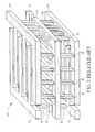
- FIG. 1 illustrates a typical MOM capacitor.
- the MOM capacitor 10 includes interdigitated multi-fingers 12 and 14 that are formed in multiple metal layers.
- the interdigitated multi-fingers are optionally connected by vias 16 and 18 in the vertical BEOL (back-end-of-line) stack separated by inter-metal dielectrics (not explicitly shown).
- BEOL back-end-of-line
- inter-metal dielectrics not explicitly shown.
- the fabricating process of an MOM capacitor can be integrated with the connect process. Hence, no extra photo mask is required.
- the dual-damascene techniques typically used with copper multilevel connection metallization on ICs can be used to construct stacks of copper-filled vias and trenches. Two or more such copper-filled vias or trenches, separated by oxide dielectrics, form an MOM capacitor.
- the entire MOM capacitor 10 is typically fabricated in back-end of line (BEOL) damascened copper layers, for example, M1 ⁇ Mn (n may typically range between 5
- HK/MG high-K/metal-gate
- an integrated capacitor includes a semiconductor substrate comprising a trench isolation area; a first interlayer dielectric (ILD) layer covering the trench isolation area; a first electrode plate comprising at least a first contact layer in the first ILD layer, wherein the contact layer is disposed directly on the trench isolation area; a second electrode plate in the first ILD layer; and a capacitor dielectric structure between the first electrode plate and the second electrode plate.
- ILD interlayer dielectric
- the first contact layer is in direct contact with the trench isolation area.
- the second electrode plate comprises a metal gate structure in the first ILD layer.
- the capacitor dielectric structure comprises a sidewall spacer on the metal gate structure.
- the capacitor dielectric structure further comprises a contact etch step layer (CESL) film.
- the capacitor dielectric structure comprises the first ILD layer.
- the integrated capacitor further includes an etch stop layer on the first ILD layer; a second ILD layer on the etch stop layer; a second contact layer stacked on the first contact layer; and a third contact layer on the metal gate structure, wherein the second and third contact layers are both in the second ILD layer.
- an integrated capacitor includes a semiconductor substrate comprising a trench isolation area; an interlayer dielectric (ILD) layer covering the trench isolation area; a first electrode plate comprising at least a contact layer in the ILD layer; a second electrode plate in the ILD layer; and a capacitor dielectric structure between the first electrode plate and the second electrode plate.
- ILD interlayer dielectric
- horizontal as used herein is defined as a plane parallel to the conventional major plane or surface of the semiconductor chip or die substrate, regardless of its orientation.
- vertical refers to a direction perpendicular to the horizontal as just defined. Terms, such as “on”, “above”, “below”, “bottom”, “top”, “side” (as in “sidewall”), "higher”, “lower”, “over”, and “under”, are defined with respect to the horizontal plane.
- Mn refers to the topmost level of the copper metal layers fabricated in the integrated circuit chip
- Mn-1 refers to the copper metal layer that is just one level lower than the topmost copper metal layer and so on, wherein, preferably, n ranges between 5 and 10 but not limited thereto.
- V refers to the via plug between two adjacent levels of conductive metal layers. For example, V5 refers to the via plug interconnecting M5 to M6, and V0 refers to the via plug interconnecting a contact layer to M1.
- front-end of line metal interconnect or "FEOL metal interconnect” refer to the metal interconnect layers including the contact layer formed during the high-K/gate-last processes, wherein the contact layer interconnects the terminals (e.g. source, drain, or gate electrode) of the transistor devices.
- back-end of line metal interconnect or “BEOL metal interconnect” refer to the metal interconnect layers formed after the high-K/gate-last processes, more specifically, after the formation of the contact layer.
- the high-K/gate-last process is known in the art.
- gate-last also known as “replacement metal gate” or "RMG” refers to that the metal electrode is deposited after the high-temperature activation anneal(s) of the flow.
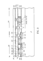
- FIGS. 2 ⁇ 4 are schematic sectional view diagrams showing an exemplary method for fabricating an MOM capacitor according to one embodiment of the invention.
- the fabrication method of the MOM capacitor can be integrated with and compatible with current high-K/gate-last processes or high-K/gate-last strain enhanced processes.
- a semiconductor substrate 10 such as a silicon substrate is provided.
- Metal gated transistor structures 20 are formed within a CMOS region 101 on the oxide define (OD) area 12.
- the OD area 12 is surrounded by or at least adjacent to a shallow trench isolation (STI) area 14.
- At least one metal gate structure 304 is provided within a capacitor forming region 102 on the STI area 14.
- the metal gated transistor structures 20 and the metal gate structure 304 are fabricated by using the same process flow.
- Each of the metal gated transistor structures 20 may comprise a metal gate layer 204, a gate dielectric layer 202 underlying the metal gate layer 204, a sidewall spacer 206, source/drain doping regions 103 in the semiconductor substrate 10, and a stressor layer 104 such as SiGe or SiC epitaxially grown on the source/drain doping region 103.
- a gate dielectric layer 302 is provided between the metal gate structure 304 and the STI area 14.
- the metal gate layer 204 may comprise metals having different work functions.
- the gate dielectric layers 202 and 302 are composed of the same high-K materials including but not limited to HfO2, HfZrO2, HfSiO4, ZrO2, ZrSiO2, TiO2, Ta2O3.
- an interfacial layer such as SiON or SiO2 may be formed before the formation of the gate dielectric layers 202 and 302.
- the sidewall spacer 206 may comprise silicon nitride or silicon oxynitride.
- the metal gated transistor structures 20 may be fabricated by using a high-K/gate-last strain enhanced process.
- a contact etch stop layer (CESL) film 106 is deposited in a blanket manner to cover the surfaces of the metal gate layer 204, the sidewall spacer 206, and the stressor layer 104 within the CMOS region 101, and cover the surfaces of the metal gate structure 304 and sidewall spacer 306 within the capacitor forming region 102.
- An inter-layer dielectric (ILD) layer 110 is then deposited on the CESL film 106.
- a polishing process such as a chemical mechanical polishing (CMP) process is carried out to remove the CESL film 106 and the ILD layer 110 from the top surface of the metal gate layer 204 and top surface of the metal gate structure 304. At this point, a planar surface is formed. The polished top surface of the ILD layer 110 is flush with the top surface of the metal gate layer 204 and the top surface of the metal gate structure 304.
- the sidewall spacers 206 and 306 are made of the same materials.
- an etch stop layer 112 is deposited on the planar surface to cover the ILD layer 110, the metal gate layer 204 and the metal gate structure 304.
- a lithographic process, an etching process, and a contact forming process are performed to form a contact layer 402 within the CMOS region 101 and a contact layer 404 within the capacitor forming region 102.
- Suitable metals for the contact layers 402 and 404 may include tungsten or alloys containing tungsten, but not limited thereto.
- the exemplary contact layer 402 penetrates through the etch stop layer 112, the ILD layer 110 and the CESL film 106 to electrically contact the stressor layer 104 and the source/drain doping layer 103.
- the contact layer 404 is in close proximity to the metal gate structure 304.
- the contact layer 404 penetrates through the etch stop layer 112, the ILD layer 110 and the CESL film 106 within the capacitor forming region 102 and may slightly recess into the STI area 14.
- an ILD layer 114 is deposited on the etch stop layer 112 and the contact layers 402 and 404.
- a lithographic process, an etching process, and a contact forming process are performed to form a contact layer 502, a contact layer 504 and contact layer 506 in the ILD layer 114.
- the contact layer 502 is aligned with the contact layer 402.
- the contact layer 504 is aligned with the contact layer 404.
- the contact layer 506 is aligned with the metal gate structure 304.
- the contact layer 506 penetrates through the etch stop layer 112 to electrically connect with the metal gate structure 304.
- at least an etch stop layer 116 and an ILD layer 118 are deposited.
- a lithographic process, an etching process, and a contact forming process are performed to form a via 602, a via 604 and via 606 in the ILD layer 118 and the etch stop layer 116.
- the via 602 is aligned with the contact layer 502.
- the via 604 is aligned with the contact layer 504.
- the via 606 is aligned with the contact layer 506.
- the via 602 is in the V0 level and is the via plug interconnecting the contact layer 502 to an interconnection wire 610 in M1 level.
- the via 602 may be formed integrally with the interconnection wire 610 in M1 level using methods known in the art, for example, copper dual damascene processes.
- a MOM capacitor 30 is completed.
- the contact layers 404, 504 constitute one electrode plate of the MOM capacitor 30.
- the contact layer 506 and the metal gate structure 304 constitute the other electrode plate of the MOM capacitor 30.
- the ILD layers 110, 114, the etch stop layer 112, the CESL film 106, and the sidewall spacer 306 constitute the capacitor dielectric of the MOM capacitor 30. Due to the two electrode plates are situated in close proximity to one another (space: ⁇ 22nm) and the relatively higher dielectric constant of the sidewall spacer 306, the MOM capacitor 30 may has increased capacitance per unit area while occupies relatively smaller amount of chip real estate.
- the fabrication of the MOM capacitor 30 is fully compatible with the current high-K/metal-gate (HK/MG) processes, particularly those high-K/gate-last processes or high-K/gate-last strain enhanced processes, and therefore no extra photo mask is required.
- HK/MG high-K/metal-gate
- the MOM capacitor 30 may be stacked by a conventional integrated capacitor formed using the BEOL metal interconnect (M1 ⁇ Mn).
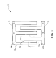
- FIG. 5 is a schematic layout diagram showing an exemplary MOM capacitor fabricated using the high-K/gate-last process based on the lithographic ground rule
- FIG. 6 is a partial cross-sectional view taken along line I-I' in FIG. 5
- the MOM capacitor 30 is composed of interdigitated first electrode vertical plates (or fingers) 30a and second electrode vertical plates (or fingers) 30b.
- a capacitor dielectric structure 30c is interposed between the first electrode vertical plate 30a and the second electrode vertical plate 30b.
- the first electrode vertical plate 30a has a first polarity and the second electrode vertical plate 30b has a second polarity opposite to the first polarity.
- the first electrode vertical plates (or fingers) 30a are electrically connected to a first connecting bar 31 where multiple vias 604 are formed.
- the second electrode vertical plates (or fingers) 30b are electrically connected to a second connecting bar 32 where multiple vias 606 are formed.
- the MOM capacitor 30 is formed on the STI area 14.
- the first electrode vertical plate 30a comprises the contact layer 404 in the ILD layer 110 and the CESL film 106, and the contact layer 504 in the ILD layer 114 and etch stop layer 112.
- the second electrode vertical plate 30b comprises the metal gate structure 304 in the ILD layer 110 and the contact layer 506 in the ILD layer 114 and etch stop layer 112.
- the capacitor dielectric structure 30c comprises the ILD layers 110 and 114, the sidewall spacer 306, the CESL film 106 and the etch stop layer 112.
- the space S1 between the contact layer 404 and the metal gate structure 304 may be equal to or smaller than 22 nm.
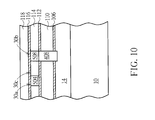
- FIGS. 7 ⁇ 10 are schematic, cross-sectional diagrams showing various MOM capacitors in accordance with different embodiments, which are all taken along line I-I' in FIG. 5 .
- the first electrode vertical plate 30a comprises only the contact layer 404 in the ILD layer 110 and the CESL film 106.
- the second electrode vertical plate 30b comprises only the metal gate structure 304 in the ILD layer 110.
- the capacitor dielectric structure 30c comprises only the ILD layer 110, the sidewall spacer 306, and the CESL film 106.
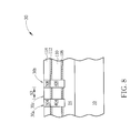
- the first electrode vertical plate 30a comprises only the contact layer 404 in the ILD layer 110 and the CESL film 106 and the contact layer 504 in the ILD layer 114 and etch stop layer 112.
- the second electrode vertical plate 30b comprises only the contact layer 408 in the ILD layer 110 and the CESL film 106 and the contact layer 508 in the ILD layer 114 and etch stop layer 112.
- the capacitor dielectric structure 30c comprises only the ILD layers 110 and 114, the etch stop layer 112, and the CESL film 106.
- the space S2 between the contact layer 404 and the contact layer 408 may be equal to or smaller than 64 nm.
- the first electrode vertical plate 30a comprises only the contact layer 504 in the ILD layer 114.
- the second electrode vertical plate 30b comprises only the contact layer 508 in the ILD layer 114.
- the capacitor dielectric structure 30c comprises only the ILD layer 114.
- the first electrode vertical plate 30a comprises only the contact layer 504 in the ILD layer 114.
- the second electrode vertical plate 30b comprises the contact layer 408 in the ILD layer 110 and the CESL film 106 and the contact layer 508 in the ILD layer 114.
- the capacitor dielectric structure 30c comprises the ILD layers 110 and 114, and the etch stop layer 112.
Landscapes
- Semiconductor Integrated Circuits (AREA)
- Internal Circuitry In Semiconductor Integrated Circuit Devices (AREA)
Abstract
Description
- The invention relates generally to the field of integrated circuits. More particularly, the invention relates to an integrated capacitor in an integrated circuit.
- Passive components such as capacitors are extensively used in integrated circuit (IC) design for radio-frequency (RF) and mixed-signal applications, such as bypassing, inter-stage coupling, and in resonant circuits and filters. One of the most commonly used capacitors is the metal-oxide-metal (MOM) capacitor.
-
FIG. 1 illustrates a typical MOM capacitor. As shown inFIG. 1 , theMOM capacitor 10 includes interdigitated multi-fingers 12 and 14 that are formed in multiple metal layers. The interdigitated multi-fingers are optionally connected byvias entire MOM capacitor 10 is typically fabricated in back-end of line (BEOL) damascened copper layers, for example, M1~Mn (n may typically range between 5~10), which are typically fabricated in extreme low-k (ELK) dielectric layers. - As devices become smaller and circuit density increases, it is desirable that capacitors maintain their level of capacitance while taking up a smaller floor area on the circuit. There is a strong need in this filed to provide such improved integrated MOM capacitor devices without adding any extra photomask.
- It is one object of the invention to provide an improved MOM capacitor structure that is compatible with current high-K/metal-gate (HK/MG) processes, particularly those high-K/gate-last processes or high-K/gate-last strain enhanced processes.
- According to one aspect of the invention, an integrated capacitor is provided. The integrated capacitor includes a semiconductor substrate comprising a trench isolation area; a first interlayer dielectric (ILD) layer covering the trench isolation area; a first electrode plate comprising at least a first contact layer in the first ILD layer, wherein the contact layer is disposed directly on the trench isolation area; a second electrode plate in the first ILD layer; and a capacitor dielectric structure between the first electrode plate and the second electrode plate.
- According to the embodiments, the first contact layer is in direct contact with the trench isolation area. According to the embodiments, the second electrode plate comprises a metal gate structure in the first ILD layer. According to the embodiments, the capacitor dielectric structure comprises a sidewall spacer on the metal gate structure. According to the embodiments, the capacitor dielectric structure further comprises a contact etch step layer (CESL) film. According to the embodiments, the capacitor dielectric structure comprises the first ILD layer.
- According to the embodiments, the integrated capacitor further includes an etch stop layer on the first ILD layer; a second ILD layer on the etch stop layer; a second contact layer stacked on the first contact layer; and a third contact layer on the metal gate structure, wherein the second and third contact layers are both in the second ILD layer.
- According to one aspect of the invention, an integrated capacitor includes a semiconductor substrate comprising a trench isolation area; an interlayer dielectric (ILD) layer covering the trench isolation area; a first electrode plate comprising at least a contact layer in the ILD layer; a second electrode plate in the ILD layer; and a capacitor dielectric structure between the first electrode plate and the second electrode plate.
- These and other objectives of the present invention will no doubt become obvious to those of ordinary skill in the art after reading the following detailed description of the preferred embodiment that is illustrated in the various figures and drawings.
- The accompanying drawings are included to provide a further understanding of the invention, and are incorporated in and constitute a part of this specification. The drawings illustrate embodiments of the invention and, together with the description, serve to explain the principles of the invention. In the drawings:
-
FIG. 1 illustrates a typical MOM capacitor; -
FIGS. 2~4 are schematic sectional view diagrams showing an exemplary method for fabricating an MOM capacitor according to one embodiment of the invention; -
FIG. 5 is a schematic layout diagram showing an exemplary MOM capacitor fabricated using the high-K/gate-last process based on the lithographic ground rule; -
FIG. 6 is a partial cross-sectional view taken along line I-I' inFIG. 5 ; and -
FIGS. 7~10 are schematic, cross-sectional diagrams showing various MOM capacitors in accordance with different embodiments. - It should be noted that all the figures are diagrammatic. Relative dimensions and proportions of parts of the drawings are exaggerated or reduced in size, for the sake of clarity and convenience. The same reference signs are generally used to refer to corresponding or similar features in modified and different embodiments.
- One or more implementations of the present invention will now be described with reference to the attached drawings, wherein like reference numerals are used to refer to like elements throughout, and wherein the illustrated structures are not necessarily drawn to scale. The term "horizontal" as used herein is defined as a plane parallel to the conventional major plane or surface of the semiconductor chip or die substrate, regardless of its orientation. The term "vertical" refers to a direction perpendicular to the horizontal as just defined. Terms, such as "on", "above", "below", "bottom", "top", "side" (as in "sidewall"), "higher", "lower", "over", and "under", are defined with respect to the horizontal plane.
- The preferred embodiments of this invention will now be explained with the accompanying figures. Throughout the specification and drawings, the symbol "Mn" refers to the topmost level of the copper metal layers fabricated in the integrated circuit chip, while "Mn-1" refers to the copper metal layer that is just one level lower than the topmost copper metal layer and so on, wherein, preferably, n ranges between 5 and 10 but not limited thereto. The symbol "V" refers to the via plug between two adjacent levels of conductive metal layers. For example, V5 refers to the via plug interconnecting M5 to M6, and V0 refers to the via plug interconnecting a contact layer to M1.
- The term "front-end of line metal interconnect" or "FEOL metal interconnect" refer to the metal interconnect layers including the contact layer formed during the high-K/gate-last processes, wherein the contact layer interconnects the terminals (e.g. source, drain, or gate electrode) of the transistor devices. The term "back-end of line metal interconnect" or "BEOL metal interconnect" refer to the metal interconnect layers formed after the high-K/gate-last processes, more specifically, after the formation of the contact layer. The high-K/gate-last process is known in the art. The term "gate-last" (also known as "replacement metal gate" or "RMG") refers to that the metal electrode is deposited after the high-temperature activation anneal(s) of the flow.
-
FIGS. 2~4 are schematic sectional view diagrams showing an exemplary method for fabricating an MOM capacitor according to one embodiment of the invention. The fabrication method of the MOM capacitor can be integrated with and compatible with current high-K/gate-last processes or high-K/gate-last strain enhanced processes. First, as shown inFIG. 2 , asemiconductor substrate 10 such as a silicon substrate is provided. Metal gatedtransistor structures 20 are formed within aCMOS region 101 on the oxide define (OD)area 12. TheOD area 12 is surrounded by or at least adjacent to a shallow trench isolation (STI)area 14. At least onemetal gate structure 304 is provided within acapacitor forming region 102 on theSTI area 14. The metal gatedtransistor structures 20 and themetal gate structure 304 are fabricated by using the same process flow. Each of the metalgated transistor structures 20 may comprise ametal gate layer 204, a gatedielectric layer 202 underlying themetal gate layer 204, asidewall spacer 206, source/drain doping regions 103 in thesemiconductor substrate 10, and astressor layer 104 such as SiGe or SiC epitaxially grown on the source/drain doping region 103. A gatedielectric layer 302 is provided between themetal gate structure 304 and theSTI area 14. Themetal gate layer 204 may comprise metals having different work functions. According to the embodiment, the gatedielectric layers dielectric layers sidewall spacer 206 may comprise silicon nitride or silicon oxynitride. - As previously mentioned, the metal gated
transistor structures 20 may be fabricated by using a high-K/gate-last strain enhanced process. Subsequently, a contact etch stop layer (CESL)film 106 is deposited in a blanket manner to cover the surfaces of themetal gate layer 204, thesidewall spacer 206, and thestressor layer 104 within theCMOS region 101, and cover the surfaces of themetal gate structure 304 andsidewall spacer 306 within thecapacitor forming region 102. An inter-layer dielectric (ILD)layer 110 is then deposited on theCESL film 106. A polishing process such as a chemical mechanical polishing (CMP) process is carried out to remove theCESL film 106 and theILD layer 110 from the top surface of themetal gate layer 204 and top surface of themetal gate structure 304. At this point, a planar surface is formed. The polished top surface of theILD layer 110 is flush with the top surface of themetal gate layer 204 and the top surface of themetal gate structure 304. Thesidewall spacers - Subsequently, an
etch stop layer 112 is deposited on the planar surface to cover theILD layer 110, themetal gate layer 204 and themetal gate structure 304. A lithographic process, an etching process, and a contact forming process are performed to form acontact layer 402 within theCMOS region 101 and acontact layer 404 within thecapacitor forming region 102. Suitable metals for the contact layers 402 and 404 may include tungsten or alloys containing tungsten, but not limited thereto. Theexemplary contact layer 402 penetrates through theetch stop layer 112, theILD layer 110 and theCESL film 106 to electrically contact thestressor layer 104 and the source/drain doping layer 103. Thecontact layer 404 is in close proximity to themetal gate structure 304. Thecontact layer 404 penetrates through theetch stop layer 112, theILD layer 110 and theCESL film 106 within thecapacitor forming region 102 and may slightly recess into theSTI area 14. - As shown in
FIG. 3 , anILD layer 114 is deposited on theetch stop layer 112 and the contact layers 402 and 404. A lithographic process, an etching process, and a contact forming process are performed to form acontact layer 502, acontact layer 504 andcontact layer 506 in theILD layer 114. Thecontact layer 502 is aligned with thecontact layer 402. Thecontact layer 504 is aligned with thecontact layer 404. Thecontact layer 506 is aligned with themetal gate structure 304. Thecontact layer 506 penetrates through theetch stop layer 112 to electrically connect with themetal gate structure 304. Subsequently, at least anetch stop layer 116 and anILD layer 118 are deposited. - As shown in
FIG. 4 , a lithographic process, an etching process, and a contact forming process are performed to form a via 602, a via 604 and via 606 in theILD layer 118 and theetch stop layer 116. The via 602 is aligned with thecontact layer 502. The via 604 is aligned with thecontact layer 504. The via 606 is aligned with thecontact layer 506. The via 602 is in the V0 level and is the via plug interconnecting thecontact layer 502 to aninterconnection wire 610 in M1 level. The via 602 may be formed integrally with theinterconnection wire 610 in M1 level using methods known in the art, for example, copper dual damascene processes. AMOM capacitor 30 is completed. - According to the embodiment, the contact layers 404, 504 constitute one electrode plate of the
MOM capacitor 30. Thecontact layer 506 and themetal gate structure 304 constitute the other electrode plate of theMOM capacitor 30. The ILD layers 110, 114, theetch stop layer 112, theCESL film 106, and thesidewall spacer 306 constitute the capacitor dielectric of theMOM capacitor 30. Due to the two electrode plates are situated in close proximity to one another (space: ~22nm) and the relatively higher dielectric constant of thesidewall spacer 306, theMOM capacitor 30 may has increased capacitance per unit area while occupies relatively smaller amount of chip real estate. - Further, as described through
FIGS. 2~4 , the fabrication of theMOM capacitor 30 is fully compatible with the current high-K/metal-gate (HK/MG) processes, particularly those high-K/gate-last processes or high-K/gate-last strain enhanced processes, and therefore no extra photo mask is required. Although not shown inFIG. 4 , it is to be understood that theMOM capacitor 30 may be stacked by a conventional integrated capacitor formed using the BEOL metal interconnect (M1~Mn). - Please refer to
FIGS. 5 andFIG. 6 , wherein like numeral numbers designate like layers, elements, or regions.FIG. 5 is a schematic layout diagram showing an exemplary MOM capacitor fabricated using the high-K/gate-last process based on the lithographic ground rule, andFIG. 6 is a partial cross-sectional view taken along line I-I' inFIG. 5 . As shown inFIG. 5 andFIG. 6 , theMOM capacitor 30 is composed of interdigitated first electrode vertical plates (or fingers) 30a and second electrode vertical plates (or fingers) 30b. Acapacitor dielectric structure 30c is interposed between the first electrodevertical plate 30a and the second electrodevertical plate 30b. The first electrodevertical plate 30a has a first polarity and the second electrodevertical plate 30b has a second polarity opposite to the first polarity. The first electrode vertical plates (or fingers) 30a are electrically connected to a first connectingbar 31 wheremultiple vias 604 are formed. The second electrode vertical plates (or fingers) 30b are electrically connected to a second connectingbar 32 wheremultiple vias 606 are formed. - As previously mentioned, the
MOM capacitor 30 is formed on theSTI area 14. The first electrodevertical plate 30a comprises thecontact layer 404 in theILD layer 110 and theCESL film 106, and thecontact layer 504 in theILD layer 114 andetch stop layer 112. The second electrodevertical plate 30b comprises themetal gate structure 304 in theILD layer 110 and thecontact layer 506 in theILD layer 114 andetch stop layer 112. Thecapacitor dielectric structure 30c comprises the ILD layers 110 and 114, thesidewall spacer 306, theCESL film 106 and theetch stop layer 112. The space S1 between thecontact layer 404 and themetal gate structure 304 may be equal to or smaller than 22 nm. -
FIGS. 7~10 are schematic, cross-sectional diagrams showing various MOM capacitors in accordance with different embodiments, which are all taken along line I-I' inFIG. 5 . As shown inFIG. 7 , the first electrodevertical plate 30a comprises only thecontact layer 404 in theILD layer 110 and theCESL film 106. The second electrodevertical plate 30b comprises only themetal gate structure 304 in theILD layer 110. Thecapacitor dielectric structure 30c comprises only theILD layer 110, thesidewall spacer 306, and theCESL film 106. - As shown in
FIG. 8 , the first electrodevertical plate 30a comprises only thecontact layer 404 in theILD layer 110 and theCESL film 106 and thecontact layer 504 in theILD layer 114 andetch stop layer 112. The second electrodevertical plate 30b comprises only thecontact layer 408 in theILD layer 110 and theCESL film 106 and thecontact layer 508 in theILD layer 114 andetch stop layer 112. Thecapacitor dielectric structure 30c comprises only the ILD layers 110 and 114, theetch stop layer 112, and theCESL film 106. The space S2 between thecontact layer 404 and thecontact layer 408 may be equal to or smaller than 64 nm. - As shown in
FIG. 9 , the first electrodevertical plate 30a comprises only thecontact layer 504 in theILD layer 114. The second electrodevertical plate 30b comprises only thecontact layer 508 in theILD layer 114. Thecapacitor dielectric structure 30c comprises only theILD layer 114. - As shown in
FIG. 10 , the first electrodevertical plate 30a comprises only thecontact layer 504 in theILD layer 114. The second electrodevertical plate 30b comprises thecontact layer 408 in theILD layer 110 and theCESL film 106 and thecontact layer 508 in theILD layer 114. Thecapacitor dielectric structure 30c comprises the ILD layers 110 and 114, and theetch stop layer 112. - Those skilled in the art will readily observe that numerous modifications and alterations of the device and method may be made while retaining the teachings of the invention. Accordingly, the above disclosure should be construed as limited only by the metes and bounds of the appended claims.
Claims (8)
- An integrated capacitor, comprising:a semiconductor substrate comprising a trench isolation area;a first interlayer dielectric (ILD) layer covering the trench isolation area;a first electrode plate comprising at least a first contact layer in the first ILD layer, wherein the contact layer is disposed directly on the trench isolation area;a second electrode plate in the first ILD layer; anda capacitor dielectric structure between the first electrode plate and the second electrode plate.
- The integrated capacitor according to claim 1 wherein the first contact layer is in direct contact with the trench isolation area.
- The integrated capacitor according to claim 2 wherein the second electrode plate comprises a metal gate structure in the first ILD layer.
- The integrated capacitor according to claim 3 wherein the capacitor dielectric structure comprises a sidewall spacer on the metal gate structure.
- The integrated capacitor according to claim 4 wherein the capacitor dielectric structure further comprises a contact etch step layer (CESL) film.
- The integrated capacitor according to claim 1 wherein the capacitor dielectric structure comprises the first ILD layer.
- The integrated capacitor according to claim 3 further comprising:an etch stop layer on the first ILD layer;a second ILD layer on the etch stop layer;a second contact layer stacked on the first contact layer; anda third contact layer on the metal gate structure, wherein the second and third contact layers are both in the second ILD layer.
- An integrated capacitor, comprising:a semiconductor substrate comprising a trench isolation area;an interlayer dielectric (ILD) layer covering the trench isolation area;a first electrode plate comprising at least a contact layer in the ILD layer;a second electrode plate in the ILD layer; anda capacitor dielectric structure between the first electrode plate and the second electrode plate.
Applications Claiming Priority (1)
| Application Number | Priority Date | Filing Date | Title |
|---|---|---|---|
| US14/337,216 US20160027772A1 (en) | 2014-07-22 | 2014-07-22 | Integrated capacitor in an integrated circuit |
Publications (2)
| Publication Number | Publication Date |
|---|---|
| EP2991109A2 true EP2991109A2 (en) | 2016-03-02 |
| EP2991109A3 EP2991109A3 (en) | 2016-03-23 |
Family
ID=52021116
Family Applications (1)
| Application Number | Title | Priority Date | Filing Date |
|---|---|---|---|
| EP14197607.6A Withdrawn EP2991109A3 (en) | 2014-07-22 | 2014-12-12 | Integrated capacitor in an integrated circuit |
Country Status (3)
| Country | Link |
|---|---|
| US (1) | US20160027772A1 (en) |
| EP (1) | EP2991109A3 (en) |
| CN (1) | CN105280607A (en) |
Families Citing this family (1)
| Publication number | Priority date | Publication date | Assignee | Title |
|---|---|---|---|---|
| CN118972536A (en) * | 2016-10-12 | 2024-11-15 | 弗劳恩霍夫应用研究促进协会 | Spatial inequality streaming |
Citations (1)
| Publication number | Priority date | Publication date | Assignee | Title |
|---|---|---|---|---|
| WO2014137589A1 (en) * | 2013-03-05 | 2014-09-12 | Qualcomm Incorporated | A metal-oxide-metal (mom) capacitor with enhanced capacitance |
Family Cites Families (6)
| Publication number | Priority date | Publication date | Assignee | Title |
|---|---|---|---|---|
| US6046103A (en) * | 1999-08-02 | 2000-04-04 | Taiwan Semiconductor Manufacturing Company | Borderless contact process for a salicide devices |
| US20080116496A1 (en) * | 2006-11-21 | 2008-05-22 | Kuo-Chyuan Tzeng | Integrating a DRAM with an SRAM having butted contacts and resulting devices |
| US8022458B2 (en) * | 2007-10-08 | 2011-09-20 | Taiwan Semiconductor Manufacturing Company, Ltd. | Capacitors integrated with metal gate formation |
| US8963223B2 (en) * | 2010-03-01 | 2015-02-24 | Broadcom Corporation | Scalable integrated MIM capacitor using gate metal |
| US8569129B2 (en) * | 2011-05-31 | 2013-10-29 | Taiwan Semiconductor Manufacturing Company, Ltd. | Device-manufacturing scheme for increasing the density of metal patterns in inter-layer dielectrics |
| US9105490B2 (en) * | 2012-09-27 | 2015-08-11 | Taiwan Semiconductor Manufacturing Company, Ltd. | Contact structure of semiconductor device |
-
2014
- 2014-07-22 US US14/337,216 patent/US20160027772A1/en not_active Abandoned
- 2014-12-12 CN CN201410767297.4A patent/CN105280607A/en active Pending
- 2014-12-12 EP EP14197607.6A patent/EP2991109A3/en not_active Withdrawn
Patent Citations (1)
| Publication number | Priority date | Publication date | Assignee | Title |
|---|---|---|---|---|
| WO2014137589A1 (en) * | 2013-03-05 | 2014-09-12 | Qualcomm Incorporated | A metal-oxide-metal (mom) capacitor with enhanced capacitance |
Also Published As
| Publication number | Publication date |
|---|---|
| US20160027772A1 (en) | 2016-01-28 |
| EP2991109A3 (en) | 2016-03-23 |
| CN105280607A (en) | 2016-01-27 |
Similar Documents
| Publication | Publication Date | Title |
|---|---|---|
| US11728375B2 (en) | Metal-insulator-metal (MIM) capacitor structure | |
| KR102404490B1 (en) | Backside capacitor techniques | |
| US8759193B2 (en) | Method of fabricating semiconductor device | |
| US8872248B2 (en) | Capacitors comprising slot contact plugs | |
| US8592945B2 (en) | Large dimension device and method of manufacturing same in gate last process | |
| US20180096936A1 (en) | Dielectric Film For Semiconductor Fabrication | |
| US20250347651A1 (en) | Semiconductor device and manufacturing method thereof | |
| KR20230076078A (en) | Guard ring structure | |
| US9190326B2 (en) | Semiconductor device having a post feature and method of manufacturing the same | |
| US20240258439A1 (en) | Schottky diode and method of fabrication thereof | |
| US11705393B2 (en) | Semiconductor device extension insulation | |
| US9601373B2 (en) | Semiconductor device and method for manufacturing the same | |
| US20160027772A1 (en) | Integrated capacitor in an integrated circuit | |
| US11282744B2 (en) | Enhanced intermetal dielectric adhesion | |
| US20250253235A1 (en) | Semiconductor device and manufacturing method thereof | |
| US20250125252A1 (en) | Semiconductor device and manufacturing method thereof | |
| US20250246535A1 (en) | Semiconductor structure | |
| US20260104383A1 (en) | Semiconductor device and manufacturing method thereof | |
| CN121001389A (en) | High-density stacked capacitors and methods |
Legal Events
| Date | Code | Title | Description |
|---|---|---|---|
| PUAL | Search report despatched |
Free format text: ORIGINAL CODE: 0009013 |
|
| PUAI | Public reference made under article 153(3) epc to a published international application that has entered the european phase |
Free format text: ORIGINAL CODE: 0009012 |
|
| AK | Designated contracting states |
Kind code of ref document: A2 Designated state(s): AL AT BE BG CH CY CZ DE DK EE ES FI FR GB GR HR HU IE IS IT LI LT LU LV MC MK MT NL NO PL PT RO RS SE SI SK SM TR |
|
| AX | Request for extension of the european patent |
Extension state: BA ME |
|
| AK | Designated contracting states |
Kind code of ref document: A3 Designated state(s): AL AT BE BG CH CY CZ DE DK EE ES FI FR GB GR HR HU IE IS IT LI LT LU LV MC MK MT NL NO PL PT RO RS SE SI SK SM TR |
|
| AX | Request for extension of the european patent |
Extension state: BA ME |
|
| RIC1 | Information provided on ipc code assigned before grant |
Ipc: H01L 49/02 20060101ALI20160217BHEP Ipc: H01L 23/522 20060101AFI20160217BHEP Ipc: H01L 27/06 20060101ALI20160217BHEP |
|
| 17P | Request for examination filed |
Effective date: 20160829 |
|
| RBV | Designated contracting states (corrected) |
Designated state(s): AL AT BE BG CH CY CZ DE DK EE ES FI FR GB GR HR HU IE IS IT LI LT LU LV MC MK MT NL NO PL PT RO RS SE SI SK SM TR |
|
| 17Q | First examination report despatched |
Effective date: 20161215 |
|
| STAA | Information on the status of an ep patent application or granted ep patent |
Free format text: STATUS: THE APPLICATION IS DEEMED TO BE WITHDRAWN |
|
| 18D | Application deemed to be withdrawn |
Effective date: 20180703 |