EP2990843A1 - Opto-electric hybrid module - Google Patents
Opto-electric hybrid module Download PDFInfo
- Publication number
- EP2990843A1 EP2990843A1 EP14807167.3A EP14807167A EP2990843A1 EP 2990843 A1 EP2990843 A1 EP 2990843A1 EP 14807167 A EP14807167 A EP 14807167A EP 2990843 A1 EP2990843 A1 EP 2990843A1
- Authority
- EP
- European Patent Office
- Prior art keywords
- cladding layer
- over
- optical element
- core
- opto
- Prior art date
- Legal status (The legal status is an assumption and is not a legal conclusion. Google has not performed a legal analysis and makes no representation as to the accuracy of the status listed.)
- Withdrawn
Links
- 238000005253 cladding Methods 0.000 claims abstract description 102
- 230000003287 optical effect Effects 0.000 claims abstract description 96
- 229920005989 resin Polymers 0.000 claims abstract description 80
- 239000011347 resin Substances 0.000 claims abstract description 80
- 238000007789 sealing Methods 0.000 claims abstract description 43
- 230000015572 biosynthetic process Effects 0.000 description 19
- 239000007788 liquid Substances 0.000 description 18
- 239000000463 material Substances 0.000 description 16
- 238000000034 method Methods 0.000 description 14
- 238000010586 diagram Methods 0.000 description 9
- 230000002093 peripheral effect Effects 0.000 description 7
- 230000005540 biological transmission Effects 0.000 description 6
- 239000002904 solvent Substances 0.000 description 5
- 238000001035 drying Methods 0.000 description 3
- 230000004048 modification Effects 0.000 description 3
- 238000012986 modification Methods 0.000 description 3
- 238000000206 photolithography Methods 0.000 description 3
- 238000010276 construction Methods 0.000 description 2
- 230000000694 effects Effects 0.000 description 2
- 230000001788 irregular Effects 0.000 description 2
- 238000004519 manufacturing process Methods 0.000 description 2
- 239000000758 substrate Substances 0.000 description 2
- 150000008065 acid anhydrides Chemical class 0.000 description 1
- 239000000654 additive Substances 0.000 description 1
- 239000000853 adhesive Substances 0.000 description 1
- 239000003795 chemical substances by application Substances 0.000 description 1
- 238000005520 cutting process Methods 0.000 description 1
- 239000003822 epoxy resin Substances 0.000 description 1
- 239000011521 glass Substances 0.000 description 1
- 238000002347 injection Methods 0.000 description 1
- 239000007924 injection Substances 0.000 description 1
- 229910052751 metal Inorganic materials 0.000 description 1
- 239000002184 metal Substances 0.000 description 1
- 150000002739 metals Chemical class 0.000 description 1
- 239000000203 mixture Substances 0.000 description 1
- 229920000647 polyepoxide Polymers 0.000 description 1
- 238000003672 processing method Methods 0.000 description 1
- 239000010453 quartz Substances 0.000 description 1
- 229910052710 silicon Inorganic materials 0.000 description 1
- 239000010703 silicon Substances 0.000 description 1
- VYPSYNLAJGMNEJ-UHFFFAOYSA-N silicon dioxide Inorganic materials O=[Si]=O VYPSYNLAJGMNEJ-UHFFFAOYSA-N 0.000 description 1
- 229910001220 stainless steel Inorganic materials 0.000 description 1
- 239000010935 stainless steel Substances 0.000 description 1
- 229920001187 thermosetting polymer Polymers 0.000 description 1
Images




Classifications
-
- G—PHYSICS
- G02—OPTICS
- G02B—OPTICAL ELEMENTS, SYSTEMS OR APPARATUS
- G02B6/00—Light guides; Structural details of arrangements comprising light guides and other optical elements, e.g. couplings
- G02B6/24—Coupling light guides
- G02B6/42—Coupling light guides with opto-electronic elements
- G02B6/4201—Packages, e.g. shape, construction, internal or external details
- G02B6/4219—Mechanical fixtures for holding or positioning the elements relative to each other in the couplings; Alignment methods for the elements, e.g. measuring or observing methods especially used therefor
- G02B6/4236—Fixing or mounting methods of the aligned elements
- G02B6/4239—Adhesive bonding; Encapsulation with polymer material
-
- G—PHYSICS
- G02—OPTICS
- G02B—OPTICAL ELEMENTS, SYSTEMS OR APPARATUS
- G02B6/00—Light guides; Structural details of arrangements comprising light guides and other optical elements, e.g. couplings
- G02B6/24—Coupling light guides
- G02B6/42—Coupling light guides with opto-electronic elements
- G02B6/4201—Packages, e.g. shape, construction, internal or external details
- G02B6/4204—Packages, e.g. shape, construction, internal or external details the coupling comprising intermediate optical elements, e.g. lenses, holograms
- G02B6/4214—Packages, e.g. shape, construction, internal or external details the coupling comprising intermediate optical elements, e.g. lenses, holograms the intermediate optical element having redirecting reflective means, e.g. mirrors, prisms for deflecting the radiation from horizontal to down- or upward direction toward a device
-
- G—PHYSICS
- G02—OPTICS
- G02B—OPTICAL ELEMENTS, SYSTEMS OR APPARATUS
- G02B6/00—Light guides; Structural details of arrangements comprising light guides and other optical elements, e.g. couplings
- G02B6/10—Light guides; Structural details of arrangements comprising light guides and other optical elements, e.g. couplings of the optical waveguide type
- G02B6/12—Light guides; Structural details of arrangements comprising light guides and other optical elements, e.g. couplings of the optical waveguide type of the integrated circuit kind
- G02B6/12002—Three-dimensional structures
-
- G—PHYSICS
- G02—OPTICS
- G02B—OPTICAL ELEMENTS, SYSTEMS OR APPARATUS
- G02B6/00—Light guides; Structural details of arrangements comprising light guides and other optical elements, e.g. couplings
- G02B6/10—Light guides; Structural details of arrangements comprising light guides and other optical elements, e.g. couplings of the optical waveguide type
- G02B6/12—Light guides; Structural details of arrangements comprising light guides and other optical elements, e.g. couplings of the optical waveguide type of the integrated circuit kind
- G02B6/122—Basic optical elements, e.g. light-guiding paths
-
- G—PHYSICS
- G02—OPTICS
- G02B—OPTICAL ELEMENTS, SYSTEMS OR APPARATUS
- G02B6/00—Light guides; Structural details of arrangements comprising light guides and other optical elements, e.g. couplings
- G02B6/10—Light guides; Structural details of arrangements comprising light guides and other optical elements, e.g. couplings of the optical waveguide type
- G02B6/12—Light guides; Structural details of arrangements comprising light guides and other optical elements, e.g. couplings of the optical waveguide type of the integrated circuit kind
- G02B6/122—Basic optical elements, e.g. light-guiding paths
- G02B6/1221—Basic optical elements, e.g. light-guiding paths made from organic materials
-
- G—PHYSICS
- G02—OPTICS
- G02B—OPTICAL ELEMENTS, SYSTEMS OR APPARATUS
- G02B6/00—Light guides; Structural details of arrangements comprising light guides and other optical elements, e.g. couplings
- G02B6/10—Light guides; Structural details of arrangements comprising light guides and other optical elements, e.g. couplings of the optical waveguide type
- G02B6/12—Light guides; Structural details of arrangements comprising light guides and other optical elements, e.g. couplings of the optical waveguide type of the integrated circuit kind
- G02B6/13—Integrated optical circuits characterised by the manufacturing method
- G02B6/138—Integrated optical circuits characterised by the manufacturing method by using polymerisation
-
- G—PHYSICS
- G02—OPTICS
- G02B—OPTICAL ELEMENTS, SYSTEMS OR APPARATUS
- G02B6/00—Light guides; Structural details of arrangements comprising light guides and other optical elements, e.g. couplings
- G02B6/24—Coupling light guides
- G02B6/42—Coupling light guides with opto-electronic elements
- G02B6/4201—Packages, e.g. shape, construction, internal or external details
- G02B6/4274—Electrical aspects
-
- G—PHYSICS
- G02—OPTICS
- G02B—OPTICAL ELEMENTS, SYSTEMS OR APPARATUS
- G02B6/00—Light guides; Structural details of arrangements comprising light guides and other optical elements, e.g. couplings
- G02B6/10—Light guides; Structural details of arrangements comprising light guides and other optical elements, e.g. couplings of the optical waveguide type
- G02B6/12—Light guides; Structural details of arrangements comprising light guides and other optical elements, e.g. couplings of the optical waveguide type of the integrated circuit kind
- G02B2006/12083—Constructional arrangements
- G02B2006/12097—Ridge, rib or the like
Definitions
- the present invention relates to an opto-electric hybrid module which includes an optical waveguide, an electric circuit provided directly on the optical waveguide, an optical element mounted on the electric circuit and a sealing resin which seals a space defined between the optical waveguide and the optical element.
- Opto-electric hybrid modules are typically produced by: individually producing an electric circuit unit including an electric circuit provided on a surface of a substrate, and an optical waveguide including an under-cladding layer, a core and an over-cladding layer stacked in this order; bonding a back surface of the substrate of the electric circuit unit to a surface of the over-cladding layer of the optical waveguide with an adhesive agent; mounting an optical element on a portion of the electric circuit unit associated with a light reflection surface (light path deflecting surface) of the core of the optical waveguide; and sealing a space defined between the optical element and the electric circuit unit with a sealing resin for protection of the optical element.
- An opto-electric hybrid module as shown in a transverse sectional view of FIG. 10 (see, for example, PTL1) is proposed, which includes an electric circuit 4 provided directly on a surface of an over-cladding layer 13 of an optical waveguide W1 for simplification of the production method thereof.
- a sealing resin 6 is provided between an optical element 5 and the over-cladding layer 13.
- a reference character 11 designates an under-cladding layer of the optical waveguide W1
- a reference character 12 designates a core of the optical waveguide W1.
- the inventors of the present invention investigated the cause of the presence of the air bubbles 20, for example, in relation to PTL1 (and other prior arts). As a result, the inventors found that this is because the space in which the sealing resin 6 is provided between the over-cladding layer 13 and the optical element 5 has a relatively great size.
- the over-cladding layer 13 has a flat surface portion in association with an optical element mounting portion, and the electric circuit 4 is provided on the flat surface portion.
- the optical element 5 is mounted on mounting pads 4a of the electric circuit 4.
- the surface of the over-cladding layer 13 and a lower surface of the optical element 5 are spaced from each other by a distance L1 that is equal to the sum of the thickness of the electric circuit 4 and the thickness of electrodes 5a of the optical element 5.
- the distance L1 is typically 25 to 150 ⁇ m.
- the sealing resin 6 is formed by injecting a liquid resin (a material for the sealing resin) from a peripheral edge of the mounting portion by means of a liquid supplying device such as a pipette, filling the space defined between the surface of the over-cladding layer 13 and the optical element 5 with the liquid resin by a capillary phenomenon, and curing the liquid resin by heat or the like. Since the space defined between the surface of the over-cladding layer 13 and the optical element 5 has a relatively great size, the liquid resin first fills a peripheral portion and then a center portion of the space defined between the surface of the over-cladding layer 13 and the optical element 5.
- a liquid resin a material for the sealing resin
- the optical element 5 generally has a light emitting portion or a light receiving portion provided in its center portion. Therefore, light emitted from the light emitting portion or light to be received by the light receiving portion is liable to be refracted or irregularly reflected on the interfaces between the sealing resin 6 and the air bubbles 20 as described above.
- an object of the present invention to provide an opto-electric hybrid module configured so that no air bubbles are present in a sealing resin which seals a space defined between an optical waveguide and an optical element.
- an opto-electric hybrid module which includes: an optical waveguide; an electric circuit provided directly on the optical waveguide; an optical element mounted on the electric circuit; and a sealing resin which seals a space defined between the optical element and the optical waveguide; wherein the optical waveguide includes an under-cladding layer, a linear light-path core provided on a surface of the under-cladding layer as projecting from the surface of the under-cladding layer, and an over-cladding layer having a portion which covers side surfaces and a top surface of the projecting core; wherein the optical waveguide has a projecting portion; and wherein the optical element is positioned above a portion of the over-cladding layer which covers the top surface of the core, and spaced a predetermined distance from the portion of the over-cladding layer.
- the over-cladding layer has the portion which covers the side surfaces and the top surface of the core projecting from the surface of the under-cladding layer, thereby the optical waveguide has a projection in shape. Then, the optical element is positioned above the portion of the over-cladding layer which covers the top surface of the core and spaced the predetermined distance from the portion of the over-cladding layer. Therefore, a smaller space is defined between the optical element and the portion of the over-cladding layer which covers the top surface of the core.
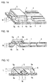
- FIGS. 1A, 1B and 1C are a perspective view, a longitudinal sectional view and a transverse sectional view, respectively, schematically illustrating an end portion (major portion) of an opto-electric hybrid module according to a first embodiment of the present invention.
- an electric circuit 4 is provided directly on an over-cladding layer 3 of an optical waveguide W, and an optical element 5 is mounted on predetermined portions (mounting pads 4a) of the electric circuit 4.
- the over-cladding layer 3 has a projection portion which covers a core 2 of the optical waveguide W, and a center portion of the optical element 5 is positioned above the projection of the over-cladding layer 3 with the intervention of a sealing resin 6.
- the optical waveguide W includes an under-cladding layer 1 having a flat surface, a linear light-path core 2 projecting from the surface of the under-cladding layer 1 and having a quadrilateral section, and an over-cladding layer 3 provided on side surfaces and a top surface of the projecting core 2 and a surface portion of the under-cladding layer 1, excluding a core formation portion, to cover the under-cladding layer 1 and the core 2.
- the over-cladding layer 3 has a flat portion covering the under-cladding layer 1, and a projection portion covering the core 2 as described above.
- the core 2 has a light reflecting surface 2a disposed below a center portion of the optical element 5 and inclined at 45 degrees with respect to an axis of the core 2.
- the light reflecting surface 2a reflects light to deflect a light path, so that the light can be transmitted between the core 2 and the optical element 5.
- the electric circuit 4 is provided on surfaces of the flat portion present on opposite sides of the projection of the over-cladding layer 3.
- the optical element 5 is mounted on the electric circuit 4 with lower end surfaces of its electrodes 5a in abutment against top surfaces of predetermined portions (mounting pads 4a) of the electric circuit 4.
- a top surface of the projection of the over-cladding layer 3 is spaced a distance L of 0.1 to 20 ⁇ m from a lower surface of the center portion of the optical element 5. No air bubbles are present in the sealing resin 6 provided between the over-cladding layer 3 and the optical element 5.
- a portion of the electric circuit 4 excluding an optical element mounting portion (mounting pads 4a) is covered with a cover-lay 7.
- the opto-electric hybrid module may be produced, for example, in the following manner.
- a flat base 10 (see FIG. 2A ) to be used for formation of an under-cladding layer 1 thereon is prepared.
- Exemplary materials for the base 10 include metals such as stainless steel, glass, quartz, silicon and resins.
- the under-cladding layer 1 is formed in a flat shape on a surface of the base 10.
- Exemplary materials for the under-cladding layer 1 include photosensitive resins and thermosetting resins.
- the formation of the under-cladding layer 1 may be achieved by a formation method suitable for the material to be used.
- the under-cladding layer 1 has a thickness of, for example, 1 to 50 ⁇ m.
- a core 2 is formed in a linear shape on a surface of the under-cladding layer 1 as projecting from the surface of the under-cladding layer 1.
- the formation of the core 2 is achieved, for example, by a photolithography method using a photosensitive resin.
- the core 2 has a height and a width of, for example, 5 to 100 ⁇ m.
- an over-cladding layer 3 (see FIG. 3C ) is formed on the surface of the under-cladding layer 1 and side surfaces and a top surface of the core 2. More specifically, a photosensitive resin having a solvent content (25 to 95 wt%) that is higher than the solvent content of a conventional photosensitive resin (0 to 20 wt%) is first prepared for the formation of the over-cladding layer. Then, as shown in FIG. 3A , the photosensitive resin is applied to a thickness slightly greater than the height of the core 2 on the surface of the under-cladding layer 1 and the surfaces of the core 2 to form a photosensitive resin layer 3a.
- the photosensitive resin layer 3a is subjected to a drying step (see FIG. 3B ), an exposure step, a PEB step (see FIG. 3C ), a developing step and a curing step in this order, whereby the over-cladding layer 3 is formed as having a projection portion which covers the core 2 and the flat portion as shown in FIG. 3C .
- a drying step and the PEB step the solvent contained in the photosensitive resin layer 3a is evaporated, so that the thickness of the photosensitive resin layer 3a is reduced.
- the thickness reduction percentage is constant throughout the photosensitive resin layer 3a.
- the over-cladding layer 3 is formed as having the projection as described above.
- the over-cladding layer 3 has a thickness (film thickness) of, for example, 1 to 50 ⁇ m. In this manner, the optical waveguide W is fabricated on the surface of the base 10.
- an electric circuit 4 is formed on flat surface portions of the over-cladding layer of the optical waveguide W on opposite sides of the projection of the over-cladding layer, for example, by a semi-additive method.
- a photosensitive insulative resin is applied onto a portion of the electric circuit 4 excluding an optical element mounting portion (mounting pads 4a) on which an optical element 5 (see FIG. 5B ) is to be mounted. Then, a cover-lay 7 is formed from the photosensitive insulative resin by a photolithography method.
- the base 10 (see FIG. 4B ) is removed from the back surface of the under-cladding layer 1, and then a predetermined portion of the core 2 is cut off from a back side of the under-cladding layer 1 by means of a cutting blade or by a laser processing method.
- a light reflecting surface 2a inclined at 45 degrees with respect to an axis of the core 2 is formed.
- a liquid resin 6a (a material for a sealing resin 6) is injected from a peripheral edge of the mounting portion by means of a liquid supplying device such as a pipette. Since a space defined between the surface of the projection of the over-cladding layer 3 and the center portion of the optical element 5 has a small size, the small space and a peripheral portion around the space are substantially simultaneously filled with the liquid resin 6a by a capillary phenomenon as shown in the transverse sectional view of FIG. 6B . After a space defined between the surface of the over-cladding layer 3 and the optical element 5 is entirely filled with the liquid resin 6a as shown in the transverse sectional view of FIG. 6C , the liquid resin 6a is cured by heat or the like to form the sealing resin 6. Thus, the opto-electric hybrid module is produced.
- the peripheral portion and the space defined between the surface of the projection of the over-cladding layer 3 and the center portion of the optical element 5 are substantially simultaneously filled with the liquid resin 6a (the material for the sealing resin 6) by the capillary phenomenon. Therefore, no air bubbles are present in the sealing resin 6 formed by curing the liquid resin 6a.
- the opto-electric hybrid module thus produced ensures proper light transmission and, hence, ensures higher light transmission efficiency without unwanted light refraction and irregular light reflection in the sealing resin 6.
- FIG. 7 is a transverse sectional view schematically illustrating an opto-electric hybrid module according to a second embodiment of the present invention.
- non-light-path dummy cores 8 not serving as light paths are provided on opposite sides of the light-path core 2 in spaced relation to the light-path core 2, and an electric circuit 4 is provided on top surfaces of the dummy cores 8.
- the over-cladding layer 3 is provided neither on the surfaces of the dummy cores 8 nor on the surface of the under-cladding layer 1, but covers the side surfaces and the top surface of the light-path core 2, whereby the optical waveguide is formed as having a projection because the over-cladding layer 3 has a portion which covers the light-path core 2.
- the second embodiment has substantially the same construction as the first embodiment except for the aforementioned arrangement, and like components are designated by like reference characters. The second embodiment provides the same effects as the first embodiment.
- the dummy cores 8 are formed from the same material as the light-path core 2 by the photolithography method when the light-path core 2 is formed.
- the dummy cores 8 may each have the same dimensions as the light-path core 2, or may each have dimensions different from those of the light-path core 2.
- the dummy cores 8 preferably each have a smaller height.
- the size of the space may be reduced by increasing the thickness of a portion of the over-cladding layer 3 present on the top surface of the light-path core 2.
- the electric circuit 4 may be formed before the formation of the over-cladding layer 3 after the formation of the light-path core 2 and the dummy cores 8. Further, the formation of the cover-lay 7 may precede the formation of the over-cladding layer 3. In this case, the portion of the electric circuit 4 excluding the mounting pads 4a may be covered with the over-cladding layer 3 rather than with the cover-lay 7. That is, when the over-cladding layer 3 is formed, the portion of the electric circuit 4 as well as the light-path core 2 may be covered with the over-cladding layer 3.
- FIG. 8 is a transverse sectional view schematically illustrating an opto-electric hybrid module according to a third embodiment of the present invention.
- the electric circuit 4 is provided on the surface of the under-cladding layer 1 on opposite sides of the light-path core 2.
- the over-cladding layer 3 is not provided on the surface of the under-cladding layer 1, but covers the side surfaces and the top surface of the light-path core 2, whereby the optical waveguide is formed as having a projection because the over-cladding layer 3 has a portion which covers the light-path core 2.
- the third embodiment has substantially the same construction as the first embodiment except for the aforementioned arrangement, and like components are designated by like reference characters.
- the third embodiment provides the same effects as the first embodiment. Particularly, the size of the space defined between the surface of the projection of the over-cladding layer 3 and the center portion of the optical element 5 can be further reduced, further suppressing the formation of air bubbles in the sealing resin 6.
- the electric circuit 4 may be formed before the formation of the core 2 after the formation of the under-cladding layer 1. Further, the formation of the cover-lay 7 may precede the formation of the core 2. In this case, the portion of the electric circuit 4 excluding the mounting pads 4a may be covered with the core 2 and/or the over-cladding layer 3 rather than with the cover-lay 7. That is, when the core 2 is formed, the portion of the electric circuit 4 may be covered with the core 2 and, when the over-cladding layer 3 is formed, a portion of the core 2 covering the portion of the electric circuit 4 may be covered with the over-cladding layer 3.
- the projection portion of the over-cladding layer 3 has a flat top surface (see FIG. 3C ), but may have a domed top surface which serves as a lens curve surface 3b as shown in a transverse sectional view of FIG. 9A .
- the top surface serves as the lens curve surface 3b
- light emitted from the light emitting portion of the optical element 5 can be converged by the action of the lens curve surface 3b and, in this state, can be transmitted to the core 2. Further, light outputted from the core 2 can be converged by the action of the lens curve surface 3b and, in this state, can be received by the light receiving portion of the optical element 5.
- the photosensitive resin layer 3a for the formation of the over-cladding layer 3 is formed as having a greater thickness than in the aforementioned embodiments (see FIG. 3A ) by applying the photosensitive resin in a greater amount for the formation of the lens curve surface 3b. That is, the formation of the thicker photosensitive resin layer 3a increases the thickness reduction amount when the thickness of the photosensitive resin layer 3a is reduced in the subsequent steps including the drying step (see FIGS. 3B and 3C ). Thus, the top surface of the projection is formed into a dome shape (lens curve surface 3b).
- An opto-electric hybrid module was produced in the same manner as in the first embodiment (see FIGS. 1A to 1C ).
- a photosensitive resin having a solvent content of 80 wt% was used as the material for the over-cladding layer.
- a mixture containing an epoxy resin and an acid anhydride curing agent in a weight ratio of 100 : 110 was used as the material for the sealing resin.
- a distance between the surface of the projection of the over-cladding layer and a lower surface of the center portion of the optical element was 15 ⁇ m.
- An opto-electric hybrid module was produced in the same manner as in the second embodiment (see FIG. 7 ).
- the material for the over-cladding layer and the material for the sealing resin were the same as those used in Example 1.
- a distance between the surface of the projection of the over-cladding layer and a lower surface of the center portion of the optical element was 10 ⁇ m.
- An opto-electric hybrid module was produced in the same manner as in the third embodiment (see FIG. 8 ).
- the material for the over-cladding layer and the material for the sealing resin were the same as those used in Example 1.
- a distance between the surface of the projection of the over-cladding layer and a lower surface of the center portion of the optical element was 5 ⁇ m.
- An opto-electric hybrid module in which an over-cladding layer had a flat surface was produced (see FIG. 10 ).
- a photosensitive resin having a solvent content of 20 wt% was used as the material for the over-cladding layer.
- the material for the sealing resin was the same as that used in Example 1.
- a distance between the surface of the over-cladding layer and a lower surface of the center portion of the optical element was 40 ⁇ m.
- the present invention is applicable to a case in which the opto-electric hybrid module is imparted with an increased light transmission efficiency for light transmission between the optical waveguide and the optical element by preventing air bubbles from being contained in the sealing resin which seals the space defined between the optical waveguide and the optical element.
Landscapes
- Physics & Mathematics (AREA)
- General Physics & Mathematics (AREA)
- Optics & Photonics (AREA)
- Engineering & Computer Science (AREA)
- Microelectronics & Electronic Packaging (AREA)
- Optical Integrated Circuits (AREA)
- Optical Couplings Of Light Guides (AREA)
- Semiconductor Lasers (AREA)
- Light Receiving Elements (AREA)
Abstract
An opto-electric hybrid module is provided, which is configured so that no air bubbles are present in a sealing resin which seals a space defined between an optical waveguide and an optical element. In the opto-electric hybrid module, an electric circuit 4 is provided directly on an over-cladding layer 3 of the optical waveguide W, and the optical element 5 is provided on predetermined portions (mounting pads 4a) of the electric circuit 4. The over-cladding layer 3 has a projection which covers a core 2, and a center portion of the optical element 5 is positioned above the projection with the intervention of a sealing resin 6.
Description
- The present invention relates to an opto-electric hybrid module which includes an optical waveguide, an electric circuit provided directly on the optical waveguide, an optical element mounted on the electric circuit and a sealing resin which seals a space defined between the optical waveguide and the optical element.
- Opto-electric hybrid modules are typically produced by: individually producing an electric circuit unit including an electric circuit provided on a surface of a substrate, and an optical waveguide including an under-cladding layer, a core and an over-cladding layer stacked in this order; bonding a back surface of the substrate of the electric circuit unit to a surface of the over-cladding layer of the optical waveguide with an adhesive agent; mounting an optical element on a portion of the electric circuit unit associated with a light reflection surface (light path deflecting surface) of the core of the optical waveguide; and sealing a space defined between the optical element and the electric circuit unit with a sealing resin for protection of the optical element.
- An opto-electric hybrid module as shown in a transverse sectional view of
FIG. 10 (see, for example, PTL1) is proposed, which includes anelectric circuit 4 provided directly on a surface of an over-claddinglayer 13 of an optical waveguide W1 for simplification of the production method thereof. In the module, asealing resin 6 is provided between anoptical element 5 and the over-claddinglayer 13. InFIG. 10 , areference character 11 designates an under-cladding layer of the optical waveguide W1, and areference character 12 designates a core of the optical waveguide W1. - PTL1:
JP-A-2007-156026 - In the prior-art opto-electric hybrid module described above, however,
air bubbles 20 are liable to be present in thesealing resin 6. In the presence of theair bubbles 20 in the sealingresin 6, light transmitted through the sealingresin 6 is refracted or irregularly reflected on interfaces between thesealing resin 6 and theair bubbles 20. This prevents the light from being properly transmitted through the sealingresin 6, thereby reducing the light transmission efficiency. - The inventors of the present invention investigated the cause of the presence of the
air bubbles 20, for example, in relation to PTL1 (and other prior arts). As a result, the inventors found that this is because the space in which the sealingresin 6 is provided between the over-claddinglayer 13 and theoptical element 5 has a relatively great size. In the prior-art opto-electric hybrid module, the over-claddinglayer 13 has a flat surface portion in association with an optical element mounting portion, and theelectric circuit 4 is provided on the flat surface portion. Theoptical element 5 is mounted onmounting pads 4a of theelectric circuit 4. Therefore, the surface of the over-claddinglayer 13 and a lower surface of theoptical element 5 are spaced from each other by a distance L1 that is equal to the sum of the thickness of theelectric circuit 4 and the thickness ofelectrodes 5a of theoptical element 5. The distance L1 is typically 25 to 150 µm. - The sealing
resin 6 is formed by injecting a liquid resin (a material for the sealing resin) from a peripheral edge of the mounting portion by means of a liquid supplying device such as a pipette, filling the space defined between the surface of the over-claddinglayer 13 and theoptical element 5 with the liquid resin by a capillary phenomenon, and curing the liquid resin by heat or the like. Since the space defined between the surface of the over-claddinglayer 13 and theoptical element 5 has a relatively great size, the liquid resin first fills a peripheral portion and then a center portion of the space defined between the surface of the over-claddinglayer 13 and theoptical element 5. Therefore, air is liable to remain in the center portion and, in this state, the liquid resin is cured, whereby the air is confined in the form ofair bubbles 20 in thesealing resin 6. Theoptical element 5 generally has a light emitting portion or a light receiving portion provided in its center portion. Therefore, light emitted from the light emitting portion or light to be received by the light receiving portion is liable to be refracted or irregularly reflected on the interfaces between thesealing resin 6 and theair bubbles 20 as described above. - In view of the foregoing, it is an object of the present invention to provide an opto-electric hybrid module configured so that no air bubbles are present in a sealing resin which seals a space defined between an optical waveguide and an optical element.
- According to the present invention to achieve the above object, there is provided an opto-electric hybrid module, which includes: an optical waveguide; an electric circuit provided directly on the optical waveguide; an optical element mounted on the electric circuit; and a sealing resin which seals a space defined between the optical element and the optical waveguide; wherein the optical waveguide includes an under-cladding layer, a linear light-path core provided on a surface of the under-cladding layer as projecting from the surface of the under-cladding layer, and an over-cladding layer having a portion which covers side surfaces and a top surface of the projecting core; wherein the optical waveguide has a projecting portion; and wherein the optical element is positioned above a portion of the over-cladding layer which covers the top surface of the core, and spaced a predetermined distance from the portion of the over-cladding layer.
- In the inventive opto-electric hybrid module, the over-cladding layer has the portion which covers the side surfaces and the top surface of the core projecting from the surface of the under-cladding layer, thereby the optical waveguide has a projection in shape. Then, the optical element is positioned above the portion of the over-cladding layer which covers the top surface of the core and spaced the predetermined distance from the portion of the over-cladding layer. Therefore, a smaller space is defined between the optical element and the portion of the over-cladding layer which covers the top surface of the core. When a liquid resin (a material for the sealing resin) is injected from a peripheral portion of an optical element mounting portion in this state, the peripheral portion of the mounting portion and the smaller space above the core are substantially simultaneously filled with the liquid resin by a capillary phenomenon. That is, the smaller space is not filled at the final stage of the liquid resin injection. Thus, the provision of the smaller space prevents air from intruding into the liquid resin present in the smaller space, so that no air bubbles are present in the liquid resin. As a result, the unwanted light refraction and irregular light reflection in the sealing resin are prevented, whereby the light can be properly transmitted through the sealing resin to increase the light transmission efficiency.
-
-
FIGS. 1A, 1B and 1C are a perspective view, a longitudinal sectional view and a transverse sectional view, respectively, schematically illustrating an opto-electric hybrid module according to a first embodiment of the present invention. -
FIG. 2A is a schematic diagram for explaining a method of forming an under-cladding layer of an optical waveguide of the opto-electric hybrid module, andFIG. 2B is a schematic diagram for explaining a method of forming a core of the optical waveguide. -
FIGS. 3A to 3C are schematic diagrams for explaining a method of forming an over-cladding layer of the optical waveguide. -
FIG. 4A is a schematic diagram for explaining a method of forming an electric circuit of the opto-electric hybrid module, andFIG. 4B is a schematic diagram for explaining a method of forming a cover-lay of the opto-electric hybrid module. -
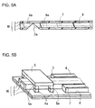
FIG. 5A is a schematic diagram for explaining a method of forming a light reflecting surface on the core, andFIG. 5B is a schematic diagram for explaining a method of mounting an optical element of the opto-electric hybrid module. -
FIGS. 6A to 6C are schematic diagrams for explaining a method of forming a sealing resin between the optical waveguide and the optical element. -
FIG. 7 is a transverse sectional view schematically illustrating an opto-electric hybrid module according to a second embodiment of the present invention. -
FIG. 8 is a transverse sectional view schematically illustrating an opto-electric hybrid module according to a third embodiment of the present invention. -
FIG. 9A is a transverse sectional view schematically showing a modification of the over-cladding layer, andFIG. 9B is a schematic diagram for explaining a method of forming the modification of the over-cladding layer. -
FIG. 10 is a transverse sectional view schematically illustrating a prior-art opto-electric hybrid module. - Embodiments of the present invention will hereinafter be described in detail based on the attached drawings.
-
FIGS. 1A, 1B and 1C are a perspective view, a longitudinal sectional view and a transverse sectional view, respectively, schematically illustrating an end portion (major portion) of an opto-electric hybrid module according to a first embodiment of the present invention. In the opto-electric hybrid module according to this embodiment, anelectric circuit 4 is provided directly on an over-claddinglayer 3 of an optical waveguide W, and anoptical element 5 is mounted on predetermined portions (mounting pads 4a) of theelectric circuit 4. The over-claddinglayer 3 has a projection portion which covers acore 2 of the optical waveguide W, and a center portion of theoptical element 5 is positioned above the projection of the over-claddinglayer 3 with the intervention of asealing resin 6. - More specifically, the optical waveguide W includes an under-
cladding layer 1 having a flat surface, a linear light-path core 2 projecting from the surface of the under-cladding layer 1 and having a quadrilateral section, and an over-claddinglayer 3 provided on side surfaces and a top surface of the projectingcore 2 and a surface portion of the under-claddinglayer 1, excluding a core formation portion, to cover the under-cladding layer 1 and thecore 2. That is, the over-claddinglayer 3 has a flat portion covering the under-cladding layer 1, and a projection portion covering thecore 2 as described above. Thecore 2 has alight reflecting surface 2a disposed below a center portion of theoptical element 5 and inclined at 45 degrees with respect to an axis of thecore 2. Thelight reflecting surface 2a reflects light to deflect a light path, so that the light can be transmitted between thecore 2 and theoptical element 5. - The
electric circuit 4 is provided on surfaces of the flat portion present on opposite sides of the projection of theover-cladding layer 3. Theoptical element 5 is mounted on theelectric circuit 4 with lower end surfaces of itselectrodes 5a in abutment against top surfaces of predetermined portions (mountingpads 4a) of theelectric circuit 4. A top surface of the projection of theover-cladding layer 3 is spaced a distance L of 0.1 to 20 µm from a lower surface of the center portion of theoptical element 5. No air bubbles are present in the sealingresin 6 provided between theover-cladding layer 3 and theoptical element 5. A portion of theelectric circuit 4 excluding an optical element mounting portion (mountingpads 4a) is covered with a cover-lay 7. - The opto-electric hybrid module may be produced, for example, in the following manner.
- First, a flat base 10 (see
FIG. 2A ) to be used for formation of an under-cladding layer 1 thereon is prepared. - Exemplary materials for the base 10 include metals such as stainless steel, glass, quartz, silicon and resins.
- Then, as shown in a perspective view of
FIG. 2A , the under-cladding layer 1 is formed in a flat shape on a surface of thebase 10. Exemplary materials for the under-cladding layer 1 include photosensitive resins and thermosetting resins. The formation of the under-cladding layer 1 may be achieved by a formation method suitable for the material to be used. The under-cladding layer 1 has a thickness of, for example, 1 to 50 µm. - Next, as shown in a perspective view of
FIG. 2B , acore 2 is formed in a linear shape on a surface of the under-cladding layer 1 as projecting from the surface of the under-cladding layer 1. The formation of thecore 2 is achieved, for example, by a photolithography method using a photosensitive resin. Thecore 2 has a height and a width of, for example, 5 to 100 µm. - Then, as shown in transverse sectional views of
FIGS. 3A to 3C , an over-cladding layer 3 (seeFIG. 3C ) is formed on the surface of the under-cladding layer 1 and side surfaces and a top surface of thecore 2. More specifically, a photosensitive resin having a solvent content (25 to 95 wt%) that is higher than the solvent content of a conventional photosensitive resin (0 to 20 wt%) is first prepared for the formation of the over-cladding layer. Then, as shown inFIG. 3A , the photosensitive resin is applied to a thickness slightly greater than the height of thecore 2 on the surface of the under-cladding layer 1 and the surfaces of thecore 2 to form aphotosensitive resin layer 3a. Thereafter, thephotosensitive resin layer 3a is subjected to a drying step (seeFIG. 3B ), an exposure step, a PEB step (seeFIG. 3C ), a developing step and a curing step in this order, whereby theover-cladding layer 3 is formed as having a projection portion which covers thecore 2 and the flat portion as shown inFIG. 3C . Particularly in the drying step and the PEB step, the solvent contained in thephotosensitive resin layer 3a is evaporated, so that the thickness of thephotosensitive resin layer 3a is reduced. The thickness reduction percentage is constant throughout thephotosensitive resin layer 3a. Therefore, a portion of thephotosensitive resin layer 3a present on the surface of the under-cladding layer 1 has a greater original thickness and correspondingly has a greater thickness reduction amount. A portion of thephotosensitive resin layer 3a present on the surfaces of thecore 2 has a smaller original thickness and correspondingly has a smaller thickness reduction amount. Thus, theover-cladding layer 3 is formed as having the projection as described above. Theover-cladding layer 3 has a thickness (film thickness) of, for example, 1 to 50 µm. In this manner, the optical waveguide W is fabricated on the surface of thebase 10. - Next, as shown in a perspective view of
FIG. 4A , anelectric circuit 4 is formed on flat surface portions of the over-cladding layer of the optical waveguide W on opposite sides of the projection of the over-cladding layer, for example, by a semi-additive method. - In turn, as shown in a perspective view of
FIG. 4B , a photosensitive insulative resin is applied onto a portion of theelectric circuit 4 excluding an optical element mounting portion (mountingpads 4a) on which an optical element 5 (seeFIG. 5B ) is to be mounted. Then, a cover-lay 7 is formed from the photosensitive insulative resin by a photolithography method. - Subsequently, as shown in a longitudinal sectional view of
FIG. 5A , the base 10 (seeFIG. 4B ) is removed from the back surface of the under-cladding layer 1, and then a predetermined portion of thecore 2 is cut off from a back side of the under-cladding layer 1 by means of a cutting blade or by a laser processing method. Thus, alight reflecting surface 2a inclined at 45 degrees with respect to an axis of thecore 2 is formed. - Then, as shown in a perspective view of
FIG. 5B , lower end surfaces ofelectrodes 5a of theoptical element 5 are brought into abutment against top surfaces of predetermined portions (mountingpads 4a) of theelectric circuit 4, whereby theoptical element 5 is mounted on theelectric circuit 4. With theoptical element 5 thus mounted, the center portion of theoptical element 5 is positioned above the projection of theover-cladding layer 3 such that a lower surface of the optical element is spaced a predetermined distance L from the projection (seeFIG. 1C ). The distance L is 0.1 to 20 µm as described above. - Thereafter, as shown in a transverse sectional view of
FIG. 6A , aliquid resin 6a (a material for a sealing resin 6) is injected from a peripheral edge of the mounting portion by means of a liquid supplying device such as a pipette. Since a space defined between the surface of the projection of theover-cladding layer 3 and the center portion of theoptical element 5 has a small size, the small space and a peripheral portion around the space are substantially simultaneously filled with theliquid resin 6a by a capillary phenomenon as shown in the transverse sectional view ofFIG. 6B . After a space defined between the surface of theover-cladding layer 3 and theoptical element 5 is entirely filled with theliquid resin 6a as shown in the transverse sectional view ofFIG. 6C , theliquid resin 6a is cured by heat or the like to form the sealingresin 6. Thus, the opto-electric hybrid module is produced. - In the production method for the opto-electric hybrid module, as described above, the peripheral portion and the space defined between the surface of the projection of the
over-cladding layer 3 and the center portion of theoptical element 5 are substantially simultaneously filled with theliquid resin 6a (the material for the sealing resin 6) by the capillary phenomenon. Therefore, no air bubbles are present in the sealingresin 6 formed by curing theliquid resin 6a. As a result, the opto-electric hybrid module thus produced ensures proper light transmission and, hence, ensures higher light transmission efficiency without unwanted light refraction and irregular light reflection in the sealingresin 6. -
FIG. 7 is a transverse sectional view schematically illustrating an opto-electric hybrid module according to a second embodiment of the present invention. In the opto-electric hybrid module according to this embodiment, non-light-path dummy cores 8 not serving as light paths are provided on opposite sides of the light-path core 2 in spaced relation to the light-path core 2, and anelectric circuit 4 is provided on top surfaces of thedummy cores 8. Theover-cladding layer 3 is provided neither on the surfaces of thedummy cores 8 nor on the surface of the under-cladding layer 1, but covers the side surfaces and the top surface of the light-path core 2, whereby the optical waveguide is formed as having a projection because theover-cladding layer 3 has a portion which covers the light-path core 2. The second embodiment has substantially the same construction as the first embodiment except for the aforementioned arrangement, and like components are designated by like reference characters. The second embodiment provides the same effects as the first embodiment. - The
dummy cores 8 are formed from the same material as the light-path core 2 by the photolithography method when the light-path core 2 is formed. Thedummy cores 8 may each have the same dimensions as the light-path core 2, or may each have dimensions different from those of the light-path core 2. In order to reduce the size of the space defined between the surface of the projection of theover-cladding layer 3 and the center portion of theoptical element 5 to suppress formation of air bubbles in the sealingresin 6, thedummy cores 8 preferably each have a smaller height. Alternatively, the size of the space may be reduced by increasing the thickness of a portion of theover-cladding layer 3 present on the top surface of the light-path core 2. - In the second embodiment, the
electric circuit 4 may be formed before the formation of theover-cladding layer 3 after the formation of the light-path core 2 and thedummy cores 8. Further, the formation of the cover-lay 7 may precede the formation of theover-cladding layer 3. In this case, the portion of theelectric circuit 4 excluding the mountingpads 4a may be covered with theover-cladding layer 3 rather than with the cover-lay 7. That is, when theover-cladding layer 3 is formed, the portion of theelectric circuit 4 as well as the light-path core 2 may be covered with theover-cladding layer 3. -
FIG. 8 is a transverse sectional view schematically illustrating an opto-electric hybrid module according to a third embodiment of the present invention. In the opto-electric hybrid module according to this embodiment, theelectric circuit 4 is provided on the surface of the under-cladding layer 1 on opposite sides of the light-path core 2. Theover-cladding layer 3 is not provided on the surface of the under-cladding layer 1, but covers the side surfaces and the top surface of the light-path core 2, whereby the optical waveguide is formed as having a projection because theover-cladding layer 3 has a portion which covers the light-path core 2. The third embodiment has substantially the same construction as the first embodiment except for the aforementioned arrangement, and like components are designated by like reference characters. The third embodiment provides the same effects as the first embodiment. Particularly, the size of the space defined between the surface of the projection of theover-cladding layer 3 and the center portion of theoptical element 5 can be further reduced, further suppressing the formation of air bubbles in the sealingresin 6. - In the third embodiment, the
electric circuit 4 may be formed before the formation of thecore 2 after the formation of the under-cladding layer 1. Further, the formation of the cover-lay 7 may precede the formation of thecore 2. In this case, the portion of theelectric circuit 4 excluding the mountingpads 4a may be covered with thecore 2 and/or theover-cladding layer 3 rather than with the cover-lay 7. That is, when thecore 2 is formed, the portion of theelectric circuit 4 may be covered with thecore 2 and, when theover-cladding layer 3 is formed, a portion of thecore 2 covering the portion of theelectric circuit 4 may be covered with theover-cladding layer 3. - In the first to third embodiments, the projection portion of the
over-cladding layer 3 has a flat top surface (seeFIG. 3C ), but may have a domed top surface which serves as alens curve surface 3b as shown in a transverse sectional view ofFIG. 9A . Where the top surface serves as thelens curve surface 3b, light emitted from the light emitting portion of theoptical element 5 can be converged by the action of thelens curve surface 3b and, in this state, can be transmitted to thecore 2. Further, light outputted from thecore 2 can be converged by the action of thelens curve surface 3b and, in this state, can be received by the light receiving portion of theoptical element 5. - As shown in a transverse sectional view of
FIG. 9B , thephotosensitive resin layer 3a for the formation of theover-cladding layer 3 is formed as having a greater thickness than in the aforementioned embodiments (seeFIG. 3A ) by applying the photosensitive resin in a greater amount for the formation of thelens curve surface 3b. That is, the formation of the thickerphotosensitive resin layer 3a increases the thickness reduction amount when the thickness of thephotosensitive resin layer 3a is reduced in the subsequent steps including the drying step (seeFIGS. 3B and 3C ). Thus, the top surface of the projection is formed into a dome shape (lens curve surface 3b). - Next, examples of the present invention will be described in conjunction with a conventional example. However, it should be understood that the present invention be not limited to the inventive examples.
- An opto-electric hybrid module was produced in the same manner as in the first embodiment (see
FIGS. 1A to 1C ). A photosensitive resin having a solvent content of 80 wt% was used as the material for the over-cladding layer. A mixture containing an epoxy resin and an acid anhydride curing agent in a weight ratio of 100 : 110 was used as the material for the sealing resin. In the opto-electric hybrid module thus produced, a distance between the surface of the projection of the over-cladding layer and a lower surface of the center portion of the optical element was 15 µm. - An opto-electric hybrid module was produced in the same manner as in the second embodiment (see
FIG. 7 ). The material for the over-cladding layer and the material for the sealing resin were the same as those used in Example 1. In the opto-electric hybrid module thus produced, a distance between the surface of the projection of the over-cladding layer and a lower surface of the center portion of the optical element was 10 µm. - An opto-electric hybrid module was produced in the same manner as in the third embodiment (see
FIG. 8 ). The material for the over-cladding layer and the material for the sealing resin were the same as those used in Example 1. In the opto-electric hybrid module thus produced, a distance between the surface of the projection of the over-cladding layer and a lower surface of the center portion of the optical element was 5 µm. - An opto-electric hybrid module in which an over-cladding layer had a flat surface was produced (see
FIG. 10 ). A photosensitive resin having a solvent content of 20 wt% was used as the material for the over-cladding layer. The material for the sealing resin was the same as that used in Example 1. In the opto-electric hybrid module thus produced, a distance between the surface of the over-cladding layer and a lower surface of the center portion of the optical element was 40 µm. - [Presence of Air Bubbles in Sealing Resin] The sealing resins of the opto-electric hybrid modules of Examples 1 to 3 and Conventional Example were each observed by means of a microscope to check whether air bubbles were present in the sealing resin. As a result, no air bubbles were present in the sealing resins in Examples 1 to 3 , but air bubbles were present in the sealing resin in Conventional Example.
- While specific forms of the embodiments of the present invention have been shown in the aforementioned inventive examples, the inventive examples are merely illustrative of the invention but not limitative of the invention. It is contemplated that various modifications apparent to those skilled in the art could be made within the scope of the invention.
- The present invention is applicable to a case in which the opto-electric hybrid module is imparted with an increased light transmission efficiency for light transmission between the optical waveguide and the optical element by preventing air bubbles from being contained in the sealing resin which seals the space defined between the optical waveguide and the optical element.
-
- W: OPTICAL WAVEGUIDE
- 2: CORE
- 3: OVER-CLADDING LAYER
- 4: ELECTRIC CIRCUIT
- 4a: MOUNTING PAD
- 5: OPTICAL ELEMENT
- 6: SEALING RESIN
Claims (1)
- An opto-electric hybrid module comprising:an optical waveguide;an electric circuit provided directly on the optical waveguide;an optical element mounted on the electric circuit; anda sealing resin which seals a space defined between the optical element and the optical waveguide;wherein the optical waveguide includes an under-cladding layer, a linear light-path core provided on a surface of the under-cladding layer as projecting from the surface of the under-cladding layer, and an over-cladding layer having a portion which covers side surfaces and a top surface of the projecting core;wherein the optical waveguide has a projecting portion; andwherein the optical element is positioned above a portion of the over-cladding layer which covers the top surface of the core, and is spaced a predetermined distance from the portion of the over-cladding layer.
Applications Claiming Priority (2)
| Application Number | Priority Date | Filing Date | Title |
|---|---|---|---|
| JP2013120846A JP2014238491A (en) | 2013-06-07 | 2013-06-07 | Opto-electric hybrid module |
| PCT/JP2014/059398 WO2014196251A1 (en) | 2013-06-07 | 2014-03-31 | Opto-electric hybrid module |
Publications (1)
| Publication Number | Publication Date |
|---|---|
| EP2990843A1 true EP2990843A1 (en) | 2016-03-02 |
Family
ID=52007906
Family Applications (1)
| Application Number | Title | Priority Date | Filing Date |
|---|---|---|---|
| EP14807167.3A Withdrawn EP2990843A1 (en) | 2013-06-07 | 2014-03-31 | Opto-electric hybrid module |
Country Status (7)
| Country | Link |
|---|---|
| US (1) | US20160116690A1 (en) |
| EP (1) | EP2990843A1 (en) |
| JP (1) | JP2014238491A (en) |
| KR (1) | KR20160016790A (en) |
| CN (1) | CN105264413A (en) |
| TW (1) | TW201447408A (en) |
| WO (1) | WO2014196251A1 (en) |
Families Citing this family (7)
| Publication number | Priority date | Publication date | Assignee | Title |
|---|---|---|---|---|
| JP6168598B2 (en) * | 2013-08-21 | 2017-07-26 | 日東電工株式会社 | Opto-electric hybrid module |
| JP7489756B2 (en) * | 2018-07-25 | 2024-05-24 | 日東電工株式会社 | Optical element device and manufacturing method thereof |
| JP7353056B2 (en) * | 2019-03-29 | 2023-09-29 | 日東電工株式会社 | Optical/electrical hybrid board with optical element |
| EP4040517A4 (en) * | 2019-09-30 | 2023-10-25 | Kyocera Corporation | HOUSING FOR OPTICAL WAVE GUIDES AND LIGHT EMITTING DEVICE |
| WO2021261427A1 (en) * | 2020-06-22 | 2021-12-30 | 日東電工株式会社 | Optical element joining-reinforcing resin composition and optical module using same |
| CN118633046A (en) * | 2022-01-31 | 2024-09-10 | 京瓷株式会社 | Optical circuit substrate |
| JP2024025173A (en) * | 2022-08-10 | 2024-02-26 | 古河電気工業株式会社 | optical waveguide structure |
Family Cites Families (20)
| Publication number | Priority date | Publication date | Assignee | Title |
|---|---|---|---|---|
| JP2000298221A (en) * | 1999-04-15 | 2000-10-24 | Sony Corp | Production of optical waveguide and production of optical transmission and receiving device |
| US20020158047A1 (en) * | 2001-04-27 | 2002-10-31 | Yiqiong Wang | Formation of an optical component having smooth sidewalls |
| JP4668049B2 (en) * | 2005-12-02 | 2011-04-13 | 京セラ株式会社 | Optical wiring module |
| US8045829B2 (en) * | 2005-12-02 | 2011-10-25 | Kyocera Corporation | Optical waveguide member, optical wiring board, optical wiring module and method for manufacturing optical waveguide member and optical wiring board |
| KR100952478B1 (en) * | 2008-02-19 | 2010-04-13 | 삼성전기주식회사 | Printed circuit board and manufacturing method thereof |
| JP4971248B2 (en) * | 2008-05-27 | 2012-07-11 | 日東電工株式会社 | Manufacturing method of opto-electric hybrid module |
| JP5071247B2 (en) * | 2008-05-30 | 2012-11-14 | 凸版印刷株式会社 | Photoelectric substrate manufacturing method |
| JP2010190994A (en) * | 2009-02-16 | 2010-09-02 | Nitto Denko Corp | Opto-electric hybrid module and method of manufacturing the same |
| JP5271141B2 (en) * | 2009-04-06 | 2013-08-21 | 日東電工株式会社 | Manufacturing method of opto-electric hybrid module and opto-electric hybrid module obtained thereby |
| JP5467826B2 (en) * | 2009-09-16 | 2014-04-09 | 日東電工株式会社 | Opto-electric hybrid module and manufacturing method thereof |
| JP5667862B2 (en) * | 2010-12-20 | 2015-02-12 | 新光電気工業株式会社 | Two-layer optical waveguide, its manufacturing method and mounting structure |
| JP2012194401A (en) * | 2011-03-16 | 2012-10-11 | Nitto Denko Corp | Opto-electric hybrid substrate and manufacturing method of the same |
| JP2012208306A (en) * | 2011-03-29 | 2012-10-25 | Nitto Denko Corp | Optoelectric hybrid substrate and manufacturing method thereof |
| JP5840988B2 (en) * | 2012-03-16 | 2016-01-06 | 日東電工株式会社 | Opto-electric hybrid board and manufacturing method thereof |
| JP5840989B2 (en) * | 2012-03-16 | 2016-01-06 | 日東電工株式会社 | Opto-electric hybrid board and manufacturing method thereof |
| JP5877749B2 (en) * | 2012-03-29 | 2016-03-08 | 日東電工株式会社 | Manufacturing method of opto-electric hybrid board |
| JP5877756B2 (en) * | 2012-05-08 | 2016-03-08 | 日東電工株式会社 | Opto-electric hybrid board and manufacturing method thereof |
| JP6045829B2 (en) * | 2012-07-13 | 2016-12-14 | 日東電工株式会社 | Opto-electric hybrid board |
| JP6202662B2 (en) * | 2012-11-27 | 2017-09-27 | 日東電工株式会社 | Opto-electric hybrid board and manufacturing method thereof |
| JP6103634B2 (en) * | 2013-02-15 | 2017-03-29 | 日東電工株式会社 | Opto-electric hybrid module |
-
2013
- 2013-06-07 JP JP2013120846A patent/JP2014238491A/en active Pending
-
2014
- 2014-03-31 US US14/895,031 patent/US20160116690A1/en not_active Abandoned
- 2014-03-31 TW TW103111971A patent/TW201447408A/en unknown
- 2014-03-31 CN CN201480029316.1A patent/CN105264413A/en active Pending
- 2014-03-31 EP EP14807167.3A patent/EP2990843A1/en not_active Withdrawn
- 2014-03-31 WO PCT/JP2014/059398 patent/WO2014196251A1/en not_active Ceased
- 2014-03-31 KR KR1020157033198A patent/KR20160016790A/en not_active Withdrawn
Non-Patent Citations (1)
| Title |
|---|
| See references of WO2014196251A1 * |
Also Published As
| Publication number | Publication date |
|---|---|
| WO2014196251A1 (en) | 2014-12-11 |
| US20160116690A1 (en) | 2016-04-28 |
| KR20160016790A (en) | 2016-02-15 |
| CN105264413A (en) | 2016-01-20 |
| JP2014238491A (en) | 2014-12-18 |
| TW201447408A (en) | 2014-12-16 |
Similar Documents
| Publication | Publication Date | Title |
|---|---|---|
| EP2990843A1 (en) | Opto-electric hybrid module | |
| US10622584B2 (en) | Display panel, packaging method thereof and OLED display apparatus | |
| US20180052273A1 (en) | Illumination apparatus confining light by total internal reflection and methods of forming the same | |
| JP2019158956A (en) | Display device | |
| US7627210B2 (en) | Manufacturing method of optical-electrical substrate and optical-electrical substrate | |
| US20230085463A1 (en) | Light-emitting device and planar light source | |
| US20110064354A1 (en) | Opto-electric hybrid module and method of manufacturing the same | |
| US8971678B2 (en) | Spacer resin pattern helping to reduce optical coupling loss in optical waveguide for light-emitting element or light-receiving element on semiconductor | |
| CN101354462A (en) | Optical waveguide device and manufacturing method thereof | |
| CN102362304A (en) | Display device and method for manufacturing the same | |
| CN101806941A (en) | Photoelectric hybrid component and its manufacturing method | |
| CN108604767A (en) | Method for manufacturing photoelectron lighting device and photoelectron lighting device | |
| TW202219424A (en) | Light emitting module and planar light source | |
| US10871605B2 (en) | Light guide plate, manufacturing method thereof and display device | |
| JP2009116008A (en) | Manufacturing method of optical waveguide device and optical waveguide device obtained thereby | |
| KR100999685B1 (en) | Optical cable module | |
| US9459419B2 (en) | Opto-electric hybrid module | |
| CN101408643B (en) | Optical waveguide device and manufacturing method thereof | |
| US20190302370A1 (en) | Optical module | |
| US9686857B2 (en) | Opto-electric hybrid module | |
| JP5280966B2 (en) | Manufacturing method of optical waveguide | |
| WO2020022428A1 (en) | Optical waveguide member connector and method therefor | |
| KR20150123198A (en) | A LED Package and A LED Package Manufacturing Method | |
| JPH02226782A (en) | Semiconductor laser device and coupling method of semiconductor laser device and optical fiber |
Legal Events
| Date | Code | Title | Description |
|---|---|---|---|
| PUAI | Public reference made under article 153(3) epc to a published international application that has entered the european phase |
Free format text: ORIGINAL CODE: 0009012 |
|
| 17P | Request for examination filed |
Effective date: 20151125 |
|
| AK | Designated contracting states |
Kind code of ref document: A1 Designated state(s): AL AT BE BG CH CY CZ DE DK EE ES FI FR GB GR HR HU IE IS IT LI LT LU LV MC MK MT NL NO PL PT RO RS SE SI SK SM TR |
|
| AX | Request for extension of the european patent |
Extension state: BA ME |
|
| STAA | Information on the status of an ep patent application or granted ep patent |
Free format text: STATUS: THE APPLICATION HAS BEEN WITHDRAWN |
|
| 18W | Application withdrawn |
Effective date: 20160422 |