EP2988418A1 - Solid-state power controller channel protection systems and methods - Google Patents
Solid-state power controller channel protection systems and methods Download PDFInfo
- Publication number
- EP2988418A1 EP2988418A1 EP15181721.0A EP15181721A EP2988418A1 EP 2988418 A1 EP2988418 A1 EP 2988418A1 EP 15181721 A EP15181721 A EP 15181721A EP 2988418 A1 EP2988418 A1 EP 2988418A1
- Authority
- EP
- European Patent Office
- Prior art keywords
- channel
- output
- state power
- power controller
- solid
- Prior art date
- Legal status (The legal status is an assumption and is not a legal conclusion. Google has not performed a legal analysis and makes no representation as to the accuracy of the status listed.)
- Granted
Links
Images



Classifications
-
- H—ELECTRICITY
- H10—SEMICONDUCTOR DEVICES; ELECTRIC SOLID-STATE DEVICES NOT OTHERWISE PROVIDED FOR
- H10D—INORGANIC ELECTRIC SEMICONDUCTOR DEVICES
- H10D89/00—Aspects of integrated devices not covered by groups H10D84/00 - H10D88/00
- H10D89/60—Integrated devices comprising arrangements for electrical or thermal protection, e.g. protection circuits against electrostatic discharge [ESD]
- H10D89/601—Integrated devices comprising arrangements for electrical or thermal protection, e.g. protection circuits against electrostatic discharge [ESD] for devices having insulated gate electrodes, e.g. for IGFETs or IGBTs
- H10D89/611—Integrated devices comprising arrangements for electrical or thermal protection, e.g. protection circuits against electrostatic discharge [ESD] for devices having insulated gate electrodes, e.g. for IGFETs or IGBTs using diodes as protective elements
-
- G—PHYSICS
- G05—CONTROLLING; REGULATING
- G05F—SYSTEMS FOR REGULATING ELECTRIC OR MAGNETIC VARIABLES
- G05F3/00—Non-retroactive systems for regulating electric variables by using an uncontrolled element, or an uncontrolled combination of elements, such element or such combination having self-regulating properties
- G05F3/02—Regulating voltage or current
- G05F3/08—Regulating voltage or current wherein the variable is DC
-
- H—ELECTRICITY
- H02—GENERATION; CONVERSION OR DISTRIBUTION OF ELECTRIC POWER
- H02H—EMERGENCY PROTECTIVE CIRCUIT ARRANGEMENTS
- H02H3/00—Emergency protective circuit arrangements for automatic disconnection directly responsive to an undesired change from normal electric working condition with or without subsequent reconnection ; integrated protection
- H02H3/08—Emergency protective circuit arrangements for automatic disconnection directly responsive to an undesired change from normal electric working condition with or without subsequent reconnection ; integrated protection responsive to excess current
-
- H—ELECTRICITY
- H02—GENERATION; CONVERSION OR DISTRIBUTION OF ELECTRIC POWER
- H02H—EMERGENCY PROTECTIVE CIRCUIT ARRANGEMENTS
- H02H3/00—Emergency protective circuit arrangements for automatic disconnection directly responsive to an undesired change from normal electric working condition with or without subsequent reconnection ; integrated protection
- H02H3/20—Emergency protective circuit arrangements for automatic disconnection directly responsive to an undesired change from normal electric working condition with or without subsequent reconnection ; integrated protection responsive to excess voltage
-
- H—ELECTRICITY
- H02—GENERATION; CONVERSION OR DISTRIBUTION OF ELECTRIC POWER
- H02J—ELECTRIC POWER NETWORKS; CIRCUIT ARRANGEMENTS OR SYSTEMS FOR SUPPLYING OR DISTRIBUTING ELECTRIC POWER; SYSTEMS FOR STORING ELECTRIC ENERGY
- H02J1/00—Circuit arrangements for DC mains or DC distribution networks
- H02J1/10—Parallel operation of DC sources
-
- H—ELECTRICITY
- H02—GENERATION; CONVERSION OR DISTRIBUTION OF ELECTRIC POWER
- H02M—APPARATUS FOR CONVERSION BETWEEN AC AND AC, BETWEEN AC AND DC, OR BETWEEN DC AND DC, AND FOR USE WITH MAINS OR SIMILAR POWER SUPPLY SYSTEMS; CONVERSION OF DC OR AC INPUT POWER INTO SURGE OUTPUT POWER; CONTROL OR REGULATION THEREOF
- H02M1/00—Details of apparatus for conversion
- H02M1/08—Circuits specially adapted for the generation of control voltages for semiconductor devices incorporated in static converters
- H02M1/088—Circuits specially adapted for the generation of control voltages for semiconductor devices incorporated in static converters for the simultaneous control of series or parallel connected semiconductor devices
-
- H—ELECTRICITY
- H02—GENERATION; CONVERSION OR DISTRIBUTION OF ELECTRIC POWER
- H02M—APPARATUS FOR CONVERSION BETWEEN AC AND AC, BETWEEN AC AND DC, OR BETWEEN DC AND DC, AND FOR USE WITH MAINS OR SIMILAR POWER SUPPLY SYSTEMS; CONVERSION OF DC OR AC INPUT POWER INTO SURGE OUTPUT POWER; CONTROL OR REGULATION THEREOF
- H02M3/00—Conversion of DC power input into DC power output
- H02M3/02—Conversion of DC power input into DC power output without intermediate conversion into AC
- H02M3/04—Conversion of DC power input into DC power output without intermediate conversion into AC by static converters
- H02M3/10—Conversion of DC power input into DC power output without intermediate conversion into AC by static converters using discharge tubes with control electrode or semiconductor devices with control electrode
- H02M3/145—Conversion of DC power input into DC power output without intermediate conversion into AC by static converters using discharge tubes with control electrode or semiconductor devices with control electrode using devices of a triode or transistor type requiring continuous application of a control signal
- H02M3/155—Conversion of DC power input into DC power output without intermediate conversion into AC by static converters using discharge tubes with control electrode or semiconductor devices with control electrode using devices of a triode or transistor type requiring continuous application of a control signal using semiconductor devices only
- H02M3/156—Conversion of DC power input into DC power output without intermediate conversion into AC by static converters using discharge tubes with control electrode or semiconductor devices with control electrode using devices of a triode or transistor type requiring continuous application of a control signal using semiconductor devices only with automatic control of output voltage or current, e.g. switching regulators
- H02M3/158—Conversion of DC power input into DC power output without intermediate conversion into AC by static converters using discharge tubes with control electrode or semiconductor devices with control electrode using devices of a triode or transistor type requiring continuous application of a control signal using semiconductor devices only with automatic control of output voltage or current, e.g. switching regulators including plural semiconductor devices as final control devices for a single load
- H02M3/1584—Conversion of DC power input into DC power output without intermediate conversion into AC by static converters using discharge tubes with control electrode or semiconductor devices with control electrode using devices of a triode or transistor type requiring continuous application of a control signal using semiconductor devices only with automatic control of output voltage or current, e.g. switching regulators including plural semiconductor devices as final control devices for a single load with a plurality of power processing stages connected in parallel
-
- H—ELECTRICITY
- H03—ELECTRONIC CIRCUITRY
- H03K—PULSE TECHNIQUE
- H03K17/00—Electronic switching or gating, i.e. not by contact-making and –breaking
- H03K17/08—Modifications for protecting switching circuit against overcurrent or overvoltage
- H03K17/082—Modifications for protecting switching circuit against overcurrent or overvoltage by feedback from the output to the control circuit
- H03K17/0822—Modifications for protecting switching circuit against overcurrent or overvoltage by feedback from the output to the control circuit in field-effect transistor switches
-
- H—ELECTRICITY
- H03—ELECTRONIC CIRCUITRY
- H03K—PULSE TECHNIQUE
- H03K17/00—Electronic switching or gating, i.e. not by contact-making and –breaking
- H03K17/12—Modifications for increasing the maximum permissible switched current
- H03K17/122—Modifications for increasing the maximum permissible switched current in field-effect transistor switches
-
- H—ELECTRICITY
- H03—ELECTRONIC CIRCUITRY
- H03K—PULSE TECHNIQUE
- H03K17/00—Electronic switching or gating, i.e. not by contact-making and –breaking
- H03K17/16—Modifications for eliminating interference voltages or currents
- H03K17/161—Modifications for eliminating interference voltages or currents in field-effect transistor switches
- H03K17/165—Modifications for eliminating interference voltages or currents in field-effect transistor switches by feedback from the output circuit to the control circuit
- H03K17/166—Soft switching
- H03K17/167—Soft switching using parallel switching arrangements
-
- H—ELECTRICITY
- H02—GENERATION; CONVERSION OR DISTRIBUTION OF ELECTRIC POWER
- H02J—ELECTRIC POWER NETWORKS; CIRCUIT ARRANGEMENTS OR SYSTEMS FOR SUPPLYING OR DISTRIBUTING ELECTRIC POWER; SYSTEMS FOR STORING ELECTRIC ENERGY
- H02J1/00—Circuit arrangements for DC mains or DC distribution networks
- H02J1/08—Three-wire DC power distribution systems; Systems having more than three wires
-
- H—ELECTRICITY
- H02—GENERATION; CONVERSION OR DISTRIBUTION OF ELECTRIC POWER
- H02J—ELECTRIC POWER NETWORKS; CIRCUIT ARRANGEMENTS OR SYSTEMS FOR SUPPLYING OR DISTRIBUTING ELECTRIC POWER; SYSTEMS FOR STORING ELECTRIC ENERGY
- H02J2105/00—Networks for supplying or distributing electric power characterised by their spatial reach or by the load
- H02J2105/30—Networks for supplying or distributing electric power characterised by their spatial reach or by the load the load networks being external to vehicles, i.e. exchanging power with vehicles
- H02J2105/32—Networks for supplying or distributing electric power characterised by their spatial reach or by the load the load networks being external to vehicles, i.e. exchanging power with vehicles for aircrafts
Definitions
- the present disclosure relates to solid-state power controllers and their components, and more particularly, to the interaction of an overload protection system and a solid-state power controller.
- Solid-state power controllers have been designed to have a current channel that can be combined with current channels of other SSPCs to achieve a desired current capacity.
- the individual channels may experience different load conditions, for example, in the event that one or more individual channel fails, or in the event that outrush current demands vary or component values vary. Some channels may become overloaded while other channels may remain within operating specifications.
- a so-called "instant trip" monitoring circuit is implemented, however, a fault may occur so rapidly that an interrupt signal from an instant trip monitoring circuit cannot reach the SSPCs in time to direct the SSPCs to trip the circuit offline before one or more channels experience an overload condition.
- a cascading trip may occur as channels are incrementally overloaded and trip offline.
- a scalable solid-state power controller system includes a power source having a channel bank including a plurality of output channels having a first output channel and a second output channel.
- the scalable solid-state power controller system includes a first solid-state power controller having a first channel current switching circuit, a second solid-state power controller having a second channel current switching circuit, a controller in electrical communication with the first solid-state power controller and the second solid-state power controller, and a combined channel output.
- the first channel current switching circuit is disposed in series between the combined channel output and the first output channel
- the second channel current switching circuit is disposed in series between the combined channel output and the second output channel.
- the first channel current switching circuit controls a first current supplied by the first output channel in response to the controller
- the second channel current switching circuit controls a second current supplied by the second output channel in response to the controller.
- a method of operating a solid-state power controller may include providing, by a controller, a control signal directing a channel current switching circuit to provide a current on a current limiter bus in response to a voltage presented on a gate control bus, and varying, by an output feedback circuit, a reactive impedance limiting the current provided to a combined channel output via the current limiter bus.
- the method may also include sensing, by the output feedback circuit, the current provided to the combined channel output, providing, by the output feedback circuit, feedback to the channel current switching circuit varying the voltage presented on the gate control bus, and maintaining the current provided to the combined channel output within a desired limit in response to the voltage presented on the gate control bus and in response to the varying the reactive impedance.
- the present disclosure relates to the design of a scalable SSPC system and, more particularly, to the design of a scalable SSPC system comprising a SSPC with self-protection features. Aspects of the designs disclosed herein may be applicable to other power supplies or power sources.
- a scalable SSPC system 10 may comprise a system whereby electrical power is provided for use by a load 4. Moreover, the scalable SSPC system 10 may condition the electrical power so that its current and voltage remains within defined boundaries and may protect itself, and/or the load 4, by preventing the current and voltage from unwanted deviations. For example, the scalable SSPC system 10 may terminate the provision of power, and/or restrict the output current in event of an unexpected drop in load 4's impedance/resistance, such as, during a short-circuit event, or in the event of another fault. For instance, the scalable SSPC system 10 may comprise one or more SSPC 3, whereby the current and or voltage presented at combined channel output 7 may be controlled.
- the scalable SSPC system 10 may comprise a power source 1, a controller 6, a SSPC 3, and a combined channel output 7.
- the power source 1 may provide electrical power via a channel 8 to one or more SSPC 3, from which it is output at combined channel output 7 in response to a control signal 5 comprising directions from controller 6 to the SSPC 3, and in response to protective actions taken by the SSPC 3 both independently and in response to the control signal 5.
- a scalable SSPC system 10 may comprise one or more SSPC 3.
- a scalable SSPC system 10 may comprise a first SSPC 3-1, a second SSPC 3-2, a third SSPC 3-3, a fourth SSPC 3-4 and/or any number of SSPCs 3.
- Each SSPC may receive electrical power via a channel 8.
- the first SSPC 3-1 may receive electrical power via a first channel 8-1
- the second SSPC 3-2 may receive electrical power via a second channel 8-2
- the third SSPC 3-3 may receive electrical power via a third channel 8-3
- the fourth SSPC 3-4 may receive electrical power via a fourth channel 8-4.
- the electrical power may be combined by the various SSPCs at combined channel output 7.
- Each SSPC may receive a corresponding control signal 5 from the controller 6.
- the first SSPC 3-1 may receive a first control signal 5-1
- the second SSPC 3-2 may receive a second control signal 5-2
- the third SSPC 3-3 may receive a third control signal 5-3
- the fourth SSPC 3-4 may receive a fourth control signal 5-4.
- the controller 6 may logically combine SSPCs to increase and/or decrease the current provided at combined channel output 7, as well as control the amount of current drawn from each channel 8.
- a power source 1 may comprise any apparatus whereby electrical power may be provided.
- the power source 1 may be a solid-state power supply.
- the power source 1 may be a linear power supply, or a switching-mode power supply, or a power supply operating according to a variety of different modes.
- the power source 1 may further comprise a generator, an alternator, a fuel cell, or another source of electrical energy and in various embodiments may be configured for aircraft use.
- the power source 1 may comprise a generator mechanically connected with a turbine engine, such as an aircraft engine or an aircraft auxiliary power unit engine.
- scalable SSPC systems 10 disclosed herein involve power sources 1 that provide direct current, in further embodiments, a power source 1 may provide an alternating current, or may provide any form of electrical power.
- the scalable SSPC system 10 may comprise a controller 6.
- the controller 6 may comprise a digital controller, an analog controller, or may comprise a combination of digital and analog components.
- the controller 6 may comprise a logical division of one or more of an aircraft data bus, a remote data concentrator, a flight computer, a full authority digital engine control (“FADEC”), an electronic engine controller (“EEC”), an engine control unit (“ECU”), and/or any other aircraft system.
- the controller 6 may comprise a processor and a tangible non-transitory memory, as well as a digital-to-analog converter (“DAC”), an analog to digital converter (“ADC”), and/or discrete logic components, for example, TTL and/or CMOS level logic devices.
- DAC digital-to-analog converter
- ADC analog to digital converter
- the controller 6 provides a control signal 5 to the SSPC 3 as discussed further herein.
- the controller 6 may provide a first control signal 5-1 to the first SSPC 3-1 a second control signal 5-2 to the second SSPC 3-2, a third control signal 5-3 to the third SSPC 3-3, a fourth control signal 5-4 to the fourth SSPC 3-4, and/or any number of control signals 5 to any number of SSPCs 3.
- the scalable SSPC system 10 may comprise one or more SSPC 3.
- a SSPC 3 may comprise analog components and/or digital components configured to limit the current and/or voltage output from the power source 1 to the combined channel output 7.
- the SSPC 3 may sense overcurrent conditions.
- the SSPCs 3 may be directed by the controller 6 to balance the total current provided at the combined channel output 7 among different channels 8 of the power source 1.
- the power source 1 may comprise a channel bank 9.
- the channel bank 9 may comprise a plurality of output channels. These channels may be combined in parallel.
- a SSPC may be associated with each channel and the controller may selectively turn different SSPCs on and off in order to logically combine channels together to provide current to the combined channel output 7. In this manner, the total current supplied by the power source 1 may be greater than the power supplied by any one channel.
- the channel bank 9 may comprise any number of channels.
- the channel bank 9 comprises two channels, or three channels, or four channels or any number of channels.
- the channel bank 9 comprises only one channel, or comprises various channels combined in various different ways.
- a channel bank 9 is illustrated in FIG. 1 , comprising four channels: Channel A 8-1, Channel B 8-2, Channel C 8-3, and Channel D 8-4. These channels may be combined in parallel by the SSPCs 3 and the aggregate current may be provided at combined channel output 7. In various embodiments, each channel may have a lesser current capacity than the combined channel output 7. In various embodiments, the SSPCs 3 are configured to maintain each channel within that channel's current capacity and to balance the current drawn among the different channels. In this manner, each channel can be maintained within its limits, even if the combined channel output 7 is of a significantly greater magnitude than an individual channel's limit.
- FIG. 1 shows a channel bank 9 having four channels 8-1, 8-2, 8-3, and 8-4, this grouping is for example only and any number of channels 8 and/or channel banks 9 may be combined, depending on the characteristics of the output power desired.
- a channel bank may comprise a single channel, for example, in the event that a single channel can provide the current desired at combined channel output 7.
- a SSPC 3 comprises a channel current switching circuit 33, an output feedback circuit 34, and a control circuit 32. These various components are connected in electrical communication.
- a channel current switching circuit 33 is connected to a channel 8.
- Channel A 8-1, Channel B 8-2, Channel C 8-3, and Channel D 8-4 each are connected to the channel current switching circuit 33 of a separate first SSPC 3-1, second SSPC 3-2, third SSPC 3-3, and fourth SSPC 3-4.
- the channel current switching circuit 33 regulates the current flowing from the connected channel, in response to the control circuit 32 and the output feedback circuit 34. The current then passes through the output feedback circuit 34 and out via the combined channel output 7 to a load 4 (see FIG. 1 ).
- An output feedback circuit 34 is connected to the channel current switching circuit 33 and the control circuit 32.
- the output feedback circuit 34 monitors the current passing out of the SSPC 3 to the combined channel output 7 and provides a signal to the control circuit 32 in response to the current passing out of the SSPC 3.
- the output feedback circuit 34 may provide a signal indicating that the control circuit 32 should direct the channel current switching circuit 33 to reduce and/or limit the current provided to the combined channel output 7 from the SSPC 3 in response to the output feedback circuit 34 detecting that the current is too high and/or is approaching a desired limit.
- the output feedback circuit 34 may provide a signal to the control circuit 32 indicating that the channel current switching circuit 33 should increase the path resistance between the channel 8 and the combined channel output 7 in order to prevent the combined current from all SSPCs 3, and/or the individual current from a single SSPC 3 from becoming too high, or reduce the path resistance to prevent the combined current from all SSPCs 3, and/or the individual current from a single SSPC 3 from becoming too low.
- the output feedback circuit 34 may contain reactive passive components, for example, to immediately respond to various circuit conditions, for example, inductive components whereby the deleterious effects of an excessive outrush current may immediately be compensated.
- a control circuit 32 may receive a control signal 5 from a controller 6 and may receive a voltage reference 31.
- the voltage reference 31 may correspond to the nominal voltage presented at the channel 8, although it may be any desired value.
- the control circuit 32 may adjust the current drawn from the channel 8 in response to the control signal 5 and the voltage reference 31.
- a SSPC 3 may comprise a channel current switching circuit 33, an output feedback circuit 34, and a control circuit 32.
- a channel current switching circuit 33 may comprise a circuit arranged to limit the current provided by the channel 8.
- the channel current switching circuit 33 may comprise a current limiter bank 54.
- the current limiter bank 54 may comprise a plurality of current limiters corresponding in number to the maximum amount of current that the connected channel 8 can provide divided by the current handling capacity of each current limiter.
- the current limiter bank 54 may comprise a first current limiter 50-1, a second current limiter 50-2, a third current limiter 50-3, and a fourth current limiter 50-4, all connected in parallel.
- the channel current switching circuit 33 may optionally include an inductive damper 64.
- Each current limiter may comprise a transistor.
- the control circuit 32 and the output feedback circuit 34 may control the current limiters.
- the transistor may comprise a field-effect transistor.
- the control circuit 32 and the output feedback circuit 34 may control the current limiters by controlling the gate of each transistor. In this manner, a selectably conductive path may be controlled corresponding to each channel of the channel bank 9.
- the gate voltage of the transistor may be changed by the control circuit 32 and the output feedback circuit 34.
- the transistor gate voltage of each current limiter may be changed by the control circuit 32 and the output feedback circuit 34 in unison, for instance, the gates may all be connected to a gate control bus 52.
- each source-drain conduction path of a transistor may be connected in parallel to a channel 8, while the other end may be connected in parallel to a current limiter bus 51.
- the transistors provide overcurrent protection to the channel 8, as well as cooperating with the transistors of the channel current switching circuits 33 of other SSPCs to actively balancing the current drawn by a load among all channels 8 of the channel bank 9, as directed by the controller 6 and/or the channel current switching circuit's respective corresponding output feedback circuit 34.
- the transistors may be operated in the linear region (also known as the ohmic or Triode mode). In this manner, the resistivity of the source-drain conduction path may be varied; however, under some circuit conditions, one or more transistors may be operated in the active region, such as when maximum current is desired to be supplied.
- Each transistor may be a p-channel FET, or an n-channel FET.
- other transistors such as bipolar junction transistors ("BJTs"), whether NPN or PNP, may be implemented, or other voltage-controlled switches or other current-controlled switches may be implemented.
- the current limiter further comprises a protection resistor connected in series with the gate of each transistor.
- the current limiter bus 51 may comprise a bus connecting the current output of each current limiter of the current limiter bank 54. These outputs may be combined, and connected to the combined channel output 7, for example, via a path through the output feedback circuit 34.
- the gate control bus 52 may comprise a bus connecting the gates of the transistors of the current limiter bank 54 together. These gates may be connected together so that the gate voltage may be changed in unison across all current limiters of current limiter bank 54 (by the control circuit 32 and the output feedback circuit 34). As a result, the current provided by the combined channel output 7 may be balanced across all the channels 8 of the channel bank 9, via individualized control of each SSPC's gate control bus 52 via control signals 5.
- An inductive damper 64 may be disposed in series with the current limiter bus 51 and the combined channel output 7.
- the inductive damper 64 may comprise an inductor or any other component configured to dampen changes in current over time. In this manner, large startup currents may be dampened, protecting the load, and fluctuations/noise caused by the load, such as switching noise, may be dampened, protecting the scalable SSPC system 10.
- An output feedback circuit 34 may comprise a circuit arranged to monitor the combined current provided at the combined channel output 7 and provide feedback to the channel current switching circuit 33 instructing the channel current switching circuit 33 to increase or decrease the current provided.
- the output feedback circuit 34 may comprise a feedback amplifier 62, and a sense resistor 65.
- the output feedback circuit 34 may optionally include a signal amplifier 63.
- a feedback amplifier 62 may comprise a current controlled amplifier.
- the feedback amplifier 62 may comprise a bipolar junction transistor.
- the sense resistor 65 may comprise a resistor disposed between the channel current switching circuit 33 and the combined channel output 7. As current flows through the sense resistor 65, a voltage is developed across the sense resistor 65.
- the base of the bipolar junction transistor and the emitter of the bipolar junction transistor may be connected to opposite sides of the sense resistor 65. In this manner, the voltage developed across the sense resistor 65 controls the resistivity of the bipolar junction transistor collector-emitter pathway.
- the collector may be connected to a control circuit 32 (for example, the control circuit/feedback circuit balancer 35 discussed further herein), which may then connect to the gate control bus 52.
- the voltage present on the gate control bus 52 may be controlled in response to the current flowing through the sense resistor 65 so that a feedback loop is established wherein the feedback amplifier 62 controls the gate control bus voltage in response to the current output of the SSPC (which is then combined with that of any other SSPCs and provided to combined channel output 7).
- the gate control bus 52 voltage may change in response to the output current to cause the channel current switching circuit 33 to limit the output current and bring it into compliance with the desired current limit, such as in the event of a fault condition.
- Some fault conditions may include a short circuit or startup load variations, such as outrush current during a transient event.
- a signal amplifier 63 may be disposed between the sense resistor 65 and the base of the bipolar junction transistor comprising the feedback amplifier 62.
- the signal amplifier 63 may increase and/or decrease the sensitivity of the output feedback circuit 34, or may otherwise condition the behavior of the output feedback circuit 34 as desired for a particular application.
- the amplifier comprises a solid-state operational amplifier, though any amplifier configuration may be implemented.
- the signal amplifier 63 is omitted.
- the control circuit 32 may include a overvoltage protector 41 and a control circuit/feedback circuit balancer 35.
- the overvoltage protector 41 may be in electrical communication with a voltage reference 31.
- the overvoltage protector 41 may comprise a circuit to condition the voltage reference 31 and provide power to the gate control bus 52 during certain scenarios, such as a transient overvoltage condition, to force current limiters 50 to an on condition until the scenario, such as a transient overvoltage condition, has passed.
- the overvoltage protector 41 may provide overvoltage protection, such as lightning protection.
- the overvoltage protector 41 comprises a Zener diode 42 and a power diode 43.
- the Zener diode 42 may be arranged in a reverse biased configuration in order to regulate the voltage supplied by the overvoltage protector 41 while the power diode 43 may be arranged in a forward biased configuration in order to provide reverse current protection to voltage reference 31 and enable proper functioning of control circuit/feedback circuit balancer 35.
- the control circuit 32 may selectively sink the gate control bus 52 to ground, thus selectively changing the voltage on the gate control bus 52.
- the control circuit 32 may comprise a control circuit/feedback circuit balancer 35 comprising a voltage divider to join different signals on the gate control bus 52.
- the control signal 5 may be connected to the control circuit 32.
- a control resistor 44 may be disposed in the circuit path.
- the channel current switching circuit 33 may be connected to the control circuit 32 and a feedback resistor 61 may be disposed in the circuit path between the collector of the feedback amplifier 62 and the overvoltage protector 41. The channel current switching circuit 33 and the control signal 5 may selectively change the voltage on the gate control bus 52.
- control signal 5 may control the voltage present on gate control bus 52, however, during an overcurrent condition, the output feedback circuit 34 may lower the voltage on the gate control bus 52 and during an overcurrent condition, overvoltage protector 41 may increase the voltage on the gate control bus 52.
- a parallel voltage divider may be established by the feedback resistor 61 and the control resistor 44 which are connected in parallel (and are in series with the overvoltage protector 41).
- the gate control bus 52 may also be connected in parallel with the feedback resistor 61 and the control resistor 44.
- the voltage presented on the gate control bus 52 may be varied in response to the control signal 5, which may comprise a resistivity of the path through the controller 6, and in response to the resistivity of the collector-emitter path through the bipolar junction transistor comprising the feedback amplifier 62.
- the controller 6 may control the current supplied by the SSPC to the combined channel output 7 through the channel 8
- the output feedback circuit 34 may also control the current supplied at the combined channel output 7 through the channel 8.
- the feedback resistor 61 and control resistor 44 may be selected to enable a prioritization of the different control functions connected to gate control bus 52. For example, if overvoltage protector 41 conducts due to an overvoltage, overvoltage protector 41 has the highest priority because, among other reasons, there is no resistor between overvoltage protector 41 and the gate control bus 52. If there is no overvoltage, but there is an overcurrent, feedback resistor 61 facilitates a controlled reduction in the voltage on gate control bus 52.
- overvoltage protector 41 may override feedback resistor 61 and control resistor 44 because it provides a direct path without a resistor - thus, the current limiters 50 may be forced on, even though an overcurrent condition exists, in order to address the overvoltage condition as a higher priority condition.
- feedback resistor 61 may provide no control function and instead the control signal 5 via control resistor 44 may control the voltage on gate control bus 52.
- a SSPC 3 may be operated according to various methods.
- a method 400 is provided wherein the controller 6 may provide a control signal 5 directing a channel current switching circuit 33 to provide a current on a current limiter bus 51 in response to a voltage presented on a gate control bus 52 (Step 410).
- the load 4 may be a reactive load, so that a large outrush current is demanded at initial startup.
- the output feedback circuit 34 may vary a reactive impedance limiting the current provided to a combined channel output 7 (Step 420).
- the SSPC 3 may sense, by the output feedback circuit 34, the current provided to the combined channel output 7 (Step 430).
- the output feedback circuit 34 may provide feedback to the channel current switching circuit 33 varying the voltage presented on the gate control bus 52 (Step 440). In this manner, the current provided to the combined channel output 7 may be maintained within a desired limit in response to the voltage presented on the gate control bus 52 and in response to the varying the reactive impedance (Step 450).
- the SSPC 3 may provide active current regulation, such as in response to transient events, for example, a load fault, such as outrush currents short circuits, and/or overload conditions.
- references to "various embodiments”, “one embodiment”, “an embodiment”, “an example embodiment”, etc. indicate that the embodiment described may include a particular feature, structure, or characteristic, but every embodiment may not necessarily include the particular feature, structure, or characteristic. Moreover, such phrases are not necessarily referring to the same embodiment. Further, when a particular feature, structure, or characteristic is described in connection with an embodiment, it is submitted that it is within the knowledge of one skilled in the art to affect such feature, structure, or characteristic in connection with other embodiments whether or not explicitly described. After reading the description, it will be apparent to one skilled in the relevant art(s) how to implement the disclosure in alternative embodiments.
Landscapes
- Engineering & Computer Science (AREA)
- Power Engineering (AREA)
- Physics & Mathematics (AREA)
- Electromagnetism (AREA)
- General Physics & Mathematics (AREA)
- Radar, Positioning & Navigation (AREA)
- Automation & Control Theory (AREA)
- Emergency Protection Circuit Devices (AREA)
Abstract
Description
- The present disclosure relates to solid-state power controllers and their components, and more particularly, to the interaction of an overload protection system and a solid-state power controller.
- Solid-state power controllers ("SSPC") have been designed to have a current channel that can be combined with current channels of other SSPCs to achieve a desired current capacity. However, the individual channels may experience different load conditions, for example, in the event that one or more individual channel fails, or in the event that outrush current demands vary or component values vary. Some channels may become overloaded while other channels may remain within operating specifications. In some instances, a so-called "instant trip" monitoring circuit is implemented, however, a fault may occur so rapidly that an interrupt signal from an instant trip monitoring circuit cannot reach the SSPCs in time to direct the SSPCs to trip the circuit offline before one or more channels experience an overload condition. Moreover, in the event, that a load draws a prolonged outrush current, a cascading trip may occur as channels are incrementally overloaded and trip offline.
- A scalable solid-state power controller system is disclosed. The scalable solid-state power controller system includes a power source having a channel bank including a plurality of output channels having a first output channel and a second output channel. The scalable solid-state power controller system includes a first solid-state power controller having a first channel current switching circuit, a second solid-state power controller having a second channel current switching circuit, a controller in electrical communication with the first solid-state power controller and the second solid-state power controller, and a combined channel output. In various embodiments, the first channel current switching circuit is disposed in series between the combined channel output and the first output channel, and the second channel current switching circuit is disposed in series between the combined channel output and the second output channel. In various embodiments, the first channel current switching circuit controls a first current supplied by the first output channel in response to the controller, and the second channel current switching circuit controls a second current supplied by the second output channel in response to the controller.
- A method of operating a solid-state power controller is disclosed. The method may include providing, by a controller, a control signal directing a channel current switching circuit to provide a current on a current limiter bus in response to a voltage presented on a gate control bus, and varying, by an output feedback circuit, a reactive impedance limiting the current provided to a combined channel output via the current limiter bus. The method may also include sensing, by the output feedback circuit, the current provided to the combined channel output, providing, by the output feedback circuit, feedback to the channel current switching circuit varying the voltage presented on the gate control bus, and maintaining the current provided to the combined channel output within a desired limit in response to the voltage presented on the gate control bus and in response to the varying the reactive impedance.
- The subject matter of the present disclosure is particularly pointed out and distinctly claimed in the concluding portion of the specification. A more complete understanding of the present disclosure, however, may best be obtained by referring to the detailed description and claims when considered in connection with the drawing figures, wherein like numerals denote like elements.
-
FIG. 1 depict block diagrams of a circuit containing a scalable SSPC system having one or more SSPC in accordance with various embodiments; -
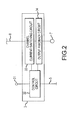
FIG. 2 depicts a block diagram of a SSPC in accordance with various embodiments; -
FIG. 3 depicts a detailed view of a SSPC in accordance with various embodiments; and -
FIG. 4 depicts a method whereby a scalable SSPC system may be operated in accordance with various embodiments. - The detailed description of exemplary embodiments herein makes reference to the accompanying drawings, which show exemplary embodiments by way of illustration and their best mode. While these exemplary embodiments are described in sufficient detail to enable those skilled in the art to practice the disclosure, it should be understood that other embodiments may be realized and that logical changes may be made without departing from the scope of the disclosure. Thus, the detailed description herein is presented for purposes of illustration only and not of limitation. For example, the steps recited in any of the method or process descriptions may be executed in any order and are not necessarily limited to the order presented. Furthermore, any reference to singular includes plural embodiments, and any reference to more than one component or step may include a singular embodiment or step.
- The present disclosure relates to the design of a scalable SSPC system and, more particularly, to the design of a scalable SSPC system comprising a SSPC with self-protection features. Aspects of the designs disclosed herein may be applicable to other power supplies or power sources.
- According to various embodiments, and with reference to
FIG. 1 , ascalable SSPC system 10 may comprise a system whereby electrical power is provided for use by aload 4. Moreover, thescalable SSPC system 10 may condition the electrical power so that its current and voltage remains within defined boundaries and may protect itself, and/or theload 4, by preventing the current and voltage from unwanted deviations. For example, thescalable SSPC system 10 may terminate the provision of power, and/or restrict the output current in event of an unexpected drop inload 4's impedance/resistance, such as, during a short-circuit event, or in the event of another fault. For instance, thescalable SSPC system 10 may comprise one ormore SSPC 3, whereby the current and or voltage presented at combined channel output 7 may be controlled. - In various embodiments, the
scalable SSPC system 10 may comprise a power source 1, a controller 6, a SSPC 3, and a combined channel output 7. The power source 1 may provide electrical power via a channel 8 to one ormore SSPC 3, from which it is output at combined channel output 7 in response to a control signal 5 comprising directions from controller 6 to theSSPC 3, and in response to protective actions taken by theSSPC 3 both independently and in response to the control signal 5. - With continuing reference to
FIG. 1 , ascalable SSPC system 10 may comprise one ormore SSPC 3. For example, ascalable SSPC system 10 may comprise a first SSPC 3-1, a second SSPC 3-2, a third SSPC 3-3, a fourth SSPC 3-4 and/or any number ofSSPCs 3. Each SSPC may receive electrical power via a channel 8. For example, the first SSPC 3-1 may receive electrical power via a first channel 8-1, the second SSPC 3-2 may receive electrical power via a second channel 8-2, the third SSPC 3-3 may receive electrical power via a third channel 8-3, and the fourth SSPC 3-4 may receive electrical power via a fourth channel 8-4. The electrical power may be combined by the various SSPCs at combined channel output 7. Each SSPC may receive a corresponding control signal 5 from the controller 6. For example, the first SSPC 3-1 may receive a first control signal 5-1, the second SSPC 3-2 may receive a second control signal 5-2, the third SSPC 3-3 may receive a third control signal 5-3, and the fourth SSPC 3-4 may receive a fourth control signal 5-4. By controlling each SSPC, the controller 6 may logically combine SSPCs to increase and/or decrease the current provided at combined channel output 7, as well as control the amount of current drawn from each channel 8. - A power source 1 may comprise any apparatus whereby electrical power may be provided. For example, the power source 1 may be a solid-state power supply. The power source 1 may be a linear power supply, or a switching-mode power supply, or a power supply operating according to a variety of different modes. The power source 1 may further comprise a generator, an alternator, a fuel cell, or another source of electrical energy and in various embodiments may be configured for aircraft use. For example, the power source 1 may comprise a generator mechanically connected with a turbine engine, such as an aircraft engine or an aircraft auxiliary power unit engine. Although,
scalable SSPC systems 10 disclosed herein involve power sources 1 that provide direct current, in further embodiments, a power source 1 may provide an alternating current, or may provide any form of electrical power. - In various embodiments, the
scalable SSPC system 10 may comprise a controller 6. The controller 6 may comprise a digital controller, an analog controller, or may comprise a combination of digital and analog components. The controller 6 may comprise a logical division of one or more of an aircraft data bus, a remote data concentrator, a flight computer, a full authority digital engine control ("FADEC"), an electronic engine controller ("EEC"), an engine control unit ("ECU"), and/or any other aircraft system. The controller 6 may comprise a processor and a tangible non-transitory memory, as well as a digital-to-analog converter ("DAC"), an analog to digital converter ("ADC"), and/or discrete logic components, for example, TTL and/or CMOS level logic devices. The controller 6 provides a control signal 5 to the SSPC 3 as discussed further herein. For example, the controller 6 may provide a first control signal 5-1 to the first SSPC 3-1 a second control signal 5-2 to the second SSPC 3-2, a third control signal 5-3 to the third SSPC 3-3, a fourth control signal 5-4 to the fourth SSPC 3-4, and/or any number of control signals 5 to any number ofSSPCs 3. - The
scalable SSPC system 10 may comprise one ormore SSPC 3. A SSPC 3 may comprise analog components and/or digital components configured to limit the current and/or voltage output from the power source 1 to the combined channel output 7. For example, the SSPC 3 may sense overcurrent conditions. Moreover, in embodiments comprising a plurality ofSSPCs 3, theSSPCs 3 may be directed by the controller 6 to balance the total current provided at the combined channel output 7 among different channels 8 of the power source 1. - Having discussed various aspects of a
scalable SSPC system 10, the power source 1 may comprise achannel bank 9. Thechannel bank 9 may comprise a plurality of output channels. These channels may be combined in parallel. For example, a SSPC may be associated with each channel and the controller may selectively turn different SSPCs on and off in order to logically combine channels together to provide current to the combined channel output 7. In this manner, the total current supplied by the power source 1 may be greater than the power supplied by any one channel. For example, thechannel bank 9 may comprise any number of channels. In various embodiments, thechannel bank 9 comprises two channels, or three channels, or four channels or any number of channels. In further embodiments, thechannel bank 9 comprises only one channel, or comprises various channels combined in various different ways. For the purpose of illustration, achannel bank 9 is illustrated inFIG. 1 , comprising four channels: Channel A 8-1, Channel B 8-2, Channel C 8-3, and Channel D 8-4. These channels may be combined in parallel by the SSPCs 3 and the aggregate current may be provided at combined channel output 7. In various embodiments, each channel may have a lesser current capacity than the combined channel output 7. In various embodiments, theSSPCs 3 are configured to maintain each channel within that channel's current capacity and to balance the current drawn among the different channels. In this manner, each channel can be maintained within its limits, even if the combined channel output 7 is of a significantly greater magnitude than an individual channel's limit. - Moreover, while
FIG. 1 shows achannel bank 9 having four channels 8-1, 8-2, 8-3, and 8-4, this grouping is for example only and any number of channels 8 and/orchannel banks 9 may be combined, depending on the characteristics of the output power desired. For further example, in various embodiments, a channel bank may comprise a single channel, for example, in the event that a single channel can provide the current desired at combined channel output 7. - Now, with reference to
FIG. 2 , aSSPC 3 is presented in greater detail. In various embodiments, aSSPC 3 comprises a channelcurrent switching circuit 33, anoutput feedback circuit 34, and acontrol circuit 32. These various components are connected in electrical communication. - A channel
current switching circuit 33 is connected to a channel 8. For example, Channel A 8-1, Channel B 8-2, Channel C 8-3, and Channel D 8-4 each are connected to the channelcurrent switching circuit 33 of a separate first SSPC 3-1, second SSPC 3-2, third SSPC 3-3, and fourth SSPC 3-4. The channelcurrent switching circuit 33 regulates the current flowing from the connected channel, in response to thecontrol circuit 32 and theoutput feedback circuit 34. The current then passes through theoutput feedback circuit 34 and out via the combined channel output 7 to a load 4 (seeFIG. 1 ). - An
output feedback circuit 34 is connected to the channelcurrent switching circuit 33 and thecontrol circuit 32. Theoutput feedback circuit 34 monitors the current passing out of theSSPC 3 to the combined channel output 7 and provides a signal to thecontrol circuit 32 in response to the current passing out of theSSPC 3. For example, theoutput feedback circuit 34 may provide a signal indicating that thecontrol circuit 32 should direct the channelcurrent switching circuit 33 to reduce and/or limit the current provided to the combined channel output 7 from theSSPC 3 in response to theoutput feedback circuit 34 detecting that the current is too high and/or is approaching a desired limit. Theoutput feedback circuit 34 may provide a signal to thecontrol circuit 32 indicating that the channelcurrent switching circuit 33 should increase the path resistance between the channel 8 and the combined channel output 7 in order to prevent the combined current from allSSPCs 3, and/or the individual current from asingle SSPC 3 from becoming too high, or reduce the path resistance to prevent the combined current from allSSPCs 3, and/or the individual current from asingle SSPC 3 from becoming too low. Moreover, theoutput feedback circuit 34 may contain reactive passive components, for example, to immediately respond to various circuit conditions, for example, inductive components whereby the deleterious effects of an excessive outrush current may immediately be compensated. - A
control circuit 32 may receive a control signal 5 from a controller 6 and may receive avoltage reference 31. In various embodiments, thevoltage reference 31 may correspond to the nominal voltage presented at the channel 8, although it may be any desired value. Thecontrol circuit 32 may adjust the current drawn from the channel 8 in response to the control signal 5 and thevoltage reference 31. - Now, with reference to
FIG. 3 , a detailed schematic diagram of anexample SSPC 3 is provided. As previously discussed, aSSPC 3 may comprise a channelcurrent switching circuit 33, anoutput feedback circuit 34, and acontrol circuit 32. - A channel
current switching circuit 33 may comprise a circuit arranged to limit the current provided by the channel 8. For instance, the channelcurrent switching circuit 33 may comprise acurrent limiter bank 54. Thecurrent limiter bank 54 may comprise a plurality of current limiters corresponding in number to the maximum amount of current that the connected channel 8 can provide divided by the current handling capacity of each current limiter. For example, thecurrent limiter bank 54 may comprise a first current limiter 50-1, a second current limiter 50-2, a third current limiter 50-3, and a fourth current limiter 50-4, all connected in parallel. Moreover, the channelcurrent switching circuit 33 may optionally include aninductive damper 64. - Each current limiter may comprise a transistor. The
control circuit 32 and theoutput feedback circuit 34 may control the current limiters. In addition, the transistor may comprise a field-effect transistor. Thus, in various embodiments, thecontrol circuit 32 and theoutput feedback circuit 34 may control the current limiters by controlling the gate of each transistor. In this manner, a selectably conductive path may be controlled corresponding to each channel of thechannel bank 9. In various embodiments, the gate voltage of the transistor may be changed by thecontrol circuit 32 and theoutput feedback circuit 34. Furthermore, in various embodiments, the transistor gate voltage of each current limiter may be changed by thecontrol circuit 32 and theoutput feedback circuit 34 in unison, for instance, the gates may all be connected to agate control bus 52. In this manner, the resistivity of the source-drain conduction path of the transistors may be varied, thus variously limiting the amount of current flowing through the transistors. One end of each source-drain conduction path of a transistor may be connected in parallel to a channel 8, while the other end may be connected in parallel to acurrent limiter bus 51. Thus, the transistors provide overcurrent protection to the channel 8, as well as cooperating with the transistors of the channelcurrent switching circuits 33 of other SSPCs to actively balancing the current drawn by a load among all channels 8 of thechannel bank 9, as directed by the controller 6 and/or the channel current switching circuit's respective correspondingoutput feedback circuit 34. - The transistors may be operated in the linear region (also known as the ohmic or Triode mode). In this manner, the resistivity of the source-drain conduction path may be varied; however, under some circuit conditions, one or more transistors may be operated in the active region, such as when maximum current is desired to be supplied. Each transistor may be a p-channel FET, or an n-channel FET. Alternatively, other transistors such as bipolar junction transistors ("BJTs"), whether NPN or PNP, may be implemented, or other voltage-controlled switches or other current-controlled switches may be implemented. In various embodiments, the current limiter further comprises a protection resistor connected in series with the gate of each transistor.
- The
current limiter bus 51 may comprise a bus connecting the current output of each current limiter of thecurrent limiter bank 54. These outputs may be combined, and connected to the combined channel output 7, for example, via a path through theoutput feedback circuit 34. - Similarly, the
gate control bus 52 may comprise a bus connecting the gates of the transistors of thecurrent limiter bank 54 together. These gates may be connected together so that the gate voltage may be changed in unison across all current limiters of current limiter bank 54 (by thecontrol circuit 32 and the output feedback circuit 34). As a result, the current provided by the combined channel output 7 may be balanced across all the channels 8 of thechannel bank 9, via individualized control of each SSPC'sgate control bus 52 via control signals 5. - An
inductive damper 64 may be disposed in series with thecurrent limiter bus 51 and the combined channel output 7. Theinductive damper 64 may comprise an inductor or any other component configured to dampen changes in current over time. In this manner, large startup currents may be dampened, protecting the load, and fluctuations/noise caused by the load, such as switching noise, may be dampened, protecting thescalable SSPC system 10. - An
output feedback circuit 34 may comprise a circuit arranged to monitor the combined current provided at the combined channel output 7 and provide feedback to the channelcurrent switching circuit 33 instructing the channelcurrent switching circuit 33 to increase or decrease the current provided. For example, theoutput feedback circuit 34 may comprise afeedback amplifier 62, and asense resistor 65. In various embodiments, theoutput feedback circuit 34 may optionally include asignal amplifier 63. - A
feedback amplifier 62 may comprise a current controlled amplifier. For example, thefeedback amplifier 62 may comprise a bipolar junction transistor. Moreover, thesense resistor 65 may comprise a resistor disposed between the channelcurrent switching circuit 33 and the combined channel output 7. As current flows through thesense resistor 65, a voltage is developed across thesense resistor 65. The base of the bipolar junction transistor and the emitter of the bipolar junction transistor may be connected to opposite sides of thesense resistor 65. In this manner, the voltage developed across thesense resistor 65 controls the resistivity of the bipolar junction transistor collector-emitter pathway. The collector may be connected to a control circuit 32 (for example, the control circuit/feedback circuit balancer 35 discussed further herein), which may then connect to thegate control bus 52. In this manner, the voltage present on thegate control bus 52 may be controlled in response to the current flowing through thesense resistor 65 so that a feedback loop is established wherein thefeedback amplifier 62 controls the gate control bus voltage in response to the current output of the SSPC (which is then combined with that of any other SSPCs and provided to combined channel output 7). Thus, thegate control bus 52 voltage may change in response to the output current to cause the channelcurrent switching circuit 33 to limit the output current and bring it into compliance with the desired current limit, such as in the event of a fault condition. Some fault conditions may include a short circuit or startup load variations, such as outrush current during a transient event. - A
signal amplifier 63 may be disposed between thesense resistor 65 and the base of the bipolar junction transistor comprising thefeedback amplifier 62. Thesignal amplifier 63 may increase and/or decrease the sensitivity of theoutput feedback circuit 34, or may otherwise condition the behavior of theoutput feedback circuit 34 as desired for a particular application. In various embodiments, the amplifier comprises a solid-state operational amplifier, though any amplifier configuration may be implemented. In further embodiments, thesignal amplifier 63 is omitted. - With ongoing reference to
FIG. 3 , acontrol circuit 32 may be incorporated as well. Thecontrol circuit 32 may include aovervoltage protector 41 and a control circuit/feedback circuit balancer 35. Theovervoltage protector 41 may be in electrical communication with avoltage reference 31. Theovervoltage protector 41 may comprise a circuit to condition thevoltage reference 31 and provide power to thegate control bus 52 during certain scenarios, such as a transient overvoltage condition, to force current limiters 50 to an on condition until the scenario, such as a transient overvoltage condition, has passed. Thus theovervoltage protector 41 may provide overvoltage protection, such as lightning protection. In various embodiments, theovervoltage protector 41 comprises aZener diode 42 and apower diode 43. TheZener diode 42 may be arranged in a reverse biased configuration in order to regulate the voltage supplied by theovervoltage protector 41 while thepower diode 43 may be arranged in a forward biased configuration in order to provide reverse current protection tovoltage reference 31 and enable proper functioning of control circuit/feedback circuit balancer 35. - The
control circuit 32 may selectively sink thegate control bus 52 to ground, thus selectively changing the voltage on thegate control bus 52. Thus, thecontrol circuit 32 may comprise a control circuit/feedback circuit balancer 35 comprising a voltage divider to join different signals on thegate control bus 52. For instance, the control signal 5 may be connected to thecontrol circuit 32. Acontrol resistor 44 may be disposed in the circuit path. Similarly, the channelcurrent switching circuit 33 may be connected to thecontrol circuit 32 and afeedback resistor 61 may be disposed in the circuit path between the collector of thefeedback amplifier 62 and theovervoltage protector 41. The channelcurrent switching circuit 33 and the control signal 5 may selectively change the voltage on thegate control bus 52. For example, during normal operation, control signal 5 may control the voltage present ongate control bus 52, however, during an overcurrent condition, theoutput feedback circuit 34 may lower the voltage on thegate control bus 52 and during an overcurrent condition,overvoltage protector 41 may increase the voltage on thegate control bus 52. Thus, one may appreciate that a parallel voltage divider may be established by thefeedback resistor 61 and thecontrol resistor 44 which are connected in parallel (and are in series with the overvoltage protector 41). Thegate control bus 52 may also be connected in parallel with thefeedback resistor 61 and thecontrol resistor 44. Thus, the voltage presented on thegate control bus 52 may be varied in response to the control signal 5, which may comprise a resistivity of the path through the controller 6, and in response to the resistivity of the collector-emitter path through the bipolar junction transistor comprising thefeedback amplifier 62. In this manner, the controller 6 may control the current supplied by the SSPC to the combined channel output 7 through the channel 8, and theoutput feedback circuit 34 may also control the current supplied at the combined channel output 7 through the channel 8. - The
feedback resistor 61 andcontrol resistor 44 may be selected to enable a prioritization of the different control functions connected togate control bus 52. For example, if overvoltageprotector 41 conducts due to an overvoltage,overvoltage protector 41 has the highest priority because, among other reasons, there is no resistor betweenovervoltage protector 41 and thegate control bus 52. If there is no overvoltage, but there is an overcurrent,feedback resistor 61 facilitates a controlled reduction in the voltage ongate control bus 52. If both an overvoltage and overcurrent condition occur at the same time, then overvoltageprotector 41 may overridefeedback resistor 61 andcontrol resistor 44 because it provides a direct path without a resistor - thus, the current limiters 50 may be forced on, even though an overcurrent condition exists, in order to address the overvoltage condition as a higher priority condition. Similarly, during normal operation,feedback resistor 61 may provide no control function and instead the control signal 5 viacontrol resistor 44 may control the voltage ongate control bus 52. - Having discussed various aspects of a
scalable SSPC system 10 and anSSPC 3, aSSPC 3 may be operated according to various methods. For example, with reference toFIGs. 1 ,3 , and4 , amethod 400 is provided wherein the controller 6 may provide a control signal 5 directing a channelcurrent switching circuit 33 to provide a current on acurrent limiter bus 51 in response to a voltage presented on a gate control bus 52 (Step 410). In various embodiments, theload 4 may be a reactive load, so that a large outrush current is demanded at initial startup. Thus, theoutput feedback circuit 34 may vary a reactive impedance limiting the current provided to a combined channel output 7 (Step 420). Furthermore, theSSPC 3 may sense, by theoutput feedback circuit 34, the current provided to the combined channel output 7 (Step 430). Theoutput feedback circuit 34 may provide feedback to the channelcurrent switching circuit 33 varying the voltage presented on the gate control bus 52 (Step 440). In this manner, the current provided to the combined channel output 7 may be maintained within a desired limit in response to the voltage presented on thegate control bus 52 and in response to the varying the reactive impedance (Step 450).Thus, theSSPC 3 may provide active current regulation, such as in response to transient events, for example, a load fault, such as outrush currents short circuits, and/or overload conditions. - While the systems described herein have been described in the context of scalable SSPC systems for implementation in aircraft applications; however, one will appreciate in light of the present disclosure, that the systems described herein may be used in various other applications, for example, different vehicles, different power applications, and different circuit protection arrangements, or any other vehicle or device, or in connection with industrial processes, or propulsion systems, or any other system or process having need for a power supply with channel protection.
- Benefits, other advantages, and solutions to problems have been described herein with regard to specific embodiments. Furthermore, the connecting lines shown in the various figures contained herein are intended to represent exemplary functional relationships and/or physical couplings between the various elements. It should be noted that many alternative or additional functional relationships or physical connections may be present in a practical system. However, the benefits, advantages, solutions to problems, and any elements that may cause any benefit, advantage, or solution to occur or become more pronounced are not to be construed as critical, required, or essential features or elements of the inventions. The scope of the inventions is accordingly to be limited by nothing other than the appended claims, in which reference to an element in the singular is not intended to mean "one and only one" unless explicitly so stated, but rather "one or more." Moreover, where a phrase similar to "at least one of A, B, or C" is used in the claims, it is intended that the phrase be interpreted to mean that A alone may be present in an embodiment, B alone may be present in an embodiment, C alone may be present in an embodiment, or that any combination of the elements A, B and C may be present in a single embodiment; for example, A and B, A and C, B and C, or A and B and C.
- Systems, methods and apparatus are provided herein. In the detailed description herein, references to "various embodiments", "one embodiment", "an embodiment", "an example embodiment", etc., indicate that the embodiment described may include a particular feature, structure, or characteristic, but every embodiment may not necessarily include the particular feature, structure, or characteristic. Moreover, such phrases are not necessarily referring to the same embodiment. Further, when a particular feature, structure, or characteristic is described in connection with an embodiment, it is submitted that it is within the knowledge of one skilled in the art to affect such feature, structure, or characteristic in connection with other embodiments whether or not explicitly described. After reading the description, it will be apparent to one skilled in the relevant art(s) how to implement the disclosure in alternative embodiments.
- Furthermore, no element, component, or method step in the present disclosure is intended to be dedicated to the public regardless of whether the element, component, or method step is explicitly recited in the claims. No claim element herein is to be construed under the provisions of 35 U.S.C. 112(f), unless the element is expressly recited using the phrase "means for." As used herein, the terms "comprises", comprising", or any other variation thereof, are intended to cover a non-exclusive inclusion, such that a process, method, article, or apparatus that comprises a list of elements does not include only those elements but may include other elements not expressly listed or inherent to such process, method, article, or apparatus.
Claims (15)
- A scalable solid-state power controller system (10) comprising:a power source (1) comprising a channel bank (9) comprising a plurality of output channels (8-1,8-2,8-3,8-4) comprising a first output channel (8-1) and a second output channel (8-2);a first solid-state power controller (3-1) comprising a first channel current switching circuit (33);a second solid-state power controller (3-2) comprising a second channel current switching circuit (33);a controller (6) in electrical communication with the first solid-state power controller (3-1) and the second solid-state power controller (3-2); anda combined channel output (7),wherein the first channel current switching circuit (33) is disposed in series between the combined channel output (7) and the first output channel (8-1),wherein the second channel current switching circuit (33) is disposed in series between the combined channel output (7) and the second output channel (8-2),wherein the first channel current switching circuit (33) controls a first current supplied by the first output channel (8-1) in response to the controller (6), andwherein the second channel current switching circuit (33) controls a second current supplied by the second output channel (8-2) in response to the controller (6).
- The scalable solid-state power controller system according to claim 1, wherein each of the plurality of output channels (8-1...8-4) have different current capacities.
- The scalable solid-state power controller system according to claim 1 or 2, wherein a current capacity of the combined channel output (7) is greater than a current capacity of at least one of the plurality of output channels (8-1...8-4).
- The scalable solid-state power controller system according to claim 1, 2 or 3, wherein the first channel current switching circuit (33) comprises:a channel current limiter bank (54) comprising a plurality of variable conduction paths;a current limiter bus (51) comprising a single conduction path, in electrical communication with each variable conduction path of the channel current limiter bank (54); anda gate control bus (52) whereby the plurality of variable conduction paths are controlled.
- The scalable solid-state power controller system according to claim 4, wherein each of the variable conduction path comprises a field-effect transistor.
- The scalable solid-state power controller system according to claim 4 or 5, wherein the first solid-state power controller (3-1) further comprises:an output feedback circuit (34) whereby the gate control bus (52) is controlled; anda control circuit (32) whereby the gate control bus (52) is controlled,wherein the control circuit (32) is in electrical communication with the controller (6) and the gate control bus (52), andwherein the output feedback circuit (34) is in electrical communication with the combined channel output (7) and the gate control bus (52).
- The scalable solid-state power controller system according to claim 6, wherein the output feedback circuit (34) of the first solid-state power controller (3-1) comprises:a sense resistor (65) in series with the combined channel output (7);a bipolar junction transistor comprising a base, a collector, and an emitter, wherein the sense resistor (65) is in electrical communication with the base and the emitter, and wherein the collector is in electrical communication with the control circuit (32).
- The scalable solid-state power controller system according to claim 7, wherein the output feedback circuit (34) of the first solid-state power controller (3-1) comprises an amplifier (63) disposed between the sense resistor (65) and the base.
- The scalable solid-state power controller system according to claim 7 or 8, wherein the first channel current switching circuit (33) comprises an inductive damper (64) at least one of: disposed between the current limiter bus (51) of the combined channel output (7) and the sense resistor (65) of the output feedback circuit (34), and between the sense resistor (65) of the output feedback circuit (34) and the combined channel output (7).
- The scalable solid-state power controller system according to any of claims 6 to 9, wherein the control circuit (32) of the first solid-state power controller (3-1) comprises:a control circuit/feedback circuit balancer (35) in electrical communication with the controller (6), the output feedback circuit (34), and the gate control bus (52), whereby the gate control bus (52) is controlled in response to the controller (6) and the output feedback circuit (34).
- The scalable solid-state power controller system according to claim 10, wherein the control circuit/feedback circuit balancer (35) of the first solid-state power controller (3-1) comprises:a control resistor (44) in series with the controller (6) and the gate control bus (52); anda feedback resistor (61) in series with the collector of the bipolar junction transistor of the output feedback circuit (34) and the gate control bus (52).
- The scalable solid-state power controller system according to any of claims 4 to 11, wherein the first solid-state power controller (3-1) further comprises a overvoltage protector (41) in series with a voltage reference (31) and the gate control bus (52).
- The scalable solid-state power controller system according to claim 12, wherein the overvoltage protector (31) of the first solid-state power controller (3-1) comprises:a Zener diode (42) in reverse-biased series with the voltage reference (31); anda power diode (43) in forward-biased series between the Zener diode (42) and the gate control bus (52).
- The scalable solid-state power controller system according to any preceding claim, wherein the first solid-state power controller (3-1) further comprises a reactive load (4) connected in electrical communication with the combined channel output (7).
- A method of operating a solid-state power controller (3-1,3-2,3-3,3-4) comprising:providing, by a controller (6), a control signal (5) directing a channel current switching circuit (33) to provide a current on a current limiter bus (51) in response to a voltage presented on a gate control bus (52);varying, by an output feedback circuit (34), a reactive impedance limiting the current provided to a combined channel output (7) via the current limiter bus (51);sensing, by the output feedback circuit (34), the current provided to the combined channel output (7);providing, by the output feedback circuit (34), feedback to the channel current switching circuit (33) varying the voltage presented on the gate control bus (52); andmaintaining the current provided to the combined channel output (7) within a desired limit in response to the voltage presented on the gate control bus (52) and in response to the varying of the reactive impedance.
Applications Claiming Priority (1)
| Application Number | Priority Date | Filing Date | Title |
|---|---|---|---|
| US14/464,573 US9391059B2 (en) | 2014-08-20 | 2014-08-20 | Solid-state power controller channel protection systems and methods |
Publications (2)
| Publication Number | Publication Date |
|---|---|
| EP2988418A1 true EP2988418A1 (en) | 2016-02-24 |
| EP2988418B1 EP2988418B1 (en) | 2020-12-30 |
Family
ID=53886996
Family Applications (1)
| Application Number | Title | Priority Date | Filing Date |
|---|---|---|---|
| EP15181721.0A Not-in-force EP2988418B1 (en) | 2014-08-20 | 2015-08-20 | Solid-state power controller channel protection systems and methods |
Country Status (2)
| Country | Link |
|---|---|
| US (1) | US9391059B2 (en) |
| EP (1) | EP2988418B1 (en) |
Cited By (2)
| Publication number | Priority date | Publication date | Assignee | Title |
|---|---|---|---|---|
| EP3024142A1 (en) * | 2014-11-21 | 2016-05-25 | Hamilton Sundstrand Corporation | Balancing parallel solid-state power controller channel currents systems and methods |
| FR3104844A1 (en) * | 2019-12-17 | 2021-06-18 | Zodiac Aero Electric | Modular architecture of secondary electrical energy distribution |
Families Citing this family (4)
| Publication number | Priority date | Publication date | Assignee | Title |
|---|---|---|---|---|
| US10234829B2 (en) * | 2015-05-07 | 2019-03-19 | Hamilton Sundstrand Corporation | Multi-channel current balancing system including parallel solid-state power controllers |
| CN106774772B (en) * | 2017-01-16 | 2018-07-20 | 郑州云海信息技术有限公司 | A kind of hot plug module is for electric installation, method and system |
| GB2558655B (en) * | 2017-01-16 | 2020-03-25 | Ge Aviat Systems Ltd | Fault-tolerant solid state power controller |
| TWI742434B (en) * | 2019-09-23 | 2021-10-11 | 偉訓科技股份有限公司 | Output voltage regulator circuit |
Citations (5)
| Publication number | Priority date | Publication date | Assignee | Title |
|---|---|---|---|---|
| US5804859A (en) * | 1995-06-23 | 1998-09-08 | Kabushiki Kaisha Toshiba | Power semiconductor device having over-current protection |
| WO2005015741A2 (en) * | 2003-08-12 | 2005-02-17 | Philips Intellectual Property & Standards Gmbh | Operation and circuitry of a power conversion and control circuit |
| US20060250742A1 (en) * | 2004-10-27 | 2006-11-09 | Stmicroelectronics S.A. | Protection of a power transistor |
| US20130051100A1 (en) * | 2011-08-26 | 2013-02-28 | Mitsubishi Electric Corporation | Power supply device |
| EP2642608A2 (en) * | 2012-03-22 | 2013-09-25 | Hamilton Sundstrand Corporation | Connectable power supply channels |
Family Cites Families (10)
| Publication number | Priority date | Publication date | Assignee | Title |
|---|---|---|---|---|
| US5324989A (en) * | 1992-12-17 | 1994-06-28 | Thornton Roger D | Power controller module providing user selectable overload protection |
| US6008549A (en) * | 1999-03-19 | 1999-12-28 | Eldec Corporation | Solid-state high voltage switch and switching power supply |
| EP1589644A1 (en) * | 2004-04-23 | 2005-10-26 | Deutsche Thomson-Brandt Gmbh | Protection circuit for a switched mode power supply |
| US8547675B2 (en) * | 2006-11-07 | 2013-10-01 | Hamilton Sundstrand Corporation | Solid state power controller with lightning protection |
| US7869176B2 (en) * | 2007-03-30 | 2011-01-11 | Hamilton Sundstrand Corporation | Surge protected power supply |
| US8390972B2 (en) * | 2007-04-17 | 2013-03-05 | Hamilton Sundstrand Corporation | Secondary protection approach for power switching applications |
| US8519686B2 (en) * | 2010-05-19 | 2013-08-27 | Hamilton Sundstrand Corporation | SSPC for soft start of DC link capacitor |
| TWI515987B (en) * | 2011-07-22 | 2016-01-01 | 鴻海精密工業股份有限公司 | Overvoltage and overcurrent protection circuit |
| US8836338B2 (en) * | 2011-12-16 | 2014-09-16 | Ge Aviation Systems Limited | Switching circuits and methods of testing thereof |
| US8847656B1 (en) * | 2013-07-03 | 2014-09-30 | Honeywell International Inc. | Approach for driving multiple MOSFETs in parallel for high power solid state power controller applications |
-
2014
- 2014-08-20 US US14/464,573 patent/US9391059B2/en not_active Expired - Fee Related
-
2015
- 2015-08-20 EP EP15181721.0A patent/EP2988418B1/en not_active Not-in-force
Patent Citations (5)
| Publication number | Priority date | Publication date | Assignee | Title |
|---|---|---|---|---|
| US5804859A (en) * | 1995-06-23 | 1998-09-08 | Kabushiki Kaisha Toshiba | Power semiconductor device having over-current protection |
| WO2005015741A2 (en) * | 2003-08-12 | 2005-02-17 | Philips Intellectual Property & Standards Gmbh | Operation and circuitry of a power conversion and control circuit |
| US20060250742A1 (en) * | 2004-10-27 | 2006-11-09 | Stmicroelectronics S.A. | Protection of a power transistor |
| US20130051100A1 (en) * | 2011-08-26 | 2013-02-28 | Mitsubishi Electric Corporation | Power supply device |
| EP2642608A2 (en) * | 2012-03-22 | 2013-09-25 | Hamilton Sundstrand Corporation | Connectable power supply channels |
Cited By (3)
| Publication number | Priority date | Publication date | Assignee | Title |
|---|---|---|---|---|
| EP3024142A1 (en) * | 2014-11-21 | 2016-05-25 | Hamilton Sundstrand Corporation | Balancing parallel solid-state power controller channel currents systems and methods |
| US9673618B2 (en) | 2014-11-21 | 2017-06-06 | Hamilton Sundstrand Corporation | Balancing parallel solid-state power controller channel currents systems and methods |
| FR3104844A1 (en) * | 2019-12-17 | 2021-06-18 | Zodiac Aero Electric | Modular architecture of secondary electrical energy distribution |
Also Published As
| Publication number | Publication date |
|---|---|
| US20160056141A1 (en) | 2016-02-25 |
| US9391059B2 (en) | 2016-07-12 |
| EP2988418B1 (en) | 2020-12-30 |
Similar Documents
| Publication | Publication Date | Title |
|---|---|---|
| EP2988418B1 (en) | Solid-state power controller channel protection systems and methods | |
| US8848332B2 (en) | Intrinsically safe energy limiting circuit | |
| US9673618B2 (en) | Balancing parallel solid-state power controller channel currents systems and methods | |
| US7190090B2 (en) | Redundant power distribution system | |
| US9513647B2 (en) | DC linear voltage regulator comprising a switchable circuit for leakage current suppression | |
| US10234829B2 (en) | Multi-channel current balancing system including parallel solid-state power controllers | |
| EP3268753B1 (en) | Current restriction | |
| US8614870B2 (en) | Active transient current control in electronic circuit breakers | |
| US20160204777A1 (en) | Control circuit for solid state power controller | |
| CN101682187A (en) | Circuit arrangement with at least two capacitors connected in series | |
| US7791855B2 (en) | Voltage surge protection device and electronic circuit comprising one such a device | |
| US7808756B2 (en) | Circuit and method for short circuit protection | |
| US11289895B2 (en) | Multi-stage protection device for the overcurrent- and overvoltage-protected transfer of electrical energy | |
| CN114024292A (en) | Fault tolerant solid state power controller | |
| JP6619374B2 (en) | Automatic voltage regulator and semiconductor protection method thereof | |
| US7492561B2 (en) | Protective circuit | |
| US20170070056A1 (en) | Power control current sharing circuit | |
| US20090309560A1 (en) | Remote Power Controller with Power Sharing Circuit | |
| KR102050907B1 (en) | Fault current limiter and fault current limiting method | |
| US11296491B2 (en) | Method and apparatus for operating a power distribution system | |
| RU2622893C1 (en) | Electronic fuse | |
| US20260012007A1 (en) | Current limiting devices | |
| US20240396325A1 (en) | Disable circuit for a current inrush limiter | |
| US20260012006A1 (en) | Current limiting devices | |
| KR20130046877A (en) | Over-voltage protection circuit and semiconductor device having the over-voltage protection circuit |
Legal Events
| Date | Code | Title | Description |
|---|---|---|---|
| PUAI | Public reference made under article 153(3) epc to a published international application that has entered the european phase |
Free format text: ORIGINAL CODE: 0009012 |
|
| AK | Designated contracting states |
Kind code of ref document: A1 Designated state(s): AL AT BE BG CH CY CZ DE DK EE ES FI FR GB GR HR HU IE IS IT LI LT LU LV MC MK MT NL NO PL PT RO RS SE SI SK SM TR |
|
| AX | Request for extension of the european patent |
Extension state: BA ME |
|
| 17P | Request for examination filed |
Effective date: 20160824 |
|
| RBV | Designated contracting states (corrected) |
Designated state(s): AL AT BE BG CH CY CZ DE DK EE ES FI FR GB GR HR HU IE IS IT LI LT LU LV MC MK MT NL NO PL PT RO RS SE SI SK SM TR |
|
| STAA | Information on the status of an ep patent application or granted ep patent |
Free format text: STATUS: EXAMINATION IS IN PROGRESS |
|
| 17Q | First examination report despatched |
Effective date: 20181106 |
|
| GRAP | Despatch of communication of intention to grant a patent |
Free format text: ORIGINAL CODE: EPIDOSNIGR1 |
|
| STAA | Information on the status of an ep patent application or granted ep patent |
Free format text: STATUS: GRANT OF PATENT IS INTENDED |
|
| INTG | Intention to grant announced |
Effective date: 20200724 |
|
| RIN1 | Information on inventor provided before grant (corrected) |
Inventor name: DICKEY, JOHN A. |
|
| GRAS | Grant fee paid |
Free format text: ORIGINAL CODE: EPIDOSNIGR3 |
|
| GRAA | (expected) grant |
Free format text: ORIGINAL CODE: 0009210 |
|
| STAA | Information on the status of an ep patent application or granted ep patent |
Free format text: STATUS: THE PATENT HAS BEEN GRANTED |
|
| AK | Designated contracting states |
Kind code of ref document: B1 Designated state(s): AL AT BE BG CH CY CZ DE DK EE ES FI FR GB GR HR HU IE IS IT LI LT LU LV MC MK MT NL NO PL PT RO RS SE SI SK SM TR |
|
| REG | Reference to a national code |
Ref country code: GB Ref legal event code: FG4D |
|
| REG | Reference to a national code |
Ref country code: AT Ref legal event code: REF Ref document number: 1350937 Country of ref document: AT Kind code of ref document: T Effective date: 20210115 |
|
| REG | Reference to a national code |
Ref country code: DE Ref legal event code: R096 Ref document number: 602015064051 Country of ref document: DE |
|
| REG | Reference to a national code |
Ref country code: IE Ref legal event code: FG4D |
|
| PG25 | Lapsed in a contracting state [announced via postgrant information from national office to epo] |
Ref country code: FI Free format text: LAPSE BECAUSE OF FAILURE TO SUBMIT A TRANSLATION OF THE DESCRIPTION OR TO PAY THE FEE WITHIN THE PRESCRIBED TIME-LIMIT Effective date: 20201230 Ref country code: RS Free format text: LAPSE BECAUSE OF FAILURE TO SUBMIT A TRANSLATION OF THE DESCRIPTION OR TO PAY THE FEE WITHIN THE PRESCRIBED TIME-LIMIT Effective date: 20201230 Ref country code: NO Free format text: LAPSE BECAUSE OF FAILURE TO SUBMIT A TRANSLATION OF THE DESCRIPTION OR TO PAY THE FEE WITHIN THE PRESCRIBED TIME-LIMIT Effective date: 20210330 Ref country code: GR Free format text: LAPSE BECAUSE OF FAILURE TO SUBMIT A TRANSLATION OF THE DESCRIPTION OR TO PAY THE FEE WITHIN THE PRESCRIBED TIME-LIMIT Effective date: 20210331 |
|
| REG | Reference to a national code |
Ref country code: AT Ref legal event code: MK05 Ref document number: 1350937 Country of ref document: AT Kind code of ref document: T Effective date: 20201230 |
|
| PG25 | Lapsed in a contracting state [announced via postgrant information from national office to epo] |
Ref country code: SE Free format text: LAPSE BECAUSE OF FAILURE TO SUBMIT A TRANSLATION OF THE DESCRIPTION OR TO PAY THE FEE WITHIN THE PRESCRIBED TIME-LIMIT Effective date: 20201230 Ref country code: LV Free format text: LAPSE BECAUSE OF FAILURE TO SUBMIT A TRANSLATION OF THE DESCRIPTION OR TO PAY THE FEE WITHIN THE PRESCRIBED TIME-LIMIT Effective date: 20201230 Ref country code: BG Free format text: LAPSE BECAUSE OF FAILURE TO SUBMIT A TRANSLATION OF THE DESCRIPTION OR TO PAY THE FEE WITHIN THE PRESCRIBED TIME-LIMIT Effective date: 20210330 |
|
| REG | Reference to a national code |
Ref country code: NL Ref legal event code: MP Effective date: 20201230 |
|
| PG25 | Lapsed in a contracting state [announced via postgrant information from national office to epo] |
Ref country code: HR Free format text: LAPSE BECAUSE OF FAILURE TO SUBMIT A TRANSLATION OF THE DESCRIPTION OR TO PAY THE FEE WITHIN THE PRESCRIBED TIME-LIMIT Effective date: 20201230 |
|
| REG | Reference to a national code |
Ref country code: LT Ref legal event code: MG9D |
|
| PG25 | Lapsed in a contracting state [announced via postgrant information from national office to epo] |
Ref country code: CZ Free format text: LAPSE BECAUSE OF FAILURE TO SUBMIT A TRANSLATION OF THE DESCRIPTION OR TO PAY THE FEE WITHIN THE PRESCRIBED TIME-LIMIT Effective date: 20201230 Ref country code: EE Free format text: LAPSE BECAUSE OF FAILURE TO SUBMIT A TRANSLATION OF THE DESCRIPTION OR TO PAY THE FEE WITHIN THE PRESCRIBED TIME-LIMIT Effective date: 20201230 Ref country code: NL Free format text: LAPSE BECAUSE OF FAILURE TO SUBMIT A TRANSLATION OF THE DESCRIPTION OR TO PAY THE FEE WITHIN THE PRESCRIBED TIME-LIMIT Effective date: 20201230 Ref country code: RO Free format text: LAPSE BECAUSE OF FAILURE TO SUBMIT A TRANSLATION OF THE DESCRIPTION OR TO PAY THE FEE WITHIN THE PRESCRIBED TIME-LIMIT Effective date: 20201230 Ref country code: SK Free format text: LAPSE BECAUSE OF FAILURE TO SUBMIT A TRANSLATION OF THE DESCRIPTION OR TO PAY THE FEE WITHIN THE PRESCRIBED TIME-LIMIT Effective date: 20201230 Ref country code: PT Free format text: LAPSE BECAUSE OF FAILURE TO SUBMIT A TRANSLATION OF THE DESCRIPTION OR TO PAY THE FEE WITHIN THE PRESCRIBED TIME-LIMIT Effective date: 20210430 Ref country code: LT Free format text: LAPSE BECAUSE OF FAILURE TO SUBMIT A TRANSLATION OF THE DESCRIPTION OR TO PAY THE FEE WITHIN THE PRESCRIBED TIME-LIMIT Effective date: 20201230 |
|
| PG25 | Lapsed in a contracting state [announced via postgrant information from national office to epo] |
Ref country code: PL Free format text: LAPSE BECAUSE OF FAILURE TO SUBMIT A TRANSLATION OF THE DESCRIPTION OR TO PAY THE FEE WITHIN THE PRESCRIBED TIME-LIMIT Effective date: 20201230 Ref country code: AT Free format text: LAPSE BECAUSE OF FAILURE TO SUBMIT A TRANSLATION OF THE DESCRIPTION OR TO PAY THE FEE WITHIN THE PRESCRIBED TIME-LIMIT Effective date: 20201230 |
|
| PG25 | Lapsed in a contracting state [announced via postgrant information from national office to epo] |
Ref country code: IS Free format text: LAPSE BECAUSE OF FAILURE TO SUBMIT A TRANSLATION OF THE DESCRIPTION OR TO PAY THE FEE WITHIN THE PRESCRIBED TIME-LIMIT Effective date: 20210430 |
|
| REG | Reference to a national code |
Ref country code: DE Ref legal event code: R097 Ref document number: 602015064051 Country of ref document: DE |
|
| PG25 | Lapsed in a contracting state [announced via postgrant information from national office to epo] |
Ref country code: AL Free format text: LAPSE BECAUSE OF FAILURE TO SUBMIT A TRANSLATION OF THE DESCRIPTION OR TO PAY THE FEE WITHIN THE PRESCRIBED TIME-LIMIT Effective date: 20201230 Ref country code: IT Free format text: LAPSE BECAUSE OF FAILURE TO SUBMIT A TRANSLATION OF THE DESCRIPTION OR TO PAY THE FEE WITHIN THE PRESCRIBED TIME-LIMIT Effective date: 20201230 |
|
| PLBE | No opposition filed within time limit |
Free format text: ORIGINAL CODE: 0009261 |
|
| STAA | Information on the status of an ep patent application or granted ep patent |
Free format text: STATUS: NO OPPOSITION FILED WITHIN TIME LIMIT |
|
| PG25 | Lapsed in a contracting state [announced via postgrant information from national office to epo] |
Ref country code: DK Free format text: LAPSE BECAUSE OF FAILURE TO SUBMIT A TRANSLATION OF THE DESCRIPTION OR TO PAY THE FEE WITHIN THE PRESCRIBED TIME-LIMIT Effective date: 20201230 Ref country code: ES Free format text: LAPSE BECAUSE OF FAILURE TO SUBMIT A TRANSLATION OF THE DESCRIPTION OR TO PAY THE FEE WITHIN THE PRESCRIBED TIME-LIMIT Effective date: 20201230 |
|
| 26N | No opposition filed |
Effective date: 20211001 |
|
| PG25 | Lapsed in a contracting state [announced via postgrant information from national office to epo] |
Ref country code: SI Free format text: LAPSE BECAUSE OF FAILURE TO SUBMIT A TRANSLATION OF THE DESCRIPTION OR TO PAY THE FEE WITHIN THE PRESCRIBED TIME-LIMIT Effective date: 20201230 |
|
| REG | Reference to a national code |
Ref country code: DE Ref legal event code: R119 Ref document number: 602015064051 Country of ref document: DE |
|
| REG | Reference to a national code |
Ref country code: CH Ref legal event code: PL |
|
| PG25 | Lapsed in a contracting state [announced via postgrant information from national office to epo] |
Ref country code: MC Free format text: LAPSE BECAUSE OF FAILURE TO SUBMIT A TRANSLATION OF THE DESCRIPTION OR TO PAY THE FEE WITHIN THE PRESCRIBED TIME-LIMIT Effective date: 20201230 |
|
| REG | Reference to a national code |
Ref country code: BE Ref legal event code: MM Effective date: 20210831 |
|
| PG25 | Lapsed in a contracting state [announced via postgrant information from national office to epo] |
Ref country code: LI Free format text: LAPSE BECAUSE OF NON-PAYMENT OF DUE FEES Effective date: 20210831 Ref country code: CH Free format text: LAPSE BECAUSE OF NON-PAYMENT OF DUE FEES Effective date: 20210831 |
|
| PG25 | Lapsed in a contracting state [announced via postgrant information from national office to epo] |
Ref country code: IS Free format text: LAPSE BECAUSE OF FAILURE TO SUBMIT A TRANSLATION OF THE DESCRIPTION OR TO PAY THE FEE WITHIN THE PRESCRIBED TIME-LIMIT Effective date: 20210430 Ref country code: LU Free format text: LAPSE BECAUSE OF NON-PAYMENT OF DUE FEES Effective date: 20210820 |
|
| PG25 | Lapsed in a contracting state [announced via postgrant information from national office to epo] |
Ref country code: IE Free format text: LAPSE BECAUSE OF NON-PAYMENT OF DUE FEES Effective date: 20210820 Ref country code: DE Free format text: LAPSE BECAUSE OF NON-PAYMENT OF DUE FEES Effective date: 20220301 Ref country code: BE Free format text: LAPSE BECAUSE OF NON-PAYMENT OF DUE FEES Effective date: 20210831 |
|
| PG25 | Lapsed in a contracting state [announced via postgrant information from national office to epo] |
Ref country code: HU Free format text: LAPSE BECAUSE OF FAILURE TO SUBMIT A TRANSLATION OF THE DESCRIPTION OR TO PAY THE FEE WITHIN THE PRESCRIBED TIME-LIMIT; INVALID AB INITIO Effective date: 20150820 |
|
| P01 | Opt-out of the competence of the unified patent court (upc) registered |
Effective date: 20230522 |
|
| PG25 | Lapsed in a contracting state [announced via postgrant information from national office to epo] |
Ref country code: CY Free format text: LAPSE BECAUSE OF FAILURE TO SUBMIT A TRANSLATION OF THE DESCRIPTION OR TO PAY THE FEE WITHIN THE PRESCRIBED TIME-LIMIT Effective date: 20201230 |
|
| PG25 | Lapsed in a contracting state [announced via postgrant information from national office to epo] |
Ref country code: SM Free format text: LAPSE BECAUSE OF FAILURE TO SUBMIT A TRANSLATION OF THE DESCRIPTION OR TO PAY THE FEE WITHIN THE PRESCRIBED TIME-LIMIT Effective date: 20201230 |
|
| PGFP | Annual fee paid to national office [announced via postgrant information from national office to epo] |
Ref country code: GB Payment date: 20230720 Year of fee payment: 9 |
|
| PGFP | Annual fee paid to national office [announced via postgrant information from national office to epo] |
Ref country code: FR Payment date: 20230720 Year of fee payment: 9 |
|
| PG25 | Lapsed in a contracting state [announced via postgrant information from national office to epo] |
Ref country code: MK Free format text: LAPSE BECAUSE OF FAILURE TO SUBMIT A TRANSLATION OF THE DESCRIPTION OR TO PAY THE FEE WITHIN THE PRESCRIBED TIME-LIMIT Effective date: 20201230 |
|
| PG25 | Lapsed in a contracting state [announced via postgrant information from national office to epo] |
Ref country code: TR Free format text: LAPSE BECAUSE OF FAILURE TO SUBMIT A TRANSLATION OF THE DESCRIPTION OR TO PAY THE FEE WITHIN THE PRESCRIBED TIME-LIMIT Effective date: 20201230 |
|
| PG25 | Lapsed in a contracting state [announced via postgrant information from national office to epo] |
Ref country code: MT Free format text: LAPSE BECAUSE OF FAILURE TO SUBMIT A TRANSLATION OF THE DESCRIPTION OR TO PAY THE FEE WITHIN THE PRESCRIBED TIME-LIMIT Effective date: 20201230 |
|
| GBPC | Gb: european patent ceased through non-payment of renewal fee |
Effective date: 20240820 |
|
| PG25 | Lapsed in a contracting state [announced via postgrant information from national office to epo] |
Ref country code: GB Free format text: LAPSE BECAUSE OF NON-PAYMENT OF DUE FEES Effective date: 20240820 |
|
| PG25 | Lapsed in a contracting state [announced via postgrant information from national office to epo] |
Ref country code: FR Free format text: LAPSE BECAUSE OF NON-PAYMENT OF DUE FEES Effective date: 20240831 |