EP2985789A2 - Bond wire connection - Google Patents
Bond wire connection Download PDFInfo
- Publication number
- EP2985789A2 EP2985789A2 EP15180682.5A EP15180682A EP2985789A2 EP 2985789 A2 EP2985789 A2 EP 2985789A2 EP 15180682 A EP15180682 A EP 15180682A EP 2985789 A2 EP2985789 A2 EP 2985789A2
- Authority
- EP
- European Patent Office
- Prior art keywords
- wire
- wire bond
- semiconductor chip
- circuit element
- bond connections
- Prior art date
- Legal status (The legal status is an assumption and is not a legal conclusion. Google has not performed a legal analysis and makes no representation as to the accuracy of the status listed.)
- Granted
Links
Images

Classifications
-
- H—ELECTRICITY
- H10—SEMICONDUCTOR DEVICES; ELECTRIC SOLID-STATE DEVICES NOT OTHERWISE PROVIDED FOR
- H10W—GENERIC PACKAGES, INTERCONNECTIONS, CONNECTORS OR OTHER CONSTRUCTIONAL DETAILS OF DEVICES COVERED BY CLASS H10
- H10W72/00—Interconnections or connectors in packages
- H10W72/50—Bond wires
-
- H—ELECTRICITY
- H10—SEMICONDUCTOR DEVICES; ELECTRIC SOLID-STATE DEVICES NOT OTHERWISE PROVIDED FOR
- H10W—GENERIC PACKAGES, INTERCONNECTIONS, CONNECTORS OR OTHER CONSTRUCTIONAL DETAILS OF DEVICES COVERED BY CLASS H10
- H10W72/00—Interconnections or connectors in packages
- H10W72/071—Connecting or disconnecting
- H10W72/075—Connecting or disconnecting of bond wires
- H10W72/07551—Connecting or disconnecting of bond wires characterised by changes in properties of the bond wires during the connecting
- H10W72/07552—Connecting or disconnecting of bond wires characterised by changes in properties of the bond wires during the connecting changes in structures or sizes
-
- H—ELECTRICITY
- H10—SEMICONDUCTOR DEVICES; ELECTRIC SOLID-STATE DEVICES NOT OTHERWISE PROVIDED FOR
- H10W—GENERIC PACKAGES, INTERCONNECTIONS, CONNECTORS OR OTHER CONSTRUCTIONAL DETAILS OF DEVICES COVERED BY CLASS H10
- H10W72/00—Interconnections or connectors in packages
- H10W72/50—Bond wires
- H10W72/531—Shapes of wire connectors
- H10W72/533—Cross-sectional shape
- H10W72/534—Cross-sectional shape being rectangular
-
- H—ELECTRICITY
- H10—SEMICONDUCTOR DEVICES; ELECTRIC SOLID-STATE DEVICES NOT OTHERWISE PROVIDED FOR
- H10W—GENERIC PACKAGES, INTERCONNECTIONS, CONNECTORS OR OTHER CONSTRUCTIONAL DETAILS OF DEVICES COVERED BY CLASS H10
- H10W72/00—Interconnections or connectors in packages
- H10W72/50—Bond wires
- H10W72/531—Shapes of wire connectors
- H10W72/5363—Shapes of wire connectors the connected ends being wedge-shaped
-
- H—ELECTRICITY
- H10—SEMICONDUCTOR DEVICES; ELECTRIC SOLID-STATE DEVICES NOT OTHERWISE PROVIDED FOR
- H10W—GENERIC PACKAGES, INTERCONNECTIONS, CONNECTORS OR OTHER CONSTRUCTIONAL DETAILS OF DEVICES COVERED BY CLASS H10
- H10W72/00—Interconnections or connectors in packages
- H10W72/50—Bond wires
- H10W72/531—Shapes of wire connectors
- H10W72/5368—Shapes of wire connectors the bond wires having helical loops
-
- H—ELECTRICITY
- H10—SEMICONDUCTOR DEVICES; ELECTRIC SOLID-STATE DEVICES NOT OTHERWISE PROVIDED FOR
- H10W—GENERIC PACKAGES, INTERCONNECTIONS, CONNECTORS OR OTHER CONSTRUCTIONAL DETAILS OF DEVICES COVERED BY CLASS H10
- H10W72/00—Interconnections or connectors in packages
- H10W72/50—Bond wires
- H10W72/531—Shapes of wire connectors
- H10W72/537—Multiple bond wires having different shapes
-
- H—ELECTRICITY
- H10—SEMICONDUCTOR DEVICES; ELECTRIC SOLID-STATE DEVICES NOT OTHERWISE PROVIDED FOR
- H10W—GENERIC PACKAGES, INTERCONNECTIONS, CONNECTORS OR OTHER CONSTRUCTIONAL DETAILS OF DEVICES COVERED BY CLASS H10
- H10W72/00—Interconnections or connectors in packages
- H10W72/50—Bond wires
- H10W72/541—Dispositions of bond wires
- H10W72/5438—Dispositions of bond wires the bond wires having multiple connections on the same bond pad
-
- H—ELECTRICITY
- H10—SEMICONDUCTOR DEVICES; ELECTRIC SOLID-STATE DEVICES NOT OTHERWISE PROVIDED FOR
- H10W—GENERIC PACKAGES, INTERCONNECTIONS, CONNECTORS OR OTHER CONSTRUCTIONAL DETAILS OF DEVICES COVERED BY CLASS H10
- H10W72/00—Interconnections or connectors in packages
- H10W72/50—Bond wires
- H10W72/541—Dispositions of bond wires
- H10W72/5449—Dispositions of bond wires not being orthogonal to a side surface of the chip, e.g. fan-out arrangements
-
- H—ELECTRICITY
- H10—SEMICONDUCTOR DEVICES; ELECTRIC SOLID-STATE DEVICES NOT OTHERWISE PROVIDED FOR
- H10W—GENERIC PACKAGES, INTERCONNECTIONS, CONNECTORS OR OTHER CONSTRUCTIONAL DETAILS OF DEVICES COVERED BY CLASS H10
- H10W72/00—Interconnections or connectors in packages
- H10W72/50—Bond wires
- H10W72/551—Materials of bond wires
- H10W72/552—Materials of bond wires comprising metals or metalloids, e.g. silver
- H10W72/5524—Materials of bond wires comprising metals or metalloids, e.g. silver comprising aluminium [Al]
-
- H—ELECTRICITY
- H10—SEMICONDUCTOR DEVICES; ELECTRIC SOLID-STATE DEVICES NOT OTHERWISE PROVIDED FOR
- H10W—GENERIC PACKAGES, INTERCONNECTIONS, CONNECTORS OR OTHER CONSTRUCTIONAL DETAILS OF DEVICES COVERED BY CLASS H10
- H10W72/00—Interconnections or connectors in packages
- H10W72/50—Bond wires
- H10W72/551—Materials of bond wires
- H10W72/552—Materials of bond wires comprising metals or metalloids, e.g. silver
- H10W72/5525—Materials of bond wires comprising metals or metalloids, e.g. silver comprising copper [Cu]
-
- H—ELECTRICITY
- H10—SEMICONDUCTOR DEVICES; ELECTRIC SOLID-STATE DEVICES NOT OTHERWISE PROVIDED FOR
- H10W—GENERIC PACKAGES, INTERCONNECTIONS, CONNECTORS OR OTHER CONSTRUCTIONAL DETAILS OF DEVICES COVERED BY CLASS H10
- H10W72/00—Interconnections or connectors in packages
- H10W72/90—Bond pads, in general
-
- H—ELECTRICITY
- H10—SEMICONDUCTOR DEVICES; ELECTRIC SOLID-STATE DEVICES NOT OTHERWISE PROVIDED FOR
- H10W—GENERIC PACKAGES, INTERCONNECTIONS, CONNECTORS OR OTHER CONSTRUCTIONAL DETAILS OF DEVICES COVERED BY CLASS H10
- H10W72/00—Interconnections or connectors in packages
- H10W72/90—Bond pads, in general
- H10W72/931—Shapes of bond pads
- H10W72/932—Plan-view shape, i.e. in top view
-
- H—ELECTRICITY
- H10—SEMICONDUCTOR DEVICES; ELECTRIC SOLID-STATE DEVICES NOT OTHERWISE PROVIDED FOR
- H10W—GENERIC PACKAGES, INTERCONNECTIONS, CONNECTORS OR OTHER CONSTRUCTIONAL DETAILS OF DEVICES COVERED BY CLASS H10
- H10W74/00—Encapsulations, e.g. protective coatings
-
- H—ELECTRICITY
- H10—SEMICONDUCTOR DEVICES; ELECTRIC SOLID-STATE DEVICES NOT OTHERWISE PROVIDED FOR
- H10W—GENERIC PACKAGES, INTERCONNECTIONS, CONNECTORS OR OTHER CONSTRUCTIONAL DETAILS OF DEVICES COVERED BY CLASS H10
- H10W90/00—Package configurations
- H10W90/701—Package configurations characterised by the relative positions of pads or connectors relative to package parts
- H10W90/751—Package configurations characterised by the relative positions of pads or connectors relative to package parts of bond wires
- H10W90/754—Package configurations characterised by the relative positions of pads or connectors relative to package parts of bond wires between a chip and a stacked insulating package substrate, interposer or RDL
Definitions
- the present disclosure relates to integrated circuits, and more particularly to wire bonds for integrated circuits, MEMS devices, and the like.
- Wires in power electronics are used to conduct current to and from a device package.
- the package wires are attached to the electronic components inside the package by way of wire bonds.
- power electronic modules are subject to temperature sway. Particularly at the wire bonds for semiconductor chips, significant temperature variation can be observed.
- Wire material, i.e., aluminum and copper, and semiconductor chips, i.e. silicon, have different thermal expansion coefficients. Under the elevated temperature, the wire bond is subject to shear load due to the thermal expansion mismatch. This can lead to wire bond failure.
- the intensity of thermal mismatch is directly related to three key factors: the temperature sway amplitude, the bond dimension, and the difference in the coefficients of thermal expansion (CTE). Each of these key factors can compromise the reliability of the wire bond.
- Most work focus on the reduction of the thermal temperature sway by meanings as improvement of the bonding technology to reduce the contact electrical resistance, or use large bond to reduce the current density.
- a circuit element includes a semiconductor chip and a wire for connecting between the semiconductor chip and an additional circuit element.
- a plurality of wire bond connections electrically connects the wire and the semiconductor chip.
- the plurality of wire bond connections can be disposed on a surface of the semiconductor chip and on a surface of the wire.
- a helical shaped wire can be used to electrically connect the semiconductor chip, wherein the plurality of wire bond connections includes a plurality of wire bond connections on the surface of the chip and a plurality of wire bond connections on the wire.
- the helical pitch length of the helical shaped wire can be greater than the wire diameter of the helical shaped wire bond for spacing the wire bond connections.
- the essence of the helical wire shape design is to reduce the bond dimension. As the result of the wire curvature from its helical shape, the wire bond can be made more symmetric in dimensions than the bond made from the conventional straight wire.
- the plurality of wire bond connections includes a plurality of individual wire bonds, each with a wire bond connection on the wire and a wire bond connection on the semiconductor chip.
- the plurality of individual wire bond connections can be spaced out along a length of the wire.
- the wire bond connections can extend outward from opposite side of the wire to the semiconductor chip.
- the wire bond connections can connect to a common point on the wire and radiate outward to wire bond connections on the semiconductor chip.
- FIG. 2 a partial view of an exemplary embodiment of a wire bond design in accordance with the disclosure is shown in Fig. 2 and is designated generally by reference character 100.
- FIG. 1 a simplified embodiment of an integrated circuit 10 as known in the prior art is shown as a perspective cutaway view.
- the circuit 10 includes at least one semiconductor chip 12 electrically connected to a plurality of package wires 14.
- the wires 14 connect the semiconductor chips 12 and pins 16.
- Pins 16 provide power to and from to the semiconductor chips 12, e.g., by connecting pin 16 to a printed circuit board (PCB).
- PCB printed circuit board
- the wire bonds are relatively large and asymmetric in dimension, e.g., for a 450 ⁇ m diameter wire, the wire bonds about 250 ⁇ m by 700 ⁇ m.
- the thermal mismatch is driven by the maximum dimension of the wire bonds, which is 700 mm using the above example.
- Fig. 2 illustrates an exemplary embodiment of the present disclosure showing a circuit element 100 having a semiconductor chip 112 and a wire 122 providing electrical connection between the semiconductor chip 112 and an additional circuit element, for example, a pin for connecting to a PCB.
- a portion of the wire 122 which connects to chip 112, is manufactured into a helical shape.
- a plurality of wire bond connections 125 between the wire 122 and the semiconductor chip 112 are provided along the helical-shaped portion of the wire 122.
- the helical shaped wire 122 has a diameter of approximately 300 ⁇ m.
- a pitch 124 of the helical shaped wire bond 122 is greater than a diameter d.
- multiple separated wire bond connections 125 are formed with dimensions about 150 ⁇ m by 150 ⁇ m.
- At least seven wire bond connections provide a total bond area similar to total bond area of conventional circuit element. Even though the total bond area is similar to conventional methods using a relatively thicker wire, the reduction of wire bond dimension from 700 ⁇ m to 150 ⁇ m mitigates the thermal mismatch between the semiconductor chip and the wire. Therefore, the life of the wire bond can be enhanced as well as the reliability of the circuit elements.
- the plurality of wire bond connections include a plurality of individual wire bonds, each with a wire bond connection on the wire and a wire bond connection on the semiconductor chip.
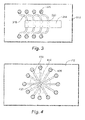
- the plurality of wire bond connections 320 can be spaced out along a length of the wire 314 and extend outward from opposite sides of the wire 314 thereby providing a plurality of wire bond connections 325 thereon.
- a plurality of relatively thin wires 318 comprise the wire bond and are coupled to wire 314 via bonding or mechanical clamping. The opposing ends of the thin wires 318 are bonded to the semiconductor chip 312 via friction welding.
- a plurality of thin wires 418 can connect to a common point 420 on a surface of wire 414 and radiate outwardly onto a surface of the semiconductor chip 412 thereby providing wire bond connections 425 in a circumferential pattern on the semiconductor chip 412.
Landscapes
- Wire Bonding (AREA)
Abstract
Description
- The present disclosure relates to integrated circuits, and more particularly to wire bonds for integrated circuits, MEMS devices, and the like.
- Wires in power electronics are used to conduct current to and from a device package. The package wires are attached to the electronic components inside the package by way of wire bonds. During operation power electronic modules are subject to temperature sway. Particularly at the wire bonds for semiconductor chips, significant temperature variation can be observed. Wire material, i.e., aluminum and copper, and semiconductor chips, i.e. silicon, have different thermal expansion coefficients. Under the elevated temperature, the wire bond is subject to shear load due to the thermal expansion mismatch. This can lead to wire bond failure. The intensity of thermal mismatch is directly related to three key factors: the temperature sway amplitude, the bond dimension, and the difference in the coefficients of thermal expansion (CTE). Each of these key factors can compromise the reliability of the wire bond. Most work focus on the reduction of the thermal temperature sway by meanings as improvement of the bonding technology to reduce the contact electrical resistance, or use large bond to reduce the current density.
- Various approaches have been developed to improve wire bond reliability. The mostly widely used concept is known as double stitch bonding. Instead of one stitch per wire, each wire is stitched multiple times onto a semiconductor chip. Another approach is using a flat ribbon wire instead of a round ribbon wire. The flat ribbon wire can achieve a relatively narrow bond with a bigger contact area. However, the bond dimension of either of these approaches is not reduced.
- Such conventional methods and systems have generally been considered satisfactory for their intended purpose. However, there is still a need in the art for improved wire bonds. The present disclosure provides a solution for this need by using a plurality of wire bonds with smaller dimensions.
- A circuit element includes a semiconductor chip and a wire for connecting between the semiconductor chip and an additional circuit element. A plurality of wire bond connections electrically connects the wire and the semiconductor chip. The plurality of wire bond connections can be disposed on a surface of the semiconductor chip and on a surface of the wire.
- A helical shaped wire can be used to electrically connect the semiconductor chip, wherein the plurality of wire bond connections includes a plurality of wire bond connections on the surface of the chip and a plurality of wire bond connections on the wire. The helical pitch length of the helical shaped wire can be greater than the wire diameter of the helical shaped wire bond for spacing the wire bond connections. The essence of the helical wire shape design is to reduce the bond dimension. As the result of the wire curvature from its helical shape, the wire bond can be made more symmetric in dimensions than the bond made from the conventional straight wire.
- The plurality of wire bond connections includes a plurality of individual wire bonds, each with a wire bond connection on the wire and a wire bond connection on the semiconductor chip. The plurality of individual wire bond connections can be spaced out along a length of the wire. The wire bond connections can extend outward from opposite side of the wire to the semiconductor chip. In certain embodiments, the wire bond connections can connect to a common point on the wire and radiate outward to wire bond connections on the semiconductor chip.
- These and other features of the systems and methods of the subject disclosure will become more readily apparent to those skilled in the art from the following detailed description of the preferred embodiments taken in conjunction with the drawings.
- So that those skilled in the art to which the subject disclosure appertains will readily understand how to make and use the devices and methods of the subject disclosure without undue experimentation, preferred embodiments thereof will be described by way of example and in detail herein below with reference to certain figures, wherein:
-
Fig. 1 is a perspective view of an exemplary integrated circuit, showing a plurality of wires electrically connecting a plurality of semiconductor chips; -
Fig. 2 is a perspective view of an exemplary embodiment of a wire bond constructed in accordance with the present disclosure showing a plurality of wire bond connections; -
Fig. 3 is a top plan view of another exemplary embodiment of a wire bond constructed in accordance with the present disclosure; and -
Fig. 4 is a top plan view of another exemplary embodiment of a wire bond constructed in accordance with the present disclosure. - Reference will now be made to the drawings wherein like reference numerals identify similar structural features or aspects of the subject disclosure. For purposes of explanation and illustration, and not limitation, a partial view of an exemplary embodiment of a wire bond design in accordance with the disclosure is shown in
Fig. 2 and is designated generally byreference character 100. Other embodiments of the wire bond design in accordance with the disclosure, or aspects thereof, are provided inFigs. 3-4 , as will be described. - The market for modern power electronics requires electrical components and connections therebetween to withstand high temperature ranges while maintaining high reliability. One of the barriers to meet these requirements is wire bond failure, which is one of the major failure modes of power electronic modules. Innovative wire bond design is the key factor to improve reliability. With reference to
Fig. 1 , a simplified embodiment of anintegrated circuit 10 as known in the prior art is shown as a perspective cutaway view. Thecircuit 10 includes at least onesemiconductor chip 12 electrically connected to a plurality ofpackage wires 14. Thewires 14 connect thesemiconductor chips 12 andpins 16.Pins 16 provide power to and from to thesemiconductor chips 12, e.g., by connectingpin 16 to a printed circuit board (PCB). Each of thewires 14 is bonded to therespective semiconductor chip 12. Typically in the prior art, the wire bonds are relatively large and asymmetric in dimension, e.g., for a 450 µm diameter wire, the wire bonds about 250 µm by 700 µm. The thermal mismatch is driven by the maximum dimension of the wire bonds, which is 700 mm using the above example. - To mitigate thermal mismatch, the present disclosure provides a solution to reducing bond dimension through wire bond designs without changing the overall bond area.
Fig. 2 illustrates an exemplary embodiment of the present disclosure showing acircuit element 100 having asemiconductor chip 112 and awire 122 providing electrical connection between thesemiconductor chip 112 and an additional circuit element, for example, a pin for connecting to a PCB. A portion of thewire 122 which connects tochip 112, is manufactured into a helical shape. A plurality ofwire bond connections 125 between thewire 122 and thesemiconductor chip 112 are provided along the helical-shaped portion of thewire 122. For example, instead of a 450 µm wire, the helical shapedwire 122 has a diameter of approximately 300 µm. Further, apitch 124 of the helicalshaped wire bond 122 is greater than a diameter d. In this manner, multiple separatedwire bond connections 125 are formed with dimensions about 150 µm by 150 µm. At least seven wire bond connections provide a total bond area similar to total bond area of conventional circuit element. Even though the total bond area is similar to conventional methods using a relatively thicker wire, the reduction of wire bond dimension from 700 µm to 150 µm mitigates the thermal mismatch between the semiconductor chip and the wire. Therefore, the life of the wire bond can be enhanced as well as the reliability of the circuit elements. - With reference to
Figs. 3 and 4 , additional exemplary embodiments of wire bond designs which provide a plurality of wire bond connections are shown. The plurality of wire bond connections include a plurality of individual wire bonds, each with a wire bond connection on the wire and a wire bond connection on the semiconductor chip. In the embodiment shown inFig. 3 , the plurality ofwire bond connections 320 can be spaced out along a length of thewire 314 and extend outward from opposite sides of thewire 314 thereby providing a plurality ofwire bond connections 325 thereon. A plurality of relativelythin wires 318 comprise the wire bond and are coupled to wire 314 via bonding or mechanical clamping. The opposing ends of thethin wires 318 are bonded to thesemiconductor chip 312 via friction welding. Similarly, in the embodiment shown inFig. 4 , a plurality ofthin wires 418 can connect to acommon point 420 on a surface ofwire 414 and radiate outwardly onto a surface of thesemiconductor chip 412 thereby providingwire bond connections 425 in a circumferential pattern on thesemiconductor chip 412. Those skilled in the art will readily appreciate that while described herein with specific examples, any other suitable wire bond arrangement and number of wire bond connections can be used without departing from the scope of this disclosure. - The methods and systems of the present disclosure, as described above and shown in the drawings, provide for a wire bond design with superior properties including improving the reliability and longevity of the wire bond, by reducing thermal mismatch through smaller wire bonds. While the apparatus and methods of the subject disclosure have been shown and described with reference to preferred embodiments, those skilled in the art will readily appreciate that changes and/or modifications may be made thereto without departing from the scope of the subject disclosure.
Claims (15)
- A circuit element (100), comprising:a semiconductor chip (112);a wire (122) for connecting between the semiconductor chip (112) and an additional circuit element; anda plurality of wire bond connections (125) electrically connecting the wire (122) and the semiconductor chip (112).
- The circuit element (100) of claim 1, wherein the plurality of wire bond connections (125) are disposed on a surface of the semiconductor chip (112).
- The circuit element (100) of claim 1, wherein the plurality of wire bond connections (125) are disposed on a surface of the wire (122).
- The circuit element (100) of claim 1, wherein a helical shaped wire electrically connects to the semiconductor chip (112) through the plurality of wire bond connections (125).
- The circuit element (100) of claim 4, wherein a pitch length of the helical shaped wire is greater than a wire diameter of the helical shaped wire bond.
- The circuit element (100) of claim 4, wherein the helical shaped wire bond is 150µm in thickness.
- The circuit element (100) of claim 1, wherein the plurality of wire bond connections (125) includes a plurality of individual wire bonds (320), each with a wire bond connection on the wire (122) and a wire bond connection on the semiconductor chip (112).
- The circuit element (100) of claim 7, wherein the plurality of individual wire bonds (320) are spaced out along a length of the wire and extend outwardly from opposite sides of the wire (122) to the semiconductor chip (112).
- The circuit element (100) of claim 7, wherein the plurality of individual wire bonds (320) can connect to a common point on the wire (122) and radiate outward to the wire bond connections on the semiconductor chip (112).
- The circuit element (100) of claim 1, wherein at least seven wire bond connections are disposed on a surface of the semiconductor chip (112).
- An integrated circuit (10) comprising:an integrated circuit package;a plurality of circuit elements disposed on a substrate within the integrated circuit package;a plurality of pins (16) electrically connecting to the plurality of circuit elements;a plurality of wires (14) connecting between the plurality of circuit elements and to the plurality of pins (16); anda plurality of wire bond connections (125) electrically connecting one wire with one circuit element.
- The integrated circuit of claim 11, wherein the plurality of wire bond connections (125) are disposed on a surface of the circuit element.
- The integrated circuit of claim 11, wherein the plurality of wire bond connections (125) are disposed on a surface of the wire.
- The integrated circuit of claim 11, wherein a helical shaped wire electrically connects the circuit element through the plurality of wire bond connections (125).
- The integrated circuit of claim 11, wherein a pitch of the helical shaped wire is greater than a thickness of the helical shaped wire bond.
Applications Claiming Priority (1)
| Application Number | Priority Date | Filing Date | Title |
|---|---|---|---|
| US14/459,011 US9275970B1 (en) | 2014-08-13 | 2014-08-13 | Wire bonds for electronics |
Publications (3)
| Publication Number | Publication Date |
|---|---|
| EP2985789A2 true EP2985789A2 (en) | 2016-02-17 |
| EP2985789A3 EP2985789A3 (en) | 2016-05-25 |
| EP2985789B1 EP2985789B1 (en) | 2019-06-05 |
Family
ID=53835337
Family Applications (1)
| Application Number | Title | Priority Date | Filing Date |
|---|---|---|---|
| EP15180682.5A Active EP2985789B1 (en) | 2014-08-13 | 2015-08-12 | Helical bond wire connection |
Country Status (2)
| Country | Link |
|---|---|
| US (1) | US9275970B1 (en) |
| EP (1) | EP2985789B1 (en) |
Families Citing this family (2)
| Publication number | Priority date | Publication date | Assignee | Title |
|---|---|---|---|---|
| US9717148B2 (en) * | 2015-09-18 | 2017-07-25 | Quartzdyne, Inc. | Methods of forming a microelectronic device structure, and related microelectronic device structures and microelectronic devices |
| US10600756B1 (en) | 2017-02-15 | 2020-03-24 | United States Of America, As Represented By The Secretary Of The Navy | Wire bonding technique for integrated circuit board connections |
Family Cites Families (10)
| Publication number | Priority date | Publication date | Assignee | Title |
|---|---|---|---|---|
| US4824005A (en) * | 1986-08-13 | 1989-04-25 | Orthodyne Electronics Corporation | Dual mode ultrasonic generator in a wire bonding apparatus |
| US6835898B2 (en) * | 1993-11-16 | 2004-12-28 | Formfactor, Inc. | Electrical contact structures formed by configuring a flexible wire to have a springable shape and overcoating the wire with at least one layer of a resilient conductive material, methods of mounting the contact structures to electronic components, and applications for employing the contact structures |
| US6285075B1 (en) * | 1998-11-02 | 2001-09-04 | Asat, Limited | Integrated circuit package with bonding planes on a ceramic ring using an adhesive assembly |
| US6313523B1 (en) * | 1999-10-28 | 2001-11-06 | Hewlett-Packard Company | IC die power connection using canted coil spring |
| US6522018B1 (en) * | 2000-05-16 | 2003-02-18 | Micron Technology, Inc. | Ball grid array chip packages having improved testing and stacking characteristics |
| JP3975181B2 (en) * | 2003-06-11 | 2007-09-12 | 三菱電機株式会社 | Power semiconductor device |
| US6958616B1 (en) * | 2003-11-07 | 2005-10-25 | Xilinx, Inc. | Hybrid interface apparatus for testing integrated circuits having both low-speed and high-speed input/output pins |
| US20070296056A1 (en) * | 2006-06-27 | 2007-12-27 | Texas Instruments Incorporated | Integrated Circuits Having Controlled Inductances |
| DE102009002191B4 (en) * | 2009-04-03 | 2012-07-12 | Infineon Technologies Ag | Power semiconductor module, power semiconductor module assembly, and method of making a power semiconductor module assembly |
| JP5678884B2 (en) * | 2009-08-03 | 2015-03-04 | 株式会社安川電機 | Power converter |
-
2014
- 2014-08-13 US US14/459,011 patent/US9275970B1/en active Active
-
2015
- 2015-08-12 EP EP15180682.5A patent/EP2985789B1/en active Active
Non-Patent Citations (1)
| Title |
|---|
| None |
Also Published As
| Publication number | Publication date |
|---|---|
| US9275970B1 (en) | 2016-03-01 |
| EP2985789B1 (en) | 2019-06-05 |
| US20160049380A1 (en) | 2016-02-18 |
| EP2985789A3 (en) | 2016-05-25 |
Similar Documents
| Publication | Publication Date | Title |
|---|---|---|
| US10943871B2 (en) | Semiconductor device having conductive wire with increased attachment angle and method | |
| US8971054B2 (en) | Component assembly | |
| CN105814687B (en) | Semiconductor package and its mounting structure | |
| US20090008796A1 (en) | Copper on organic solderability preservative (osp) interconnect | |
| US20110186999A1 (en) | Semiconductor device and method for manufacturing the same | |
| US20100116869A1 (en) | Electrical Microfilament to Circuit Interface | |
| JP6363825B2 (en) | Semiconductor device and lead frame | |
| US7476965B2 (en) | Electronic device with integrated heat distributor | |
| EP2985789B1 (en) | Helical bond wire connection | |
| EP3644358B1 (en) | Power semiconductor module arrangement including a contact element | |
| US9847279B2 (en) | Composite lead frame structure | |
| US20130069217A1 (en) | Semiconductor device and electrode terminal | |
| JP6959785B2 (en) | Circuit boards, electronic components and electronic modules | |
| KR20190108163A (en) | Electronic devices and accessors | |
| CN110168709B (en) | Semiconductor module with first and second connecting elements for connecting semiconductor chips and manufacturing method | |
| JP2017135148A (en) | Semiconductor device | |
| EP1235273A2 (en) | Semiconductor device formed by mounting semiconductor chip on support substrate, and the support substrate | |
| JP4954778B2 (en) | Three-dimensional electronic circuit device and connecting member | |
| TWI616992B (en) | Semiconductor device | |
| JP6254807B2 (en) | Semiconductor device and electronic equipment | |
| JP2006040995A (en) | Wiring board and semiconductor device | |
| JP6923687B2 (en) | Light emitting device | |
| JP4523425B2 (en) | Semiconductor device mounting substrate | |
| JP7025845B2 (en) | Wiring boards, electronic devices and electronic modules |
Legal Events
| Date | Code | Title | Description |
|---|---|---|---|
| PUAI | Public reference made under article 153(3) epc to a published international application that has entered the european phase |
Free format text: ORIGINAL CODE: 0009012 |
|
| AK | Designated contracting states |
Kind code of ref document: A2 Designated state(s): AL AT BE BG CH CY CZ DE DK EE ES FI FR GB GR HR HU IE IS IT LI LT LU LV MC MK MT NL NO PL PT RO RS SE SI SK SM TR |
|
| AX | Request for extension of the european patent |
Extension state: BA ME |
|
| PUAL | Search report despatched |
Free format text: ORIGINAL CODE: 0009013 |
|
| AK | Designated contracting states |
Kind code of ref document: A3 Designated state(s): AL AT BE BG CH CY CZ DE DK EE ES FI FR GB GR HR HU IE IS IT LI LT LU LV MC MK MT NL NO PL PT RO RS SE SI SK SM TR |
|
| AX | Request for extension of the european patent |
Extension state: BA ME |
|
| RIC1 | Information provided on ipc code assigned before grant |
Ipc: H01L 23/49 20060101AFI20160420BHEP |
|
| STAA | Information on the status of an ep patent application or granted ep patent |
Free format text: STATUS: REQUEST FOR EXAMINATION WAS MADE |
|
| 17P | Request for examination filed |
Effective date: 20161118 |
|
| RBV | Designated contracting states (corrected) |
Designated state(s): AL AT BE BG CH CY CZ DE DK EE ES FI FR GB GR HR HU IE IS IT LI LT LU LV MC MK MT NL NO PL PT RO RS SE SI SK SM TR |
|
| STAA | Information on the status of an ep patent application or granted ep patent |
Free format text: STATUS: EXAMINATION IS IN PROGRESS |
|
| 17Q | First examination report despatched |
Effective date: 20170421 |
|
| GRAP | Despatch of communication of intention to grant a patent |
Free format text: ORIGINAL CODE: EPIDOSNIGR1 |
|
| STAA | Information on the status of an ep patent application or granted ep patent |
Free format text: STATUS: GRANT OF PATENT IS INTENDED |
|
| INTG | Intention to grant announced |
Effective date: 20181218 |
|
| GRAS | Grant fee paid |
Free format text: ORIGINAL CODE: EPIDOSNIGR3 |
|
| GRAA | (expected) grant |
Free format text: ORIGINAL CODE: 0009210 |
|
| STAA | Information on the status of an ep patent application or granted ep patent |
Free format text: STATUS: THE PATENT HAS BEEN GRANTED |
|
| AK | Designated contracting states |
Kind code of ref document: B1 Designated state(s): AL AT BE BG CH CY CZ DE DK EE ES FI FR GB GR HR HU IE IS IT LI LT LU LV MC MK MT NL NO PL PT RO RS SE SI SK SM TR |
|
| REG | Reference to a national code |
Ref country code: GB Ref legal event code: FG4D |
|
| REG | Reference to a national code |
Ref country code: CH Ref legal event code: EP |
|
| REG | Reference to a national code |
Ref country code: AT Ref legal event code: REF Ref document number: 1140852 Country of ref document: AT Kind code of ref document: T Effective date: 20190615 |
|
| REG | Reference to a national code |
Ref country code: IE Ref legal event code: FG4D |
|
| REG | Reference to a national code |
Ref country code: DE Ref legal event code: R096 Ref document number: 602015031285 Country of ref document: DE |
|
| REG | Reference to a national code |
Ref country code: NL Ref legal event code: MP Effective date: 20190605 |
|
| REG | Reference to a national code |
Ref country code: LT Ref legal event code: MG4D |
|
| PG25 | Lapsed in a contracting state [announced via postgrant information from national office to epo] |
Ref country code: HR Free format text: LAPSE BECAUSE OF FAILURE TO SUBMIT A TRANSLATION OF THE DESCRIPTION OR TO PAY THE FEE WITHIN THE PRESCRIBED TIME-LIMIT Effective date: 20190605 Ref country code: ES Free format text: LAPSE BECAUSE OF FAILURE TO SUBMIT A TRANSLATION OF THE DESCRIPTION OR TO PAY THE FEE WITHIN THE PRESCRIBED TIME-LIMIT Effective date: 20190605 Ref country code: LT Free format text: LAPSE BECAUSE OF FAILURE TO SUBMIT A TRANSLATION OF THE DESCRIPTION OR TO PAY THE FEE WITHIN THE PRESCRIBED TIME-LIMIT Effective date: 20190605 Ref country code: FI Free format text: LAPSE BECAUSE OF FAILURE TO SUBMIT A TRANSLATION OF THE DESCRIPTION OR TO PAY THE FEE WITHIN THE PRESCRIBED TIME-LIMIT Effective date: 20190605 Ref country code: NO Free format text: LAPSE BECAUSE OF FAILURE TO SUBMIT A TRANSLATION OF THE DESCRIPTION OR TO PAY THE FEE WITHIN THE PRESCRIBED TIME-LIMIT Effective date: 20190905 Ref country code: AL Free format text: LAPSE BECAUSE OF FAILURE TO SUBMIT A TRANSLATION OF THE DESCRIPTION OR TO PAY THE FEE WITHIN THE PRESCRIBED TIME-LIMIT Effective date: 20190605 Ref country code: SE Free format text: LAPSE BECAUSE OF FAILURE TO SUBMIT A TRANSLATION OF THE DESCRIPTION OR TO PAY THE FEE WITHIN THE PRESCRIBED TIME-LIMIT Effective date: 20190605 |
|
| PG25 | Lapsed in a contracting state [announced via postgrant information from national office to epo] |
Ref country code: GR Free format text: LAPSE BECAUSE OF FAILURE TO SUBMIT A TRANSLATION OF THE DESCRIPTION OR TO PAY THE FEE WITHIN THE PRESCRIBED TIME-LIMIT Effective date: 20190906 Ref country code: LV Free format text: LAPSE BECAUSE OF FAILURE TO SUBMIT A TRANSLATION OF THE DESCRIPTION OR TO PAY THE FEE WITHIN THE PRESCRIBED TIME-LIMIT Effective date: 20190605 Ref country code: RS Free format text: LAPSE BECAUSE OF FAILURE TO SUBMIT A TRANSLATION OF THE DESCRIPTION OR TO PAY THE FEE WITHIN THE PRESCRIBED TIME-LIMIT Effective date: 20190605 Ref country code: BG Free format text: LAPSE BECAUSE OF FAILURE TO SUBMIT A TRANSLATION OF THE DESCRIPTION OR TO PAY THE FEE WITHIN THE PRESCRIBED TIME-LIMIT Effective date: 20190905 |
|
| REG | Reference to a national code |
Ref country code: AT Ref legal event code: MK05 Ref document number: 1140852 Country of ref document: AT Kind code of ref document: T Effective date: 20190605 |
|
| PG25 | Lapsed in a contracting state [announced via postgrant information from national office to epo] |
Ref country code: AT Free format text: LAPSE BECAUSE OF FAILURE TO SUBMIT A TRANSLATION OF THE DESCRIPTION OR TO PAY THE FEE WITHIN THE PRESCRIBED TIME-LIMIT Effective date: 20190605 Ref country code: EE Free format text: LAPSE BECAUSE OF FAILURE TO SUBMIT A TRANSLATION OF THE DESCRIPTION OR TO PAY THE FEE WITHIN THE PRESCRIBED TIME-LIMIT Effective date: 20190605 Ref country code: NL Free format text: LAPSE BECAUSE OF FAILURE TO SUBMIT A TRANSLATION OF THE DESCRIPTION OR TO PAY THE FEE WITHIN THE PRESCRIBED TIME-LIMIT Effective date: 20190605 Ref country code: PT Free format text: LAPSE BECAUSE OF FAILURE TO SUBMIT A TRANSLATION OF THE DESCRIPTION OR TO PAY THE FEE WITHIN THE PRESCRIBED TIME-LIMIT Effective date: 20191007 Ref country code: CZ Free format text: LAPSE BECAUSE OF FAILURE TO SUBMIT A TRANSLATION OF THE DESCRIPTION OR TO PAY THE FEE WITHIN THE PRESCRIBED TIME-LIMIT Effective date: 20190605 Ref country code: RO Free format text: LAPSE BECAUSE OF FAILURE TO SUBMIT A TRANSLATION OF THE DESCRIPTION OR TO PAY THE FEE WITHIN THE PRESCRIBED TIME-LIMIT Effective date: 20190605 Ref country code: SK Free format text: LAPSE BECAUSE OF FAILURE TO SUBMIT A TRANSLATION OF THE DESCRIPTION OR TO PAY THE FEE WITHIN THE PRESCRIBED TIME-LIMIT Effective date: 20190605 |
|
| PG25 | Lapsed in a contracting state [announced via postgrant information from national office to epo] |
Ref country code: SM Free format text: LAPSE BECAUSE OF FAILURE TO SUBMIT A TRANSLATION OF THE DESCRIPTION OR TO PAY THE FEE WITHIN THE PRESCRIBED TIME-LIMIT Effective date: 20190605 Ref country code: IS Free format text: LAPSE BECAUSE OF FAILURE TO SUBMIT A TRANSLATION OF THE DESCRIPTION OR TO PAY THE FEE WITHIN THE PRESCRIBED TIME-LIMIT Effective date: 20191005 Ref country code: IT Free format text: LAPSE BECAUSE OF FAILURE TO SUBMIT A TRANSLATION OF THE DESCRIPTION OR TO PAY THE FEE WITHIN THE PRESCRIBED TIME-LIMIT Effective date: 20190605 |
|
| REG | Reference to a national code |
Ref country code: DE Ref legal event code: R097 Ref document number: 602015031285 Country of ref document: DE |
|
| PG25 | Lapsed in a contracting state [announced via postgrant information from national office to epo] |
Ref country code: TR Free format text: LAPSE BECAUSE OF FAILURE TO SUBMIT A TRANSLATION OF THE DESCRIPTION OR TO PAY THE FEE WITHIN THE PRESCRIBED TIME-LIMIT Effective date: 20190605 |
|
| PLBE | No opposition filed within time limit |
Free format text: ORIGINAL CODE: 0009261 |
|
| STAA | Information on the status of an ep patent application or granted ep patent |
Free format text: STATUS: NO OPPOSITION FILED WITHIN TIME LIMIT |
|
| PG25 | Lapsed in a contracting state [announced via postgrant information from national office to epo] |
Ref country code: DK Free format text: LAPSE BECAUSE OF FAILURE TO SUBMIT A TRANSLATION OF THE DESCRIPTION OR TO PAY THE FEE WITHIN THE PRESCRIBED TIME-LIMIT Effective date: 20190605 Ref country code: PL Free format text: LAPSE BECAUSE OF FAILURE TO SUBMIT A TRANSLATION OF THE DESCRIPTION OR TO PAY THE FEE WITHIN THE PRESCRIBED TIME-LIMIT Effective date: 20190605 |
|
| 26N | No opposition filed |
Effective date: 20200306 |
|
| PG25 | Lapsed in a contracting state [announced via postgrant information from national office to epo] |
Ref country code: MC Free format text: LAPSE BECAUSE OF FAILURE TO SUBMIT A TRANSLATION OF THE DESCRIPTION OR TO PAY THE FEE WITHIN THE PRESCRIBED TIME-LIMIT Effective date: 20190605 Ref country code: LU Free format text: LAPSE BECAUSE OF NON-PAYMENT OF DUE FEES Effective date: 20190812 Ref country code: SI Free format text: LAPSE BECAUSE OF FAILURE TO SUBMIT A TRANSLATION OF THE DESCRIPTION OR TO PAY THE FEE WITHIN THE PRESCRIBED TIME-LIMIT Effective date: 20190605 Ref country code: LI Free format text: LAPSE BECAUSE OF NON-PAYMENT OF DUE FEES Effective date: 20190831 Ref country code: CH Free format text: LAPSE BECAUSE OF NON-PAYMENT OF DUE FEES Effective date: 20190831 |
|
| REG | Reference to a national code |
Ref country code: BE Ref legal event code: MM Effective date: 20190831 |
|
| PG25 | Lapsed in a contracting state [announced via postgrant information from national office to epo] |
Ref country code: IE Free format text: LAPSE BECAUSE OF NON-PAYMENT OF DUE FEES Effective date: 20190812 |
|
| PG25 | Lapsed in a contracting state [announced via postgrant information from national office to epo] |
Ref country code: BE Free format text: LAPSE BECAUSE OF NON-PAYMENT OF DUE FEES Effective date: 20190831 |
|
| PG25 | Lapsed in a contracting state [announced via postgrant information from national office to epo] |
Ref country code: CY Free format text: LAPSE BECAUSE OF FAILURE TO SUBMIT A TRANSLATION OF THE DESCRIPTION OR TO PAY THE FEE WITHIN THE PRESCRIBED TIME-LIMIT Effective date: 20190605 |
|
| PG25 | Lapsed in a contracting state [announced via postgrant information from national office to epo] |
Ref country code: MT Free format text: LAPSE BECAUSE OF FAILURE TO SUBMIT A TRANSLATION OF THE DESCRIPTION OR TO PAY THE FEE WITHIN THE PRESCRIBED TIME-LIMIT Effective date: 20190605 Ref country code: HU Free format text: LAPSE BECAUSE OF FAILURE TO SUBMIT A TRANSLATION OF THE DESCRIPTION OR TO PAY THE FEE WITHIN THE PRESCRIBED TIME-LIMIT; INVALID AB INITIO Effective date: 20150812 |
|
| PG25 | Lapsed in a contracting state [announced via postgrant information from national office to epo] |
Ref country code: MK Free format text: LAPSE BECAUSE OF FAILURE TO SUBMIT A TRANSLATION OF THE DESCRIPTION OR TO PAY THE FEE WITHIN THE PRESCRIBED TIME-LIMIT Effective date: 20190605 |
|
| P01 | Opt-out of the competence of the unified patent court (upc) registered |
Effective date: 20230522 |
|
| PGFP | Annual fee paid to national office [announced via postgrant information from national office to epo] |
Ref country code: DE Payment date: 20250724 Year of fee payment: 11 |
|
| PGFP | Annual fee paid to national office [announced via postgrant information from national office to epo] |
Ref country code: GB Payment date: 20250724 Year of fee payment: 11 |
|
| PGFP | Annual fee paid to national office [announced via postgrant information from national office to epo] |
Ref country code: FR Payment date: 20250725 Year of fee payment: 11 |
|
| REG | Reference to a national code |
Ref country code: DE Ref legal event code: R079 Ref document number: 602015031285 Country of ref document: DE Free format text: PREVIOUS MAIN CLASS: H01L0023490000 Ipc: H10W0072500000 |