EP2985737A1 - Graphics processing circuit having second vertex shader configured to reuse output of first vertex shader and/or process repacked vertex thread group and related graphics processing method thereof - Google Patents

Graphics processing circuit having second vertex shader configured to reuse output of first vertex shader and/or process repacked vertex thread group and related graphics processing method thereof Download PDF

Info

Publication number
EP2985737A1
EP2985737A1 EP14181247.9A EP14181247A EP2985737A1 EP 2985737 A1 EP2985737 A1 EP 2985737A1 EP 14181247 A EP14181247 A EP 14181247A EP 2985737 A1 EP2985737 A1 EP 2985737A1
Authority
EP
European Patent Office
Prior art keywords
vertex
graphics processing
value
values
vertices
Prior art date
Legal status (The legal status is an assumption and is not a legal conclusion. Google has not performed a legal analysis and makes no representation as to the accuracy of the status listed.)
Ceased
Application number
EP14181247.9A
Other languages
German (de)
French (fr)
Inventor
Jia-Yang Chang
Current Assignee (The listed assignees may be inaccurate. Google has not performed a legal analysis and makes no representation or warranty as to the accuracy of the list.)
MediaTek Inc
Original Assignee
MediaTek Inc
Priority date (The priority date is an assumption and is not a legal conclusion. Google has not performed a legal analysis and makes no representation as to the accuracy of the date listed.)
Filing date
Publication date
Application filed by MediaTek Inc filed Critical MediaTek Inc
Publication of EP2985737A1 publication Critical patent/EP2985737A1/en
Ceased legal-status Critical Current

Links

Images

Classifications

    • GPHYSICS
    • G06COMPUTING OR CALCULATING; COUNTING
    • G06TIMAGE DATA PROCESSING OR GENERATION, IN GENERAL
    • G06T15/00Three-dimensional [3D] image rendering
    • G06T15/50Lighting effects
    • G06T15/80Shading
    • GPHYSICS
    • G06COMPUTING OR CALCULATING; COUNTING
    • G06TIMAGE DATA PROCESSING OR GENERATION, IN GENERAL
    • G06T15/00Three-dimensional [3D] image rendering
    • G06T15/005General purpose rendering architectures
    • GPHYSICS
    • G06COMPUTING OR CALCULATING; COUNTING
    • G06TIMAGE DATA PROCESSING OR GENERATION, IN GENERAL
    • G06T1/00General purpose image data processing
    • G06T1/20Processor architectures; Processor configuration, e.g. pipelining
    • GPHYSICS
    • G06COMPUTING OR CALCULATING; COUNTING
    • G06TIMAGE DATA PROCESSING OR GENERATION, IN GENERAL
    • G06T1/00General purpose image data processing
    • G06T1/60Memory management

Definitions

  • the disclosed embodiments of the present invention relate to a graphics processing circuit having a second vertex shader configured to reuse an output of a first vertex shader and/or process a repacked vertex thread group and related graphics processing method thereof.
  • a graphics processing unit may only use fixed computational units to process the graphics data. More recently, a portion of the graphics processing unit may be implemented using programmable computational units to support a wider variety of operations. For example, a vertex shader may be made programmable.
  • the vertex shading operation may be split into a first vertex shading stage and a second vertex shading stage.
  • the vertex shading operation includes multiple instructions. Though the vertex shading operation may be divided into two vertex shading stages, the instructions cannot be divided into two mutually exclusive instruction sets for the vertex shading stages.
  • instructions of the vertex shading operation contain first instructions, second instructions and third instructions.
  • One instruction set executed by the first vertex shading stage may include the first instructions and the second instructions, while the other instruction set executed by the second vertex shading stage may include the first instructions and the third instructions.
  • the conventional design of dividing the vertex shading operation into two vertex shading stages may allow the first vertex shading stage to skip the execution of the third instructions; however, the first instructions executed by the first vertex shading stage are needed to be executed by the second vertex shading stage again. As a result, the conventional design of dividing the vertex shading operation into two vertex shading stages is not efficient in instruction execution.
  • the present invention aims at providing a graphics processing circuit having a second vertex shader configured to reuse an output of a first vertex shader and/or process a repacked vertex thread group and related graphics processing method thereof, to improve the instruction execution efficiency of a vertex shader design using multiple vertex shading stages.
  • the claimed graphics processing circuit includes a buffer, a first vertex shader, and a second vertex shader.
  • the first vertex shader is configured to generate at least coordinate values of a plurality of vertices to the buffer.
  • the second vertex shader is configured to read at least a portion of buffered coordinate values from the buffer, and reuse at least the portion of the buffered coordinate values to generate a value of at least one user-defined variable.
  • the claimed graphics processing method includes: performing a first vertex shading operation to generate at least coordinate values of a plurality of vertices to a buffer; and performing a second vertex shading operation to read at least a portion of buffered coordinate values from the buffer, and reuse at least the portion of the buffered coordinate values to generate a value of at least one user-defined variable.
  • One technical feature of the present invention is to reuse coordinate values generated from a first vertex shading stage to generate variable values (e.g., user-defined variable values such as varying variable values), thus reducing the number of instructions/calculations performed in a second vertex shading stage.
  • Another technical feature of the present invention is to reuse intermediate values generated from the first vertex shading stage to generate variable values (e.g., user-defined variable values such as varying variable values), thus reducing the number of instructions/calculations performed in the second vertex shading stage.
  • Yet another technical feature of the present invention is to repack non-rejected vertices in original vertex thread groups having one or more rejected vertices to generate a new vertex thread group filled with non-rejected vertices only, thus improving the performance of the second vertex shading stage. Further details of the proposed vertex shading design are described as below.
  • FIG. 1 is a diagram illustrating a graphics processing circuit according to a first embodiment of the present invention.
  • the graphics processing circuit 100 may be part of a graphics processing unit (GPU) used in an electronic device.
  • the graphics processing circuit 100 includes a first vertex shader 102, a vertex output buffer 104, a second vertex shader 106, and a primitive culling circuit 108. It should be noted that only the components pertinent to the present invention are shown in FIG. 1 . In practice, the graphics processing circuit 100 may have additional circuit blocks, depending upon actual design consideration.
  • the vertex output buffer 104 is coupled to the first vertex shader 102, the primitive culling circuit 108, and the second vertex shader 106. Hence, the vertex output buffer 104 is accessible to each of the first vertex shader 102, the primitive culling circuit 108, and the second vertex shader 106.
  • the first vertex shader 102 is configured to generate coordinate values of a plurality of vertices within the image geometry, and store the coordinate values of the vertices into the vertex output buffer 104. That is, the data output VS_OUT1 generated from the first vertex shader 102 to the vertex output buffer 104 includes vertex coordinate values.
  • the primitive culling circuit 108 is configured to find primitives associated with vertices in the vertex output buffer 104, and performs a culling process to reject certain primitives.
  • the primitive culling circuit 108 refers to the coordinate values of the vertices in the vertex output buffer 104 to distinguish between visible primitives and non-visible primitives, and generates one notification signal S1 to instruct a primitive buffer (not shown) to remove rejected primitives (e.g., non-visible primitives).
  • the primitive culling circuit 108 further generates another notification signal S2 to instruct the vertex output buffer 104 to reject vertices associated with the rejected primitives (e.g., non-visible primitives) by removing buffered coordinate values of the rejected vertices. Since the non-visible primitives will not be displayed on a display screen, removing the non-visible primitives can reduce the work load of the following primitive processing circuit. Similarly, removing vertices associated with non-visible primitives can reduce the work load of the following vertex processing circuit (e.g., the second vertex shader 106). That is, the second vertex shader 106 does not waste time on processing vertices associated with the rejected vertices.
  • the following vertex processing circuit e.g., the second vertex shader 106
  • the second vertex shader 106 is configured to read at least a portion (i.e., part or all) of buffered coordinate values from the vertex output buffer 104, and reuse at least the portion of the buffered coordinate values to generate a value of at least one user-defined variable.
  • the at least one user-defined variable may include at least one varying variable as defined by OpenGL ES (OpenGL for Embedded Systems). Since the coordinate values generated from the first vertex shader 102 are buffered and reused, the number of instructions/calculations executed by the second vertex shader 106 can be reduced greatly.
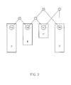
  • FIG. 2 is a simplified expression tree diagram illustrating an original vertex shading operation.
  • FIG. 3 is a simplified expression tree diagram illustrating a first vertex shading operation performed by the first vertex shader 102 in FIG. 1 and a second vertex shading operation performed by the second vertex shader 106 in FIG. 1 according to an embodiment of the present invention.
  • the expression of the original vertex shading operation may include sub-trees A, B, C, D, where each of the sub-trees A, B, C, D may include a plurality of sub-expressions, each corresponding to one instruction.
  • the sub-tree A generates an output value VA
  • the sub-tree B generates an output value VB
  • the sub-tree C generates an output value VC
  • the sub-tree D generates an output value VD.
  • the original vertex shading operation is executed to produce four final output values (VA+VB), (VB-VC), (VB-VC)xVD, and (VC/VD), where (VA+VB) is an output of the operand "+”, (VB-VC) is an output of the operand "-”, (VB-VC)xVD is an output of the operand "X”, and (VC/VD) is an output of the operand "/".
  • the original vertex shading operation is separated into a first vertex shading operation and a second vertex shading operation with a reduced number of overlapped instructions (i.e., the same instructions executed in both of the first vertex shading operation and the second vertex shading operation).
  • the first vertex shader 102 is responsible for generating two final output values (VA+VB) and (VB-VC) which may be vertex coordinate values; and the second vertex shader 104 is responsible for generating two final output values (VB-VC)xVD and (VC/VD) which may be varying variable values.
  • the first vertex shader 102 needs to execute at least instructions in sub-trees A, B, C and instructions corresponding to the operands "+” and "-”, and then generates the final output values (VA+VB) and (VB-VC) to the vertex output buffer 104. Since the final output value (VB-VC) is already available in the vertex output buffer 104, the second vertex shader 106 may directly load the final output value (VB-VC) from the vertex output buffer 104, and reuse the output value (VB-VC) to thereby skip the execution of instructions included in the sub-tree B.
  • the second vertex shader 106 executes instructions in sub-trees C, D and instructions corresponding to the operands "*" and “/”, and then generates the final output values (VB-VC)xVD and (VC/VD).
  • the proposed graphics processing circuit 100 allows the second vertex shader 106 to execute a reduced number of instructions due to the reuse of first vertex shader's output (e.g., vertex coordinate value(s) generated from the first vertex shader 102).
  • An example of reusing the first vertex shader's output, including at least one vertex coordinate value, may be illustrated by following program codes.
  • the first vertex shader 102 calculates the vertex coordinate value "gl_position", and the second vertex shader 106 needs to calculate the varying variable "v_position” only.
  • the second vertex shader 106 can get "position.z” from the vertex coordinate value "gl_position” generated by the first vertex shader 102.
  • the instruction count can be changed from 75 to 10, thus leading to enhanced performance of the second vertex shader 106.
  • the highest node in the sub-tree C is a boundary node whose value is involved in a direct calculation of first vertex shader's output (e.g., (VB-VC)) and a direct calculation of second vertex shader's output (e.g., (VC/VD)).
  • the output value VC of the sub-tree C may be regarded as an intermediate value of the vertex shading processing. If the output value VC is also stored into the vertex output buffer 104, the second vertex shader 106 may directly load the output value VC from the vertex output buffer 104 and reuse the output value VC to skip more instructions, thus leading to better performance of the second vertex shader 106.
  • FIG. 4 is a diagram illustrating a graphics processing circuit according to a second embodiment of the present invention.
  • the graphics processing circuit 400 may be part of a graphics processing unit (GPU) used in an electronic device.
  • the graphics processing circuit 400 includes a first vertex shader 402, a second vertex shader 406, and the aforementioned vertex output buffer 104 and primitive culling circuit 108. It should be noted that only the components pertinent to the present invention are shown in FIG. 4 . In practice, the graphics processing circuit 400 may have additional circuit blocks, depending upon actual design consideration.
  • the vertex output buffer 104 is coupled to the first vertex shader 402, the primitive culling circuit 108, and the second vertex shader 406. Hence, the vertex output buffer 104 is accessible to each of the first vertex shader 402, the primitive culling circuit 108, and the second vertex shader 406.
  • the first vertex shader 402 is configured to generate coordinate values of a plurality of vertices within image geometry, and store the coordinate values of the vertices into the vertex output buffer 104.
  • the first vertex shader 402 is further configured to generate a plurality of intermediate values, each associated with generation of a coordinate value of one of the vertices and generation of a value of at least one user-defined variable (e.g., a varying variable as defined by OpenGL ES), to the vertex output buffer 104. That is, the data output VS_OUT1' generated from the first vertex shader 402 to the vertex output buffer 104 includes vertex coordinate values and intermediate values.
  • the primitive culling circuit 108 instructs the vertex output buffer 104 to reject vertices associated with rejected primitives (e.g., non-visible primitives) by removing buffered coordinate values of the rejected vertices.
  • the second vertex shader 406 does not waste time on processing vertices associated with the rejected vertices.
  • the second vertex shader 406 is configured to read at least a portion (i.e., part or all) of buffered coordinate values and at least a portion (i.e., part or all) of buffered intermediate values from the vertex output buffer 104, and generate the value of the at least one user-defined variable by reusing at least the portion of the buffered coordinate values and at least the portion of the buffered intermediate values.
  • intermediate values may be reused by the second vertex shader 406. Since intermediate values are reused, more instructions can be skipped in the second vertex shader 406.
  • FIG. 5 is a simplified expression tree diagram illustrating a first vertex shading operation performed by the first vertex shader 402 in FIG. 4 and a second vertex shading operation performed by the second vertex shader 406 in FIG. 4 according to an embodiment of the present invention.
  • the major difference between the second vertex shading operations shown in FIG. 3 and FIG. 5 is that sub-tree C's output value VC needed by the second vertex shader 406 is directly loaded from the vertex output buffer 104, rather than derived from executing instructions included in the sub-tree C.
  • the first vertex shader 402 is responsible for generating final output values (VA+VB) and (VB-VC) which may be vertex coordinate values, and storing the final output values (VA+VB) and (VB-VC) and the output value VC (which is an intermediate value) to the vertex output buffer 104; and the second vertex shader 104 is responsible for loading the final output values (VB-VC) and the intermediate value VC from the vertex output buffer 104, and generating final output values (VB-VC)xVD and (VC/VD) which may be varying variable values.
  • the first vertex shader 402 needs to execute instructions in sub-trees A, B, C and instructions corresponding to the operands "+" and "-". Since the final output values (VB-VC) and the intermediate value VC are already available in the vertex output buffer 104, the second vertex shader 406 may directly load the final output values (VB-VC) and the intermediate value VC from the vertex output buffer 104, and reuse the final output values (VB-VC) and the intermediate VC to thereby skip the execution of instructions included in the sub-trees B and C.
  • the second vertex shader 406 executes instructions in sub-tree D and instructions corresponding to the operands "X" and "/" to generate the final output values (VB-VC)xVD and (VC/VD).
  • the proposed graphics processing circuit 400 shown in FIG. 4 allows the second vertex shader 406 to execute a reduced number of instructions due to the reuse of first vertex shader's output, including at least one vertex coordinate value and at least one intermediate value.
  • An example of reusing the first vertex shader's output, including at least one intermediate value, may be illustrated by following program codes.
  • the first vertex shader 102 calculates the vertex coordinate value "gl_position” based on the intermediate value "position", and the second vertex shader 106 needs to calculate the varying variable "fog_distance” based on the varying variable "fog_position", where the varying variable "fog_position” is obtained based on the intermediate value "position”.
  • the second vertex shader 406 can get "position” from the first vertex shader 402. With the reuse of first vertex shader's output, the instruction count can be changed from 126 to 24, thus leading to enhanced performance of the second vertex shader 406.
  • the first vertex shader's output including at least one vertex coordinate value and at least one intermediate value, is reused by the second vertex shader 406.
  • reusing both of the vertex coordinate value and the intermediate value is for illustrative purposes only, and is not meant to be a limitation of the present invention.
  • Any graphics processing design having a second vertex shader configured to reuse at least one intermediate value generated from a first vertex shader to generate a value of at least one variable still falls within the scope of the present invention.
  • the same objective of reducing the number of instructions executed in the second vertex shading stage is also achieved by reusing intermediate values.
  • the first vertex shader 402 is further configured to determine a plurality of weighting values for the candidate intermediate values, each associated with generation of at least one vertex coordinate value and generation of at least one variable value (e.g., a user-defined variable such as a varying variable), where a weighting value of a candidate intermediate value is proportional to the number of instructions needed to be executed for obtaining the candidate intermediate value.
  • a weighting value of a candidate intermediate value is proportional to the number of instructions needed to be executed for obtaining the candidate intermediate value.
  • node N5 is a boundary node whose value is directly used by the first vertex shader 402 to calculate a vertex coordinate value and/or directly used by the second vertex shader 402 to calculate a user-defined variable value.
  • the sub-tree 1 includes K1 instructions/calculations involved in calculating an output value at node N1.
  • the sub-tree 2 includes K2 instructions/calculations involved in calculating an output value at node N2.
  • An output value at node N3 is obtained by performing one instruction based on the output values at nodes N1 and N2.
  • An output value at node N4 is obtained by performing one instruction.
  • An output value at node N5 (i.e., one candidate intermediate value) is obtained by performing one instruction based on the output values at nodes N3 and N4. Therefore, the weighting value for the candidate intermediate value may be set by K1+K2+3.
  • the first vertex shader 402 compares the weighting values to select a portion of the candidate intermediate values as the selected intermediate values to be stored into the vertex output buffer 104. For example, the first vertex shader 402 sorts the weighting values of the candidate intermediate values, and then selects some candidate intermediate values, each having a weighting value larger than that possessed by remaining candidate intermediate values, as the selected intermediate values.
  • candidate intermediate values are not necessarily the values of boundary nodes.
  • the first vertex shader 402 is configured to determine a plurality of numbers of saved instructions (i.e., saved instruction counts) for a plurality of candidate intermediate values, each associated with generation of at least one vertex coordinate value and generation of at least one variable value (e.g., a user-defined variable such as a varying variable value).
  • FIG. 7 is a diagram illustrating an example of calculating the number of saved instructions (i.e., a saved instruction count) for a candidate intermediate value.
  • the values at nodes N1, N2, and N3 are associated with generation of one vertex coordinate value in the first vertex shader 402 and generation of one variable value in the second vertex shader 406.
  • the nodes N1 and N2 may be boundary nodes.
  • the values at nodes N1, N2, and N3, however, are all regarded as candidate intermediate values. If the candidate intermediate value at node N1 is treated as a selected intermediate value, only two instructions are saved in the second vertex shader 406 since the value at node N3 is needed to calculate the value at node N2, and instructions used for calculating the value at node N3 will still be executed by the second vertex shader 406.
  • the candidate intermediate value at node N2 is treated as a selected intermediate value, only two instructions are saved in the second vertex shader 406 since the value at node N3 is needed to calculate the value at node N1, and instructions used for calculating the value at node N3 will still be executed by the second vertex shader 406. If the candidate intermediate value at node N3 is treated as a selected intermediate value, four instructions are saved in the second vertex shader 406 since node N3 is a dominant node for nodes N4, N5 and N6 located underneath. Compared to candidate intermediate values at nodes N1 and N2, the candidate intermediate value at node N3 can save more instructions when reused by the second vertex shader 406. Hence, the candidate intermediate value at node N3 is selected and stored into the vertex output buffer 104 due to a larger saved instruction count.
  • the first vertex shader 402 compares the saved instruction counts to select a portion of the candidate intermediate values as the selected intermediate values to be stored in to the vertex output buffer. For example, the first vertex shader 402 sorts the saved instruction counts of the candidate intermediate values, and then selects some candidate intermediate values, each having a saved instruction count larger than that possessed by remaining candidate intermediate values, as the selected intermediate values.
  • each vertex shader may be implemented using a SIMD (single-instruction multiple-data) programmable shader for achieving better performance.
  • the present invention further proposes improving utilization of SIMD lanes through a compact vertex thread group.
  • FIG. 8 is a diagram illustrating a graphics processing circuit according to a third embodiment of the present invention.
  • the graphics processing circuit 800 may be part of a graphics processing unit (GPU) used in an electronic device.
  • the graphics processing circuit 800 includes a vertex repacking circuit 805 and the aforementioned first vertex shader 102 (or 402), second vertex shader 106 (or 406), vertex output buffer 104 and primitive culling circuit 108. It should be noted that only the components pertinent to the present invention are shown in FIG. 8 . In practice, the graphics processing circuit 800 may have additional circuit blocks, depending upon actual design consideration.
  • a vertex shader may employ processing techniques such as pipelining that attempts to process in parallel as much graphics data as possible.
  • a vertex shader with SIMD architecture is designed to maximize the amount of parallel processing in the graphics pipeline.
  • the same instruction is executed in parallel to process multiple data inputs. That is, threads of one thread group are synchronously executed through a plurality of SIMD lanes.
  • the second vertex shader 106/406 may be a SIMD programmable shader with a fixed number of SIMD lanes (i.e., execution units).
  • the primitive culling circuit 108 instructs the vertex output buffer 104 to reject vertices associated with rejected primitives (e.g., non-visible primitives) by removing buffered coordinate values of the rejected vertices.
  • rejected primitives e.g., non-visible primitives
  • the second vertex shader 106/406 does not waste time on processing vertices associated with the rejected vertices.
  • original vertex thread groups would have masked-out threads due to rejected vertices.
  • FIG. 9 is a diagram illustrating a SIMD execution flow without compaction.
  • the second vertex shader 106/406 is a SIMD programmable shader having four SIMD lanes L0, L1 , L2, L3.
  • the original vertex thread groups G0, G1, G2, G3, G4 are sequentially processed by the second vertex shader 106/406 in different cycles. As shown in FIG.
  • the original vertex thread group G0 includes threads Too, T 01 , T 02 , T 03 ;
  • the original vertex thread group G1 includes threads T 10 , T 11 , T 12 , T 13 ;
  • the original vertex thread group G2 includes threads T 20 , T 21 , T 22 , T 23 ;
  • the original vertex thread group G3 includes threads T 30 , T 31 , T 32 , T 33 ;
  • the original vertex thread group G4 includes threads T 40 , T 41 , T 42 , T 43 .
  • the threads T 01 , T 13 , T 22 , T 40 are masked-out threads due to rejected vertices.
  • the SIMD lane L1 when the original vertex thread group G0 is processed by the second vertex shader 106/406, the SIMD lane L1 is non-active; when the original vertex thread group G1 is processed by the second vertex shader 106/406, the SIMD lane L3 is non-active; when the original vertex thread group G2 is processed by the second vertex shader 106/406, the SIMD lane L2 is non-active; and when the original vertex thread group G4 is processed by the second vertex shader 106/406, the SIMD lane L0 is non-active.
  • T 02 - T 03 , T 10 -T 12 , T 20 -T 21 , T 23 , T 30 -T 33 , T 41 -T 43 is filled with one non-rejected vertex to be processed.
  • the original vertex thread groups G0, G1, G2, G3, G4 are sequentially processed by the second vertex shader 106/406, five cycles are needed to accomplish the vertex shading processing of the non-rejected vertices.
  • the present invention proposes using thread group compaction for achieving better SIMD utilization.
  • the vertex repacking circuit 805 is coupled between the vertex output buffer 104 and the second vertex shader 106/406.
  • the vertex repacking circuit 805 is configured to repack non-rejected vertices from original vertex thread groups having at least one rejected vertex to form a new vertex thread group filled with non-rejected vertices only, and output the new vertex thread group to the second vertex shader 106/406 with SIDM architecture.
  • FIG. 10 is a diagram illustrating a SIMD execution flow with compaction. As shown in FIG.
  • the new vertex thread group G0' includes threads Too, T 02 , T 03 , T 10 , each filled with one non-rejected vertex to be processed;
  • the new vertex thread group G1' includes threads T 11 , T 12 , T 20 , T 21 , each filled with one non-rejected vertex to be processed;
  • the new vertex thread group G2' includes threads T 23 , T 30 , T 31 , T 32 , each filled with one non-rejected vertex to be processed;
  • the new vertex thread group G3' includes threads T 33 , T 41 , T 42 , T 43 , each filled with one non-rejected vertex to be processed.
  • each of the new vertex thread groups G0'-G3' includes no masked-out thread due to the proposed vertex repacking, the SIMD lanes L0-L3 are fully utilized when the second vertex shader 106/406 processes each of the new vertex thread groups G0'-G3'.
  • the execution flow shown in FIG. 10 only needs four cycles to accomplish the vertex shading processing of the non-rejected vertices. In this way, the performance of the second vertex shader 106/406 is enhanced due to better SIMD utilization.

Landscapes

  • Engineering & Computer Science (AREA)
  • Physics & Mathematics (AREA)
  • General Physics & Mathematics (AREA)
  • Theoretical Computer Science (AREA)
  • Computer Graphics (AREA)
  • Image Generation (AREA)

Abstract

A graphics processing circuit (100, 400, 800) includes a buffer (104), a first vertex shader (102, 402), and a second vertex shader (106, 406). The first vertex shader (102, 402) generates at least coordinate values of a plurality of vertices to the buffer (104). The second vertex shader (106, 406) reads at least a portion of buffered coordinate values from the buffer (104), and reuses at least the portion of the buffered coordinate values to generate a value of at least one user-defined variable.

Description

  • The disclosed embodiments of the present invention relate to a graphics processing circuit having a second vertex shader configured to reuse an output of a first vertex shader and/or process a repacked vertex thread group and related graphics processing method thereof.
  • Current graphics processing includes systems and methods developed to perform specific operations on graphics data. Traditionally, a graphics processing unit may only use fixed computational units to process the graphics data. More recently, a portion of the graphics processing unit may be implemented using programmable computational units to support a wider variety of operations. For example, a vertex shader may be made programmable.
  • In one conventional design, the vertex shading operation may be split into a first vertex shading stage and a second vertex shading stage. In general, the vertex shading operation includes multiple instructions. Though the vertex shading operation may be divided into two vertex shading stages, the instructions cannot be divided into two mutually exclusive instruction sets for the vertex shading stages. For example, instructions of the vertex shading operation contain first instructions, second instructions and third instructions. One instruction set executed by the first vertex shading stage may include the first instructions and the second instructions, while the other instruction set executed by the second vertex shading stage may include the first instructions and the third instructions. The conventional design of dividing the vertex shading operation into two vertex shading stages may allow the first vertex shading stage to skip the execution of the third instructions; however, the first instructions executed by the first vertex shading stage are needed to be executed by the second vertex shading stage again. As a result, the conventional design of dividing the vertex shading operation into two vertex shading stages is not efficient in instruction execution.
  • This in mind, the present invention aims at providing a graphics processing circuit having a second vertex shader configured to reuse an output of a first vertex shader and/or process a repacked vertex thread group and related graphics processing method thereof, to improve the instruction execution efficiency of a vertex shader design using multiple vertex shading stages.
  • This is achieved by a graphics processing circuit and a graphics processing method according to claims 1 and 7. The dependent claims pertain to corresponding further developments and improvements.
  • As will be seen more clearly from the detailed description following below, the claimed graphics processing circuit includes a buffer, a first vertex shader, and a second vertex shader. The first vertex shader is configured to generate at least coordinate values of a plurality of vertices to the buffer. The second vertex shader is configured to read at least a portion of buffered coordinate values from the buffer, and reuse at least the portion of the buffered coordinate values to generate a value of at least one user-defined variable.
  • In addition, the claimed graphics processing method includes: performing a first vertex shading operation to generate at least coordinate values of a plurality of vertices to a buffer; and performing a second vertex shading operation to read at least a portion of buffered coordinate values from the buffer, and reuse at least the portion of the buffered coordinate values to generate a value of at least one user-defined variable.
  • In the following, the invention is further illustrated by way of example, taking reference to the accompanying drawings. Thereof
    • FIG. 1 is a diagram illustrating a graphics processing circuit according to a first embodiment of the present invention,
    • FIG. 2 is a simplified expression tree diagram illustrating an original vertex shading operation,
    • FIG. 3 is a simplified expression tree diagram illustrating a first vertex shading operation performed by a first vertex shader in FIG. 1 and a second vertex shading operation performed by a second vertex shader in FIG. 1 according to an embodiment of the present invention,
    • FIG. 4 is a diagram illustrating a graphics processing circuit according to a second embodiment of the present invention,
    • FIG. 5 is a simplified expression tree diagram illustrating a first vertex shading operation performed by a first vertex shader in FIG. 4 and a second vertex shading operation performed by a second vertex shader in FIG. 4 according to an embodiment of the present invention,
    • FIG. 6 is a diagram illustrating an example of calculating a weighting value for a candidate intermediate value,
    • FIG. 7 is a diagram illustrating an example of calculating the number of saved instructions for a candidate intermediate value,
    • FIG. 8 is a diagram illustrating a graphics processing circuit according to a third embodiment of the present invention,
    • FIG. 9 is a diagram illustrating a SIMD execution flow without compaction, and
    • FIG. 10 is a diagram illustrating a SIMD execution flow with compaction.
  • Certain terms are used throughout the description and following claims to refer to particular components. As one skilled in the art will appreciate, manufacturers may refer to a component by different names. This document does not intend to distinguish between components that differ in name but not function. In the following description and in the claims, the terms "include" and "comprise" are used in an open-ended fashion, and thus should be interpreted to mean "include, but not limited to ...". Also, the term "couple" is intended to mean either an indirect or direct electrical connection. Accordingly, if one device is coupled to another device, that connection may be through a direct electrical connection, or through an indirect electrical connection via other devices and connections.
  • One technical feature of the present invention is to reuse coordinate values generated from a first vertex shading stage to generate variable values (e.g., user-defined variable values such as varying variable values), thus reducing the number of instructions/calculations performed in a second vertex shading stage. Another technical feature of the present invention is to reuse intermediate values generated from the first vertex shading stage to generate variable values (e.g., user-defined variable values such as varying variable values), thus reducing the number of instructions/calculations performed in the second vertex shading stage. Yet another technical feature of the present invention is to repack non-rejected vertices in original vertex thread groups having one or more rejected vertices to generate a new vertex thread group filled with non-rejected vertices only, thus improving the performance of the second vertex shading stage. Further details of the proposed vertex shading design are described as below.
  • FIG. 1 is a diagram illustrating a graphics processing circuit according to a first embodiment of the present invention. By way of example, but not limitation, the graphics processing circuit 100 may be part of a graphics processing unit (GPU) used in an electronic device. In this embodiment, the graphics processing circuit 100 includes a first vertex shader 102, a vertex output buffer 104, a second vertex shader 106, and a primitive culling circuit 108. It should be noted that only the components pertinent to the present invention are shown in FIG. 1. In practice, the graphics processing circuit 100 may have additional circuit blocks, depending upon actual design consideration.
  • The vertex output buffer 104 is coupled to the first vertex shader 102, the primitive culling circuit 108, and the second vertex shader 106. Hence, the vertex output buffer 104 is accessible to each of the first vertex shader 102, the primitive culling circuit 108, and the second vertex shader 106. The first vertex shader 102 is configured to generate coordinate values of a plurality of vertices within the image geometry, and store the coordinate values of the vertices into the vertex output buffer 104. That is, the data output VS_OUT1 generated from the first vertex shader 102 to the vertex output buffer 104 includes vertex coordinate values. The primitive culling circuit 108 is configured to find primitives associated with vertices in the vertex output buffer 104, and performs a culling process to reject certain primitives. For example, the primitive culling circuit 108 refers to the coordinate values of the vertices in the vertex output buffer 104 to distinguish between visible primitives and non-visible primitives, and generates one notification signal S1 to instruct a primitive buffer (not shown) to remove rejected primitives (e.g., non-visible primitives). In addition, after the rejected primitives (e.g., non-visible primitives) are determined, the primitive culling circuit 108 further generates another notification signal S2 to instruct the vertex output buffer 104 to reject vertices associated with the rejected primitives (e.g., non-visible primitives) by removing buffered coordinate values of the rejected vertices. Since the non-visible primitives will not be displayed on a display screen, removing the non-visible primitives can reduce the work load of the following primitive processing circuit. Similarly, removing vertices associated with non-visible primitives can reduce the work load of the following vertex processing circuit (e.g., the second vertex shader 106). That is, the second vertex shader 106 does not waste time on processing vertices associated with the rejected vertices.
  • The second vertex shader 106 is configured to read at least a portion (i.e., part or all) of buffered coordinate values from the vertex output buffer 104, and reuse at least the portion of the buffered coordinate values to generate a value of at least one user-defined variable. For example, the at least one user-defined variable may include at least one varying variable as defined by OpenGL ES (OpenGL for Embedded Systems). Since the coordinate values generated from the first vertex shader 102 are buffered and reused, the number of instructions/calculations executed by the second vertex shader 106 can be reduced greatly.
  • Please refer to FIG. 2 in conjunction with FIG. 3. FIG. 2 is a simplified expression tree diagram illustrating an original vertex shading operation. FIG. 3 is a simplified expression tree diagram illustrating a first vertex shading operation performed by the first vertex shader 102 in FIG. 1 and a second vertex shading operation performed by the second vertex shader 106 in FIG. 1 according to an embodiment of the present invention. As shown in FIG. 2, the expression of the original vertex shading operation may include sub-trees A, B, C, D, where each of the sub-trees A, B, C, D may include a plurality of sub-expressions, each corresponding to one instruction. The sub-tree A generates an output value VA, the sub-tree B generates an output value VB, the sub-tree C generates an output value VC, and the sub-tree D generates an output value VD. In this example, the original vertex shading operation is executed to produce four final output values (VA+VB), (VB-VC), (VB-VC)xVD, and (VC/VD), where (VA+VB) is an output of the operand "+", (VB-VC) is an output of the operand "-", (VB-VC)xVD is an output of the operand "X", and (VC/VD) is an output of the operand "/".
  • When the graphics processing circuit 100 is employed, the original vertex shading operation is separated into a first vertex shading operation and a second vertex shading operation with a reduced number of overlapped instructions (i.e., the same instructions executed in both of the first vertex shading operation and the second vertex shading operation). In this example, the first vertex shader 102 is responsible for generating two final output values (VA+VB) and (VB-VC) which may be vertex coordinate values; and the second vertex shader 104 is responsible for generating two final output values (VB-VC)xVD and (VC/VD) which may be varying variable values. As can be seen from FIG. 3, the first vertex shader 102 needs to execute at least instructions in sub-trees A, B, C and instructions corresponding to the operands "+" and "-", and then generates the final output values (VA+VB) and (VB-VC) to the vertex output buffer 104. Since the final output value (VB-VC) is already available in the vertex output buffer 104, the second vertex shader 106 may directly load the final output value (VB-VC) from the vertex output buffer 104, and reuse the output value (VB-VC) to thereby skip the execution of instructions included in the sub-tree B. In this way, the second vertex shader 106 executes instructions in sub-trees C, D and instructions corresponding to the operands "*" and "/", and then generates the final output values (VB-VC)xVD and (VC/VD). Compared to a conventional two-stage design with a second vertex shading stage needed to generate the final output values (VB-VC)xVD and (VC/VD) by executing instructions included in sub-trees B, C, D and instructions corresponding to the operands "-", "X" and "/", the proposed graphics processing circuit 100 allows the second vertex shader 106 to execute a reduced number of instructions due to the reuse of first vertex shader's output (e.g., vertex coordinate value(s) generated from the first vertex shader 102).
  • An example of reusing the first vertex shader's output, including at least one vertex coordinate value, may be illustrated by following program codes.
 attribute highp vec3 fm_position;
 attribute mediump vec2 fm_weights;
 attribute mediump vec2 fm_matrix_indices;
 uniform highp mat4 fm_world_to_clip_matrix;
 uniform highp vec4 fm_bones_3x4[90];
 varying mediump vec4 v_position;
 void main ()
 {
  mediump int index1 = 3 * int(fm_matrix_indices.x);
  mediump int index2 = 3 * int(fm_matrix_indices.y);
  highp vec4 b1 = fm_weights.x * fm_bones_3x4[index1] + fm_weights.y *
  fin_bones_3x4 [index2];
  highp vec4 b2 = fm_weights.x * fm_bones_3x4[index1 + 1] + fm_weights.y *
  fm_bones_3x4[index2+1];
  highp vec4 b3 = fm_weights.x * fm_bones_3x4[index1 + 2] + fm_weights.y *
  fm_bones_3x4 [index2+2];
  // matrix is packed into 3 vectors
  highp mat4 skin_to_world_matrix;
  skin_to_world_matrix[0] =vec4(b1.xyz, 0.0);
  skin_to_world_matrix[1] = vec4(b1.w, b2.xy, 0.0);
  skin_to_world_matrix[2] =vec4(b2.zw, b3.x, 0.0);
  skin_to_world_matrix[3] = vec4(b3.yzw, 1.0);
  highp vec4 position_in_world = skin_to_world_matrix * vec4(fm_position, 1.0);
  highp vec4 position = fm_world_to_clip_matrix * position_in_world;
  v_position = vec4(position.zzz, 1.0) * 0.5 + 0.5;
  gl_position = position;
  }
  • When the exemplary program codes are compiled and then executed, the first vertex shader 102 calculates the vertex coordinate value "gl_position", and the second vertex shader 106 needs to calculate the varying variable "v_position" only. In addition, the second vertex shader 106 can get "position.z" from the vertex coordinate value "gl_position" generated by the first vertex shader 102. With the reuse of first vertex shader's output, the instruction count can be changed from 75 to 10, thus leading to enhanced performance of the second vertex shader 106. It should be noted that the above is for illustrative purposes only, and is not meant to be a limitation of the present invention. The number of saved instructions may vary under different instruction set architecture and/or different compiler design. In practice, any graphics processing circuit using the proposed vertex shader design to reduce the instruction count falls within the scope of the present invention.
  • The highest node in the sub-tree C is a boundary node whose value is involved in a direct calculation of first vertex shader's output (e.g., (VB-VC)) and a direct calculation of second vertex shader's output (e.g., (VC/VD)). Hence, the output value VC of the sub-tree C may be regarded as an intermediate value of the vertex shading processing. If the output value VC is also stored into the vertex output buffer 104, the second vertex shader 106 may directly load the output value VC from the vertex output buffer 104 and reuse the output value VC to skip more instructions, thus leading to better performance of the second vertex shader 106.
  • FIG. 4 is a diagram illustrating a graphics processing circuit according to a second embodiment of the present invention. By way of example, but not limitation, the graphics processing circuit 400 may be part of a graphics processing unit (GPU) used in an electronic device. In this embodiment, the graphics processing circuit 400 includes a first vertex shader 402, a second vertex shader 406, and the aforementioned vertex output buffer 104 and primitive culling circuit 108. It should be noted that only the components pertinent to the present invention are shown in FIG. 4. In practice, the graphics processing circuit 400 may have additional circuit blocks, depending upon actual design consideration.
  • The vertex output buffer 104 is coupled to the first vertex shader 402, the primitive culling circuit 108, and the second vertex shader 406. Hence, the vertex output buffer 104 is accessible to each of the first vertex shader 402, the primitive culling circuit 108, and the second vertex shader 406. In this embodiment, the first vertex shader 402 is configured to generate coordinate values of a plurality of vertices within image geometry, and store the coordinate values of the vertices into the vertex output buffer 104. In addition, the first vertex shader 402 is further configured to generate a plurality of intermediate values, each associated with generation of a coordinate value of one of the vertices and generation of a value of at least one user-defined variable (e.g., a varying variable as defined by OpenGL ES), to the vertex output buffer 104. That is, the data output VS_OUT1' generated from the first vertex shader 402 to the vertex output buffer 104 includes vertex coordinate values and intermediate values. Similarly, the primitive culling circuit 108 instructs the vertex output buffer 104 to reject vertices associated with rejected primitives (e.g., non-visible primitives) by removing buffered coordinate values of the rejected vertices. Hence, the second vertex shader 406 does not waste time on processing vertices associated with the rejected vertices.
  • In this embodiment, the second vertex shader 406 is configured to read at least a portion (i.e., part or all) of buffered coordinate values and at least a portion (i.e., part or all) of buffered intermediate values from the vertex output buffer 104, and generate the value of the at least one user-defined variable by reusing at least the portion of the buffered coordinate values and at least the portion of the buffered intermediate values. Besides the coordinate values, intermediate values may be reused by the second vertex shader 406. Since intermediate values are reused, more instructions can be skipped in the second vertex shader 406.
  • Please refer to FIG. 5, which is a simplified expression tree diagram illustrating a first vertex shading operation performed by the first vertex shader 402 in FIG. 4 and a second vertex shading operation performed by the second vertex shader 406 in FIG. 4 according to an embodiment of the present invention. The major difference between the second vertex shading operations shown in FIG. 3 and FIG. 5 is that sub-tree C's output value VC needed by the second vertex shader 406 is directly loaded from the vertex output buffer 104, rather than derived from executing instructions included in the sub-tree C. Specifically, in this example, the first vertex shader 402 is responsible for generating final output values (VA+VB) and (VB-VC) which may be vertex coordinate values, and storing the final output values (VA+VB) and (VB-VC) and the output value VC (which is an intermediate value) to the vertex output buffer 104; and the second vertex shader 104 is responsible for loading the final output values (VB-VC) and the intermediate value VC from the vertex output buffer 104, and generating final output values (VB-VC)xVD and (VC/VD) which may be varying variable values. As can be seen from FIG. 5, the first vertex shader 402 needs to execute instructions in sub-trees A, B, C and instructions corresponding to the operands "+" and "-". Since the final output values (VB-VC) and the intermediate value VC are already available in the vertex output buffer 104, the second vertex shader 406 may directly load the final output values (VB-VC) and the intermediate value VC from the vertex output buffer 104, and reuse the final output values (VB-VC) and the intermediate VC to thereby skip the execution of instructions included in the sub-trees B and C. In this way, the second vertex shader 406 executes instructions in sub-tree D and instructions corresponding to the operands "X" and "/" to generate the final output values (VB-VC)xVD and (VC/VD). Compared to the graphics processing circuit 100 shown in FIG. 1, the proposed graphics processing circuit 400 shown in FIG. 4 allows the second vertex shader 406 to execute a reduced number of instructions due to the reuse of first vertex shader's output, including at least one vertex coordinate value and at least one intermediate value.
  • An example of reusing the first vertex shader's output, including at least one intermediate value, may be illustrated by following program codes.
  •  void main ()
     {
            vec4 tmp;
            vec3 position;
            vec3 normal = in_normal;
            vec3 tangent = in_tangent;
            decodeFromByteVec3(normal);
            decodeFromByteVec3(tangent);
            #ifdef SKELETAL
            ivec4 I = ivec4(in_bone_index);
            mat3 B3 = bone_orientations[I.x] * in_bone_weight.x +
            bone_orientations [I
            vec3 T = bone_positions[I.x] * in_bone_weight.x + bone_positions[I.y] * i
            position = B3 * in_position + T;
            normal = B3 * normal;
            tangent = B3 * tangent;
            #e1se
            position = in_position;
            #endif
            g1_position = mvp * vec4( position, 1.0);
            out_texcoord0 = in_texcoord0;
            #if defined TRANSLATE_UV
            out_texcoord0 += translate_uv;
            # endif
            #ifdef LIGHTMAP
            out_texcoordl = in_texcoord1;
            #endif
            #if defined LIGHTNING defined REFLECTION
            vec4 world_position = model * vec4( position, 1.0);
            out_view_dir = view_pos- world_position.xyz;
            tmp = vec4( normal, 0.0) * inv_model;
            out_normal = tmp.xyz;
            tmp = vec4( tangent, 0.0) * inv_model;
            out_tangent = tmp.xyz;
            # if defined FOG
            vec4 fog_position = mv*vec4(position, 1.0);
            fog_distance = clamp(-fog_position.z*fog_density, 0.0, 1.0);
            #endif
  • When the exemplary program codes are compiled and then executed, the first vertex shader 102 calculates the vertex coordinate value "gl_position" based on the intermediate value "position", and the second vertex shader 106 needs to calculate the varying variable "fog_distance" based on the varying variable "fog_position", where the varying variable "fog_position" is obtained based on the intermediate value "position". The second vertex shader 406 can get "position" from the first vertex shader 402. With the reuse of first vertex shader's output, the instruction count can be changed from 126 to 24, thus leading to enhanced performance of the second vertex shader 406.
  • In one exemplary design, the first vertex shader's output, including at least one vertex coordinate value and at least one intermediate value, is reused by the second vertex shader 406. However, reusing both of the vertex coordinate value and the intermediate value is for illustrative purposes only, and is not meant to be a limitation of the present invention. Any graphics processing design having a second vertex shader configured to reuse at least one intermediate value generated from a first vertex shader to generate a value of at least one variable still falls within the scope of the present invention. Specifically, the same objective of reducing the number of instructions executed in the second vertex shading stage is also achieved by reusing intermediate values.
  • Due to the limited storage capacity of the vertex output buffer 104, not all of the intermediate values generated during the first vertex shading operation will be stored into the vertex output buffer 104. That is, only selected intermediate values obtained from candidate intermediate values generated during the first vertex shading operation are allowed to be stored into the vertex output buffer 104 by the first vertex shader 402.
  • In a first exemplary selection design, only values of boundary nodes are regarded as candidate intermediate values. In other words, each of the candidate intermediate values is directly used to calculate a vertex coordinate value and/or a variable value. To decide selected intermediate values from candidate intermediate values, the first vertex shader 402 is further configured to determine a plurality of weighting values for the candidate intermediate values, each associated with generation of at least one vertex coordinate value and generation of at least one variable value (e.g., a user-defined variable such as a varying variable), where a weighting value of a candidate intermediate value is proportional to the number of instructions needed to be executed for obtaining the candidate intermediate value. Please refer to FIG. 6, which is a diagram illustrating an example of calculating a weighting value for a candidate intermediate value. Suppose that node N5 is a boundary node whose value is directly used by the first vertex shader 402 to calculate a vertex coordinate value and/or directly used by the second vertex shader 402 to calculate a user-defined variable value. The sub-tree 1 includes K1 instructions/calculations involved in calculating an output value at node N1. The sub-tree 2 includes K2 instructions/calculations involved in calculating an output value at node N2. An output value at node N3 is obtained by performing one instruction based on the output values at nodes N1 and N2. An output value at node N4 is obtained by performing one instruction. An output value at node N5 (i.e., one candidate intermediate value) is obtained by performing one instruction based on the output values at nodes N3 and N4. Therefore, the weighting value for the candidate intermediate value may be set by K1+K2+3.
  • After weighting values of all candidate intermediate values are determined, the first vertex shader 402 compares the weighting values to select a portion of the candidate intermediate values as the selected intermediate values to be stored into the vertex output buffer 104. For example, the first vertex shader 402 sorts the weighting values of the candidate intermediate values, and then selects some candidate intermediate values, each having a weighting value larger than that possessed by remaining candidate intermediate values, as the selected intermediate values.
  • In a second exemplary selection design, candidate intermediate values are not necessarily the values of boundary nodes. The first vertex shader 402 is configured to determine a plurality of numbers of saved instructions (i.e., saved instruction counts) for a plurality of candidate intermediate values, each associated with generation of at least one vertex coordinate value and generation of at least one variable value (e.g., a user-defined variable such as a varying variable value). Please refer to FIG. 7, which is a diagram illustrating an example of calculating the number of saved instructions (i.e., a saved instruction count) for a candidate intermediate value. Suppose that the values at nodes N1, N2, and N3 are associated with generation of one vertex coordinate value in the first vertex shader 402 and generation of one variable value in the second vertex shader 406. The nodes N1 and N2 may be boundary nodes. In this example, the values at nodes N1, N2, and N3, however, are all regarded as candidate intermediate values. If the candidate intermediate value at node N1 is treated as a selected intermediate value, only two instructions are saved in the second vertex shader 406 since the value at node N3 is needed to calculate the value at node N2, and instructions used for calculating the value at node N3 will still be executed by the second vertex shader 406. If the candidate intermediate value at node N2 is treated as a selected intermediate value, only two instructions are saved in the second vertex shader 406 since the value at node N3 is needed to calculate the value at node N1, and instructions used for calculating the value at node N3 will still be executed by the second vertex shader 406. If the candidate intermediate value at node N3 is treated as a selected intermediate value, four instructions are saved in the second vertex shader 406 since node N3 is a dominant node for nodes N4, N5 and N6 located underneath. Compared to candidate intermediate values at nodes N1 and N2, the candidate intermediate value at node N3 can save more instructions when reused by the second vertex shader 406. Hence, the candidate intermediate value at node N3 is selected and stored into the vertex output buffer 104 due to a larger saved instruction count.
  • After the numbers of saved instructions (i.e., saved instruction counts) for all candidate intermediate values are determined, the first vertex shader 402 compares the saved instruction counts to select a portion of the candidate intermediate values as the selected intermediate values to be stored in to the vertex output buffer. For example, the first vertex shader 402 sorts the saved instruction counts of the candidate intermediate values, and then selects some candidate intermediate values, each having a saved instruction count larger than that possessed by remaining candidate intermediate values, as the selected intermediate values.
  • In an exemplary design, each vertex shader may be implemented using a SIMD (single-instruction multiple-data) programmable shader for achieving better performance. The present invention further proposes improving utilization of SIMD lanes through a compact vertex thread group. FIG. 8 is a diagram illustrating a graphics processing circuit according to a third embodiment of the present invention. Byway of example, but not limitation, the graphics processing circuit 800 may be part of a graphics processing unit (GPU) used in an electronic device. In this embodiment, the graphics processing circuit 800 includes a vertex repacking circuit 805 and the aforementioned first vertex shader 102 (or 402), second vertex shader 106 (or 406), vertex output buffer 104 and primitive culling circuit 108. It should be noted that only the components pertinent to the present invention are shown in FIG. 8. In practice, the graphics processing circuit 800 may have additional circuit blocks, depending upon actual design consideration.
  • To further increase vertex shading performance, a vertex shader may employ processing techniques such as pipelining that attempts to process in parallel as much graphics data as possible. For example, a vertex shader with SIMD architecture is designed to maximize the amount of parallel processing in the graphics pipeline. In accordance with the SIMD architecture, the same instruction is executed in parallel to process multiple data inputs. That is, threads of one thread group are synchronously executed through a plurality of SIMD lanes. In this embodiment, the second vertex shader 106/406 may be a SIMD programmable shader with a fixed number of SIMD lanes (i.e., execution units). As mentioned above, the primitive culling circuit 108 instructs the vertex output buffer 104 to reject vertices associated with rejected primitives (e.g., non-visible primitives) by removing buffered coordinate values of the rejected vertices. Hence, the second vertex shader 106/406 does not waste time on processing vertices associated with the rejected vertices. However, when certain vertices are rejected, original vertex thread groups would have masked-out threads due to rejected vertices. When an original vertex thread group with at least one rejected vertex is processed by the second vertex shader 106/406 with SIMD architecture, at least one of the SIMD lanes is idle (i.e., non-active), which results in underutilization of the second vertex shader 106/406. FIG. 9 is a diagram illustrating a SIMD execution flow without compaction. Suppose that the second vertex shader 106/406 is a SIMD programmable shader having four SIMD lanes L0, L1 , L2, L3. The original vertex thread groups G0, G1, G2, G3, G4 are sequentially processed by the second vertex shader 106/406 in different cycles. As shown in FIG. 9, the original vertex thread group G0 includes threads Too, T01, T02, T03; the original vertex thread group G1 includes threads T10, T11, T12, T13; the original vertex thread group G2 includes threads T20, T21, T22, T23; the original vertex thread group G3 includes threads T30, T31, T32, T33; and the original vertex thread group G4 includes threads T40, T41, T42, T43. In this example, the threads T01, T13, T22, T40 are masked-out threads due to rejected vertices. Hence, when the original vertex thread group G0 is processed by the second vertex shader 106/406, the SIMD lane L1 is non-active; when the original vertex thread group G1 is processed by the second vertex shader 106/406, the SIMD lane L3 is non-active; when the original vertex thread group G2 is processed by the second vertex shader 106/406, the SIMD lane L2 is non-active; and when the original vertex thread group G4 is processed by the second vertex shader 106/406, the SIMD lane L0 is non-active. Each of the threads Too, T02- T03, T10-T12, T20-T21, T23, T30-T33, T41-T43 is filled with one non-rejected vertex to be processed. Hence, when the original vertex thread groups G0, G1, G2, G3, G4 are sequentially processed by the second vertex shader 106/406, five cycles are needed to accomplish the vertex shading processing of the non-rejected vertices.
  • The present invention proposes using thread group compaction for achieving better SIMD utilization. The vertex repacking circuit 805 is coupled between the vertex output buffer 104 and the second vertex shader 106/406. In this embodiment, the vertex repacking circuit 805 is configured to repack non-rejected vertices from original vertex thread groups having at least one rejected vertex to form a new vertex thread group filled with non-rejected vertices only, and output the new vertex thread group to the second vertex shader 106/406 with SIDM architecture. FIG. 10 is a diagram illustrating a SIMD execution flow with compaction. As shown in FIG. 10, the new vertex thread groups G0', G1', G2', G3' are sequentially processed by the second vertex shader 106/406 in different cycles. The new vertex thread group G0' includes threads Too, T02, T03, T10, each filled with one non-rejected vertex to be processed; the new vertex thread group G1' includes threads T11, T12, T20, T21, each filled with one non-rejected vertex to be processed; the new vertex thread group G2' includes threads T23, T30, T31, T32, each filled with one non-rejected vertex to be processed; and the new vertex thread group G3' includes threads T33, T41, T42, T43, each filled with one non-rejected vertex to be processed. Since each of the new vertex thread groups G0'-G3' includes no masked-out thread due to the proposed vertex repacking, the SIMD lanes L0-L3 are fully utilized when the second vertex shader 106/406 processes each of the new vertex thread groups G0'-G3'. Compared to the execution flow shown in FIG. 9, the execution flow shown in FIG. 10 only needs four cycles to accomplish the vertex shading processing of the non-rejected vertices. In this way, the performance of the second vertex shader 106/406 is enhanced due to better SIMD utilization.
  • Claims (15)

    1. A graphics processing circuit (100, 400, 800), comprising:
      a buffer (104);
      characterized by:
      a first vertex shader (102, 402), configured to generate at least coordinate values of a plurality of vertices to the buffer (104); and
      a second vertex shader (106, 406), configured to read at least a portion of buffered coordinate values from the buffer (104), and reuse at least the portion of the buffered coordinate values to generate a value of at least one user-defined variable.
    2. The graphics processing circuit (100, 400, 800) of claim 1, characterized in that the graphics processing circuit (100, 400, 800) further comprises:
      a primitive culling circuit (108), configured to reject at least one primitive and instruct the buffer (104) to reject vertices associated with the at least one rejected primitive by removing buffered coordinate values of the rejected vertices.
    3. The graphics processing circuit (800) of claim 2, characterized in that the graphics processing circuit (800) further comprises:
      a vertex repacking circuit (805), configured to repack non-rejected vertices from original vertex thread groups having at least one rejected vertex to form a new vertex thread group filled with non-rejected vertices only, and output the new vertex thread group to the second vertex shader (106, 406).
    4. The graphics processing circuit (400) of claim 1, characterized in that the first vertex shader (402) is further configured to generate a plurality of selected intermediate values, each associated with generation of a coordinate value of one of the vertices and generation of the value of the at least one user-defined variable, to the buffer (104); and the second vertex shader (406) is further configured to read at least a portion of buffered selected intermediate values from the buffer (104), where the second vertex shader (406) generates the value of the at least one user-defined variable by reusing at least the portion of the buffered coordinate values and at least the portion of the buffered selected intermediate values.
    5. The graphics processing circuit (400) of claim 4, characterized in that the first vertex shader (402) is further configured to determine a plurality of weighting values for a plurality of candidate intermediate values, each associated with generation of a coordinate value of one of the vertices and generation of the value of the at least one user-defined variable, and compare the weighting values to select a portion of the candidate intermediate values as the selected intermediate values.
    6. The graphics processing circuit (400) of claim 4, characterized in that the first vertex shader (402) is further configured to determine a plurality of numbers of saved instructions for a plurality of candidate intermediate values, each associated with generation of a coordinate value of one of the vertices and generation of the value of the at least one user-defined variable, and compare the numbers of saved instructions to select a portion of the candidate intermediate values as the selected intermediate values.
    7. A graphics processing method, characterized by:
      performing a first vertex shading operation to generate at least coordinate values of a plurality of vertices to a buffer (104); and
      performing a second vertex shading operation to read at least a portion of buffered coordinate values from the buffer (104), and reuse at least the portion of the buffered coordinate values to generate a value of at least one user-defined variable.
    8. The graphics processing method of claim 7, characterized in that the graphics processing method further comprises:
      rejecting at least one primitive; and
      instructing the buffer (104) to reject vertices associated with the at least one rejected primitive by removing buffered coordinate values of the rejected vertices.
    9. The graphics processing method of claim 8, characterized in that the graphics processing method further comprises:
      repacking non-rejected vertices from original vertex thread groups having by at least one rejected vertex to form a new vertex thread group filled with non-rejected vertices only; and
      feeding the new vertex thread group into the second vertex shading operation.
    10. The graphics processing method of claim 7, characterized in that the first vertex shading operation further generates a plurality of selected intermediate values, each associated with generation of a coordinate value of one of the vertices and generation of the value of the at least one user-defined variable, to the buffer (104); and the second vertex shading operation further reads at least a portion of buffered selected intermediate values from the buffer (104), where the value of the at least one user-defined variable is generated by reusing at least the portion of the buffered coordinate values and at least the portion of the buffered selected intermediate values.
    11. The graphics processing method of claim 10, characterized in that the first vertex shading operation further determines a plurality of weighting values for a plurality of candidate intermediate values, each associated with generation of a coordinate value of one of the vertices and generation of the value of the at least one user-defined variable, and compares the weighting values to select a portion of the candidate intermediate values as the selected intermediate values.
    12. The graphics processing method of claim 10, characterized in that the first vertex shading operation further determines a plurality of numbers of saved instructions for a plurality of candidate intermediate values, each associated with generation of a coordinate value of one of the vertices and generation of the value of the at least one user-defined variable, and compares the numbers of saved instructions to select a portion of the candidate intermediate values as the selected intermediate values.
    13. The graphics processing circuit of claim 5 or the graphics processing method of claim 11, characterized in that a weighting value of a candidate intermediate value is proportional to a number of instructions needed to be executed for obtaining the candidate intermediate value.
    14. The graphics processing circuit of claim 5 or the graphics processing method of claim 11, characterized in that each of the candidate intermediate values is directly used to calculate a coordinate value of one of the vertices.
    15. The graphics processing circuit of claim 5 or the graphics processing method of claim 11, characterized in that each of the candidate intermediate values is directly used to calculate the value of the at least one user-defined variable.
    EP14181247.9A 2014-08-08 2014-08-18 Graphics processing circuit having second vertex shader configured to reuse output of first vertex shader and/or process repacked vertex thread group and related graphics processing method thereof Ceased EP2985737A1 (en)

    Applications Claiming Priority (1)

    Application Number Priority Date Filing Date Title
    US14/454,738 US9424686B2 (en) 2014-08-08 2014-08-08 Graphics processing circuit having second vertex shader configured to reuse output of first vertex shader and/or process repacked vertex thread group and related graphics processing method thereof

    Publications (1)

    Publication Number Publication Date
    EP2985737A1 true EP2985737A1 (en) 2016-02-17

    Family

    ID=51453587

    Family Applications (1)

    Application Number Title Priority Date Filing Date
    EP14181247.9A Ceased EP2985737A1 (en) 2014-08-08 2014-08-18 Graphics processing circuit having second vertex shader configured to reuse output of first vertex shader and/or process repacked vertex thread group and related graphics processing method thereof

    Country Status (3)

    Country Link
    US (1) US9424686B2 (en)
    EP (1) EP2985737A1 (en)
    CN (1) CN105374004A (en)

    Cited By (1)

    * Cited by examiner, † Cited by third party
    Publication number Priority date Publication date Assignee Title
    CN114968511A (en) * 2021-02-25 2022-08-30 想象技术有限公司 Method and apparatus for task repackaging

    Families Citing this family (5)

    * Cited by examiner, † Cited by third party
    Publication number Priority date Publication date Assignee Title
    KR102399686B1 (en) * 2015-07-28 2022-05-19 삼성전자주식회사 3d rendering method and apparatus
    US10140678B2 (en) * 2015-12-18 2018-11-27 Intel Corporation Specialized code paths in GPU processing
    US10062139B2 (en) * 2016-07-25 2018-08-28 Qualcomm Incorporated Vertex shaders for binning based graphics processing
    US11915357B2 (en) 2020-03-16 2024-02-27 Intel Corporation Apparatus and method for throttling a ray tracing pipeline
    GB2616628B (en) * 2022-03-15 2024-03-20 Advanced Risc Mach Ltd Graphics processing

    Citations (1)

    * Cited by examiner, † Cited by third party
    Publication number Priority date Publication date Assignee Title
    US20100097377A1 (en) * 2008-10-20 2010-04-22 Jon Hasselgren Graphics Processing Using Culling on Groups of Vertices

    Family Cites Families (5)

    * Cited by examiner, † Cited by third party
    Publication number Priority date Publication date Assignee Title
    US7958498B1 (en) * 2004-07-02 2011-06-07 Nvidia Corporation Methods and systems for processing a geometry shader program developed in a high-level shading language
    US7468726B1 (en) * 2005-12-01 2008-12-23 Nvidia Corporation Culling in a vertex processing unit
    US7952588B2 (en) * 2006-08-03 2011-05-31 Qualcomm Incorporated Graphics processing unit with extended vertex cache
    US8436854B2 (en) * 2009-05-29 2013-05-07 Qualcomm Incorporated Graphics processing unit with deferred vertex shading
    US9183609B2 (en) * 2012-12-20 2015-11-10 Nvidia Corporation Programmable blending in multi-threaded processing units

    Patent Citations (1)

    * Cited by examiner, † Cited by third party
    Publication number Priority date Publication date Assignee Title
    US20100097377A1 (en) * 2008-10-20 2010-04-22 Jon Hasselgren Graphics Processing Using Culling on Groups of Vertices

    Non-Patent Citations (2)

    * Cited by examiner, † Cited by third party
    Title
    OPENGL: "Post Transform Cache", 10 April 2014 (2014-04-10), pages 1 - 2, XP002752867, Retrieved from the Internet <URL:https://www.opengl.org/wiki_132/index.php?title=Post_Transform_Cache&oldid=11458> [retrieved on 20160112] *
    SHAMEEM AKHTER AND JASON ROBERTS: "Understanding and Avoiding Memory Issues with Multi-core Processors", 11 December 2008 (2008-12-11), pages 1 - 5, XP002752866, Retrieved from the Internet <URL:http://www.drdobbs.com/parallel/understanding-and-avoiding-memory-issues/212400410> [retrieved on 20160112] *

    Cited By (2)

    * Cited by examiner, † Cited by third party
    Publication number Priority date Publication date Assignee Title
    CN114968511A (en) * 2021-02-25 2022-08-30 想象技术有限公司 Method and apparatus for task repackaging
    EP4050479A1 (en) * 2021-02-25 2022-08-31 Imagination Technologies Limited Task repacking in a graphic pipeline

    Also Published As

    Publication number Publication date
    CN105374004A (en) 2016-03-02
    US9424686B2 (en) 2016-08-23
    US20160042560A1 (en) 2016-02-11

    Similar Documents

    Publication Publication Date Title
    US9424686B2 (en) Graphics processing circuit having second vertex shader configured to reuse output of first vertex shader and/or process repacked vertex thread group and related graphics processing method thereof
    KR101351236B1 (en) A tessellator whose tessellation time grows linearly with the amount of tessellation
    CN117271136B (en) Data processing method, device, equipment and storage medium
    US9152462B2 (en) Parallel processing device, parallel processing method, optimization device, optimization method and computer program
    US10467722B2 (en) Combined rendering and computing resource allocation management system
    US11734788B2 (en) Task execution in a SIMD processing unit with parallel groups of processing lanes
    KR20190084992A (en) Identification of primitives in the input index stream
    GB2626388A (en) Efficient data processing
    US20240370301A1 (en) Identification of sub-graphs from a directed acyclic graph of operations on input data
    WO2019086765A1 (en) Combined rendering and compute resource allocation management system
    CN120373382A (en) Method, computing device, medium and program product for performing calculations with respect to neural network model structures
    WO2019086764A1 (en) Graphics engine resource management and allocation system
    US10475151B2 (en) Graphics engine resource management and allocation system
    Haaß et al. Automatic custom instruction identification in memory streaming algorithms
    CN110503193A (en) A kind of pond operation method and circuit based on ROI
    KR20150087982A (en) Method and appratus for processing image by thread
    CN104008560B (en) Image procossing LSI and image processing program
    US20250328387A1 (en) Determining a block size associated with a task to be processed
    US12333626B2 (en) Processor, method and non-transitory computer-readable storage media for handling data
    US20250181933A1 (en) Neural network processing
    US20230206045A1 (en) Deep learning acceleration with mixed precision
    US20230316059A1 (en) Neural networks processing units redundancy removal
    US9892541B2 (en) Methods for a programmable primitive setup in a 3D graphics pipeline and apparatuses using the same

    Legal Events

    Date Code Title Description
    PUAI Public reference made under article 153(3) epc to a published international application that has entered the european phase

    Free format text: ORIGINAL CODE: 0009012

    AK Designated contracting states

    Kind code of ref document: A1

    Designated state(s): AL AT BE BG CH CY CZ DE DK EE ES FI FR GB GR HR HU IE IS IT LI LT LU LV MC MK MT NL NO PL PT RO RS SE SI SK SM TR

    AX Request for extension of the european patent

    Extension state: BA ME

    17P Request for examination filed

    Effective date: 20160329

    RBV Designated contracting states (corrected)

    Designated state(s): AL AT BE BG CH CY CZ DE DK EE ES FI FR GB GR HR HU IE IS IT LI LT LU LV MC MK MT NL NO PL PT RO RS SE SI SK SM TR

    17Q First examination report despatched

    Effective date: 20170801

    STAA Information on the status of an ep patent application or granted ep patent

    Free format text: STATUS: THE APPLICATION HAS BEEN REFUSED

    18R Application refused

    Effective date: 20190215