EP2983103A1 - Integrated circuit with distributed clock tampering detectors - Google Patents
Integrated circuit with distributed clock tampering detectors Download PDFInfo
- Publication number
- EP2983103A1 EP2983103A1 EP15177804.0A EP15177804A EP2983103A1 EP 2983103 A1 EP2983103 A1 EP 2983103A1 EP 15177804 A EP15177804 A EP 15177804A EP 2983103 A1 EP2983103 A1 EP 2983103A1
- Authority
- EP
- European Patent Office
- Prior art keywords
- clock
- detectors
- integrated circuit
- circuit configuration
- detector
- Prior art date
- Legal status (The legal status is an assumption and is not a legal conclusion. Google has not performed a legal analysis and makes no representation as to the accuracy of the status listed.)
- Granted
Links
Images



Classifications
-
- G—PHYSICS
- G01—MEASURING; TESTING
- G01R—MEASURING ELECTRIC VARIABLES; MEASURING MAGNETIC VARIABLES
- G01R31/00—Arrangements for testing electric properties; Arrangements for locating electric faults; Arrangements for electrical testing characterised by what is being tested not provided for elsewhere
- G01R31/28—Testing of electronic circuits, e.g. by signal tracer
- G01R31/317—Testing of digital circuits
- G01R31/31727—Clock circuits aspects, e.g. test clock circuit details, timing aspects for signal generation, circuits for testing clocks
-
- G—PHYSICS
- G06—COMPUTING OR CALCULATING; COUNTING
- G06F—ELECTRIC DIGITAL DATA PROCESSING
- G06F21/00—Security arrangements for protecting computers, components thereof, programs or data against unauthorised activity
- G06F21/50—Monitoring users, programs or devices to maintain the integrity of platforms, e.g. of processors, firmware or operating systems
- G06F21/55—Detecting local intrusion or implementing counter-measures
- G06F21/554—Detecting local intrusion or implementing counter-measures involving event detection and direct action
-
- G—PHYSICS
- G01—MEASURING; TESTING
- G01R—MEASURING ELECTRIC VARIABLES; MEASURING MAGNETIC VARIABLES
- G01R31/00—Arrangements for testing electric properties; Arrangements for locating electric faults; Arrangements for electrical testing characterised by what is being tested not provided for elsewhere
- G01R31/28—Testing of electronic circuits, e.g. by signal tracer
- G01R31/317—Testing of digital circuits
- G01R31/31719—Security aspects, e.g. preventing unauthorised access during test
-
- H—ELECTRICITY
- H03—ELECTRONIC CIRCUITRY
- H03K—PULSE TECHNIQUE
- H03K19/00—Logic circuits, i.e. having at least two inputs acting on one output; Inverting circuits
- H03K19/003—Modifications for increasing the reliability for protection
Definitions
- the present invention relates to a circuit configuration for detecting external manipulation of the clock in an integrated circuit.
- the integrated circuit comprises digital units and at least one clock detector monitoring frequency and duty cycle parameters of a clock signal. In case of a deviation of either frequency or of a duty cycle parameter an alarm signal can be generated at the output of said at least one clock detector.
- the present invention further relates to a method for detecting an external manipulation of the clock in a circuit configuration.
- Integrated circuits developed for secure application usually embed internal frequency detector to prevent from external manipulation of the internal clock using probing techniques.
- Main threat addressed by such security mechanism is a clock stepping attack to get control for example of CPU operations or of crypto processor engine.
- the patent US 7,106,091 B2 discloses the principle of a detector circuit in an integrated circuit.
- the dedicated detector circuit monitors the interconnect functioning of signal lines between two circuit blocks.
- the circuit configuration for detecting an unwanted attack on an integrated circuit has a signal line to which a clock signal is applied and at least one line pair which is respectively used to code a bit.
- the signal line and the at least one line pair are connected between a first and a second circuit blocks in the integrated circuit.
- the detector circuit changes the operating sequence in the integrated circuit on the basis of the signals on the signal line and on the at least one line pair.
- the detector circuit can be used to the same extent to test for production faults.
- the main purpose of invention is to rethink the integration of clock detectors into secure IC design to improve protection coverage and to make IC clock detectors immune to neutralization attempts.
- the task of the present invention is to provide a circuit configuration for detecting external manipulation of the clock by clock detectors.
- the detectors should not be easily detectable by reverse engineering and the clock detectors should be located at critical points of an integrated circuit in order to effectively and immediately monitor an external manipulation of the clock.
- Critical points are defined as vulnerable nets of clock network that could be controlled by an attacker to lead a security attack.
- Said critical points are integrated in the integrated circuit structure of at least one portion of a digital unit, which is clocked by a clock signal from an analog block.
- a security attack is defined as scenario where sensitive information host into integrated circuit is manipulated or disclosed.
- a circuit configuration is for detecting external manipulation of the clock in an integrated circuit comprising at least one clock detector monitoring frequency and duty cycle parameters of a clock signal, where in case of a deviation of either frequency or of duty cycle parameters an alarm signal is generated.
- a plurality of said clock detectors is placed at functionally critical points of the integrated circuit and the clock detectors are concealed as standard cells in said integrated circuit.
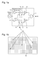
- FIG. 1a depicts a block diagram of a clock detector 10 being based on two mono-flops 12, 13 detecting under frequency conditions, for example ⁇ 1 MHz.
- Mono-flop 12 monitors clock low state duration and the other mono-flop 13 monitors one clock high state duration.
- clock low state duration is longer than the mono-flop delay of mono-flop 12 - together with node full discharge transistor 18 - and an alarm event is generated by Schmitt trigger 14 and propagated to output 20 through gate 11, which is for example a NAND gate.
- clock high state duration is longer than mono-flop delay of mono-flop 13 - together with node full discharge transistor 19 - an alarm event is generated by Schmitt trigger 15 and propagated to output 20 through gate 11.
- the mono-flop delay is defined by buffer output drive capability and integrated C capacitor values 16 and 17 respectively for clock low duration state and clock high duration state.
- the clock detector 10 can monitor frequency and duty cycle parameters of the clock signal. In case of a deviation of either frequency or of duty cycle parameters an alarm «clock tamper detected» 20 is generated.
- the proposed clock detector 10 has a complexity similar to other standard cells of a digital unit, since the clock detector 10 is concealed a standard cell, that is as flip-flop unit. This allows on preventing any external manipulation as well as an effective hiding of these clock detectors 10 within an integrated circuit.
- the term standard cell comprises a set of transistors interconnected together to implement Boolean or storage logic function between input(s) and output(s). The layout of this cell is formatted in a way that cells could assemble into an array to build more complex function in a compact manner.
- Clock detector 10 can be effectively layout as set of transistors with interconnections.
- the clock detector 10 as disclosed above is not dependent of other clock signals (which might be also be tampered), since the characteristics of the clock are mapped in the specific parameters for the components as mono-flop 12, 13, the Schmitt trigger 14, 15 and the others. This is a considerable advantage.
- Figure 1b depicts the principle of an arrangement of a plurality of clock detectors 10 in an integrated circuit 30.
- the clock detectors 10 are placed in the integrated circuit at specific locations respectively at critical points for protecting for example a specific cell or register, a specific function or a group of specific functions.
- the outputs 20 with the alarm «clock tamper detected» 20 of the clock detectors 10 are connected with a clock detector network (not explicitly shown in the drawings) generating an alarm, when only one clock detector 10 monitors a deviation of the clock.
- FIG. 2 depicts a more sophisticated circuit configuration.
- a protection of an integrated circuit 30 is reached with a plurality of clock detectors 10 in a so called clock tree topology.
- the clock detectors 10 are functionally placed at different levels. This allows a specific detection of an external manipulation of the clock.
- the levels can be defined as:
- the outputs 20 with the alarm «clock tamper detected» 20 of the clock detectors 10 are connected with a clock detector network according to their assigned level. This allows a generation of a level specific alarm «clock tamper detected».
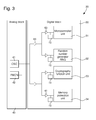
- the integrated circuit 30 includes in a general manner an analog block 40 connected to a digital block 50 comprising several digital units 51, 52, 53, 54 each with at least one clock detector 10.
- the digital block 50 can comprise a microcontroller unit 51, a random number generator RNG 52, a cryptography function unit 53 and a memory protection unit 54.
- an oscillator 41 for supplying signal clock CLK for several digital units of the digital block 50, and a cell 42 for frequency monitoring FMON of the oscillator signal characteristics.
- a level of protection of the integrated circuit can be defeated by neutralizing FMON in particular from external manipulation.
- Said frequency monitoring cell verifies that the signal frequency delivered by OSC oscillator 41 is within frequency monitoring limits defined by security architect. This is the typical organization, we will find commonly implemented in secure IC having such frequency monitoring security function.
- the clock signal generated by the oscillator 41 is supplied to several digital units from the digital block 50 for example through amplifier buffers 60 not inverters in order to clock different operations in the digital block 50.
- amplifier buffers 60 not inverters With this arrangement as a tree topology having different functional levels, it is possible to verify bufferized clock signal closer to the use point. So the effort to locate and to recognize the different clock detectors 10 and to neutralize them with an external manipulation becomes extremely difficult.
- This configuration allows for guaranteeing a good security of the integrated circuit and for improving the protection coverage by making immune clock detectors to neutralization attempts.
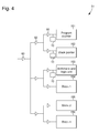
- FIG. 4 shows the different components of the microcontroller unit 51 in the digital block of the integrated circuit.
- the microcontroller unit 51 includes a program counter 151, a stack pointer 152, an arithmetic and logic unit 153 and a set of n blocks, which are shown by the first block 154, the second block 155 and the n th block 156.
- No clock detectors 10 are provided for the set of n blocks given that they are non-vulnerable blocks.
- FIG. 5 shows the different components of the random number generator RNG 52 in the digital block of the integrated circuit.
- Said random number generator RNG 52 are shown with a set of n flip-flops.
- a specific clock detector 10 is placed at each input of the different flip-flops.
- FIG 6 shows the different components of the cryptography function unit 53 in the digital block of the integrated circuit.
- Said cryptography function unit 53 can include a first flip-flop crypto 351, a second flip-flop crypto 352, a first key storage flip-flop 353, a second key storage flip-flop 354 or other, a third flip-flop crypto 355 and a fourth flip-flop crypto 356.
- a clock detector For the security architect aware about fault attacks, it can be provided to place a clock detector at input of first flip-flop crypto 351, second flip-flop crypto 352, first key storage flip-flop 353, and second key storage flip-flop 354.
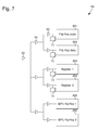
- FIG 7 shows the different components of the memory protection unit 54 in the digital block of the integrated circuit.
- Said memory protection unit 54 can include a flip-flop code 451, a flip-flop data 452, a first register 453, a second register 454, a first MPU flip-flop 455 and a second MPU flip-flop 456.
- a clock detector 10 By considering the memory protection unit security function in order to protect said circuit against illegal memory access, it is important to place a clock detector 10 at each input of flip-flop code 451, flip-flop data 452, first register 453 and a second register 454.
- the invention is not limited to clock detectors 10 as disclosed above. Clock detectors 10 with other components as disclosed above could be also envisaged. However it is important, that the complexity of the clock detector 10 remains comparable to the other cells in particular of a digital unit in digital clock of the integrated circuit.
Landscapes
- Engineering & Computer Science (AREA)
- Physics & Mathematics (AREA)
- General Engineering & Computer Science (AREA)
- Computer Security & Cryptography (AREA)
- General Physics & Mathematics (AREA)
- Computer Hardware Design (AREA)
- Theoretical Computer Science (AREA)
- Software Systems (AREA)
- Mathematical Physics (AREA)
- Computing Systems (AREA)
- Semiconductor Integrated Circuits (AREA)
- Manipulation Of Pulses (AREA)
Abstract
Description
- The present invention relates to a circuit configuration for detecting external manipulation of the clock in an integrated circuit. The integrated circuit comprises digital units and at least one clock detector monitoring frequency and duty cycle parameters of a clock signal. In case of a deviation of either frequency or of a duty cycle parameter an alarm signal can be generated at the output of said at least one clock detector.
- The present invention further relates to a method for detecting an external manipulation of the clock in a circuit configuration.
- Integrated circuits developed for secure application usually embed internal frequency detector to prevent from external manipulation of the internal clock using probing techniques. Main threat addressed by such security mechanism is a clock stepping attack to get control for example of CPU operations or of crypto processor engine.
- The patent
US 7,106,091 B2 discloses the principle of a detector circuit in an integrated circuit. The dedicated detector circuit monitors the interconnect functioning of signal lines between two circuit blocks. The circuit configuration for detecting an unwanted attack on an integrated circuit has a signal line to which a clock signal is applied and at least one line pair which is respectively used to code a bit. The signal line and the at least one line pair are connected between a first and a second circuit blocks in the integrated circuit. The detector circuit changes the operating sequence in the integrated circuit on the basis of the signals on the signal line and on the at least one line pair. The detector circuit can be used to the same extent to test for production faults. - The deficiencies and drawbacks of the known solutions against such threats can be summarized below. So typical properties respectively deficiencies of a clock detector integration include:
- frequency detection cell is usually easy to locate and to modify, as explained in the patent
US 7,106,091 B2 ; - frequency detection interconnections are usually easy to locate and to modify, as explained in the patent
US 7,106,091 B2 ; - frequency detection relies on single analog cell that can be easily neutralized as explained in the patent
US 7,106,091 B2 ; - frequency detection is usually sensing one point to check clock characteristics;
- frequency detection does not check the clock at critical points where signal is used (leaf cells of clock tree);
- frequency detector proposes usually global protection not covering locally critical points, as explained in the patent
US 7,106,091 B2 ; - frequency detection does not embed self-test function to detect any tampering of the monitoring system.
- Further typical properties, respectively deficiencies of a clock detector include:
- frequency detection verifies clock frequency within two limits UFD and OFD but usually not clock characteristic such as duty cycle and
- frequency detection is usually dependent of current sources or other clock signals that could be influenced.
- Generally with an internal frequency detector in an analogue part of the integrated circuit, it is easy to detect the interconnection of said detector and to bypass said detector in order to clock externally from the integrated circuit some operations of the CPU.
- We can cite the patent application
US 2003/0115503 A1 , which describes a system for enhancing fault tolerance and security of a computing system. It is provided a detection of a clock signal between several system clocks and secure clocks in case of fault detections or events of the type over or under frequency detection. This is described in particular concerning the fault tolerance of the electronic system in case of fault detection, but not to make immune each clock detector to neutralization attempts from external manipulation. - In the patent application
WO 00/45244 A1 - The main purpose of invention is to rethink the integration of clock detectors into secure IC design to improve protection coverage and to make IC clock detectors immune to neutralization attempts.
- The task of the present invention is to provide a circuit configuration for detecting external manipulation of the clock by clock detectors. The detectors should not be easily detectable by reverse engineering and the clock detectors should be located at critical points of an integrated circuit in order to effectively and immediately monitor an external manipulation of the clock. Critical points are defined as vulnerable nets of clock network that could be controlled by an attacker to lead a security attack. Said critical points are integrated in the integrated circuit structure of at least one portion of a digital unit, which is clocked by a clock signal from an analog block. A security attack is defined as scenario where sensitive information host into integrated circuit is manipulated or disclosed.
- This aim is reached by a circuit configuration specified with the features in
claim 1, and a method specified with the features in claim 8. - A circuit configuration is for detecting external manipulation of the clock in an integrated circuit comprising at least one clock detector monitoring frequency and duty cycle parameters of a clock signal, where in case of a deviation of either frequency or of duty cycle parameters an alarm signal is generated. A plurality of said clock detectors is placed at functionally critical points of the integrated circuit and the clock detectors are concealed as standard cells in said integrated circuit. This circuit configuration provides the following advantages:
- i) The invention is based on a furtive respectively concealed multi-point sensing circuitry monitoring globally and locally clock distribution and eventually other sensitive signals.
- ii) Efficiency of these security mechanisms can be reinforced with a method for a periodical and/or automatic verification of the clock detector network integrity generating on purpose controlled clock stop events. Those objectives can be achieved by sensing outputs of clock detectors instantiated to verify clock stop event detection and propagation,. This method provides an effective self-test function of integrity of clock tampering detection circuitry.
- iii) Detection cell shall be layout to appear as flip-flop cell for example having similar complexity (# number of transistors) compared to the other cells in said integrated digital circuit. Verification of the clock detector network integrity can be achieved periodically by stopping voluntary clock (idle mode entry) and verifying using that all detectors raised an alarm.
- In the following, at least one embodiment of a circuit configuration for detecting external manipulation of the internal clock and a method for detecting an external manipulation of the clock in the circuit configuration will be described by making reference to the drawings, in which:
-
Figure 1 a shows a block diagram of a single clock detector; -
Figure 1 b £ schematically shows an arrangement of a plurality of clock detectors in an integrated circuit; -
Figure 2 shows a more sophisticated arrangement of a plurality of clock detectors in an integrated circuit following a clock tree buffering topology; -
Figure 3 shows in more details an example of the arrangement of clock detectors in digital block of an integrated circuit; -
Figure 4 shows an example of the arrangement of clock detectors in portions of a microcontroller unit of the integrated circuit; -
Figure 5 shows an example of the arrangement of clock detectors in portions of a random number generator of the integrated circuit; -
Figure 6 shows an example of the arrangement of clock detectors in portions of a cryptography function unit of the integrated circuit; and -
Figure 7 shows an example of the arrangement of clock detectors in portions of a memory protection unit of the integrated circuit. - Reference is made to
Figure 1a which depicts a block diagram of aclock detector 10 being based on two mono-flops flop 12 monitors clock low state duration and the other mono-flop 13 monitors one clock high state duration. In case clock low state duration is longer than the mono-flop delay of mono-flop 12 - together with node full discharge transistor 18 - and an alarm event is generated by Schmitt trigger 14 and propagated to output 20 throughgate 11, which is for example a NAND gate. In case clock high state duration is longer than mono-flop delay of mono-flop 13 - together with node full discharge transistor 19 - an alarm event is generated bySchmitt trigger 15 and propagated tooutput 20 throughgate 11. - The mono-flop delay is defined by buffer output drive capability and integrated C capacitor values 16 and 17 respectively for clock low duration state and clock high duration state. By this manner the
clock detector 10 can monitor frequency and duty cycle parameters of the clock signal. In case of a deviation of either frequency or of duty cycle parameters an alarm «clock tamper detected» 20 is generated. - It can be easily derived that the proposed
clock detector 10 has a complexity similar to other standard cells of a digital unit, since theclock detector 10 is concealed a standard cell, that is as flip-flop unit. This allows on preventing any external manipulation as well as an effective hiding of theseclock detectors 10 within an integrated circuit. In this context the term standard cell comprises a set of transistors interconnected together to implement Boolean or storage logic function between input(s) and output(s). The layout of this cell is formatted in a way that cells could assemble into an array to build more complex function in a compact manner.Clock detector 10 can be effectively layout as set of transistors with interconnections. - The
clock detector 10 as disclosed above is not dependent of other clock signals (which might be also be tampered), since the characteristics of the clock are mapped in the specific parameters for the components as mono-flop Schmitt trigger -
Figure 1b depicts the principle of an arrangement of a plurality ofclock detectors 10 in anintegrated circuit 30. Theclock detectors 10 are placed in the integrated circuit at specific locations respectively at critical points for protecting for example a specific cell or register, a specific function or a group of specific functions. - The
outputs 20 with the alarm «clock tamper detected» 20 of theclock detectors 10 are connected with a clock detector network (not explicitly shown in the drawings) generating an alarm, when only oneclock detector 10 monitors a deviation of the clock. -
Figure 2 depicts a more sophisticated circuit configuration. A protection of anintegrated circuit 30 is reached with a plurality ofclock detectors 10 in a so called clock tree topology. Theclock detectors 10 are functionally placed at different levels. This allows a specific detection of an external manipulation of the clock. - The levels can be defined as:
- whole
integrated circuit 30, for example level 0; - specific function as e.g. crypto processor, for
example level 1; - particular register, for
example level 2. - It has to be emphasized, that the local placement of the
detectors 10 within the integrated circuit is completely independent from the placement at different functional levels. Theoutputs 20 with the alarm «clock tamper detected» 20 of theclock detectors 10 are connected with a clock detector network according to their assigned level. This allows a generation of a level specific alarm «clock tamper detected». - As we can see in more details in
Figure 3 , theintegrated circuit 30 includes in a general manner ananalog block 40 connected to adigital block 50 comprising severaldigital units clock detector 10. Thedigital block 50 can comprise amicrocontroller unit 51, a randomnumber generator RNG 52, acryptography function unit 53 and amemory protection unit 54. - In the
analog block 40, there are anoscillator 41 for supplying signal clock CLK for several digital units of thedigital block 50, and acell 42 for frequency monitoring FMON of the oscillator signal characteristics. Usually said level of protection of the integrated circuit can be defeated by neutralizing FMON in particular from external manipulation. Said frequency monitoring cell verifies that the signal frequency delivered byOSC oscillator 41 is within frequency monitoring limits defined by security architect. This is the typical organization, we will find commonly implemented in secure IC having such frequency monitoring security function. - The clock signal generated by the
oscillator 41 is supplied to several digital units from thedigital block 50 for example throughamplifier buffers 60 not inverters in order to clock different operations in thedigital block 50. With this arrangement as a tree topology having different functional levels, it is possible to verify bufferized clock signal closer to the use point. So the effort to locate and to recognize thedifferent clock detectors 10 and to neutralize them with an external manipulation becomes extremely difficult. This configuration allows for guaranteeing a good security of the integrated circuit and for improving the protection coverage by making immune clock detectors to neutralization attempts. -
Figure 4 shows the different components of themicrocontroller unit 51 in the digital block of the integrated circuit. Themicrocontroller unit 51 includes aprogram counter 151, astack pointer 152, an arithmetic andlogic unit 153 and a set of n blocks, which are shown by thefirst block 154, thesecond block 155 and the nth block 156. There areclock detectors 10 placed at input ofprogram counter 151,stack pointer 152 and arithmetic andlogic unit 153, which are clock monitoring points more vulnerable by security architecture. Noclock detectors 10 are provided for the set of n blocks given that they are non-vulnerable blocks. -
Figure 5 shows the different components of the randomnumber generator RNG 52 in the digital block of the integrated circuit. Said randomnumber generator RNG 52 are shown with a set of n flip-flops. There are shown first flip-flop 251, second flip-flop 252, third flip-flop 253, fourth flip-flop 254, (n-1)th flip-flop 255 and nth flip-flop 256. Aspecific clock detector 10 is placed at each input of the different flip-flops. By considering the low complexity of the flip-flops to be protected, security architecture can envisage to protect all the flip-flops by theclock detectors 10 against any clock manipulation. -
Figure 6 shows the different components of thecryptography function unit 53 in the digital block of the integrated circuit. Saidcryptography function unit 53 can include a first flip-flop crypto 351, a second flip-flop crypto 352, a first key storage flip-flop 353, a second key storage flip-flop 354 or other, a third flip-flop crypto 355 and a fourth flip-flop crypto 356. For the security architect aware about fault attacks, it can be provided to place a clock detector at input of first flip-flop crypto 351, second flip-flop crypto 352, first key storage flip-flop 353, and second key storage flip-flop 354. -
Figure 7 shows the different components of thememory protection unit 54 in the digital block of the integrated circuit. Saidmemory protection unit 54 can include a flip-flop code 451, a flip-flop data 452, afirst register 453, asecond register 454, a first MPU flip-flop 455 and a second MPU flip-flop 456. By considering the memory protection unit security function in order to protect said circuit against illegal memory access, it is important to place aclock detector 10 at each input of flip-flop code 451, flip-flop data 452,first register 453 and asecond register 454. - The invention is not limited to
clock detectors 10 as disclosed above.Clock detectors 10 with other components as disclosed above could be also envisaged. However it is important, that the complexity of theclock detector 10 remains comparable to the other cells in particular of a digital unit in digital clock of the integrated circuit.
Claims (9)
- Circuit configuration for detecting external manipulation of the clock in an integrated circuit (30) comprising digital units and at least one clock detector (10) monitoring frequency and duty cycle parameters of a clock signal, where in case of a deviation of either frequency or of a duty cycle parameter an alarm signal (20) is generated at the output (11) of said at least one clock detector,
characterized in that the circuit configuration has an arrangement of a plurality of said clock detectors (10) at critical points of the integrated circuit (30), said critical points being integrated in at least one portion of a digital unit of a digital block (50), which is clocked by a clock signal from an analog block (40), and
in that the clock detectors (10) are concealed in digital block (50), as standard cells which comprise each a set of transistors interconnected together to implement Boolean or storage logic function in said integrated circuit (30). - Circuit configuration according to claim 1, characterized by the arrangement of at least one clock detector (10) within a digital unit.
- Circuit configuration according to claim 1 or 2, characterized by the clock detector (10) having a complexity similar to other standard cells of a digital unit.
- Circuit configuration according to claim 3, characterized by the clock detector (10) being concealed as a standard cell preferably as a flip-flop unit.
- Circuit configuration according to any one of claims 1 to 4, wherein the outputs (11) with the alarm signal (20) of the clock detectors (10) are connected with a clock detector network in which an alarm is generated, when only one clock detector (10) monitors a deviation of the clock.
- Circuit configuration according to any one of claims 1 to 5, characterized by an arrangement of the clock detectors (10) in a tree topology having different functional levels and wherein the levels are independent from the local placement of the detectors (10) within the integrated circuit (30).
- Circuit configuration according to claim 6, wherein the outputs (11) with the alarm signal (20) of the clock detectors (10) are connected in a clock detector network according to their assigned level in which a level specific alarm is generated, when only one clock detector (10) of a specific level monitors a deviation of the clock.
- Method for detecting external manipulation of the clock in a circuit configuration according to any one of the claims 1 to 7, the circuit configuration in an integrated circuit (30) comprising:- digital units in a digital block (50) and at least one clock detector (10) monitoring frequency and duty cycle parameters of a clock signal from an analog block (40), where in case of a deviation of either frequency or of a duty cycle parameter an alarm signal (20) is generated at the output (11) of said at least one clock detector;- an arrangement of a plurality of said clock detectors (10) at critical points of the integrated circuit (30), said critical points being integrated in at least one portion of a digital unit of the digital block (50), which is clocked by a clock signal from the analog block (40), and the clock detectors (10) being concealed in digital block (50), as standard cells, which comprise each a set of transistors interconnected together to implement Boolean or storage logic function in said integrated circuit (30);- the outputs (11) with the alarm signal (20) of the clock detectors (10) being connected with a clock detector network;
characterized by
a verification of the clock detector network integrity using the alarm signals (20) at the outputs (11). - Method for detecting external manipulation of the clock in a circuit configuration according to claim 8,
wherein
the verification occurs periodically and/or automatically in order to provide a self-test of the circuit configuration.
Priority Applications (1)
| Application Number | Priority Date | Filing Date | Title |
|---|---|---|---|
| EP15177804.0A EP2983103B1 (en) | 2014-08-07 | 2015-07-22 | Integrated circuit with distributed clock tampering detectors |
Applications Claiming Priority (2)
| Application Number | Priority Date | Filing Date | Title |
|---|---|---|---|
| EP14180234.8A EP2983102A1 (en) | 2014-08-07 | 2014-08-07 | Integrated circuit with distributed clock tampering detectors |
| EP15177804.0A EP2983103B1 (en) | 2014-08-07 | 2015-07-22 | Integrated circuit with distributed clock tampering detectors |
Publications (2)
| Publication Number | Publication Date |
|---|---|
| EP2983103A1 true EP2983103A1 (en) | 2016-02-10 |
| EP2983103B1 EP2983103B1 (en) | 2016-12-28 |
Family
ID=51300581
Family Applications (2)
| Application Number | Title | Priority Date | Filing Date |
|---|---|---|---|
| EP14180234.8A Withdrawn EP2983102A1 (en) | 2014-08-07 | 2014-08-07 | Integrated circuit with distributed clock tampering detectors |
| EP15177804.0A Active EP2983103B1 (en) | 2014-08-07 | 2015-07-22 | Integrated circuit with distributed clock tampering detectors |
Family Applications Before (1)
| Application Number | Title | Priority Date | Filing Date |
|---|---|---|---|
| EP14180234.8A Withdrawn EP2983102A1 (en) | 2014-08-07 | 2014-08-07 | Integrated circuit with distributed clock tampering detectors |
Country Status (2)
| Country | Link |
|---|---|
| US (1) | US9506981B2 (en) |
| EP (2) | EP2983102A1 (en) |
Cited By (1)
| Publication number | Priority date | Publication date | Assignee | Title |
|---|---|---|---|---|
| US20160041226A1 (en) * | 2014-08-07 | 2016-02-11 | Em Microelectronic-Marin Sa | Integrated circuit with distributed clock tampering detectors |
Families Citing this family (2)
| Publication number | Priority date | Publication date | Assignee | Title |
|---|---|---|---|---|
| WO2017062735A1 (en) * | 2015-10-08 | 2017-04-13 | President And Fellows Of Harvard College | Ultrahigh resolution dynamic ic chip activity detection for hardware security |
| GB2603549B (en) * | 2021-05-21 | 2023-03-15 | Nordic Semiconductor Asa | Physical security protection for integrated circuits |
Citations (3)
| Publication number | Priority date | Publication date | Assignee | Title |
|---|---|---|---|---|
| WO2000045244A1 (en) | 1999-02-01 | 2000-08-03 | Koninklijke Philipps Electronics N.V. | Integration of security modules on an integrated circuit |
| US20030115503A1 (en) | 2001-12-14 | 2003-06-19 | Koninklijke Philips Electronics N.V. | System for enhancing fault tolerance and security of a computing system |
| US7106091B2 (en) | 2000-09-11 | 2006-09-12 | Infineon Technologies Ag | Circuit configuration and method for detecting an unwanted attack on an integrated circuit |
Family Cites Families (4)
| Publication number | Priority date | Publication date | Assignee | Title |
|---|---|---|---|---|
| US5898711A (en) * | 1997-05-15 | 1999-04-27 | Vlsi Technology, Inc. | Single event upset detection and protection in an integrated circuit |
| US6535988B1 (en) * | 1999-09-29 | 2003-03-18 | Intel Corporation | System for detecting over-clocking uses a reference signal thereafter preventing over-clocking by reducing clock rate |
| US7076802B2 (en) * | 2002-12-31 | 2006-07-11 | Intel Corporation | Trusted system clock |
| EP2983102A1 (en) * | 2014-08-07 | 2016-02-10 | EM Microelectronic-Marin SA | Integrated circuit with distributed clock tampering detectors |
-
2014
- 2014-08-07 EP EP14180234.8A patent/EP2983102A1/en not_active Withdrawn
-
2015
- 2015-07-22 EP EP15177804.0A patent/EP2983103B1/en active Active
- 2015-08-03 US US14/816,453 patent/US9506981B2/en active Active
Patent Citations (3)
| Publication number | Priority date | Publication date | Assignee | Title |
|---|---|---|---|---|
| WO2000045244A1 (en) | 1999-02-01 | 2000-08-03 | Koninklijke Philipps Electronics N.V. | Integration of security modules on an integrated circuit |
| US7106091B2 (en) | 2000-09-11 | 2006-09-12 | Infineon Technologies Ag | Circuit configuration and method for detecting an unwanted attack on an integrated circuit |
| US20030115503A1 (en) | 2001-12-14 | 2003-06-19 | Koninklijke Philips Electronics N.V. | System for enhancing fault tolerance and security of a computing system |
Cited By (2)
| Publication number | Priority date | Publication date | Assignee | Title |
|---|---|---|---|---|
| US20160041226A1 (en) * | 2014-08-07 | 2016-02-11 | Em Microelectronic-Marin Sa | Integrated circuit with distributed clock tampering detectors |
| US9506981B2 (en) * | 2014-08-07 | 2016-11-29 | Em Microelectronic-Marin S.A. | Integrated circuit with distributed clock tampering detectors |
Also Published As
| Publication number | Publication date |
|---|---|
| US9506981B2 (en) | 2016-11-29 |
| US20160041226A1 (en) | 2016-02-11 |
| EP2983102A1 (en) | 2016-02-10 |
| EP2983103B1 (en) | 2016-12-28 |
Similar Documents
| Publication | Publication Date | Title |
|---|---|---|
| Schellenberg et al. | An inside job: Remote power analysis attacks on FPGAs | |
| Yuce et al. | Fault attacks on secure embedded software: Threats, design, and evaluation | |
| Yang et al. | A2: Analog malicious hardware | |
| Karri et al. | Trustworthy hardware: Identifying and classifying hardware trojans | |
| US9523736B2 (en) | Detection of fault injection attacks using high-fanout networks | |
| Zick et al. | Sensing nanosecond-scale voltage attacks and natural transients in FPGAs | |
| Gnad et al. | Voltage-based covert channels using FPGAs | |
| Mal-Sarkar et al. | Hardware trojan attacks in fpga devices: threat analysis and effective counter measures | |
| Chakraborty et al. | On-demand transparency for improving hardware Trojan detectability | |
| US7590880B1 (en) | Circuitry and method for detecting and protecting against over-clocking attacks | |
| US9037895B2 (en) | System and methods for silencing hardware backdoors | |
| EP1252561B1 (en) | Microprocessor resistant to power analysis | |
| Deng et al. | Novel design strategy toward a2 trojan detection based on built-in acceleration structure | |
| US9397663B2 (en) | Fault protection for high-fanout signal distribution circuitry | |
| Saß et al. | Oops..! I Glitched It Again! How to {Multi-Glitch} the {Glitching-Protections} on {ARM}{TrustZone-M} | |
| Gnad et al. | Remote electrical-level security threats to multi-tenant FPGAs | |
| Al-Anwar et al. | Hardware Trojan detection methodology for FPGA | |
| EP2983103B1 (en) | Integrated circuit with distributed clock tampering detectors | |
| Guilley et al. | Fault injection resilience | |
| Islam et al. | Pmu-trojan: on exploiting power management side channel for information leakage | |
| Chaudhuri et al. | Hacking the fabric: Targeting partial reconfiguration for fault injection in FPGA fabrics | |
| Diktopoulos et al. | Assessing the effectiveness of active fences against SCAs for multi-tenant FPGAs | |
| Galathy et al. | A systematic approach to fault attack resistant design | |
| Kaur et al. | Analytical classifications of side channel attacks, glitch attacks and fault injection techniques: their countermeasures | |
| US20240386145A1 (en) | Physical security protection for integrated circuits |
Legal Events
| Date | Code | Title | Description |
|---|---|---|---|
| PUAI | Public reference made under article 153(3) epc to a published international application that has entered the european phase |
Free format text: ORIGINAL CODE: 0009012 |
|
| AK | Designated contracting states |
Kind code of ref document: A1 Designated state(s): AL AT BE BG CH CY CZ DE DK EE ES FI FR GB GR HR HU IE IS IT LI LT LU LV MC MK MT NL NO PL PT RO RS SE SI SK SM TR |
|
| AX | Request for extension of the european patent |
Extension state: BA ME |
|
| 17P | Request for examination filed |
Effective date: 20160810 |
|
| RBV | Designated contracting states (corrected) |
Designated state(s): AL AT BE BG CH CY CZ DE DK EE ES FI FR GB GR HR HU IE IS IT LI LT LU LV MC MK MT NL NO PL PT RO RS SE SI SK SM TR |
|
| GRAJ | Information related to disapproval of communication of intention to grant by the applicant or resumption of examination proceedings by the epo deleted |
Free format text: ORIGINAL CODE: EPIDOSDIGR1 |
|
| GRAP | Despatch of communication of intention to grant a patent |
Free format text: ORIGINAL CODE: EPIDOSNIGR1 |
|
| RIC1 | Information provided on ipc code assigned before grant |
Ipc: G06F 21/75 20130101ALI20160923BHEP Ipc: H03K 19/003 20060101ALI20160923BHEP Ipc: G06F 21/55 20130101AFI20160923BHEP |
|
| GRAS | Grant fee paid |
Free format text: ORIGINAL CODE: EPIDOSNIGR3 |
|
| INTG | Intention to grant announced |
Effective date: 20161024 |
|
| GRAA | (expected) grant |
Free format text: ORIGINAL CODE: 0009210 |
|
| AK | Designated contracting states |
Kind code of ref document: B1 Designated state(s): AL AT BE BG CH CY CZ DE DK EE ES FI FR GB GR HR HU IE IS IT LI LT LU LV MC MK MT NL NO PL PT RO RS SE SI SK SM TR |
|
| REG | Reference to a national code |
Ref country code: GB Ref legal event code: FG4D |
|
| REG | Reference to a national code |
Ref country code: CH Ref legal event code: EP |
|
| REG | Reference to a national code |
Ref country code: AT Ref legal event code: REF Ref document number: 857868 Country of ref document: AT Kind code of ref document: T Effective date: 20170115 |
|
| REG | Reference to a national code |
Ref country code: IE Ref legal event code: FG4D |
|
| REG | Reference to a national code |
Ref country code: CH Ref legal event code: NV Representative=s name: ICB INGENIEURS CONSEILS EN BREVETS SA, CH |
|
| REG | Reference to a national code |
Ref country code: DE Ref legal event code: R096 Ref document number: 602015001133 Country of ref document: DE |
|
| PG25 | Lapsed in a contracting state [announced via postgrant information from national office to epo] |
Ref country code: LV Free format text: LAPSE BECAUSE OF FAILURE TO SUBMIT A TRANSLATION OF THE DESCRIPTION OR TO PAY THE FEE WITHIN THE PRESCRIBED TIME-LIMIT Effective date: 20161228 |
|
| REG | Reference to a national code |
Ref country code: NL Ref legal event code: FP |
|
| REG | Reference to a national code |
Ref country code: LT Ref legal event code: MG4D |
|
| PG25 | Lapsed in a contracting state [announced via postgrant information from national office to epo] |
Ref country code: LT Free format text: LAPSE BECAUSE OF FAILURE TO SUBMIT A TRANSLATION OF THE DESCRIPTION OR TO PAY THE FEE WITHIN THE PRESCRIBED TIME-LIMIT Effective date: 20161228 Ref country code: SE Free format text: LAPSE BECAUSE OF FAILURE TO SUBMIT A TRANSLATION OF THE DESCRIPTION OR TO PAY THE FEE WITHIN THE PRESCRIBED TIME-LIMIT Effective date: 20161228 Ref country code: NO Free format text: LAPSE BECAUSE OF FAILURE TO SUBMIT A TRANSLATION OF THE DESCRIPTION OR TO PAY THE FEE WITHIN THE PRESCRIBED TIME-LIMIT Effective date: 20170328 Ref country code: GR Free format text: LAPSE BECAUSE OF FAILURE TO SUBMIT A TRANSLATION OF THE DESCRIPTION OR TO PAY THE FEE WITHIN THE PRESCRIBED TIME-LIMIT Effective date: 20170329 |
|
| PG25 | Lapsed in a contracting state [announced via postgrant information from national office to epo] |
Ref country code: HR Free format text: LAPSE BECAUSE OF FAILURE TO SUBMIT A TRANSLATION OF THE DESCRIPTION OR TO PAY THE FEE WITHIN THE PRESCRIBED TIME-LIMIT Effective date: 20161228 Ref country code: FI Free format text: LAPSE BECAUSE OF FAILURE TO SUBMIT A TRANSLATION OF THE DESCRIPTION OR TO PAY THE FEE WITHIN THE PRESCRIBED TIME-LIMIT Effective date: 20161228 Ref country code: RS Free format text: LAPSE BECAUSE OF FAILURE TO SUBMIT A TRANSLATION OF THE DESCRIPTION OR TO PAY THE FEE WITHIN THE PRESCRIBED TIME-LIMIT Effective date: 20161228 |
|
| REG | Reference to a national code |
Ref country code: FR Ref legal event code: PLFP Year of fee payment: 3 |
|
| PG25 | Lapsed in a contracting state [announced via postgrant information from national office to epo] |
Ref country code: SK Free format text: LAPSE BECAUSE OF FAILURE TO SUBMIT A TRANSLATION OF THE DESCRIPTION OR TO PAY THE FEE WITHIN THE PRESCRIBED TIME-LIMIT Effective date: 20161228 Ref country code: RO Free format text: LAPSE BECAUSE OF FAILURE TO SUBMIT A TRANSLATION OF THE DESCRIPTION OR TO PAY THE FEE WITHIN THE PRESCRIBED TIME-LIMIT Effective date: 20161228 Ref country code: IS Free format text: LAPSE BECAUSE OF FAILURE TO SUBMIT A TRANSLATION OF THE DESCRIPTION OR TO PAY THE FEE WITHIN THE PRESCRIBED TIME-LIMIT Effective date: 20170428 Ref country code: EE Free format text: LAPSE BECAUSE OF FAILURE TO SUBMIT A TRANSLATION OF THE DESCRIPTION OR TO PAY THE FEE WITHIN THE PRESCRIBED TIME-LIMIT Effective date: 20161228 Ref country code: CZ Free format text: LAPSE BECAUSE OF FAILURE TO SUBMIT A TRANSLATION OF THE DESCRIPTION OR TO PAY THE FEE WITHIN THE PRESCRIBED TIME-LIMIT Effective date: 20161228 |
|
| PG25 | Lapsed in a contracting state [announced via postgrant information from national office to epo] |
Ref country code: BG Free format text: LAPSE BECAUSE OF FAILURE TO SUBMIT A TRANSLATION OF THE DESCRIPTION OR TO PAY THE FEE WITHIN THE PRESCRIBED TIME-LIMIT Effective date: 20170328 Ref country code: BE Free format text: LAPSE BECAUSE OF FAILURE TO SUBMIT A TRANSLATION OF THE DESCRIPTION OR TO PAY THE FEE WITHIN THE PRESCRIBED TIME-LIMIT Effective date: 20161228 Ref country code: SM Free format text: LAPSE BECAUSE OF FAILURE TO SUBMIT A TRANSLATION OF THE DESCRIPTION OR TO PAY THE FEE WITHIN THE PRESCRIBED TIME-LIMIT Effective date: 20161228 Ref country code: IT Free format text: LAPSE BECAUSE OF FAILURE TO SUBMIT A TRANSLATION OF THE DESCRIPTION OR TO PAY THE FEE WITHIN THE PRESCRIBED TIME-LIMIT Effective date: 20161228 Ref country code: PL Free format text: LAPSE BECAUSE OF FAILURE TO SUBMIT A TRANSLATION OF THE DESCRIPTION OR TO PAY THE FEE WITHIN THE PRESCRIBED TIME-LIMIT Effective date: 20161228 Ref country code: ES Free format text: LAPSE BECAUSE OF FAILURE TO SUBMIT A TRANSLATION OF THE DESCRIPTION OR TO PAY THE FEE WITHIN THE PRESCRIBED TIME-LIMIT Effective date: 20161228 Ref country code: PT Free format text: LAPSE BECAUSE OF FAILURE TO SUBMIT A TRANSLATION OF THE DESCRIPTION OR TO PAY THE FEE WITHIN THE PRESCRIBED TIME-LIMIT Effective date: 20170428 |
|
| REG | Reference to a national code |
Ref country code: DE Ref legal event code: R097 Ref document number: 602015001133 Country of ref document: DE |
|
| PLBE | No opposition filed within time limit |
Free format text: ORIGINAL CODE: 0009261 |
|
| STAA | Information on the status of an ep patent application or granted ep patent |
Free format text: STATUS: NO OPPOSITION FILED WITHIN TIME LIMIT |
|
| PG25 | Lapsed in a contracting state [announced via postgrant information from national office to epo] |
Ref country code: DK Free format text: LAPSE BECAUSE OF FAILURE TO SUBMIT A TRANSLATION OF THE DESCRIPTION OR TO PAY THE FEE WITHIN THE PRESCRIBED TIME-LIMIT Effective date: 20161228 |
|
| 26N | No opposition filed |
Effective date: 20170929 |
|
| PG25 | Lapsed in a contracting state [announced via postgrant information from national office to epo] |
Ref country code: SI Free format text: LAPSE BECAUSE OF FAILURE TO SUBMIT A TRANSLATION OF THE DESCRIPTION OR TO PAY THE FEE WITHIN THE PRESCRIBED TIME-LIMIT Effective date: 20161228 |
|
| REG | Reference to a national code |
Ref country code: IE Ref legal event code: MM4A |
|
| PG25 | Lapsed in a contracting state [announced via postgrant information from national office to epo] |
Ref country code: IE Free format text: LAPSE BECAUSE OF NON-PAYMENT OF DUE FEES Effective date: 20170722 |
|
| REG | Reference to a national code |
Ref country code: FR Ref legal event code: PLFP Year of fee payment: 4 |
|
| PG25 | Lapsed in a contracting state [announced via postgrant information from national office to epo] |
Ref country code: LU Free format text: LAPSE BECAUSE OF NON-PAYMENT OF DUE FEES Effective date: 20170722 |
|
| PG25 | Lapsed in a contracting state [announced via postgrant information from national office to epo] |
Ref country code: MT Free format text: LAPSE BECAUSE OF NON-PAYMENT OF DUE FEES Effective date: 20170722 |
|
| REG | Reference to a national code |
Ref country code: AT Ref legal event code: UEP Ref document number: 857868 Country of ref document: AT Kind code of ref document: T Effective date: 20161228 |
|
| PG25 | Lapsed in a contracting state [announced via postgrant information from national office to epo] |
Ref country code: MC Free format text: LAPSE BECAUSE OF FAILURE TO SUBMIT A TRANSLATION OF THE DESCRIPTION OR TO PAY THE FEE WITHIN THE PRESCRIBED TIME-LIMIT Effective date: 20161228 Ref country code: HU Free format text: LAPSE BECAUSE OF FAILURE TO SUBMIT A TRANSLATION OF THE DESCRIPTION OR TO PAY THE FEE WITHIN THE PRESCRIBED TIME-LIMIT; INVALID AB INITIO Effective date: 20150722 |
|
| PG25 | Lapsed in a contracting state [announced via postgrant information from national office to epo] |
Ref country code: CY Free format text: LAPSE BECAUSE OF FAILURE TO SUBMIT A TRANSLATION OF THE DESCRIPTION OR TO PAY THE FEE WITHIN THE PRESCRIBED TIME-LIMIT Effective date: 20161228 |
|
| PG25 | Lapsed in a contracting state [announced via postgrant information from national office to epo] |
Ref country code: MK Free format text: LAPSE BECAUSE OF FAILURE TO SUBMIT A TRANSLATION OF THE DESCRIPTION OR TO PAY THE FEE WITHIN THE PRESCRIBED TIME-LIMIT Effective date: 20161228 |
|
| GBPC | Gb: european patent ceased through non-payment of renewal fee |
Effective date: 20190722 |
|
| PG25 | Lapsed in a contracting state [announced via postgrant information from national office to epo] |
Ref country code: TR Free format text: LAPSE BECAUSE OF FAILURE TO SUBMIT A TRANSLATION OF THE DESCRIPTION OR TO PAY THE FEE WITHIN THE PRESCRIBED TIME-LIMIT Effective date: 20161228 |
|
| PG25 | Lapsed in a contracting state [announced via postgrant information from national office to epo] |
Ref country code: GB Free format text: LAPSE BECAUSE OF NON-PAYMENT OF DUE FEES Effective date: 20190722 |
|
| PG25 | Lapsed in a contracting state [announced via postgrant information from national office to epo] |
Ref country code: AL Free format text: LAPSE BECAUSE OF FAILURE TO SUBMIT A TRANSLATION OF THE DESCRIPTION OR TO PAY THE FEE WITHIN THE PRESCRIBED TIME-LIMIT Effective date: 20161228 |
|
| P01 | Opt-out of the competence of the unified patent court (upc) registered |
Effective date: 20230611 |
|
| PGFP | Annual fee paid to national office [announced via postgrant information from national office to epo] |
Ref country code: NL Payment date: 20250620 Year of fee payment: 11 |
|
| PGFP | Annual fee paid to national office [announced via postgrant information from national office to epo] |
Ref country code: FR Payment date: 20250620 Year of fee payment: 11 |
|
| PGFP | Annual fee paid to national office [announced via postgrant information from national office to epo] |
Ref country code: DE Payment date: 20250620 Year of fee payment: 11 |
|
| PGFP | Annual fee paid to national office [announced via postgrant information from national office to epo] |
Ref country code: AT Payment date: 20250623 Year of fee payment: 11 |
|
| PGFP | Annual fee paid to national office [announced via postgrant information from national office to epo] |
Ref country code: CH Payment date: 20250801 Year of fee payment: 11 |