EP2982950A1 - Process of detection of light and associated device - Google Patents
Process of detection of light and associated device Download PDFInfo
- Publication number
- EP2982950A1 EP2982950A1 EP14180354.4A EP14180354A EP2982950A1 EP 2982950 A1 EP2982950 A1 EP 2982950A1 EP 14180354 A EP14180354 A EP 14180354A EP 2982950 A1 EP2982950 A1 EP 2982950A1
- Authority
- EP
- European Patent Office
- Prior art keywords
- dielectric
- light
- detected light
- reference device
- dielectric junction
- Prior art date
- Legal status (The legal status is an assumption and is not a legal conclusion. Google has not performed a legal analysis and makes no representation as to the accuracy of the status listed.)
- Withdrawn
Links
Images







Classifications
-
- G—PHYSICS
- G01—MEASURING; TESTING
- G01J—MEASUREMENT OF INTENSITY, VELOCITY, SPECTRAL CONTENT, POLARISATION, PHASE OR PULSE CHARACTERISTICS OF INFRARED, VISIBLE OR ULTRAVIOLET LIGHT; COLORIMETRY; RADIATION PYROMETRY
- G01J4/00—Measuring polarisation of light
- G01J4/04—Polarimeters using electric detection means
Definitions
- An aspect of the present invention relates to the technical field of light detection.
- Another aspect of the present invention relates to the technical field of light characterization, and in particular to the technical field of the characterization of the polarization of light and its trajectory.
- a photodiode is a semiconductor device that converts incident light into an electric current.
- a photodiode is typically a p-n junction.
- a photodiode typically has dimensions of the order of 10 ⁇ m.
- polarizers are known.
- a polarizer is an optical filter that passes light of a specific polarization and blocks waves of other polarizations: it can convert a beam of light of undefined or mixed polarization into a beam with well-defined polarization.
- a polarizing film may be deposited on a light sensor such as a photodiode, however typically implying a decrease in sensitivity for the light sensor and preventing the light sensor from being downsized.
- a conventional camera captures the projection onto a 2-dimensional plane of a 3-dimensional light-field. The resulting picture is in focus within a given plane but information to recreate a focus within an alternate plane is lost.
- a light-field camera sacrifices resolution in order, thanks to an array of lenses, to capture the orientation of the impinging light by comparing neighbouring regions. The ensuing dataset enables the post-facto redefinition of the focal plane. Due to their implementation, light-field cameras presently suffer from low resolutions. At present, no arrayed solution exists to characterize in multiple dimensions the spatial orientation of the linear polarization of light.
- An objective of the invention is to enable the detection of light using a device at the nanometre scale. Another objective of the invention is to enable the detection of light using a device that can be integrated with a high spatial density. Another objective of the invention is to enable the characterization of the degree to which the detected light is polarized along a first spatial direction, using a device at the nanometre scale. Another objective of the invention is to enable the characterization of the degree to which the detected light is polarized along a first spatial direction and along a second spatial direction, using a device at the nanometre scale. Another objective of the invention is to enable the characterization of the degree to which the detected light is polarized along a first spatial direction, along a second spatial direction and along a third spatial direction, using a device at the nanometre scale.
- Another objective of the invention is to offer an information on the trajectory that light have taken, using a device at the nanometre scale.
- Another objective of the invention is to enable the hardware detection of glare within a picture, and to provide a new hardware implementation for a light-field camera.
- a process of detection of light comprising:
- the presence or the absence of light may be detected using a dielectric junction at the nanometre scale.
- the process of detection of light according to an aspect of the invention may further allow quantifying detected light.
- the process of detection of light according to an aspect of the invention may further allow characterizing the degree to which the detected light is polarized along a first spatial direction.
- the process of detection of light according to an aspect of the invention may further allow characterizing the degree to which the detected light is polarized along a first spatial direction and along a second spatial direction.
- the process of detection of light according to an aspect of the invention may further allow characterizing the degree to which the detected light is polarized along a first spatial direction, along a second spatial direction and along a third spatial direction.
- the process of detection of light according to an aspect of the invention may have one or several complementary characteristics among the following characteristics considered individually or in any technically possible combinations:
- Present implementations of a light-field camera utilize an array of large pixels, preceded by a microlens, in order to gather information on the propagation direction of light.
- An aspect of the present invention also uses a plurality of devices to do so, but each device may advantageously be shrunk to the nanoscale while maintaining sufficient sensitivity. This circumvents a major drawback of present implementations of a light-field camera.
- an aspect of the invention advantageously enables the detection of the polarization vector of light in an arrayed fashion. This is useful for scientific applications, but also consumer applications such as the hardware detection of glare, which is essentially polarized light.
- an image with glare may be optimally processed to reduce this glare without affecting the quality of the image.
- FIG. 1 schematically illustrates a stack 1 according to an embodiment of the invention.
- the stack 1 comprises:
- the dielectric layer D has a thickness w_D that is measured along a direction perpendicular to the first reference plane P1.
- Said thickness w_D may typically be comprised between 1 nanometre and 100 nanometres.
- Said thickness w_D may beneficially be less than or equal to 4 nanometres, and said thickness w_D may in particular beneficially be comprised between 2 nanometres and 3 nanometres, in order to promote a nominally elastic regime of tunnelling transport. In such a nominally elastic regime of tunnelling transport, electrons may tunnel directly from one interface metallic layer/dielectric layer to another interface metallic layer/dielectric layer.
- said thickness w_D may be greater than 4 nanometres. Said thickness w_D may in particular be greater than 10 nanometres.
- the transport of electrons across the dielectric layer is interpreted in terms of hopping transport across the dielectric layer D.
- said thickness range indeed, if localized states within the tunnel barrier's band gap arise due to the presence of structural defects, several tunnelling steps will take place as the electron crosses the barrier by hopping onto defect sites.
- the dielectric layer D may for example comprise a material chosen among the followings:
- Figure 2a schematically illustrates a device 10 for detecting light according to a first embodiment of the invention, said device 10 having a first geometry.
- the device 10 having the first geometry is also referred to as "normal dielectric junction”.
- the device 10 comprises:
- Said FeCoB/MgO/FeCoB dielectric junction may nevertheless exhibit sensitivity to the given wavelength ranges outside of the given ranges of parameters, and notably at and beyond room temperature.
- This table is non-exhaustive in terms of available wavelength ranges.
- said FeCoB/MgO/CoFeB dielectric junction may exhibit sensitivity within 375-500 nanometres, with a 10 mV bias voltage and at room temperature.
- Figure 2b schematically illustrates a device 10' for detecting light according to a second embodiment of the invention, said device 10' having a second geometry.
- the device 10' having the second geometry is also referred to as "lateral dielectric junction”.
- the device 10' comprises:
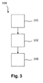
- FIG. 3 schematically illustrates a diagram of the steps of a process 100 of detection of light according to an embodiment of the invention.
- the process 100 comprises the following steps:
- the process 100 may further comprise a step of measuring the polarization of light that may be impinging on the stack 1 of the normal dielectric junction 10 or from the stack 1' of the lateral dielectric junction 10', referred to as "first stack".
- first stack the stack 1 of the normal dielectric junction 10 or from the stack 1' of the lateral dielectric junction 10'
- said step of measuring polarization allows for a relative characterization of light impinging on said stack 1.
- the process 100 may beneficially comprise a second calibration step, wherein:
- Figure 4a schematically illustrates a normal reference device 20 for quantifying detected light that comprises:
- Figure 4b schematically illustrates a lateral reference device 20' for quantifying detected light that comprises:
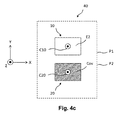
- Figure 4c schematically illustrates a device 40 allowing quantifying the presence or the absence of light, said device 40 comprising:
- Figure 4d schematically illustrates a device 40' allowing quantifying the presence or the absence of light, said device 40' comprising:
- Figure 4d shows that the lateral dielectric junction 10' and the lateral reference device 20' for quantifying detected light are oriented relative to each other in such a way that the second reference plane P2 of the lateral dielectric junction 10' and the second reference plane P2 of the lateral reference device 20' for quantifying detected light are parallel.
- the first reference plane P2 of the lateral dielectric junction 10' and the first reference plane P2 of the lateral reference device 20' for quantifying detected light are merged, that is to say, the lateral dielectric junction 10' and the lateral reference device 20' for quantifying detected light have the same coordinates according the third axis Z.
- the lateral dielectric junction 10' and the lateral reference device 20' for quantifying detected light may have different coordinates according to the third axis Z.
- the only condition here is that the operational characteristics of both the lateral reference device 20' and the lateral dielectric junction 10' in the absence of light impinging on the lateral dielectric junction 10' be identical.
- the first reference plane P1' of the lateral dielectric junction 10' and the first reference plane P1' of the lateral reference device 20' for quantifying detected light are beneficially parallel.
- the device 40' illustrated in figure 4d is adapted both to the case of an isotropic conduction through the dielectric layers D, and to the case of an anisotropic conduction through the dielectric layers D. If the conduction through the dielectric layers D is isotropic, this means that the conduction will be the same regardless of the absolute direction of current propagation.
- the lateral reference device 20' for quantifying detected light may have a current C20' that is not parallel to the current C10' of the lateral dielectric junction 10'. In the case of isotropic conduction, the first reference plane P1' of the lateral dielectric junction 10' and the first reference plane P1' of the lateral reference device 20' for quantifying detected light may be parallel but it is not necessary.
- the conduction through the dielectric layers D is anisotropic, then the conduction will not be the same for two given directions of current propagation through D.
- the lateral reference device 20' has a current C20' that is parallel to the current C10' of the lateral dielectric junction 10'.
- the first reference plane P1' of the lateral dielectric junction 10' and the first reference plane P1' of the lateral reference device 20' for quantifying detected light are parallel.
- Figure 5 schematically illustrates a diagram of the steps of a process 200 of quantification of the presence or the absence of light according to an embodiment of the invention.
- the process 200 typically uses:
- Figure 6a schematically illustrates a normal reference device 30 for characterizing detected light along a first spatial direction that comprises:
- Figure 6c schematically illustrates a device 50 allowing quantifying the presence or the absence of light and characterizing light along a first spatial direction, said device 50 comprising:
- the impact of depolarized light on conduction is isotropic means that conduction does not depend on the orientation of the depolarized light that may be impinging on the normal reference device 30 for characterizing detected light along a first spatial direction.
- the first reference plane P1 of the normal dielectric junction 10, the first reference plane P1 of the normal reference device 20 for quantifying detected light and the first reference plane P1 of the normal reference device 30 for characterizing detected light along a the first spatial direction are merged, that is to say, the normal dielectric junction 10, the normal reference device 20 for quantifying detected light and the normal reference device 30 for characterizing detected light along a the first spatial direction have the same coordinates according the third axis Z.
- the normal dielectric junction 10 the normal reference device 20 for quantifying detected light and the normal reference device 30 for characterizing detected light along a the first spatial direction may have different coordinates according to the third axis Z.
- the normal reference device 20 for quantifying detected light and the normal reference device 30 for characterizing detected light along a the first spatial direction share the same reference plane P1 and are positioned close to one another so that these devices are exposed to the same flux of light.
- the normal dielectric junction 10 the normal reference device 20 for quantifying detected light and the normal reference device 30 for characterizing detected light along a the first spatial direction have the same coordinates according to the first axis X, and different coordinates according to the second axis Y.
- the normal dielectric junction 10, the normal reference device 20 for quantifying detected light and the normal reference device 30 for characterizing detected light along a the first spatial direction may have the same coordinates according to the second axis Y, and different coordinates according to the first axis X.
- the normal dielectric junction 10, the normal reference device 20 for quantifying detected light and the normal reference device 30 for characterizing detected light along a the first spatial direction may have different coordinates according the first axis X and different coordinates according to the second axis Y. While respecting these positioning criteria, the previously described considerations of relative positioning between the normal dielectric junction 10 and the normal reference device 20 that apply for device 40 also apply to the normal dielectric junction 10 and the normal reference device 20 of device 50.
- Figure 6d schematically illustrates a device 50' allowing quantifying the presence or the absence of light and characterizing light along a first spatial direction, said device 50' comprising:
- the first reference plane P1' of the lateral dielectric junction 10' and the first reference plane P1' of the lateral reference device 20' for quantifying detected light may be parallel but it is not necessary.
- Figure 6d further shows that the lateral dielectric junction 10' and the lateral reference device 30' for characterizing detected light along a first spatial direction are oriented relative to each other in such a way that the second reference plane P2 of the lateral dielectric junction 10' and the second reference plane P2 of the lateral reference device 30' for characterizing detected light along a first spatial direction are parallel.
- the first reference plane P1' of the lateral dielectric junction 10' and the first reference plane P1' of the lateral reference device 30' for characterizing detected light along a first spatial direction are beneficially parallel.
- the device 50' illustrated in figure 6d is both adapted to:
- the previously described considerations of relative positioning between the lateral dielectric junction 10' and the lateral reference device 20' that apply for device 40' also apply to the lateral dielectric junction 10' and the lateral reference device 20' of device 50'.
- the lateral reference device 20' for quantifying detected light and the lateral reference device 30' for characterizing detected light along a the first spatial direction share the same reference plane P2 and are positioned close to one another so that these devices are exposed to the same flux of light.
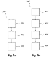
- Figure 7a schematically illustrates a diagram of the steps of a process 300 of characterization of light along a first spatial direction, according to an embodiment of the invention.
- the process 300 typically uses:
- Figure 7b schematically illustrates a diagram of the steps of a process 300' of quantification of the presence or the absence of light and of characterization of light along a first spatial direction, according to an embodiment of the invention.
- the process 300' typically uses:
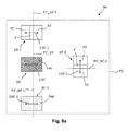
- Figure 8a schematically illustrates a device 60' allowing quantifying the presence or the absence of light and characterizing light along a first spatial direction and along a second spatial direction.
- the device 60' illustrated in figure 8a comprises:
- Figure 8a shows that the first lateral dielectric junction 10'-1 and the lateral reference device 20' for quantifying detected light are oriented relative to each other in such a way that the second reference plane P2 of the first lateral dielectric junction 10'-1 and the second reference plane P2 of the lateral reference device 20' for quantifying detected light are parallel.
- the first reference plane P1'_10'-1 of the first lateral dielectric junction 10'-1 and the first reference plane P1'_20' of the lateral reference device 20' for quantifying detected light are beneficially parallel, but it is not necessary in the case of isotropic conduction through the dielectric layers D.
- Figure 8a further shows that the first lateral dielectric junction 10'-1 and the first lateral reference device 30'-1 for characterizing detected light are oriented relative to each other in such a way that the second reference plane P2 of the first lateral dielectric junction 10'-1 and the second reference plane P2 of the first lateral reference device 30'-1 for characterizing detected light are parallel.
- the first reference plane P1'_10'-1 of the first lateral dielectric junction 10'-1 and the first reference plane P1_30'-1 of the lateral reference device 30'-1 for characterizing detected light are beneficially parallel, but it is not necessary in the case of isotropic conduction through the dielectric layers D.
- the first reference plane P1'_10'-2 of the second lateral dielectric junction 10'-2 is not parallel to the first reference plane P1'_10'-1 of the first lateral dielectric junction 10'-1.
- the first reference plane P1'_10'-2 of the second lateral dielectric junction 10'-2 is beneficially perpendicular to the first reference plane P1'_10'-1 of the first lateral dielectric junction 10'-1.
- Figure 8b schematically illustrates a device 61' allowing quantifying the presence or the absence of light and characterizing light along a first spatial direction and along a second spatial direction, according to a first variant.
- the device 61' according to the first variant illustrated in figure 8b further comprises:
- Figure 8b shows that the second lateral dielectric junction 10'-2 and the second lateral reference device 30'-2 for characterizing detected light are oriented relative to each other in such a way that the second reference plane P2 of the second lateral dielectric junction 10'-2 and the second reference plane P2 of the second lateral reference device 30'-2 for characterizing detected light are parallel.
- Figure 8b also shows that the second lateral dielectric junction 10'-2 and the second lateral reference device 30'-2 for characterizing detected light are oriented relative to each other in such a way that the first reference plane P1'_10'-2 of the second lateral dielectric junction 10'-2 and the first reference plane P1'_30'-2 of the second lateral reference device 30'-2 are parallel, in order to address the case of anisotropic impact of depolarized light on conduction through the dielectric layer D of the second lateral reference device 30'-2 for characterizing detected light.
- the first reference plane P1'_10'-1 of the first lateral dielectric junction 10'-1 and the first reference plane P1'_30'-1 of the lateral reference device 30'-1 for characterizing detected light are beneficially parallel, but it is not necessary in the case of isotropic impact of depolarized light on conduction through the dielectric layer D of the second lateral reference device 30'-2 for characterizing detected light.
- Figure 8c schematically illustrates a device 62' allowing quantifying the presence or the absence of light and characterizing light along a first spatial direction and along a second spatial direction, according to a second variant.
- the device 62' according to the second variant illustrated in figure 8c further comprises:
- Figure 8c shows that the second lateral dielectric junction 10'-2 and the second lateral reference device 20'-2 for quantifying detected light are oriented relative to each other in such a way that the second reference plane P2 of the second lateral dielectric junction 10'-2 and the second reference plane P2 of the second lateral reference device 20'-2 for quantifying detected light are parallel.
- Figure 8c also shows that the second lateral dielectric junction 10'-2 and the second lateral reference device 20'-2 for quantifying detected light are oriented relative to each other in such a way that the first reference plane P1'_10'-2 of the second lateral dielectric junction 10'-2 and the first reference plane P1'_20'-2 of the second lateral reference device 20'-2 are parallel, in order to address the case of anisotropic conduction through the dielectric layers D.
- Figure 9 schematically illustrates a diagram of the steps of a process 400 of quantification of the presence or the absence of light and of characterization of light along a first spatial direction and along a second spatial direction, according to an embodiment of the invention.
- the process 400 may typically use the device 60' illustrated in figure 8a or the device 61' illustrated in figure 8b or the device 62' illustrated in figure 8c .
- the process 400 thus typically uses:
- Figure 10 schematically illustrates a device 70 allowing quantifying the presence or the absence of light and characterizing light along a first spatial direction, along a second spatial direction and along a third spatial direction.
- the device 70 illustrated in figure 10 comprises:
- a three-dimensional polarization vector of light that is to say a three-dimensional vector comprising the degree to which light impinging on the device is polarized along the first, second and third spatial directions, may thus be obtained, allowing one to determine the propagation direction of light.
Landscapes
- Physics & Mathematics (AREA)
- General Physics & Mathematics (AREA)
- Spectroscopy & Molecular Physics (AREA)
- Investigating Or Analysing Materials By Optical Means (AREA)
Abstract
According to an aspect of the invention, it is provided a process of detection of light comprising:
- a step of flowing an electric current through at least a first dielectric junction, said first dielectric junction comprising at least a first metallic layer extending along a first reference plane and a second metallic layer extending parallel to said first reference plane, said first and second metallic layers being separated from each other by a dielectric layer ensuring non-ohmic conduction between said first and second metallic layers;
- a step of measuring the electric resistance of the first dielectric junction;
- a step of determining the presence or the absence of light by using the measured electric resistance of the first dielectric junction. According to another aspect of the invention, it is provided a process of characterization of the degree to which detected light is polarized along a first spatial direction and/or along a second spatial direction and/or along a third spatial direction, using a device at the nanometre scale. This enables the detection of the orientation of the incoming light.
Description
- An aspect of the present invention relates to the technical field of light detection. Another aspect of the present invention relates to the technical field of light characterization, and in particular to the technical field of the characterization of the polarization of light and its trajectory.
- In the technical field of light detection, photodiodes are known. A photodiode is a semiconductor device that converts incident light into an electric current. A photodiode is typically a p-n junction. A photodiode typically has dimensions of the order of 10 µm. There is a need to downsize light sensors.
In the technical field of light polarization characterization, polarizers are known. A polarizer is an optical filter that passes light of a specific polarization and blocks waves of other polarizations: it can convert a beam of light of undefined or mixed polarization into a beam with well-defined polarization.
A polarizing film may be deposited on a light sensor such as a photodiode, however typically implying a decrease in sensitivity for the light sensor and preventing the light sensor from being downsized.
A conventional camera captures the projection onto a 2-dimensional plane of a 3-dimensional light-field. The resulting picture is in focus within a given plane but information to recreate a focus within an alternate plane is lost. A light-field camera sacrifices resolution in order, thanks to an array of lenses, to capture the orientation of the impinging light by comparing neighbouring regions. The ensuing dataset enables the post-facto redefinition of the focal plane. Due to their implementation, light-field cameras presently suffer from low resolutions.
At present, no arrayed solution exists to characterize in multiple dimensions the spatial orientation of the linear polarization of light. - An objective of the invention is to enable the detection of light using a device at the nanometre scale. Another objective of the invention is to enable the detection of light using a device that can be integrated with a high spatial density. Another objective of the invention is to enable the characterization of the degree to which the detected light is polarized along a first spatial direction, using a device at the nanometre scale. Another objective of the invention is to enable the characterization of the degree to which the detected light is polarized along a first spatial direction and along a second spatial direction, using a device at the nanometre scale. Another objective of the invention is to enable the characterization of the degree to which the detected light is polarized along a first spatial direction, along a second spatial direction and along a third spatial direction, using a device at the nanometre scale. Another objective of the invention is to offer an information on the trajectory that light have taken, using a device at the nanometre scale. Another objective of the invention is to enable the hardware detection of glare within a picture, and to provide a new hardware implementation for a light-field camera.
- To this end, according to an aspect of the invention, it is provided a process of detection of light comprising:
- a step of flowing an electric current through at least a first dielectric junction, said first dielectric junction comprising at least a first metallic layer extending along a first reference plane and a second metallic layer extending parallel to said first reference plane, said first and second metallic layers being separated from each other by a dielectric layer ensuring non-ohmic conduction between said first and second metallic layers;
- a step of measuring the electric resistance of the first dielectric junction;
- a step of determining the presence or the absence of light by using the measured electric resistance of the first dielectric junction.
- Thanks to the invention, the presence or the absence of light may be detected using a dielectric junction at the nanometre scale. The process of detection of light according to an aspect of the invention may further allow quantifying detected light. The process of detection of light according to an aspect of the invention may further allow characterizing the degree to which the detected light is polarized along a first spatial direction. The process of detection of light according to an aspect of the invention may further allow characterizing the degree to which the detected light is polarized along a first spatial direction and along a second spatial direction. The process of detection of light according to an aspect of the invention may further allow characterizing the degree to which the detected light is polarized along a first spatial direction, along a second spatial direction and along a third spatial direction.
- Apart from the characteristics mentioned above in the previous paragraph, the process of detection of light according to an aspect of the invention may have one or several complementary characteristics among the following characteristics considered individually or in any technically possible combinations:
- The dielectric layer has a thickness between 0.5 nm and 1000 nm, said thickness being measured along a direction perpendicular to the first reference plane. The dielectric layer preferentially has a thickness between 0.5 nm and 100 nm, said thickness being measured along a direction perpendicular to the first reference plane.
- The dielectric layer has a thickness that is less than or equal to 4 nm, said thickness being measured along a direction perpendicular to the first reference plane.
- The dielectric layer has a thickness between 0.6 and 3 nm, said thickness being measured along a direction perpendicular to the first reference plane.
- The dielectric junction comprises:
- o a substrate extending along a second reference plane, the second reference plane being substantially parallel to the first reference plane;
- o a first electrode extending along the substrate;
- o the first metallic layer extending along the first electrode;
- o the dielectric layer extending along the first metallic layer;
- o the second metallic layer extending along the dielectric layer;
- o a second electrode extending along the second metallic layer.
- Alternatively, the dielectric junction comprises:
- o a substrate extending along a second reference plane, the second reference plane being substantially perpendicular to the first reference plane;
- o a first electrode extending along a plane that is substantially perpendicular to the second reference plane and substantially parallel to the first reference plane,
- o the first metallic layer extending along the first electrode,
- o the dielectric layer extending along the first metallic layer,
- o the second metallic layer extending along the dielectric layer,
- o a second electrode extending along the second metallic layer.
- The dielectric layer is made of magnesium oxide MgO. Alternatively, the dielectric layer may be made of titanium dioxide TiO2, strontium titanate SrTiO3 or aluminium oxide Al2O3. The dielectric layer is beneficially made of a textured dielectric, such as for example a textured oxide. The dielectric layer is preferentially made of an epitaxial dielectric, such as for example an epitaxial oxide. In materials science, the texture of a polycrystalline sample is the distribution of crystallographic orientations of said polycrystalline sample. If the crystallographic orientations are not random but have some preferred orientation along at least one axis, then the sample has a texture. Thanks to this texture or epitaxy, a precise set of atomic orbitals is positioned parallel or perpendicular to the flow of current along a given crystallographic direction. In turn, polarized light shall promote photoelectrons within orbitals that are spatially pointing along the direction of polarization. The asymmetric impact of photoelectrons on current depending on the orbital that they reside in increases the sensitivity of the ensuing device to the degree of polarization of light that is impinging on it.
- A plurality of dielectric junctions is used, said plurality of dielectric junctions comprising at least the first dielectric junction and a reference device for quantifying detected light further comprising an optically opaque cover, the process further comprising:
- o a step of flowing an electric current through said first dielectric junction and through said reference device for quantifying detected light;
- o a step of measuring the electric resistance of said first dielectric junction and of said reference device for quantifying detected light;
- o a step of quantifying the presence or the absence of light around said first dielectric junction by comparing the measured electric resistance of the first dielectric junction with the measured electric resistance of the reference device for quantifying detected light.
- A plurality of dielectric junctions is used, said plurality of dielectric junctions comprising at least the first dielectric junction and a reference device for characterizing detected light further comprising a light depolarizer, the process comprising:
- o a step of flowing an electric current through said first dielectric junction and through said third reference device for characterizing detected light;
- o a step of measuring the electric resistance of said first dielectric junction and of said reference device for characterizing detected light;
- o a step of comparing the measured electric resistance of the first electric junction with the measured electric resistance of the reference device for characterizing detected light, in order to characterize the degree to which light around the first dielectric junction is polarized along a first spatial direction.
- The plurality of dielectric junctions further comprises a reference device for quantifying detected light comprising an optically opaque cover, the process comprising:
- o a step of flowing an electric current through said first dielectric junction, through said reference device for quantifying detected light and through said reference device for characterizing detected light;
- o a step of measuring the electric resistance of the first dielectric junction, of the reference device for quantifying detected light and of the reference device for characterizing detected light;
- o a step of comparing the measured electric resistance of the first dielectric junction with the measured electric resistance of the reference device for quantifying detected light in order to quantify the presence or the absence of light around the first dielectric junction, and
- o a step of comparing the measured electric resistance of the first dielectric junction with the measured electric resistance of the reference device for characterizing detected light in order to characterize the degree to which light around the first dielectric junction is polarized along a first spatial direction.
- The plurality of dielectric junctions further comprises a second dielectric junction, the process comprising:
- o a step of flowing an electric current at least through the first dielectric junction, through the second dielectric junction, through the reference device for quantifying detected light and through the reference device for characterizing detected light;
- o a step of measuring the electric resistance of the first dielectric junction, of the second dielectric junction, of the reference device for quantifying detected light and of the reference device for characterizing detected light;
- o a step of comparing the measured electric resistance of the first dielectric junction with the measured electric resistance of the reference device for quantifying detected light in order to quantify the presence or the absence of light around the first dielectric junction, and/or of comparing the measured electric resistance of the second dielectric junction with the measured electric resistance of the reference device for quantifying detected light in order to quantify the presence or the absence of light around the second dielectric junction;
- o a step of comparing the measured electric resistance of the first dielectric junction with the measured electric resistance of the reference device for characterizing detected light in order to characterize the degree to which light around the first dielectric junction is polarized along a first spatial direction;
- o a step of comparing the measured electric resistance of the second dielectric junction with the measured electric resistance of the reference device for characterizing detected light in order to characterize the degree to which light around the second dielectric junction is polarized along a second spatial direction.
- The plurality of dielectric junctions further comprises a third dielectric junction, a second reference device for quantifying detected light and a second reference device for characterizing detected light, the process comprising:
- o a step of flowing an electric current at least through the first dielectric junction, through the second dielectric junction, through the third dielectric junction, through the reference device for quantifying detected light, through the second reference device for quantifying detected light, through the reference device for characterizing detected light and through the second reference device for characterizing detected light;
- o a step of measuring the electric resistance of the first dielectric junction, of the second dielectric junction, of the third dielectric junction, of the reference device for quantifying detected light, of the second reference device for quantifying detected light, of the reference device for characterizing detected light and of the second reference device for characterizing detected light;
- o a step of comparing the measured electric resistance of the first dielectric junction with the measured electric resistance of the reference device for quantifying detected light in order to quantify the presence or the absence of light around the first dielectric junction, and/or of comparing the measured electric resistance of the second dielectric junction with the measured electric resistance of the reference device for quantifying detected light in order to quantify the presence or the absence of light around the second dielectric junction, and/or of comparing the measured electric resistance of the third dielectric junction with the measured electric resistance of the second reference device for quantifying detected light in order to quantify the presence or the absence of light around the third dielectric junction;
- o a step of comparing the measured electric resistance of the first dielectric junction with the measured electric resistance of the reference device for characterizing detected light in order to characterize the degree to which light around the first dielectric junction is polarized along a first spatial direction;
- o a step of comparing the measured electric resistance of the second dielectric junction with the measured electric resistance of the reference device for characterizing detected light in order to characterize the degree to which light around the second dielectric junction is polarized along a second spatial direction;
- o a step of comparing the measured electric resistance of the third dielectric junction with the measured electric resistance of the second reference device for characterizing detected light in order to characterize the degree to which light around the third dielectric junction is polarized along a third spatial direction.
- A three-dimensional polarization vector of light is obtained, the process comprising a step of determining the propagation direction of light.
- Present implementations of a light-field camera utilize an array of large pixels, preceded by a microlens, in order to gather information on the propagation direction of light. An aspect of the present invention also uses a plurality of devices to do so, but each device may advantageously be shrunk to the nanoscale while maintaining sufficient sensitivity. This circumvents a major drawback of present implementations of a light-field camera. Furthermore, an aspect of the invention advantageously enables the detection of the polarization vector of light in an arrayed fashion. This is useful for scientific applications, but also consumer applications such as the hardware detection of glare, which is essentially polarized light. By combining sensors without and with a depolarizing cover, an image with glare may be optimally processed to reduce this glare without affecting the quality of the image. Other features and advantages of the invention will become apparent on examining the detailed specifications hereafter and the appended drawings.
-
-
Figure 1 schematically illustrates a stack according to an embodiment of the invention. -
Figure 2a schematically illustrates a normal geometry of a device for detecting light according to an embodiment of the invention. -
Figure 2b schematically illustrates a lateral geometry of a device for detecting light according to an embodiment of the invention. -
Figure 3 schematically illustrates a diagram of the steps of a process of detection of light according to an embodiment of the invention. -
Figure 4a schematically illustrates a normal reference device for quantifying detected light according to an embodiment of the invention. -
Figure 4b schematically illustrates a lateral reference device for quantifying detected light according to an embodiment of the invention. -
Figure 4c schematically illustrates a first device allowing quantifying the presence or the absence of light according to an embodiment of the invention. -
Figure 4d schematically illustrates a second device allowing quantifying the presence or the absence of light according to an embodiment of the invention. -
Figure 5 schematically illustrates a diagram of the steps of a process of quantification of the presence or the absence of light according to an embodiment of the invention. -
Figure 6a schematically illustrates a normal reference device for characterizing detected light along a first spatial direction, according to an embodiment of the invention. -
Figure 6b schematically illustrates a lateral reference device for characterizing detected light along a first spatial direction, according to an embodiment of the invention. -
Figure 6c schematically illustrates a first device allowing quantifying the presence or the absence of light and characterizing light along a first spatial direction, according to an embodiment of the invention. -
Figure 6d schematically illustrates a second device allowing quantifying the presence or the absence of light and characterizing light along a first spatial direction, according to an embodiment of the invention. -
Figure 7a schematically illustrates a diagram of the steps of a process of characterization of light along a first spatial direction, according to an embodiment of the invention. -
Figure 7b schematically illustrates a diagram of the steps of a process of quantification of the presence or the absence of light and of characterization of light along a first spatial direction, according to an embodiment of the invention. -
Figure 8a schematically illustrates a first device allowing quantifying the presence or the absence of light and characterizing light along a first spatial direction and along a second spatial direction, according to an embodiment of the invention. -
Figure 8b schematically illustrates a second device allowing quantifying the presence or the absence of light and characterizing light along a first spatial direction and along a second spatial direction, according to an embodiment of the invention. -
Figure 8c schematically illustrates a third device allowing quantifying the presence or the absence of light and characterizing light along a first spatial direction and along a second spatial direction, according to an embodiment of the invention. -
Figure 9 schematically illustrates a diagram of the steps of a process of quantification of the presence or the absence of light and of characterization of light along a first spatial direction and along a second spatial direction, according to an embodiment of the invention. -
Figure 10 schematically illustrates a device allowing quantifying the presence or the absence of light and characterizing light along a first spatial direction, along a second spatial direction and along a third spatial direction, according to an embodiment of the invention. -
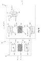
Figure 11 schematically illustrates a diagram of the steps of a process of quantification of the presence or the absence of light and of characterization of light along a first spatial direction, along a second spatial direction and along a third spatial direction, according to an embodiment of the invention. - Some embodiments of apparatus and methods in accordance with embodiments of the present invention are now described, by way of example only, and with reference to the accompanying drawings. The description is to be regarded as illustrative in nature and not as restricted.
-
Figure 1 schematically illustrates astack 1 according to an embodiment of the invention. Thestack 1 comprises: - a first metallic layer M1 extending along a first reference plane P1;
- a dielectric layer D extending along the first metallic layer M1;
- a second metallic layer M2 extending along the dielectric layer D.
- the first metallic layer M1 and the second metallic layer M2 may be made of tantalum Ta, and
- the dielectric layer D may be made of magnesium oxide MgO.
- the first metallic layer M1 and the second metallic layer M2 may be made of Iron Cobalt Boron FeCoB, and
- the dielectric layer D may be made of magnesium oxide MgO.
- The dielectric layer D has a thickness w_D that is measured along a direction perpendicular to the first reference plane P1. Said thickness w_D may typically be comprised between 1 nanometre and 100 nanometres.
Said thickness w_D may beneficially be less than or equal to 4 nanometres, and said thickness w_D may in particular beneficially be comprised between 2 nanometres and 3 nanometres, in order to promote a nominally elastic regime of tunnelling transport. In such a nominally elastic regime of tunnelling transport, electrons may tunnel directly from one interface metallic layer/dielectric layer to another interface metallic layer/dielectric layer. - Alternatively, said thickness w_D may be greater than 4 nanometres. Said thickness w_D may in particular be greater than 10 nanometres. In that case, the transport of electrons across the dielectric layer is interpreted in terms of hopping transport across the dielectric layer D. Within said thickness range indeed, if localized states within the tunnel barrier's band gap arise due to the presence of structural defects, several tunnelling steps will take place as the electron crosses the barrier by hopping onto defect sites.
- The dielectric layer D may for example comprise a material chosen among the followings:
- a magnesium oxide MgO material;
- a strontium titanate SrTiO3 material;
- a tantalum pentoxide Ta2O5 material;
- an aluminium oxide Al2O5 material;
- a titanium dioxide TiO2 material;
- a lanthanum aluminate LaAlO3 material;
- a zirconium oxy-nitride material.
-
Figure 2a schematically illustrates adevice 10 for detecting light according to a first embodiment of the invention, saiddevice 10 having a first geometry. Thedevice 10 having the first geometry is also referred to as "normal dielectric junction". Thedevice 10 comprises: - a substrate S extending along a second reference plane P2;
- a first electrode E1 extending along the substrate S;
- the first metallic layer M1 of the
stack 1 extending along the first electrode E1; - the dielectric layer D of the
stack 1 extending along the metallic layer M1; - the second metallic layer M2 of the
stack 1 extending along the dielectric layer D; - a second electrode E2 extending along the second metallic layer M2 of the
stack 1. - a substrate S made of glass;
- a first electrode E1 comprising a first sub-layer made of tantalum Ta having a thickness of 5 nanometres, a second sub-layer made of cobalt Co having a thickness of 10 nanometres and a third sub-layer made of iridium manganese IrMn having a thickness of 7.5 nanometres;
- a first metallic layer M1 made of FeCoB and having a thickness of about 4 nanometres;
- a dielectric layer D made of MgO and having a thickness of about 2.5 nanometres;
- a second metallic layer M2 made of FeCoB and having a thickness of about 2.5 nanometres;
- a second electrode E2 comprising a first sub-layer made of tantalum Ta having a thickness of 1 nanometre and a second sub-layer made of platinum Pt having a thickness of 1 nanometre.
- Said FeCoB/MgO/FeCoB dielectric junction may nevertheless exhibit sensitivity to the given wavelength ranges outside of the given ranges of parameters, and notably at and beyond room temperature. This table is non-exhaustive in terms of available wavelength ranges. For instance, said FeCoB/MgO/CoFeB dielectric junction may exhibit sensitivity within 375-500 nanometres, with a 10 mV bias voltage and at room temperature.
-
Figure 2b schematically illustrates a device 10' for detecting light according to a second embodiment of the invention, said device 10' having a second geometry. The device 10' having the second geometry is also referred to as "lateral dielectric junction". The device 10' comprises: - the substrate S extending along the second reference plane P2;
- a first electrode E1' extending parallel to a first reference plane P1', the first reference plane P1' being substantially perpendicular to the second reference plane P2, the first electrode E1' being in contact with the substrate S;
- a
stack 1' extending parallel to the first reference plane P1' and comprising:- o a first metallic layer M1' extending along the first electrode E1', the first metallic electrode M1' being in contact with the substrate S;
- o a dielectric layer D' extending along the metallic layer M1', the dielectric layer D' being in contact with the substrate S;
- o a second metallic layer M2' extending along the dielectric layer D', the second metallic layer M2' being in contact with the substrate S;
- a second electrode E2' extending along the second metallic layer M2' of the
stack 1', the second electrode E2' being substantially parallel to the first reference plane P1', the second electrode E2' being in contact with the substrate S. -
Figure 3 schematically illustrates a diagram of the steps of aprocess 100 of detection of light according to an embodiment of the invention. Theprocess 100 comprises the following steps: - a
step 101 of flowing an electric current through thestack 1 of thenormal dielectric junction 10 or through thestack 1' of the lateral dielectric junction 10' that have been previously described, referred to as "first stack"; - a
step 102 of measuring the electric resistance of saidfirst stack - a
step 103 of determining the presence or the absence of light by using the measured electric resistance of saidfirst stack - experimental conditions are controlled so as to insure that no light is impinging said
normal dielectric junction 10 or said lateral dielectric junction 10', and - the electric resistance of the
stack 1 of thenormal dielectric junction 10 or the electric resistance of thestack 1' of the lateral dielectric junction 10' is measured. - The
process 100 that has just been described may further comprise a step of measuring the polarization of light that may be impinging on thestack 1 of thenormal dielectric junction 10 or from thestack 1' of the lateral dielectric junction 10', referred to as "first stack". In the case where light is impinging on saidfirst stack stack 1. In the case where theprocess 100 comprises said step of polarization measurement, theprocess 100 may beneficially comprise a second calibration step, wherein: - experimental conditions are controlled so as to insure that non-polarized light is impinging said
normal dielectric junction 10 or said lateral dielectric junction 10', and - the polarization of light impinging on the
stack 1 of thenormal dielectric junction 10 or of thestack 1' of the lateral dielectric junction 10' is measured. -
Figure 4a schematically illustrates anormal reference device 20 for quantifying detected light that comprises: - the
normal dielectric junction 10 that has been previously described, and - an optically opaque cover Cov extending along the second electrode E2 of the
normal dielectric junction 10, the optically opaque cover Cov being substantially parallel to the second reference plane P2. -
Figure 4b schematically illustrates a lateral reference device 20' for quantifying detected light that comprises: - the lateral dielectric junction 10' that has been previously described, and
- an optically opaque cover Cov' extending along both the first electrode E1', the
stack 1' and the second electrode E2' of the lateral dielectric junction 10', the optically opaque cover Cov' being substantially parallel to the second reference plane P2. -
Figure 4c schematically illustrates adevice 40 allowing quantifying the presence or the absence of light, saiddevice 40 comprising: - a
normal dielectric junction 10, and - a
normal reference device 20 for quantifying detected light. -
Figure 4d schematically illustrates a device 40' allowing quantifying the presence or the absence of light, said device 40' comprising: - a lateral dielectric junction 10', and
- a lateral reference device 20' for quantifying detected light.
-
Figure 4d shows that the lateral dielectric junction 10' and the lateral reference device 20' for quantifying detected light are oriented relative to each other in such a way that the second reference plane P2 of the lateral dielectric junction 10' and the second reference plane P2 of the lateral reference device 20' for quantifying detected light are parallel.
In the particular example of the device 40' illustrated infigure 4d , the first reference plane P2 of the lateral dielectric junction 10' and the first reference plane P2 of the lateral reference device 20' for quantifying detected light are merged, that is to say, the lateral dielectric junction 10' and the lateral reference device 20' for quantifying detected light have the same coordinates according the third axis Z. However it is not necessary, that is to say, the lateral dielectric junction 10' and the lateral reference device 20' for quantifying detected light may have different coordinates according to the third axis Z. The only condition here is that the operational characteristics of both the lateral reference device 20' and the lateral dielectric junction 10' in the absence of light impinging on the lateral dielectric junction 10' be identical. In this case, one may not only position one device at an arbitrary position (x,y) relative to the other, but also beneficially superimpose the lateral dielectric junction 10' on top of the lateral reference device 20' so as to reduce the effective surface area ofdevice 40. - In the particular example of the device 40' illustrated in
figure 4d , the first reference plane P1' of the lateral dielectric junction 10' and the first reference plane P1' of the lateral reference device 20' for quantifying detected light are beneficially parallel. In this way, the device 40' illustrated infigure 4d is adapted both to the case of an isotropic conduction through the dielectric layers D, and to the case of an anisotropic conduction through the dielectric layers D.
If the conduction through the dielectric layers D is isotropic, this means that the conduction will be the same regardless of the absolute direction of current propagation. The lateral reference device 20' for quantifying detected light may have a current C20' that is not parallel to the current C10' of the lateral dielectric junction 10'. In the case of isotropic conduction, the first reference plane P1' of the lateral dielectric junction 10' and the first reference plane P1' of the lateral reference device 20' for quantifying detected light may be parallel but it is not necessary. - If the conduction through the dielectric layers D is anisotropic, then the conduction will not be the same for two given directions of current propagation through D. In this case, to act as a good reference of the current flowing through the lateral dielectric junction 10' in the absence of light, the lateral reference device 20' has a current C20' that is parallel to the current C10' of the lateral dielectric junction 10'. Thus, in the case of anisotropic conduction, the first reference plane P1' of the lateral dielectric junction 10' and the first reference plane P1' of the lateral reference device 20' for quantifying detected light are parallel.
-
Figure 5 schematically illustrates a diagram of the steps of aprocess 200 of quantification of the presence or the absence of light according to an embodiment of the invention. Theprocess 200 typically uses: - a
normal dielectric junction 10 or a lateral dielectric junction 10', referred to as "dielectric junction", and - a
normal reference device 20 for quantifying detected light or a lateral reference device 20' for quantifying detected light, referred to as "reference device for quantifying detected light". - a
step 201 of flowing an electric current:- o through the
stack dielectric junction 10, 10', referred to as "first stack", and - o through the
stack
- o through the
- a
step 202 of measuring the electric resistance of said first stack and of said second stack; - a
step 203 of quantifying the presence or the absence of light around said first stack by comparing the measured electric resistance of said first stack with the measured electric resistance of said second stack. - in the case where a
normal dielectric junction 10 and anormal reference device 20 for quantifying detected light are used, that is, in the case of adevice 40 allowing quantifying the presence or the absence of light: the electric current flowing through said first stack and the electric current flowing through said second stack are both in a same plane; - in the case where a lateral dielectric junction 10' and a lateral reference device 20' for quantifying detected light are used, that is, in the case of a device 40' allowing quantifying the presence or the absence of light: the electric current flowing through said first stack and the electric current flowing through said second stack may be both in a same plane, but it is not necessary.
-
Figure 6a schematically illustrates anormal reference device 30 for characterizing detected light along a first spatial direction that comprises: - the
normal dielectric junction 10 that has been previously described, and - a light depolarizer Dep extending along the second electrode E2 of the
normal dielectric junction 10, the light depolarizer Dep being substantially parallel to the second reference plane P2. - the lateral dielectric junction 10' that has been previously described, and a light depolarizer Dep' extending along both the first electrode E1', the
stack 1' and the second electrode E2' of the lateral dielectric junction 10', the light depolarizer Dep' being substantially parallel to the second reference plane P2. -
Figure 6c schematically illustrates adevice 50 allowing quantifying the presence or the absence of light and characterizing light along a first spatial direction, saiddevice 50 comprising: - a
normal dielectric junction 10, - a
normal reference device 20 for quantifying detected light, and - a
normal reference device 30 for characterizing detected light along a first spatial direction. - the case where the conduction through the dielectric layers D of the
normal dielectric junction 10 and of thenormal reference device 20 for quantifying detected light is isotropic, and - the case where the conduction through the dielectric layers D of the
normal dielectric junction 10 and of thenormal reference device 20 for quantifying detected light is anisotropic. - the case where the impact of depolarized light on conduction is anisotropic, and
- the case where the impact of depolarized light on conduction is isotropic.
- "The impact of depolarized light on conduction is isotropic" means that conduction does not depend on the orientation of the depolarized light that may be impinging on the
normal reference device 30 for characterizing detected light along a first spatial direction. - In the particular example of the
device 50 illustrated infigure 6c , the first reference plane P1 of thenormal dielectric junction 10, the first reference plane P1 of thenormal reference device 20 for quantifying detected light and the first reference plane P1 of thenormal reference device 30 for characterizing detected light along a the first spatial direction are merged, that is to say, thenormal dielectric junction 10, thenormal reference device 20 for quantifying detected light and thenormal reference device 30 for characterizing detected light along a the first spatial direction have the same coordinates according the third axis Z. However it is not necessary, that is to say, thenormal dielectric junction 10, thenormal reference device 20 for quantifying detected light and thenormal reference device 30 for characterizing detected light along a the first spatial direction may have different coordinates according to the third axis Z. Beneficially, thenormal reference device 20 for quantifying detected light and thenormal reference device 30 for characterizing detected light along a the first spatial direction share the same reference plane P1 and are positioned close to one another so that these devices are exposed to the same flux of light.
In the particular example of thedevice 50 illustrated infigure 6c , thenormal dielectric junction 10, thenormal reference device 20 for quantifying detected light and thenormal reference device 30 for characterizing detected light along a the first spatial direction have the same coordinates according to the first axis X, and different coordinates according to the second axis Y.
In another example, thenormal dielectric junction 10, thenormal reference device 20 for quantifying detected light and thenormal reference device 30 for characterizing detected light along a the first spatial direction may have the same coordinates according to the second axis Y, and different coordinates according to the first axis X. - In another example, the
normal dielectric junction 10, thenormal reference device 20 for quantifying detected light and thenormal reference device 30 for characterizing detected light along a the first spatial direction may have different coordinates according the first axis X and different coordinates according to the second axis Y.
While respecting these positioning criteria, the previously described considerations of relative positioning between thenormal dielectric junction 10 and thenormal reference device 20 that apply fordevice 40 also apply to thenormal dielectric junction 10 and thenormal reference device 20 ofdevice 50. -
Figure 6d schematically illustrates a device 50' allowing quantifying the presence or the absence of light and characterizing light along a first spatial direction, said device 50' comprising: - a lateral dielectric junction 10',
- a lateral reference device 20' for quantifying detected light, and
- a lateral reference device 30' for characterizing detected light along a first spatial direction.
- the case where the conduction through the dielectric layers D of the lateral dielectric junction 10' and of the lateral reference device 20' for quantifying detected light is isotropic, and
- the case where the conduction through the dielectric layers D of the lateral dielectric junction 10' and of the lateral reference device 20' for quantifying detected light is anisotropic.
- In the case of isotropic conduction, the first reference plane P1' of the lateral dielectric junction 10' and the first reference plane P1' of the lateral reference device 20' for quantifying detected light may be parallel but it is not necessary.
-
Figure 6d further shows that the lateral dielectric junction 10' and the lateral reference device 30' for characterizing detected light along a first spatial direction are oriented relative to each other in such a way that the second reference plane P2 of the lateral dielectric junction 10' and the second reference plane P2 of the lateral reference device 30' for characterizing detected light along a first spatial direction are parallel. - In the particular example of the device 50' illustrated in
figure 6d , the first reference plane P1' of the lateral dielectric junction 10' and the first reference plane P1' of the lateral reference device 30' for characterizing detected light along a first spatial direction are beneficially parallel. In this way, the device 50' illustrated infigure 6d is both adapted to: - the case where the impact of depolarized light on conduction is anisotropic, and
- the case where the impact of depolarized light on conduction is isotropic.
- While respecting these positioning criteria, the previously described considerations of relative positioning between the lateral dielectric junction 10' and the lateral reference device 20' that apply for device 40' also apply to the lateral dielectric junction 10' and the lateral reference device 20' of device 50'. Beneficially, the lateral reference device 20' for quantifying detected light and the lateral reference device 30' for characterizing detected light along a the first spatial direction share the same reference plane P2 and are positioned close to one another so that these devices are exposed to the same flux of light.
-
Figure 7a schematically illustrates a diagram of the steps of aprocess 300 of characterization of light along a first spatial direction, according to an embodiment of the invention. Theprocess 300 typically uses: - a
normal dielectric junction 10 or a lateral dielectric junction 10', referred to as "dielectric junction", and - a
normal reference device 30 for characterizing detected light along a first spatial direction or a lateral reference device 30' for characterizing detected light along a first spatial direction, referred to as "reference device for characterizing detected light along a first spatial direction". - a
step 301 of flowing an electric current:- o through the stack of the
dielectric junction 10 or 10', referred to as "first stack", and - o through the stack of the reference device for characterizing detected light along a first
spatial direction 30 or 30', referred to as "third stack";
- o through the stack of the
- a
step 302 of measuring the electric resistance of said first stack and of said third stack; - a
step 304 of characterizing the degree to which detected light is polarized along a first spatial direction by comparing the measured electric resistance of said first stack with the measured electric resistance of said third stack. -
Figure 7b schematically illustrates a diagram of the steps of a process 300' of quantification of the presence or the absence of light and of characterization of light along a first spatial direction, according to an embodiment of the invention. The process 300' typically uses: - a
normal dielectric junction 10 or a lateral dielectric junction 10', referred to as "dielectric junction", - a
normal reference device 20 for quantifying detected light or a lateral reference device 20' for quantifying detected light, referred to as "reference device for quantifying detected light", and - a
normal reference device 30 for characterizing detected light along a first spatial direction or a lateral reference device 30' for characterizing detected light along a first spatial direction, referred to as "reference device for characterizing detected light along a first spatial direction". - a step 301' of flowing an electric current:
- o through the stack of the
dielectric junction 10 or 10', referred to as "first stack", - o through the stack of the reference device for quantifying detected light 20 or 20', referred to as "second stack" and
- o through the stack of the reference device for characterizing detected light along a first
spatial direction 30 or 30', referred to as "third stack";
- o through the stack of the
- a step 302' of measuring the electric resistance of said first stack, of said second stack and of said third stack;
- a step 303' of quantifying the presence or the absence of light around said first stack by comparing the measured electric resistance of said first stack with the measured electric resistance of said second stack, and
- a step 304' of characterizing the degree to which light is polarized along a first spatial direction by comparing the measured electric resistance of said first stack with the measured electric resistance of said third stack.
-
Figure 8a schematically illustrates a device 60' allowing quantifying the presence or the absence of light and characterizing light along a first spatial direction and along a second spatial direction.
The device 60' illustrated infigure 8a comprises: - a first lateral dielectric junction 10' that is referenced "10'-1" in
figure 8a and hereinafter for clarity, said first lateral dielectric junction 10'-1 having a first reference plane P1' that is referenced "P1'_10'-1" infigure 8a and hereinafter for clarity, - a lateral reference device 20' for quantifying detected light having a first reference plane P1' that is referenced "P1_20'" in
figure 8a and hereinafter for clarity, - a first lateral reference device 30' for characterizing detected light that is referenced "30'_1" in
figure 8a and hereinafter for clarity, said first lateral reference device 30'_1 having a first reference plane P1' that is referenced "P1_30'-1" infigure 8a and hereinafter for clarity, - a second lateral dielectric junction 10' that is referenced "10_2" in
figure 8a and hereinafter for clarity, said second lateral dielectric junction 10'-2 having a first reference plane P1' that is referenced "P1'_10'-2" infigure 8a and hereinafter for clarity. - the conduction through the dielectric layers D is isotropic, and
- the impact of depolarized light on conduction is isotropic.
-
Figure 8a shows that the first lateral dielectric junction 10'-1 and the lateral reference device 20' for quantifying detected light are oriented relative to each other in such a way that the second reference plane P2 of the first lateral dielectric junction 10'-1 and the second reference plane P2 of the lateral reference device 20' for quantifying detected light are parallel. As previously described in relation withfigure 4d , the first reference plane P1'_10'-1 of the first lateral dielectric junction 10'-1 and the first reference plane P1'_20' of the lateral reference device 20' for quantifying detected light are beneficially parallel, but it is not necessary in the case of isotropic conduction through the dielectric layers D.
Figure 8a further shows that the first lateral dielectric junction 10'-1 and the first lateral reference device 30'-1 for characterizing detected light are oriented relative to each other in such a way that the second reference plane P2 of the first lateral dielectric junction 10'-1 and the second reference plane P2 of the first lateral reference device 30'-1 for characterizing detected light are parallel. As previously described in relation withfigure 6d , the first reference plane P1'_10'-1 of the first lateral dielectric junction 10'-1 and the first reference plane P1_30'-1 of the lateral reference device 30'-1 for characterizing detected light are beneficially parallel, but it is not necessary in the case of isotropic conduction through the dielectric layers D.
The first reference plane P1'_10'-2 of the second lateral dielectric junction 10'-2 is not parallel to the first reference plane P1'_10'-1 of the first lateral dielectric junction 10'-1. In a particular embodiment, the first reference plane P1'_10'-2 of the second lateral dielectric junction 10'-2 is beneficially perpendicular to the first reference plane P1'_10'-1 of the first lateral dielectric junction 10'-1. -
Figure 8b schematically illustrates a device 61' allowing quantifying the presence or the absence of light and characterizing light along a first spatial direction and along a second spatial direction, according to a first variant.
The device 61' according to the first variant illustrated infigure 8b further comprises: - a second lateral reference device 30' for characterizing detected light that is referenced "30'_2" in
figure 8b and hereinafter for clarity, said second lateral reference device 30'_2 having a first reference plane P1' that is referenced "P1'_30'-2" infigure 8b and hereinafter for clarity, - the case where the conduction through the dielectric layers D is isotropic, and
- both the case where the impact of depolarized light on conduction is anisotropic and the case where the impact of depolarized light on conduction is isotropic.
-
Figure 8b shows that the second lateral dielectric junction 10'-2 and the second lateral reference device 30'-2 for characterizing detected light are oriented relative to each other in such a way that the second reference plane P2 of the second lateral dielectric junction 10'-2 and the second reference plane P2 of the second lateral reference device 30'-2 for characterizing detected light are parallel. -
Figure 8b also shows that the second lateral dielectric junction 10'-2 and the second lateral reference device 30'-2 for characterizing detected light are oriented relative to each other in such a way that the first reference plane P1'_10'-2 of the second lateral dielectric junction 10'-2 and the first reference plane P1'_30'-2 of the second lateral reference device 30'-2 are parallel, in order to address the case of anisotropic impact of depolarized light on conduction through the dielectric layer D of the second lateral reference device 30'-2 for characterizing detected light. As previously described in relation withfigure 6d , the first reference plane P1'_10'-1 of the first lateral dielectric junction 10'-1 and the first reference plane P1'_30'-1 of the lateral reference device 30'-1 for characterizing detected light are beneficially parallel, but it is not necessary in the case of isotropic impact of depolarized light on conduction through the dielectric layer D of the second lateral reference device 30'-2 for characterizing detected light. -
Figure 8c schematically illustrates a device 62' allowing quantifying the presence or the absence of light and characterizing light along a first spatial direction and along a second spatial direction, according to a second variant. The device 62' according to the second variant illustrated infigure 8c further comprises: - a second lateral reference device 20' for quantifying detected light that is referenced "20'-2" in
figure 8c and hereinafter for clarity, said second lateral reference device 20'-2 having a first reference plane P1' that is referenced "P1 _20'-2"" infigure 8c and hereinafter for clarity. - both the case where the conduction through the dielectric layers D is isotropic and the case where the conduction through the dielectric layers D is anisotropic, and
- both the case where the impact of depolarized light on conduction is anisotropic and the case where the impact of depolarized light on conduction is isotropic.
-
Figure 8c shows that the second lateral dielectric junction 10'-2 and the second lateral reference device 20'-2 for quantifying detected light are oriented relative to each other in such a way that the second reference plane P2 of the second lateral dielectric junction 10'-2 and the second reference plane P2 of the second lateral reference device 20'-2 for quantifying detected light are parallel.
Figure 8c also shows that the second lateral dielectric junction 10'-2 and the second lateral reference device 20'-2 for quantifying detected light are oriented relative to each other in such a way that the first reference plane P1'_10'-2 of the second lateral dielectric junction 10'-2 and the first reference plane P1'_20'-2 of the second lateral reference device 20'-2 are parallel, in order to address the case of anisotropic conduction through the dielectric layers D. - Three particular examples of devices allowing quantifying the presence or the absence of light and characterizing light along a first spatial direction and along a second spatial direction, according to the invention, have just been described:
- the device 60' illustrated in
figure 8a ; - the device 61' according to the first variant illustrated in
figure 8b , and - the device 62' according to the second variant illustrated in
figure 8c . -
Figure 9 schematically illustrates a diagram of the steps of aprocess 400 of quantification of the presence or the absence of light and of characterization of light along a first spatial direction and along a second spatial direction, according to an embodiment of the invention. Theprocess 400 may typically use the device 60' illustrated infigure 8a or the device 61' illustrated infigure 8b or the device 62' illustrated infigure 8c .
Theprocess 400 thus typically uses: - a first
normal dielectric junction 10 or a first lateral dielectric junction 10', referred to as "first dielectric junction", - at least a
normal reference device 20 for quantifying detected light or a lateral reference device 20' for quantifying detected light, referred to as "reference device for quantifying detected light", - at least a
normal reference device 30 for characterizing detected light or a lateral reference device 30' for characterizing detected light, referred to as "reference device for characterizing detected light", and - a second
normal dielectric junction 10 or a second lateral dielectric junction 10', referred to as "second dielectric junction". - a
step 401 of flowing an electric current:- o through the stack of the first dielectric junction,
- o through the stack of the reference device for quantifying detected light,
- o through the stack of the reference device for characterizing detected light, and
- o through the stack of the second dielectric junction;
- a
step 402 of measuring the electric resistance of:- o the first dielectric junction,
- o the reference device for quantifying detected light,
- o the reference device for characterizing detected light, and
- o the second dielectric junction;
- a
step 403 of quantifying the presence or the absence of light:- o around the first dielectric junction by comparing the measured electric resistance of the first dielectric junction with the measured electric resistance of the reference device for quantifying detected light,
- o and/or around the second dielectric junction by comparing the measured electric resistance of the second dielectric junction with the measured electric resistance of the reference device for quantifying detected light;
- a
step 404 of characterizing the degree to which light around the first dielectric junction is polarized along a first spatial direction by comparing the measured electric resistance of the first dielectric junction with the measured electric resistance of the reference device for characterizing detected light; - a
step 405 of characterizing the degree to which light around the second dielectric junction is polarized along a second spatial direction by comparing the measured electric resistance of the second dielectric junction with the measured electric resistance of the reference device for characterizing detected light. -
Figure 10 schematically illustrates adevice 70 allowing quantifying the presence or the absence of light and characterizing light along a first spatial direction, along a second spatial direction and along a third spatial direction.
Thedevice 70 illustrated infigure 10 comprises: - the
device 50 previously described in relation withfigure 6c , and - the device 60' previously described in relation with
figure 8a . - Other examples of devices according to the invention allowing quantifying the presence or the absence of light and characterizing light along a first spatial direction, along a second spatial direction and along a third spatial direction are possible within the scope of the present invention, and especially:
- a device comprising the
device 50 previously described in relation withfigure 6c and the device 61' previously described in relation withfigure 8b ; - a device comprising the
device 50 previously described in relation withfigure 6c and the device 62' previously described in relation withfigure 8c . - the lateral dielectric junction 10'-1, referred to as "first dielectric junction";
- the lateral dielectric junction 10'-2, referred to as "second dielectric junction";
- the normal dielectric junction 10-3, referred to as "third dielectric junction";
- the lateral reference device 20' for quantifying detected light;
- the
normal reference device 20 for quantifying detected light; - the lateral reference device 30'-1 for characterizing detected light, and
- the
normal reference device 30 for characterizing detected light. - a
step 501 of flowing an electric current:- o through the stack of the first dielectric junction 10'-1,
- o through the stack of the second dielectric junction 10'-2,
- o through the stack of the third dielectric junction 10-3,
- o through the stack of the lateral reference device 20' for quantifying detected light,
- o through the stack of the
normal reference device 20 for quantifying detected light, - o through the stack of the lateral reference device 30' for characterizing detected light, and
- o through the stack of the
normal reference device 30 for characterizing detected light;
- a
step 502 of measuring the electric resistance of:- o the first dielectric junction 10'-1,
- o the second dielectric junction 10'-2,
- o the third dielectric junction 10-3,
- o the lateral reference device 20' for quantifying detected light,
- o the
normal reference device 20 for quantifying detected light, - o the lateral reference device 30' for characterizing detected light, and
- o the
normal reference device 30 for characterizing detected light;
- a
step 503 of quantifying the presence or the absence of light:- o around the first dielectric junction 10'-1 by comparing the measured electric resistance of the first dielectric junction 10'-1 with the measured electric resistance of the lateral reference device 20' for quantifying detected light,
- o and/or around the second dielectric 10'-2 junction by comparing the measured electric resistance of the second dielectric junction 10'-2 with the measured electric resistance of the lateral reference device 20' for quantifying detected light, and
- o and/or around the third dielectric junction 10-3 by comparing the measured electric resistance of the third dielectric junction 10-3 with the measured electric resistance of the
normal reference device 20 for quantifying detected light;
- a
step 504 of characterizing the degree to which light around the first dielectric junction 10'-1 is polarized along a first spatial direction by comparing the measured electric resistance of the first dielectric junction 10'-1 with the measured electric resistance of the lateral reference device 30'-1 for characterizing detected light; - a
step 505 of characterizing the degree to which light around the second dielectric junction 10'-2 is polarized along a second spatial direction by comparing the measured electric resistance of the second dielectric junction 10'-2 with the measured electric resistance of the lateral reference device 30'-1 for characterizing detected light; - a
step 506 of characterizing the degree to which light around the third dielectric junction 10-3 is polarized along a third spatial direction by comparing the measured electric resistance of the third dielectric junction 10-3 with the measured electric resistance of thenormal reference device 30 for characterizing detected light. - A three-dimensional polarization vector of light, that is to say a three-dimensional vector comprising the degree to which light impinging on the device is polarized along the first, second and third spatial directions, may thus be obtained, allowing one to determine the propagation direction of light.
In a particular embodiment of the invention, the first metallic layer M1 may be a first magnetic layer, the second metallic layer M2 may be a second magnetic layer and the dielectric layer D may be a non-magnetic layer ensuring the magnetic decoupling of the first and second magnetic layers.
In a first particular example:
A
| Bias voltage (V) | Temperature (K) | Wavelength (nm) |
| ± 1.2 | 30-80 | 375-500 |
| ± 0.8 | 80-250 | 575-725 |
In other words, in the lateral dielectric junction 10', current that flows through the

The Al film of the opaque cover Cov' is deposited on the Lif film. The Al film may have a thickness of 65 nm, as previously described.
In the case a current flows through the
In the particular example of the
In another example, the
In another example, the
In the particular example of the
In the particular example of the device 40' illustrated in
In another example, the lateral dielectric junction 10' and the lateral reference device 20' for quantifying detected light may have the same coordinates according to the second axis Y, and different coordinates according to the first axis X.
In another example, the lateral dielectric junction 10' and the lateral reference device 20' for quantifying detected light may have different coordinates according the first axis X and different coordinates according to the second axis Y.
It is to be noted that:
In the particular example of the device 50' illustrated in
The
Claims (13)
- A process (100, 200, 300, 300', 400, 500) of detection of light comprising:- a step (101, 201, 301, 301', 401, 501) of flowing an electric current through at least a first dielectric junction (10, 10', 10'-1), said first dielectric junction comprising at least a first metallic layer (M1) extending along a first reference plane (P1, P1') and a second metallic layer (M2) extending parallel to said first reference plane (P1, P1'), said first and second metallic layers being separated from each other by a dielectric layer (D) ensuring non-ohmic conduction between said first and second metallic layers;- a step (102, 202, 302, 302', 402, 502) of measuring the electric resistance of the first dielectric junction (10, 10', 10'-1);- a step (103, 203, 303' 403, 503) of determining the presence or the absence of light by using the measured electric resistance of the first dielectric junction (10, 10', 10'-1).
- A process (100, 200, 300, 300', 400, 500) according to claim 1 wherein said dielectric layer (D) has a thickness (w_D) between 0.5 nm and 100 nm, said thickness being measured along a direction perpendicular to the first reference plane (P1, P1').
- A process (100, 200, 300, 300', 400, 500) according to claim 1 or 2 wherein said dielectric layer (D) has a thickness (w_D) that is less than or equal to 4 nm, said thickness (w_D) being measured along a direction perpendicular to the first reference plane (P1, P1').
- A process (100, 200, 300, 300', 400, 500) according to claim 3 wherein said thickness (w_D) of said dielectric layer (D) is between 0.6 and 3 nm.
- A process (100, 200, 300, 300', 400, 500) according to any of the previous claims, wherein the dielectric junction (10) comprises:- a substrate (S) extending along a second reference plane (P2), the second reference plane (P2) being substantially parallel to the first reference plane (P1);- a first electrode (E1) extending along the substrate (S);- the first metallic layer (M1) extending along the first electrode (E1);- the dielectric layer (D) extending along the first metallic layer (M1);- the second metallic layer (M2) extending along the dielectric layer (D);- a second electrode (E2) extending along the second metallic layer (M2).
- A process (100, 200, 300, 300', 400, 500) according to any of the claims 1 to 5, wherein the first dielectric junction (10', 10'-1) comprises:- a substrate (S) extending along a second reference plane (P2), the second reference plane (P2) being substantially perpendicular to the first reference plane (P1');- a first electrode (E1') extending along a plane that is substantially perpendicular to the second reference plane (P2) and substantially parallel to the first reference plane (P1'),- the first metallic layer (M1) extending along the first electrode (E1'),- the dielectric layer (D) extending along the first metallic layer (M1),- the second metallic layer (M2) extending along the dielectric layer (D),- a second electrode (E2') extending along the second metallic layer (M2).
- A process (100, 200, 300, 300', 400, 500) according to any of the previous claims wherein said dielectric layer (D) is made of magnesium oxide MgO.
- A process (200, 300', 400, 500) according to any of the previous claims wherein a plurality of dielectric junctions is used, said plurality of dielectric junctions comprising at least the first dielectric junction (10, 10', 10'-1) and a reference device for quantifying detected light (20, 20') further comprising an optically opaque cover (Cov, Cov'),
the process further comprising:- a step (201, 301', 401, 501) of flowing an electric current through said first dielectric junction (10, 10', 10'-1) and through said reference device for quantifying detected light (20, 20');- a step (202, 302', 402, 502) of measuring the electric resistance of said first dielectric junction (10, 10', 10'-1) and of said reference device for quantifying detected light (20, 20');- a step (203, 303', 403, 503) of quantifying the presence or the absence of light around said first dielectric junction (10, 10', 10'-1) by comparing the measured electric resistance of the first dielectric junction with the measured electric resistance of the reference device for quantifying detected light. - A process (300, 300', 400, 500) according to any of claims 1 to 7 wherein a plurality of dielectric junctions is used, said plurality of dielectric junctions comprising at least the first dielectric junction (10, 10', 10'-1) and a reference device for characterizing detected light (30, 30', 30'-1) further comprising a light depolarizer (Dep, Dep'),
the process comprising:- a step (301, 301', 401, 501) of flowing an electric current through said first dielectric junction (10, 10', 10'-1) and through said third reference device for characterizing detected light (30, 30', 30'-1);- a step (302, 302', 402, 502) of measuring the electric resistance of said first dielectric junction (10, 10', 10'-1) and of said reference device for characterizing detected light (30, 30', 30'-1);- a step (304, 304', 404, 504) of comparing the measured electric resistance of the first electric junction with the measured electric resistance of the reference device for characterizing detected light, in order to characterize the degree to which light around the first dielectric junction is polarized along a first spatial direction. - A process (300', 400, 500) according to claim 9 wherein the plurality of dielectric junctions further comprises a reference device for quantifying detected light (20, 20') comprising an optically opaque cover (Cov, Cov'), the process comprising:- a step (301', 401, 501) of flowing an electric current through said first dielectric junction (10, 10', 10'-1), through said reference device for quantifying detected light (20, 20') and through said reference device for characterizing detected light (30, 30', 30'-1);- a step (302', 402, 502) of measuring the electric resistance of the first dielectric junction (10, 10', 10'-1), of the reference device for quantifying detected light (20, 20') and of the reference device for characterizing detected light (30, 30', 30'-1);- a step (303', 403, 503) of comparing the measured electric resistance of the first dielectric junction (10, 10', 10'-1) with the measured electric resistance of the reference device for quantifying detected light (20, 20') in order to quantify the presence or the absence of light around the first dielectric junction (10, 10', 10'-1), and- a step (304', 404, 504) of comparing the measured electric resistance of the first dielectric junction (10, 10', 10'-1) with the measured electric resistance of the reference device for characterizing detected light (30, 30', 30'-1) in order to characterize the degree to which light around the first dielectric junction (10, 10', 10'-1) is polarized along a first spatial direction.
- A process (400, 500) according to claim 10 wherein the plurality of dielectric junctions further comprises a second dielectric junction (10'-2), the process comprising:- a step (401, 501) of flowing an electric current at least through the first dielectric junction (10'-1), through the second dielectric junction (10'-2), through the reference device for quantifying detected light (20') and through the reference device for characterizing detected light (30'-1);- a step (402, 502) of measuring the electric resistance of the first dielectric junction (10'-1), of the second dielectric junction (10'-2), of the reference device for quantifying detected light (20') and of the reference device for characterizing detected light (30'-1);- a step (403, 503) of comparing the measured electric resistance of the first dielectric junction (10'-1) with the measured electric resistance of the reference device for quantifying detected light (20') in order to quantify the presence or the absence of light around the first dielectric junction (10'-1), and/or of comparing the measured electric resistance of the second dielectric junction (10'-2) with the measured electric resistance of the reference device for quantifying detected light (20') in order to quantify the presence or the absence of light around the second dielectric junction (10'-2);- a step (404, 504) of comparing the measured electric resistance of the first dielectric junction (10'-1) with the measured electric resistance of the reference device for characterizing detected light (30'-1) in order to characterize the degree to which light around the first dielectric junction (10'-1) is polarized along a first spatial direction;- a step (405, 505) of comparing the measured electric resistance of the second dielectric junction (10'-2) with the measured electric resistance of the reference device for characterizing detected light (30'-1) in order to characterize the degree to which light around the second dielectric junction (10'-2) is polarized along a second spatial direction.
- A process (500) according to claim 11 wherein the plurality of dielectric junctions further comprises a third dielectric junction (10-3), a second reference device for quantifying detected light (20) and a second reference device for characterizing detected light (30), the process comprising:- a step (501) of flowing an electric current at least through the first dielectric junction (10'-1), through the second dielectric junction (10'-2), through the third dielectric junction (10-3), through the reference device for quantifying detected light (20'), through the second reference device for quantifying detected light (20), through the reference device for characterizing detected light (30'-1) and through the second reference device for characterizing detected light (30);- a step (502) of measuring the electric resistance of the first dielectric junction (10'-1), of the second dielectric junction (10'-2), of the third dielectric junction (10-3), of the reference device for quantifying detected light (20'), of the second reference device for quantifying detected light (20), of the reference device for characterizing detected light (30'-1) and of the second reference device for characterizing detected light (30);- a step (503) of comparing the measured electric resistance of the first dielectric junction (10'-1) with the measured electric resistance of the reference device for quantifying detected light (20') in order to quantify the presence or the absence of light around the first dielectric junction (10'-1), and/or of comparing the measured electric resistance of the second dielectric junction (10'-2) with the measured electric resistance of the reference device for quantifying detected light (20') in order to quantify the presence or the absence of light around the second dielectric junction (10'-2), and/or of comparing the measured electric resistance of the third dielectric junction (10-3) with the measured electric resistance of the second reference device for quantifying detected light (20) in order to quantify the presence or the absence of light around the third dielectric junction (10-3);- a step (504) of comparing the measured electric resistance of the first dielectric junction (10'-1) with the measured electric resistance of the reference device for characterizing detected light (30'-1) in order to characterize the degree to which light around the first dielectric junction (10'-1) is polarized along a first spatial direction;- a step (505) of comparing the measured electric resistance of the second dielectric junction (10'-2) with the measured electric resistance of the reference device for characterizing detected light (30'-1) in order to characterize the degree to which light around the second dielectric junction (10'-2) is polarized along a second spatial direction;- a step (506) of comparing the measured electric resistance of the third dielectric junction (10-3) with the measured electric resistance of the second reference device for characterizing detected light (30) in order to characterize the degree to which light around the third dielectric junction (10-3) is polarized along a third spatial direction.
- A process (500) according to the previous claim wherein a three-dimensional polarization vector of light is obtained, the process comprising a step of determining the propagation direction of light.
Priority Applications (2)
| Application Number | Priority Date | Filing Date | Title |
|---|---|---|---|
| EP14180354.4A EP2982950A1 (en) | 2014-08-08 | 2014-08-08 | Process of detection of light and associated device |
| PCT/EP2015/067406 WO2016020243A1 (en) | 2014-08-08 | 2015-07-29 | Process of detection of light and associated device |
Applications Claiming Priority (1)
| Application Number | Priority Date | Filing Date | Title |
|---|---|---|---|
| EP14180354.4A EP2982950A1 (en) | 2014-08-08 | 2014-08-08 | Process of detection of light and associated device |
Publications (1)
| Publication Number | Publication Date |
|---|---|
| EP2982950A1 true EP2982950A1 (en) | 2016-02-10 |
Family
ID=51454531
Family Applications (1)
| Application Number | Title | Priority Date | Filing Date |
|---|---|---|---|
| EP14180354.4A Withdrawn EP2982950A1 (en) | 2014-08-08 | 2014-08-08 | Process of detection of light and associated device |
Country Status (2)
| Country | Link |
|---|---|
| EP (1) | EP2982950A1 (en) |
| WO (1) | WO2016020243A1 (en) |
Citations (5)
| Publication number | Priority date | Publication date | Assignee | Title |
|---|---|---|---|---|
| JP2005011907A (en) * | 2003-06-17 | 2005-01-13 | Japan Science & Technology Agency | Spin-injection magnetization reversal magnetoresistive element using quantum size effect |
| EP2190022A1 (en) * | 2008-11-20 | 2010-05-26 | Hitachi Ltd. | Spin-polarised charge carrier device |
| US20110001473A1 (en) * | 2008-02-13 | 2011-01-06 | University Of Delaware | Electromagnetic wave detection methods and apparatus |
| US20110026296A1 (en) * | 2009-07-30 | 2011-02-03 | National Institute Of Advanced Industrial Science And Technology | Nonvolatile Optical Memory Element, Memory Device, and Reading Method Thereof |
| EP2680321A2 (en) * | 2007-12-18 | 2014-01-01 | Marek T. Michalewicz | Quantum tunneling photodetector array |
-
2014
- 2014-08-08 EP EP14180354.4A patent/EP2982950A1/en not_active Withdrawn
-
2015
- 2015-07-29 WO PCT/EP2015/067406 patent/WO2016020243A1/en not_active Ceased
Patent Citations (5)
| Publication number | Priority date | Publication date | Assignee | Title |
|---|---|---|---|---|
| JP2005011907A (en) * | 2003-06-17 | 2005-01-13 | Japan Science & Technology Agency | Spin-injection magnetization reversal magnetoresistive element using quantum size effect |
| EP2680321A2 (en) * | 2007-12-18 | 2014-01-01 | Marek T. Michalewicz | Quantum tunneling photodetector array |
| US20110001473A1 (en) * | 2008-02-13 | 2011-01-06 | University Of Delaware | Electromagnetic wave detection methods and apparatus |
| EP2190022A1 (en) * | 2008-11-20 | 2010-05-26 | Hitachi Ltd. | Spin-polarised charge carrier device |
| US20110026296A1 (en) * | 2009-07-30 | 2011-02-03 | National Institute Of Advanced Industrial Science And Technology | Nonvolatile Optical Memory Element, Memory Device, and Reading Method Thereof |
Non-Patent Citations (2)
| Title |
|---|
| HÖVEL S ET AL: "Electrical detection of photoinduced spins both at room temperature and in remanence", APPLIED PHYSICS LETTERS, AMERICAN INSTITUTE OF PHYSICS, US, vol. 92, no. 24, 17 June 2008 (2008-06-17), pages 242102 - 242102, XP012107568, ISSN: 0003-6951, DOI: 10.1063/1.2948856 * |
| RINALDI C ET AL: "Epitaxial Fe/MgO/Ge spin-photodiodes for integrated detection of light helicity at room temperature", JOURNAL OF APPLIED PHYSICS, AMERICAN INSTITUTE OF PHYSICS, US, vol. 111, no. 7, 6 March 2012 (2012-03-06), pages 7C312 - 7C312, XP012159120, ISSN: 0021-8979, [retrieved on 20120306], DOI: 10.1063/1.3676243 * |
Also Published As
| Publication number | Publication date |
|---|---|
| WO2016020243A1 (en) | 2016-02-11 |
Similar Documents
| Publication | Publication Date | Title |
|---|---|---|
| US10823683B1 (en) | Method for detecting defects in deep features with laser enhanced electron tunneling effect | |
| US10515999B2 (en) | Imaging element, image sensor, imaging apparatus, and information processing apparatus | |
| US9860466B2 (en) | Sensor with electrically controllable aperture for inspection and metrology systems | |
| Sánchez-Santolino et al. | Probing the internal atomic charge density distributions in real space | |
| JP6668176B2 (en) | Sensor | |
| US10152998B2 (en) | Features maps of articles with polarized light | |
| US20130293871A1 (en) | Sensor for spectral-polarization imaging | |
| US10438365B2 (en) | Imaging device, subject information acquisition method, and computer program | |
| Detemple et al. | Ruddlesden-Popper faults in LaNiO3/LaAlO3 superlattices | |
| US10147824B2 (en) | Detector comprising a variable capacitance diode | |
| Matveyev et al. | Polarization-dependent electric potential distribution across nanoscale ferroelectric Hf 0.5 Zr 0.5 O 2 in functional memory capacitors | |
| US20150077750A1 (en) | Ellipsometer for detecting surface | |
| EP2982950A1 (en) | Process of detection of light and associated device | |
| US11237121B2 (en) | Electron microscope, and method for observing measurement sample | |
| JP7682737B2 (en) | Inspection system and method for secondary battery | |
| US20150276493A1 (en) | Thermoelectric conversion element, light detection device, electronic apparatus | |
| CN113030016B (en) | Weak measurement-based method for identifying type of Wilson semimetal and measuring inclination of Wilson cone | |
| US9800805B2 (en) | Frequency selective imaging system | |
| An | Application of imaging ellipsometry to the detection of latent fingermarks | |
| Jian et al. | Monitoring metal contamination of silicon by multiwavelength room temperature photoluminescence spectroscopy | |
| JP2018082022A (en) | PHOTOELECTRIC CONVERSION ELEMENT, SOLID-STATE IMAGING ELEMENT, AND ELECTRONIC DEVICE | |
| JP7154531B2 (en) | Electronic device evaluation method and evaluation apparatus | |
| Olsen et al. | Initial results and field applications of a polarization imaging camera | |
| US11692928B2 (en) | Particle analysis using light microscope and multi-pixel polarization filter | |
| JP4909154B2 (en) | Method and apparatus for measuring pole figure of crystal grains |
Legal Events
| Date | Code | Title | Description |
|---|---|---|---|
| PUAI | Public reference made under article 153(3) epc to a published international application that has entered the european phase |
Free format text: ORIGINAL CODE: 0009012 |
|
| AK | Designated contracting states |
Kind code of ref document: A1 Designated state(s): AL AT BE BG CH CY CZ DE DK EE ES FI FR GB GR HR HU IE IS IT LI LT LU LV MC MK MT NL NO PL PT RO RS SE SI SK SM TR |
|
| AX | Request for extension of the european patent |
Extension state: BA ME |
|
| STAA | Information on the status of an ep patent application or granted ep patent |
Free format text: STATUS: THE APPLICATION IS DEEMED TO BE WITHDRAWN |
|
| 18D | Application deemed to be withdrawn |
Effective date: 20160811 |