EP2980988A1 - Envelope tracking with low frequency loss correction - Google Patents
Envelope tracking with low frequency loss correction Download PDFInfo
- Publication number
- EP2980988A1 EP2980988A1 EP15178690.2A EP15178690A EP2980988A1 EP 2980988 A1 EP2980988 A1 EP 2980988A1 EP 15178690 A EP15178690 A EP 15178690A EP 2980988 A1 EP2980988 A1 EP 2980988A1
- Authority
- EP
- European Patent Office
- Prior art keywords
- signal
- low frequency
- voltage supply
- power amplifier
- error
- Prior art date
- Legal status (The legal status is an assumption and is not a legal conclusion. Google has not performed a legal analysis and makes no representation as to the accuracy of the status listed.)
- Granted
Links
Images





Classifications
-
- H—ELECTRICITY
- H03—ELECTRONIC CIRCUITRY
- H03F—AMPLIFIERS
- H03F1/00—Details of amplifiers with only discharge tubes, only semiconductor devices or only unspecified devices as amplifying elements
- H03F1/02—Modifications of amplifiers to raise the efficiency, e.g. gliding Class A stages, use of an auxiliary oscillation
- H03F1/0205—Modifications of amplifiers to raise the efficiency, e.g. gliding Class A stages, use of an auxiliary oscillation in transistor amplifiers
- H03F1/0211—Modifications of amplifiers to raise the efficiency, e.g. gliding Class A stages, use of an auxiliary oscillation in transistor amplifiers with control of the supply voltage or current
- H03F1/0216—Continuous control
-
- H—ELECTRICITY
- H02—GENERATION; CONVERSION OR DISTRIBUTION OF ELECTRIC POWER
- H02M—APPARATUS FOR CONVERSION BETWEEN AC AND AC, BETWEEN AC AND DC, OR BETWEEN DC AND DC, AND FOR USE WITH MAINS OR SIMILAR POWER SUPPLY SYSTEMS; CONVERSION OF DC OR AC INPUT POWER INTO SURGE OUTPUT POWER; CONTROL OR REGULATION THEREOF
- H02M3/00—Conversion of DC power input into DC power output
- H02M3/02—Conversion of DC power input into DC power output without intermediate conversion into AC
- H02M3/04—Conversion of DC power input into DC power output without intermediate conversion into AC by static converters
- H02M3/10—Conversion of DC power input into DC power output without intermediate conversion into AC by static converters using discharge tubes with control electrode or semiconductor devices with control electrode
- H02M3/145—Conversion of DC power input into DC power output without intermediate conversion into AC by static converters using discharge tubes with control electrode or semiconductor devices with control electrode using devices of a triode or transistor type requiring continuous application of a control signal
- H02M3/155—Conversion of DC power input into DC power output without intermediate conversion into AC by static converters using discharge tubes with control electrode or semiconductor devices with control electrode using devices of a triode or transistor type requiring continuous application of a control signal using semiconductor devices only
-
- H—ELECTRICITY
- H03—ELECTRONIC CIRCUITRY
- H03F—AMPLIFIERS
- H03F1/00—Details of amplifiers with only discharge tubes, only semiconductor devices or only unspecified devices as amplifying elements
- H03F1/02—Modifications of amplifiers to raise the efficiency, e.g. gliding Class A stages, use of an auxiliary oscillation
- H03F1/0205—Modifications of amplifiers to raise the efficiency, e.g. gliding Class A stages, use of an auxiliary oscillation in transistor amplifiers
- H03F1/0211—Modifications of amplifiers to raise the efficiency, e.g. gliding Class A stages, use of an auxiliary oscillation in transistor amplifiers with control of the supply voltage or current
- H03F1/0216—Continuous control
- H03F1/0222—Continuous control by using a signal derived from the input signal
-
- H—ELECTRICITY
- H03—ELECTRONIC CIRCUITRY
- H03F—AMPLIFIERS
- H03F1/00—Details of amplifiers with only discharge tubes, only semiconductor devices or only unspecified devices as amplifying elements
- H03F1/02—Modifications of amplifiers to raise the efficiency, e.g. gliding Class A stages, use of an auxiliary oscillation
- H03F1/0205—Modifications of amplifiers to raise the efficiency, e.g. gliding Class A stages, use of an auxiliary oscillation in transistor amplifiers
- H03F1/0211—Modifications of amplifiers to raise the efficiency, e.g. gliding Class A stages, use of an auxiliary oscillation in transistor amplifiers with control of the supply voltage or current
- H03F1/0216—Continuous control
- H03F1/0222—Continuous control by using a signal derived from the input signal
- H03F1/0227—Continuous control by using a signal derived from the input signal using supply converters
-
- H—ELECTRICITY
- H03—ELECTRONIC CIRCUITRY
- H03F—AMPLIFIERS
- H03F1/00—Details of amplifiers with only discharge tubes, only semiconductor devices or only unspecified devices as amplifying elements
- H03F1/02—Modifications of amplifiers to raise the efficiency, e.g. gliding Class A stages, use of an auxiliary oscillation
- H03F1/0205—Modifications of amplifiers to raise the efficiency, e.g. gliding Class A stages, use of an auxiliary oscillation in transistor amplifiers
- H03F1/0211—Modifications of amplifiers to raise the efficiency, e.g. gliding Class A stages, use of an auxiliary oscillation in transistor amplifiers with control of the supply voltage or current
- H03F1/0244—Stepped control
- H03F1/025—Stepped control by using a signal derived from the input signal
-
- H—ELECTRICITY
- H03—ELECTRONIC CIRCUITRY
- H03F—AMPLIFIERS
- H03F1/00—Details of amplifiers with only discharge tubes, only semiconductor devices or only unspecified devices as amplifying elements
- H03F1/02—Modifications of amplifiers to raise the efficiency, e.g. gliding Class A stages, use of an auxiliary oscillation
- H03F1/0205—Modifications of amplifiers to raise the efficiency, e.g. gliding Class A stages, use of an auxiliary oscillation in transistor amplifiers
- H03F1/0211—Modifications of amplifiers to raise the efficiency, e.g. gliding Class A stages, use of an auxiliary oscillation in transistor amplifiers with control of the supply voltage or current
- H03F1/0244—Stepped control
- H03F1/0255—Stepped control by using a signal derived from the output signal
-
- H—ELECTRICITY
- H03—ELECTRONIC CIRCUITRY
- H03F—AMPLIFIERS
- H03F1/00—Details of amplifiers with only discharge tubes, only semiconductor devices or only unspecified devices as amplifying elements
- H03F1/02—Modifications of amplifiers to raise the efficiency, e.g. gliding Class A stages, use of an auxiliary oscillation
- H03F1/0205—Modifications of amplifiers to raise the efficiency, e.g. gliding Class A stages, use of an auxiliary oscillation in transistor amplifiers
- H03F1/0277—Selecting one or more amplifiers from a plurality of amplifiers
-
- H—ELECTRICITY
- H03—ELECTRONIC CIRCUITRY
- H03F—AMPLIFIERS
- H03F3/00—Amplifiers with only discharge tubes or only semiconductor devices as amplifying elements
- H03F3/04—Amplifiers with only discharge tubes or only semiconductor devices as amplifying elements with semiconductor devices only
- H03F3/08—Amplifiers with only discharge tubes or only semiconductor devices as amplifying elements with semiconductor devices only controlled by light
- H03F3/082—Amplifiers with only discharge tubes or only semiconductor devices as amplifying elements with semiconductor devices only controlled by light with FET's
-
- H—ELECTRICITY
- H03—ELECTRONIC CIRCUITRY
- H03F—AMPLIFIERS
- H03F3/00—Amplifiers with only discharge tubes or only semiconductor devices as amplifying elements
- H03F3/189—High-frequency amplifiers, e.g. radio frequency amplifiers
- H03F3/19—High-frequency amplifiers, e.g. radio frequency amplifiers with semiconductor devices only
- H03F3/195—High-frequency amplifiers, e.g. radio frequency amplifiers with semiconductor devices only in integrated circuits
-
- H—ELECTRICITY
- H03—ELECTRONIC CIRCUITRY
- H03F—AMPLIFIERS
- H03F3/00—Amplifiers with only discharge tubes or only semiconductor devices as amplifying elements
- H03F3/20—Power amplifiers, e.g. Class B amplifiers, Class C amplifiers
- H03F3/24—Power amplifiers, e.g. Class B amplifiers, Class C amplifiers of transmitter output stages
- H03F3/245—Power amplifiers, e.g. Class B amplifiers, Class C amplifiers of transmitter output stages with semiconductor devices only
-
- H—ELECTRICITY
- H03—ELECTRONIC CIRCUITRY
- H03F—AMPLIFIERS
- H03F3/00—Amplifiers with only discharge tubes or only semiconductor devices as amplifying elements
- H03F3/45—Differential amplifiers
- H03F3/45071—Differential amplifiers with semiconductor devices only
-
- H—ELECTRICITY
- H03—ELECTRONIC CIRCUITRY
- H03F—AMPLIFIERS
- H03F3/00—Amplifiers with only discharge tubes or only semiconductor devices as amplifying elements
- H03F3/68—Combinations of amplifiers, e.g. multi-channel amplifiers for stereophonics
-
- H—ELECTRICITY
- H03—ELECTRONIC CIRCUITRY
- H03F—AMPLIFIERS
- H03F3/00—Amplifiers with only discharge tubes or only semiconductor devices as amplifying elements
- H03F3/72—Gated amplifiers, i.e. amplifiers which are rendered operative or inoperative by means of a control signal
-
- H—ELECTRICITY
- H02—GENERATION; CONVERSION OR DISTRIBUTION OF ELECTRIC POWER
- H02M—APPARATUS FOR CONVERSION BETWEEN AC AND AC, BETWEEN AC AND DC, OR BETWEEN DC AND DC, AND FOR USE WITH MAINS OR SIMILAR POWER SUPPLY SYSTEMS; CONVERSION OF DC OR AC INPUT POWER INTO SURGE OUTPUT POWER; CONTROL OR REGULATION THEREOF
- H02M1/00—Details of apparatus for conversion
- H02M1/0045—Converters combining the concepts of switch-mode regulation and linear regulation, e.g. linear pre-regulator to switching converter, linear and switching converter in parallel, same converter or same transistor operating either in linear or switching mode
-
- H—ELECTRICITY
- H03—ELECTRONIC CIRCUITRY
- H03F—AMPLIFIERS
- H03F2200/00—Indexing scheme relating to amplifiers
- H03F2200/102—A non-specified detector of a signal envelope being used in an amplifying circuit
-
- H—ELECTRICITY
- H03—ELECTRONIC CIRCUITRY
- H03F—AMPLIFIERS
- H03F2200/00—Indexing scheme relating to amplifiers
- H03F2200/111—Indexing scheme relating to amplifiers the amplifier being a dual or triple band amplifier, e.g. 900 and 1800 MHz, e.g. switched or not switched, simultaneously or not
-
- H—ELECTRICITY
- H03—ELECTRONIC CIRCUITRY
- H03F—AMPLIFIERS
- H03F2200/00—Indexing scheme relating to amplifiers
- H03F2200/429—Two or more amplifiers or one amplifier with filters for different frequency bands are coupled in parallel at the input or output
-
- H—ELECTRICITY
- H03—ELECTRONIC CIRCUITRY
- H03F—AMPLIFIERS
- H03F2200/00—Indexing scheme relating to amplifiers
- H03F2200/504—Indexing scheme relating to amplifiers the supply voltage or current being continuously controlled by a controlling signal, e.g. the controlling signal of a transistor implemented as variable resistor in a supply path for, an IC-block showed amplifier
-
- H—ELECTRICITY
- H03—ELECTRONIC CIRCUITRY
- H03F—AMPLIFIERS
- H03F2200/00—Indexing scheme relating to amplifiers
- H03F2200/511—Many discrete supply voltages or currents or voltage levels can be chosen by a control signal in an IC-block amplifier circuit
-
- H—ELECTRICITY
- H03—ELECTRONIC CIRCUITRY
- H03F—AMPLIFIERS
- H03F2200/00—Indexing scheme relating to amplifiers
- H03F2200/555—A voltage generating circuit being realised for biasing different circuit elements
-
- H—ELECTRICITY
- H03—ELECTRONIC CIRCUITRY
- H03F—AMPLIFIERS
- H03F2200/00—Indexing scheme relating to amplifiers
- H03F2200/78—A comparator being used in a controlling circuit of an amplifier
-
- H—ELECTRICITY
- H03—ELECTRONIC CIRCUITRY
- H03F—AMPLIFIERS
- H03F2203/00—Indexing scheme relating to amplifiers with only discharge tubes or only semiconductor devices as amplifying elements covered by H03F3/00
- H03F2203/72—Indexing scheme relating to gated amplifiers, i.e. amplifiers which are rendered operative or inoperative by means of a control signal
- H03F2203/7209—Indexing scheme relating to gated amplifiers, i.e. amplifiers which are rendered operative or inoperative by means of a control signal the gated amplifier being switched from a first band to a second band
-
- H—ELECTRICITY
- H03—ELECTRONIC CIRCUITRY
- H03F—AMPLIFIERS
- H03F2203/00—Indexing scheme relating to amplifiers with only discharge tubes or only semiconductor devices as amplifying elements covered by H03F3/00
- H03F2203/72—Indexing scheme relating to gated amplifiers, i.e. amplifiers which are rendered operative or inoperative by means of a control signal
- H03F2203/7221—Indexing scheme relating to gated amplifiers, i.e. amplifiers which are rendered operative or inoperative by means of a control signal the gated amplifier being switched on or off by a switch at the output of the amplifier
-
- H—ELECTRICITY
- H03—ELECTRONIC CIRCUITRY
- H03F—AMPLIFIERS
- H03F2203/00—Indexing scheme relating to amplifiers with only discharge tubes or only semiconductor devices as amplifying elements covered by H03F3/00
- H03F2203/72—Indexing scheme relating to gated amplifiers, i.e. amplifiers which are rendered operative or inoperative by means of a control signal
- H03F2203/7236—Indexing scheme relating to gated amplifiers, i.e. amplifiers which are rendered operative or inoperative by means of a control signal the gated amplifier being switched on or off by putting into parallel or not, by choosing between amplifiers by (a ) switch(es)
Definitions
- the present disclosure generally relates to wireless communication systems and, more specifically, to improving the efficiency of power amplifiers therein.
- Power amplifiers are widely used in various communication networks to set the transmission power level of an information-bearing signal transmitted by a device. For example, power amplifiers are used to set the pulse energy emitted by pulsed lasers in optical communication networks. Power amplifiers are also used in the radio frequency (RF) front end components of wireless carrier network devices - such as base stations, repeaters, and mobile devices - to set the power level of a signal transmitted through an antenna. Power amplifiers are also used in local area networks to support both wired and wireless connectivity of servers, computers, laptops, and peripheral devices.
- RF radio frequency
- Envelope tracking can be used to improve power amplifier efficiency.
- Envelope tracking includes adapting the voltage supply level provided to a power amplifier in relation to the envelope of the RF signal amplified by the power amplifier. In other words, the voltage supply level provided to a power amplifier increases in response to increases of the envelope of the RF signal. Likewise, the voltage supply level decreases in response to decreases of the envelope of the RF signal.
- Having the voltage supply level track the envelope of the RF signal reduces the peak-to-average voltage drop ratio across the power amplifier, and in turn, reduces the current drawn by the power amplifier. Envelope tracking is particularly useful in reducing the current draw within RF signal troughs, during which current draw by the power amplifier usually peaks.
- a coupling capacitor is typically used to isolate the DC voltage level of the envelope tracking circuitry from the DC voltage supply of the power amplifier.
- near-DC low frequencies are also typically blocked by the coupling capacitor along with the DC voltage level of the envelope tracking circuitry.
- the efficiency of a power amplifier at near-DC low frequencies cannot be improved by envelop tracking using known methods and circuit arrangements because of the finite limitations of coupling capacitors.
- the present disclosure relates to a low frequency loss correction circuit that improves the efficiency of a power amplifier at near-DC low frequencies
- the low frequency loss correction circuit can include a signal error detection circuit configured to produce an error signal in response to detecting one or more frequency components of a tracking signal below a cutoff frequency that are substantially attenuated through a capacitive path.
- the low frequency loss correction circuit can include a drive circuit configured to convert the error signal into a low frequency correction signal, and provide the low frequency correction signal to a voltage supply line, the low frequency correction signal including at least some of the one or more frequency components of the tracking signal below a cutoff frequency that are substantially attenuated through the capacitive path.
- the signal error detection circuit includes first and second detection nodes connectable across the capacitive path configured to sense respective first and second signals.
- the signal error detection circuit includes a comparator configured to produce the error signal as a function of respective first and second signals sensed across the capacitive path.
- the drive circuit includes a drive transistor coupled to the voltage supply line.
- a terminal of the driver transistor is coupled to a portion of a voltage divider stemming from the voltage supply line.
- the drive circuit includes a differential amplifier arranged to produce the low frequency correction signal using the error signal and a reference signal.
- the controller can be included in an envelope tracking module configured to provide an envelope signal to a voltage supply of a power amplifier.
- the present disclosure relates to power amplifier (PA) module that includes a packaging substrate configured to receive a plurality of components.
- the PA module further includes power amplifier circuit provided in a die included on the packaging substrate, the power amplifier including a voltage supply line.
- the PA module further includes a signal error detection circuit configured to produce an error signal in response to detecting one or more frequency components of a tracking signal below a cutoff frequency that are substantially attenuated through a capacitive path coupled to the voltage supply line.
- the PA module further includes a drive circuit configured to convert the error signal into a low frequency correction signal, and provide the low frequency correction signal to the voltage supply line, the low frequency correction signal including at least some of the one or more frequency components of the tracking signal below a cutoff frequency that are substantially attenuated through the capacitive path.
- the PA module can further include a tracking circuit configured to provide the tracking signal, the tracking signal characterizing the voltage envelope of a radio frequency signal amplified by the power amplifier.
- the signal error detection circuit includes first and second detection nodes connectable across the capacitive path configured to sense respective first and second signals.
- the signal error detection circuit includes a comparator configured to produce the error signal as a function of respective first and second signals sensed across the capacitive path.
- the drive circuit includes a drive transistor coupled to the voltage supply line.
- a terminal of the drive transistor is coupled to a portion of a voltage divider stemming from the voltage supply line.
- the drive circuit includes a differential amplifier arranged to produce the low frequency correction signal using the error signal and a reference signal.
- the present disclosure relates to a wireless device that includes a power amplifier circuit including a voltage supply line.
- the wireless device further includes a signal error detection circuit configured to produce an error signal in response to detecting one or more frequency components of a tracking signal below a cutoff frequency that are substantially attenuated through a capacitive path coupled to the voltage supply line.
- the wireless device further includes a drive circuit configured to convert the error signal into a low frequency correction signal, and provide the low frequency correction signal to the voltage supply line, the low frequency correction signal including at least some of the one or more frequency components of the tracking signal below a cutoff frequency that are substantially attenuated through the capacitive path.
- the wireless device further includes a tracking circuit configured to provide the tracking signal, the tracking signal characterizing the voltage envelope of a radio frequency signal amplified by the power amplifier.
- the signal error detection circuit includes first and second detection nodes connectable across the capacitive path configured to sense respective first and second signals.
- the drive circuit includes a drive transistor coupled to the voltage supply line.
- a terminal of the drive transistor is coupled to a portion of a voltage divider stemming from the voltage supply line.
- the drive circuit includes a differential amplifier arranged to produce the low frequency correction signal using the error signal and a reference signal.
- the present disclosure relates to a method of envelope tracking with low frequency loss correction.
- the method includes detecting low frequency component loss of an envelope signal through a capacitive path.
- the method further includes generating an error signal that is representative of low frequency component loss.
- the method further includes converting the error voltage signal into a loss correction signal.
- the method further includes adding the loss correction signal to the voltage supply line of a power amplifier.
- Power amplifiers are used in communication networks to set the transmission level of data signals. For example, power amplifiers are used to set transmission pulse laser energy in optical communication networks. Power amplifiers are used in radio frequency (RF) components of wireless devices - e.g., base stations and mobile devices - to set the power level transmitted through an antenna. Power amplifiers are also used in local area networks to support connectivity of servers, computers, laptops, and peripheral devices.
- RF radio frequency
- envelope tracking can be used to improve PA efficiency, and includes adjusting the voltage supplied to a PA in association with the envelope of the RF signal amplified by the PA. That is, the PA voltage supply is increased in response to increases in the voltage envelope of the RF signal, and the PA voltage supply is decreased in response to decreases of the envelope.
- envelope tracking improves PA efficiency by reducing the bias voltage to the PA during a signal trough.
- envelope tracking is effective for systems that are used to amplify signals with large peak-to-average ratios.
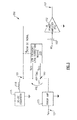
- FIG 1 is a schematic diagram of an example PA operating configuration 100 incorporating envelope tracking. While pertinent features are illustrated, those skilled in the art will appreciate that various other features have not been illustrated for the sake of brevity and so as not to obscure more pertinent aspects of the disclosed example. To that end, as a non-limiting example, the PA operating configuration 100 includes a PA 102, a DC-DC converter 115, and an error amplifier 120.
- the PA 102 is arranged to receive a RF input signal (RFin) through coupling capacitor 103 (C), and to provide an amplified RF output signal (RF out ) on output node 107.
- the capacitor 103 is implemented as a single capacitor or a multi-component capacitive circuit arrangement.
- the PA 102 also has a voltage supply node 101 provided to receive a voltage supply level that tracks the voltage envelope (i.e., the envelope signal, Venv) of the RF input signal (RF in ).
- the voltage supply node 101 is coupled to the combination of the DC-DC converter 115 and the error amplifier 120.
- the DC-DC converter 115 is coupled to the voltage supply node 101 through series inductor 116 (L 1 ).
- the DC-DC converter 115 is provided to supply a DC voltage level to the PA 102 that coarsely tracks the envelope signal (V env ).
- the DC-DC converter 115 coarsely tracks the envelope signal (V env ) by switching between DC voltage levels supplied to the inputs 114 of the DC-DC converter 115.
- the error amplifier 120 is provided to supply the substantially AC voltage envelope signal (V env ) to the voltage supply node 101 of the PA 102.
- a capacitor 125 (C BIG ) is used to couple the envelope signal (V env ) to the voltage supply node 101.
- a drawback associated with this arrangement is that lower frequency components of the envelope signal (V env ) are blocked by the coupling capacitor 125 (C BIG ) due to the finite value of capacitance.
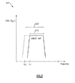
- Figure 2 is a performance diagram 200 illustrating a pass band 210 within which portions of the envelope signal (V env ) are applied to the supply of the PA 102 shown in Figure 1 .
- the envelope signal (V env ) provided by the error amplifier 120 has a bandwidth 220 with a lower cutoff frequency f c2 .
- the capacitor 125 (C BIG ) creates the pass band 210, having a lower cutoff frequency f c1 , that substantially blocks lower frequency components of the envelope signal (V env ) below the lower cutoff frequency f c1 .
- the capacitor 125 (C BIG ) substantially creates a pass band filter with the pass band 210 that is smaller than bandwidth 220 of the envelope signal (V env ). Consequently, at least one of efficiency and linearity of the PA 102 may not benefit to the extent possible because the lower frequency components are substantially blocked by the coupling capacitor 125 (C BIG ).
- FIG. 3 is a schematic diagram of a PA operating configuration 300 that incorporates low frequency envelope tracking according to some implementations.
- the PA operating configuration 300 illustrated in Figure 3 is similar to and adapted from the PA operating configuration 100 illustrated in Figure 1 . Elements common to each include common reference numbers, and only the differences between Figures 1 and 3 are described herein for the sake of brevity.
- the PA operating configuration 300 includes a low frequency loss correction module 310.
- the low frequency loss correction module 310 is configured to detect a low frequency portion of the envelope signal (V env ) that is substantially attenuated or lost through the coupling capacitor 125 (C BIG ), and to responsively provide a low frequency correction signal to the voltage supply node 101.
- the low frequency loss correction module 310 is configured to sense low frequency voltage component drop across the coupling capacitor 125 (C BIG ), which is used as an error signal.
- the low frequency loss correction module 310 includes a signal error detection circuit that is configured to detect one or more frequency components of an envelope signal below a cutoff frequency that are substantially attenuated through a capacitive path.
- the signal error detection circuit includes a comparator configured to produce an error signal as a function of respective first and second voltage signals sensed across the capacitive path (e.g., the coupling capacitor 125, C BIG ). The error signal is used to generate a low frequency correction signal that is supplied to the voltage supply node 101 of the PA 102.
- the low frequency loss correction module 310 includes a drive circuit configured to convert the error signal into a low frequency loss correction signal and to provide the low frequency loss correction signal to a voltage supply line of a power amplifier. In this manner the PA 102 is able to benefit from envelope tracking at lower frequencies, because previously attenuated or lost lower frequency envelope signal (V env ) components are now provided to the voltage supply node 101. In some implementations, PA efficiency benefits from envelope tracking at near DC frequencies using a low frequency loss correction module.
- FIG 4 is a performance diagram 400 illustrating the frequency band within which the envelope signal (V env ) passes to the PA 102 shown in Figure 3 .
- the envelope signal (V env ) provided by the error amplifier 120 has a bandwidth 420 with a lower cutoff frequency f c2 .
- the capacitor 125 (C BIG ) substantially blocks lower frequency components of the envelope signal (V env ), and substantially passes frequency components that are above a lower cutoff frequency f c1 to the voltage supply node 101 of the PA 102. In other words, the capacitor 125 (C BIG ) substantially limits the bandwidth of passable frequencies.
- the operation of the low frequency loss correction module 310 extends the lower range of frequency components of the envelope signal (V env ) to at least the lower cutoff frequency f c2 , enabling PA efficiency and/or linearity to benefit from envelope tracking at frequencies below the lower cutoff frequency f c1 established by the coupling capacitor 125 (C BIG ).
- FIG 5 is a schematic diagram of a PA operating configuration 500 that includes low frequency envelope tracking in accordance with some implementations.
- the PA operating configuration 500 is similar to and adapted from the PA operating configuration 300 illustrated in Figure 3 .
- Elements common to each include common reference numbers, and only the differences between Figures 3 and 5 are described herein for the sake of brevity.
- the error amplifier 120 shown in Figure 5 includes a differential amplifier 520 (e.g., an op-amp), a voltage divider including first and second resistors 523, 524, and a third resistor 526.
- the first, second and third resistors 523, 524, 526 set the feedback gain of the error amplifier 520.
- the first and second resistors 523, 524 are coupled in series between the voltage supply node 101 and a first input node 521.
- the third resistor 526 is coupled between the output node and the negative input node of the differential amplifier 520.
- the first input node 521 is provided to receive the envelope signal (V env ) associated with the RF input signal (RFin) amplified by the PA 102.
- the node 525 coupling the first and second resistors 523, 524 is also coupled to the negative input node of the differential amplifier 520.
- a second input node 522 is coupled to the positive input node of the differential amplifier 520, and is provided to receive a first reference signal (V ref1 ).
- the output of the differential amplifier 520 is coupled to the AC coupling capacitor 125 (C BIG ).
- the output of the differential amplifier 520 is also coupled to provide a current, I sense , to the hysteretic comparator 540.
- the PA operating configuration 500 includes an implementation of a low frequency loss correction module 510 arranged in a manner similar to the low frequency loss correction module 310 of Figure 3 .
- the low frequency loss correction module 510 includes a signal error detection circuit 510a and a drive circuit 510b.
- the signal error detection circuit 510a is configured to detect one or more frequency components of an envelope signal below a cutoff frequency that are substantially attenuated through a capacitive path.
- the signal error detection circuit 510a includes a comparator 514 that is configured to produce an error signal as a function of respective first and second voltage signals sensed across the coupling capacitor 125 (C BIG ).
- the error signal is provided to the drive circuit 510b through resistor 516.
- a reference signal is provided to the drive circuit 510b through resistor 517.
- the reference signal is provided by a combination of a voltage source 530 and a comparator 515.
- the drive circuit 510b includes a differential amplifier 511, a nominal current source (I o ) 561 and a controllable current source (I CTRL ) 563.
- the nominal current source (I o ) 561 and the controllable current source (I CTRL ) 563 are coupled in parallel between node 525 and ground.
- the negative input of the differential amplifier 511 is coupled to receive the respective error signal through the corresponding resistors 516, 517.
- the negative input of the differential amplifier 511 is coupled to receive a second reference signal (V ref2 ).
- a capacitor 512 is coupled across the negative input and output of the differential amplifier 511.
- the output of the differential amplifier 511 is used to control the controllable current source (I CTRL ) 563, which serves as an output of the low frequency loss correction module 510.
- the comparator 514 produces an error signal as a function of respective first and second voltage signals sensed across the coupling capacitor 125 (C BIG ).
- the differential amplifier 511 is used to generate a low frequency correction signal using the error signal and the reference signal.
- the low frequency correction signal is supplied to the voltage supply node 101 of the PA 102 through the controllable current source (I CTRL ) 563 and the voltage divider included in the error amplifier 120.
- I CTRL controllable current source
- the PA 102 is able to benefit from envelope tracking at lower frequencies, because the lower frequency envelope signal (V env ) components that are attenuated or lost through the coupling capacitor 125 (C BIG ) are now provided to the voltage supply node 101 by the low frequency loss correction module 510.
- PA efficiency benefits from envelope tracking at near DC frequencies using a low frequency loss correction module.
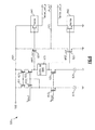
- FIG. 6 is a schematic drawing of an implementation of the differential amplifier 520 of Figure 5 .
- the differential amplifier 520 includes first and second PMOS transistors 611, 612 coupled drain-to-source between a voltage supply (VDD) 601 and the drain of a first NMOS transistor 613.
- the source of the first NMOS transistor 613 is coupled to a first current source 614, which is ultimately coupled to ground.
- the differential amplifier 520 also includes third and fourth PMOS transistors 621, 622 coupled drain-to-source between a voltage supply (VDD) 601 and a class AB bias circuit 625.
- the class AB bias circuit 625 is also coupled to the drain of a second NMOS transistor 623.
- the source of the second NMOS transistor 623 is coupled to a second current source 624, which is ultimately coupled to ground.
- the drain of the first NMOS transistor 613 is coupled to the gates of the first and third PMOS transistors 611, 621.
- the gates of the second and fourth PMOS transistors 612, 622 are coupled to an input bias voltage V bias1 .
- the gates of the first and second NMOS transistors 613, 623 are coupled to an input bias voltage V bias2 .
- the differential amplifier 520 also includes an output PMOS transistor 631 and an output NMOS transistor 633, which are coupled drain-to-drain between the voltage supply (VDD) 601 and ground.
- the gate of the output PMOS transistor 631 is coupled to the drain of the fourth PMOS transistor 622.
- the gate of the output NMOS transistor 633 is coupled to the drain of the second NMOS transistor 623.
- the primary output node 651 of the differential amplifier is taken from the drains of the output PMOS transistor 631 and the output NMOS transistor 633.
- the differential amplifier 520 also has a current sense PMOS transistor 641, and a current sense NMOS transistor 642.
- the source of the current sense PMOS transistor 641 is coupled to the voltage supply (VDD) 601, and the gate is coupled to the drain of the fourth PMOS transistor 622.
- a first current sense output is taken from the drain of the current sense PMOS transistor 641.
- the source of the current sense NMOS transistor 642 is coupled to ground, and the gate is coupled to the drain of the second NMOS transistor 623.
- a second current sense output is taken from the drain of the current sense NMOS transistor 642.
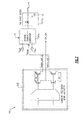
- FIG 7 is a schematic diagram 700 of the differential amplifier 520 and hysteretic comparator 540 of Figure 5 .
- the hysteretic comparator 540 includes a current comparator 540a and a low pass filter 540b coupled in series.
- the current comparator 540a is coupled to receive the differential current I sense from the differential amplifier 520.
- the positive and negative currents flowing out of differential amplifier 520 are sensed by I sense_out_p and I sense_out_n , and compared to determine the rise or fall of the average DC-DC voltage.
- a current comparator is utilized to perform the comparison.
- the output of the comparator 540a is then conditioned by the low pass filter 540b in order to obtain the voltage applied to correct the DC voltage provided by DC-DC converter 115. That is, the resulting signal is coupled back to the input of the DC to DC convertor thereby closing the feedback loop.
- the comparator 540a in order to avoid oscillations the comparator 540a is a hysteretic comparator, having upper and lower limits I high and I low . If the current difference (i.e., I high - I low ) is high, less high frequency content is obtained. Thus, in combination with the low pass filter 540b a preferred filter characteristic is produced.
- Figure 8 is a flowchart of an implementation of a method 800 of correcting low frequency component loss associated with coupling an envelope signal to the voltage supply of a power amplifier through a capacitive path.
- method 800 is performed by a power management system and/or controller associated with a power amplifier.
- method 800 includes detecting a low frequency portion of an envelope signal that is substantially attenuated or lost through a capacitive path, and responsively providing a low frequency correction signal to a voltage supply node of a power amplifier.
- method 800 includes detecting low frequency component loss of an envelope signal through a capacitive path.
- the method 800 includes sensing voltage signals on respective terminals of the coupling capacitor (C SIG ).
- the method 800 includes generating an error signal that is representative of low frequency component loss.
- the method 800 includes determining the component difference between the voltage signals sensed across the coupling capacitor (C BIG ), in order to detect low frequency component loss, by using the comparator 514.
- the method 800 includes converting the error voltage signal into a loss correction signal.
- the method 800 includes producing the loss correction signal using the differential amplifier 511.
- the method 800 includes combining or adding the loss correction signal to the voltage supply line of the power amplifier.
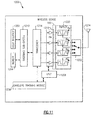
- Figures 9A-9C are schematic diagrams of different integrated circuit implementations of the low frequency loss correction module 510 of Figure 5 . While some example features are illustrated, those skilled in the art will appreciate from the present disclosure that various other features have not been illustrated for the sake of brevity and so as not to obscure more pertinent aspects of the example implementations disclosed herein. To that end, for example, Figure 9A shows that in some implementations, some or all portions of the low frequency loss correction module 510 can be part of a semiconductor die 1000. By way of an example, the low frequency loss correction module 510 can be formed on a substrate 1002 of the die 1000. A plurality of connection pads 1004 can also be formed on the substrate 1002 to facilitate functionalities associated with some or all portions of the low frequency loss correction module 510.
- Figure 9B shows that in some implementations, a semiconductor die 1000 having a substrate 1002 can include some or all portions of the error amplifier 120 and some or all portions of the low frequency loss correction module 510 of Figure 5 .
- a plurality of connection pads 1004 can also be formed on the substrate 1002 to facilitate functionalities associated with some or all portions of the error amplifier 120 and some or all portions of the low frequency loss correction module 510 of Figure 5 .
- Figure 9C shows that in some implementations, a semiconductor die 1000 having a substrate 1002 can include some or all portions of the PA circuit 102, some or all portions of the error amplifier 120 and some or all portions of the low frequency loss correction module 510 of Figure 5 .
- a plurality of connection pads 1004 can also be formed on the substrate 1002 to facilitate functionalities associated with some or all portions of the PA circuit 102, the error amplifier 120, and the low frequency loss correction module 510.
- FIG. 10 is a schematic diagram of an implementation of a module 1100 including the low frequency loss correction module 510 of Figure 5 . While some example features are illustrated, those skilled in the art will appreciate from the present disclosure that various other features have not been illustrated for the sake of brevity and so as not to obscure more pertinent aspects of the example implementations disclosed herein.
- the module 1100 includes a packaging substrate 1152, connection pads 1156, a CMOS (complementary metal oxide semiconductor) die 1000, a HBT (heterojunction bipolar transistor) die 1110, a matching network 108, and one or more surface mount devices 1160.
- CMOS complementary metal oxide semiconductor
- HBT heterojunction bipolar transistor
- the CMOS die 1000 includes a substrate 1002 including some or all portions of the error amplifier 120 and some or all portions of the low frequency loss correction module 510 of Figure 5 .
- a plurality of connection pads 1004 is formed on the substrate 1002 to facilitate functionalities associated with some or all portions of the error amplifier 120 and some or all portions of the low frequency loss correction module 510 of Figure 5 .
- the HBT die 1110 includes a substrate 1102 including some or all portions of the PA 102 and some or all portions of the bias circuitry provided to set the quiescent conditions of the PA 102.
- the HBT die 1110 also includes a plurality of connection pads 1104 formed on the substrate 1102 to facilitate functionalities associated with some or all portions of the PA 102 and some or all portions of the bias circuitry 1103.
- connection pads 1156 on the packaging substrate 1152 facilitate electrical connections to and from each of the CMOS die 1000 and the HBT die 1110.
- the connection pads 1156 facilitate the use of wirebonds 1154 for passing various signals and supply currents and/or voltages to each of the CMOS die 1000 and the HBT die 1110.
- the components mounted on the packaging substrate 1152 or formed on or in the packaging substrate 1152 can further include, for example, one or more surface mount devices (SMDs) (e.g., 1160) and one or more matching networks (e.g., 108).
- the packaging substrate 1152 can include a laminate substrate.
- the module 1100 can also include one or more packaging structures to, for example, provide protection and facilitate easier handling of the module 1100.
- a packaging structure can include an overmold formed over the packaging substrate 1152 and dimensioned to substantially encapsulate the various circuits and components thereon.
- module 1100 is described in the context of wirebond-based electrical connections, one or more features of the present disclosure can also be implemented in other packaging configurations, including flip-chip configurations.
- a device and/or a circuit having one or more features described herein can be included in an RF device such as a wireless device.
- a wireless device such as a wireless device.
- Such a device and/or a circuit can be implemented directly in the wireless device, in a modular form as described herein, or in some combination thereof.
- such a wireless device can include, for example, a cellular phone, a smart-phone, a hand-held wireless device with or without phone functionality, a wireless tablet, a wireless router, a wireless access point, a wireless base station, etc.
- the low frequency loss correction module may be included in various devices, such as a computer, a laptop computer, a tablet device, a netbook, an internet kiosk, a personal digital assistant, an optical modem, a base station, a repeater, a wireless router, a mobile phone, a smartphone, a gaming device, a computer server, or any other computing device.
- such devices include one or more processors, one or more types of memory, a display and/or other user interface components such as a keyboard, a touch screen display, a mouse, a track-pad, a digital camera and/or any number of supplemental devices to add functionality.
- Figure 11 is a schematic diagram of an implementation of a wireless device 1200 including one or more features described herein, such as the low frequency loss correction module 510 of Figure 5 . While some example features are illustrated, those skilled in the art will appreciate from the present disclosure that various other features have not been illustrated for the sake of brevity and so as not to obscure more pertinent aspects of the example implementations disclosed herein.
- One or more PAs 1216 as described herein are biased by respective bias circuit(s) (not shown) and compensated by respective compensation circuit(s) (not shown).
- the PAs 1216 are packaged into a module including matching circuits 100.
- the PAs 1216 can receive respective RF signals from a transceiver 1214, that can be configured and operated in known manners to generate RF signals to be amplified and transmitted, and to process received signals.
- the transceiver 1214 is shown to interact with a baseband sub-system 1210 that is configured to provide conversion between data and/or voice signals suitable for a user and RF signals suitable for the transceiver 1214.
- the transceiver 1214 is also shown to be connected to an envelope tracking module 1206 that is configured to manage power for the operation of the wireless device 1200. Such power management can also control operations of the baseband sub-system 1210, and the low frequency loss correction module 1208 coupled to the PAs 1216.
- the baseband sub-system 1210 is shown to be connected to a user interface 1202 to facilitate various input and output of voice and/or data provided to and received from the user.
- the baseband sub-system 1210 can also be connected to a memory 1204 that is configured to store data and/or instructions to facilitate the operation of the wireless device, and/or to provide storage of information for the user.
- outputs of the PAs 1216 are shown to be matched and routed to an antenna 1224 via respective duplexers 1220 and a band-selection switch 1222.
- the band-selection switch 1222 can include, for example, a single-pole-multiple-throw (e.g., SP4T) switch to allow selection of an operating band (e.g., Band 2).
- each duplexer 1220 can allow transmit and receive operations to be performed simultaneously using a common antenna (e.g., 1224).
- a wireless device does not need to be a multi-band device.
- a wireless device can include additional antennas such as diversity antenna, and additional connectivity features such as Wi-Fi, Bluetooth, and GPS.
- the order of the steps and/or phases can be rearranged and certain steps and/or phases may be omitted entirely.
- the methods described herein are to be understood to be open-ended, such that additional steps and/or phases to those shown and described herein can also be performed.
- Computer software can comprise computer executable code stored in a computer readable medium (e.g., non-transitory computer readable medium) that, when executed, performs the functions described herein.
- computer-executable code is executed by one or more general purpose computer processors.
- any feature or function that can be implemented using software to be executed on a general purpose computer can also be implemented using a different combination of hardware, software, or firmware.
- such a module can be implemented completely in hardware using a combination of integrated circuits.
- such a feature or function can be implemented completely or partially using specialized computers designed to perform the particular functions described herein rather than by general purpose computers.
- distributed computing devices can be substituted for any one computing device described herein.
- the functions of the one computing device are distributed (e.g., over a network) such that some functions are performed on each of the distributed computing devices.
- any such computer program instructions may be loaded onto one or more computers, including without limitation a general purpose computer or special purpose computer, or other programmable processing apparatus to produce a machine, such that the computer program instructions which execute on the computer(s) or other programmable processing device(s) implement the functions specified in the equations, algorithms, and/or flowcharts. It will also be understood that each equation, algorithm, and/or block in flowchart illustrations, and combinations thereof, may be implemented by special purpose hardware-based computer systems which perform the specified functions or steps, or combinations of special purpose hardware and computer-readable program code logic means.
- computer program instructions such as embodied in computer-readable program code logic, may also be stored in a computer readable memory (e.g., a non-transitory computer readable medium) that can direct one or more computers or other programmable processing devices to function in a particular manner, such that the instructions stored in the computer-readable memory implement the function(s) specified in the block(s) of the flowchart(s).
- a computer readable memory e.g., a non-transitory computer readable medium
- the computer program instructions may also be loaded onto one or more computers or other programmable computing devices to cause a series of operational steps to be performed on the one or more computers or other programmable computing devices to produce a computer-implemented process such that the instructions which execute on the computer or other programmable processing apparatus provide steps for implementing the functions specified in the equation(s), algorithm(s), and/or block(s) of the flowchart(s).
- the computer system may, in some cases, include multiple distinct computers or computing devices (e.g., physical servers, workstations, storage arrays, etc.) that communicate and interoperate over a network to perform the described functions.
- Each such computing device typically includes a processor (or multiple processors) that executes program instructions or modules stored in a memory or other non-transitory computer-readable storage medium or device.
- the various functions disclosed herein may be embodied in such program instructions, although some or all of the disclosed functions may alternatively be implemented in application-specific circuitry (e.g., ASICs or FPGAs) of the computer system. Where the computer system includes multiple computing devices, these devices may, but need not, be co-located.
- the results of the disclosed methods and tasks may be persistently stored by transforming physical storage devices, such as solid state memory chips and/or magnetic disks, into a different state.
Landscapes
- Engineering & Computer Science (AREA)
- Power Engineering (AREA)
- Microelectronics & Electronic Packaging (AREA)
- Amplifiers (AREA)
- Computer Networks & Wireless Communication (AREA)
- Signal Processing (AREA)
Abstract
Description
- The present disclosure generally relates to wireless communication systems and, more specifically, to improving the efficiency of power amplifiers therein.
- Power amplifiers are widely used in various communication networks to set the transmission power level of an information-bearing signal transmitted by a device. For example, power amplifiers are used to set the pulse energy emitted by pulsed lasers in optical communication networks. Power amplifiers are also used in the radio frequency (RF) front end components of wireless carrier network devices - such as base stations, repeaters, and mobile devices - to set the power level of a signal transmitted through an antenna. Power amplifiers are also used in local area networks to support both wired and wireless connectivity of servers, computers, laptops, and peripheral devices.
- Managing the operation of a power amplifier is often of particular interest in mobile devices. The efficiency of a power amplifier is often a leading factor in the efficiency of a RF front end, and in turn, battery life of a mobile device. Envelope tracking can be used to improve power amplifier efficiency. Envelope tracking includes adapting the voltage supply level provided to a power amplifier in relation to the envelope of the RF signal amplified by the power amplifier. In other words, the voltage supply level provided to a power amplifier increases in response to increases of the envelope of the RF signal. Likewise, the voltage supply level decreases in response to decreases of the envelope of the RF signal. Having the voltage supply level track the envelope of the RF signal reduces the peak-to-average voltage drop ratio across the power amplifier, and in turn, reduces the current drawn by the power amplifier. Envelope tracking is particularly useful in reducing the current draw within RF signal troughs, during which current draw by the power amplifier usually peaks.
- A coupling capacitor is typically used to isolate the DC voltage level of the envelope tracking circuitry from the DC voltage supply of the power amplifier. However, because of the finite size of the coupling capacitor, near-DC low frequencies are also typically blocked by the coupling capacitor along with the DC voltage level of the envelope tracking circuitry. As a result, the efficiency of a power amplifier at near-DC low frequencies cannot be improved by envelop tracking using known methods and circuit arrangements because of the finite limitations of coupling capacitors.
- The invention, in its various aspects is defined by the independent claims to which reference is directed.
- In accordance with some implementations, the present disclosure relates to a low frequency loss correction circuit that improves the efficiency of a power amplifier at near-DC low frequencies The low frequency loss correction circuit can include a signal error detection circuit configured to produce an error signal in response to detecting one or more frequency components of a tracking signal below a cutoff frequency that are substantially attenuated through a capacitive path. The low frequency loss correction circuit can include a drive circuit configured to convert the error signal into a low frequency correction signal, and provide the low frequency correction signal to a voltage supply line, the low frequency correction signal including at least some of the one or more frequency components of the tracking signal below a cutoff frequency that are substantially attenuated through the capacitive path.
- In some implementations, the signal error detection circuit includes first and second detection nodes connectable across the capacitive path configured to sense respective first and second signals.
- In some implementations, the signal error detection circuit includes a comparator configured to produce the error signal as a function of respective first and second signals sensed across the capacitive path.
- In some implementations, the drive circuit includes a drive transistor coupled to the voltage supply line.
- In some implementations, a terminal of the driver transistor is coupled to a portion of a voltage divider stemming from the voltage supply line.
- In some implementations, the drive circuit includes a differential amplifier arranged to produce the low frequency correction signal using the error signal and a reference signal.
- In some implementations, the controller can be included in an envelope tracking module configured to provide an envelope signal to a voltage supply of a power amplifier.
- In some implementations, the present disclosure relates to power amplifier (PA) module that includes a packaging substrate configured to receive a plurality of components. The PA module further includes power amplifier circuit provided in a die included on the packaging substrate, the power amplifier including a voltage supply line. The PA module further includes a signal error detection circuit configured to produce an error signal in response to detecting one or more frequency components of a tracking signal below a cutoff frequency that are substantially attenuated through a capacitive path coupled to the voltage supply line. The PA module further includes a drive circuit configured to convert the error signal into a low frequency correction signal, and provide the low frequency correction signal to the voltage supply line, the low frequency correction signal including at least some of the one or more frequency components of the tracking signal below a cutoff frequency that are substantially attenuated through the capacitive path.
- In some implementations, the PA module can further include a tracking circuit configured to provide the tracking signal, the tracking signal characterizing the voltage envelope of a radio frequency signal amplified by the power amplifier.
- In some implementations, the signal error detection circuit includes first and second detection nodes connectable across the capacitive path configured to sense respective first and second signals.
- In some implementations, the signal error detection circuit includes a comparator configured to produce the error signal as a function of respective first and second signals sensed across the capacitive path.
- In some implementations, the drive circuit includes a drive transistor coupled to the voltage supply line.
- In some implementations, a terminal of the drive transistor is coupled to a portion of a voltage divider stemming from the voltage supply line.
- In some implementations, the drive circuit includes a differential amplifier arranged to produce the low frequency correction signal using the error signal and a reference signal.
- According to some teachings, the present disclosure relates to a wireless device that includes a power amplifier circuit including a voltage supply line. The wireless device further includes a signal error detection circuit configured to produce an error signal in response to detecting one or more frequency components of a tracking signal below a cutoff frequency that are substantially attenuated through a capacitive path coupled to the voltage supply line. The wireless device further includes a drive circuit configured to convert the error signal into a low frequency correction signal, and provide the low frequency correction signal to the voltage supply line, the low frequency correction signal including at least some of the one or more frequency components of the tracking signal below a cutoff frequency that are substantially attenuated through the capacitive path.
- In some implementations, the wireless device further includes a tracking circuit configured to provide the tracking signal, the tracking signal characterizing the voltage envelope of a radio frequency signal amplified by the power amplifier.
- In some implementations, the signal error detection circuit includes first and second detection nodes connectable across the capacitive path configured to sense respective first and second signals.
- In some implementations, the drive circuit includes a drive transistor coupled to the voltage supply line.
- In some implementations, a terminal of the drive transistor is coupled to a portion of a voltage divider stemming from the voltage supply line.
- In some implementations, the drive circuit includes a differential amplifier arranged to produce the low frequency correction signal using the error signal and a reference signal.
- According to some teachings, the present disclosure relates to a method of envelope tracking with low frequency loss correction. The method includes detecting low frequency component loss of an envelope signal through a capacitive path. The method further includes generating an error signal that is representative of low frequency component loss. The method further includes converting the error voltage signal into a loss correction signal. The method further includes adding the loss correction signal to the voltage supply line of a power amplifier.
- So that the present disclosure can be understood in greater detail, a more particular description may be had by reference to the features of various implementations, some of which are illustrated in the appended drawings. The appended drawings, however, merely illustrate the more pertinent features of the present disclosure and are therefore not to be considered limiting, for the description may admit to other effective features.
-
Figure 1 is a schematic diagram of a power amplifier operating control configuration according to some implementations. -
Figure 2 is a performance diagram illustrating the frequency band within which an envelope signal passes to the power amplifier shown inFigure 1 . -
Figure 3 is a schematic diagram of a power amplifier operating control configuration having low frequency loss correction according to some implementations. -
Figure 4 is a performance diagram illustrating the frequency band within which an envelope signal passes to the power amplifier shown inFigure 2 . -
Figure 5 is a schematic diagram of a power amplifier operating control configuration having low frequency loss correction according to some implementations. -
Figure 6 is a schematic diagram of a component of the low frequency loss correction circuit ofFigure 5 . -
Figure 7 is a schematic diagram of components of the low frequency loss correction circuit ofFigure 5 . -
Figure 8 is a flowchart of an implementation of a method of correction low frequency signal component loss in accordance with some implementations. -
Figures 9A-9C are schematic diagrams of different integrated circuit implementations of the low frequency loss correction circuit ofFigure 5 . -
Figure 10 is a schematic diagram of an implementation of a module including the low frequency loss correction ofFigure 5 . -
Figure 11 is a schematic diagram of an implementation of a wireless device including the low frequency loss correction circuit ofFigure 5 . - In accordance with common practice the various features illustrated in the drawings may not be drawn to scale. Accordingly, the dimensions of the various features may be arbitrarily expanded or reduced for clarity. In addition, some of the drawings may not depict all of the components of a given system, method or device. Finally, like reference numerals may be used to denote like features throughout the specification and figures.
- The headings provided herein, if any, are for convenience only and do not necessarily affect the scope or meaning of the claimed invention.
- Power amplifiers are used in communication networks to set the transmission level of data signals. For example, power amplifiers are used to set transmission pulse laser energy in optical communication networks. Power amplifiers are used in radio frequency (RF) components of wireless devices - e.g., base stations and mobile devices - to set the power level transmitted through an antenna. Power amplifiers are also used in local area networks to support connectivity of servers, computers, laptops, and peripheral devices.
- Managing power amplifier (PA) operation is a concern in mobile devices because the efficiency of a PA often significantly affects the battery life of a mobile device. Envelope tracking can be used to improve PA efficiency, and includes adjusting the voltage supplied to a PA in association with the envelope of the RF signal amplified by the PA. That is, the PA voltage supply is increased in response to increases in the voltage envelope of the RF signal, and the PA voltage supply is decreased in response to decreases of the envelope. In some implementations, envelope tracking improves PA efficiency by reducing the bias voltage to the PA during a signal trough. In particular, in some implementations envelope tracking is effective for systems that are used to amplify signals with large peak-to-average ratios.
-
Figure 1 is a schematic diagram of an examplePA operating configuration 100 incorporating envelope tracking. While pertinent features are illustrated, those skilled in the art will appreciate that various other features have not been illustrated for the sake of brevity and so as not to obscure more pertinent aspects of the disclosed example. To that end, as a non-limiting example, thePA operating configuration 100 includes aPA 102, a DC-DC converter 115, and anerror amplifier 120. - The
PA 102 is arranged to receive a RF input signal (RFin) through coupling capacitor 103 (C), and to provide an amplified RF output signal (RFout) onoutput node 107. In various implementations, thecapacitor 103 is implemented as a single capacitor or a multi-component capacitive circuit arrangement. - The
PA 102 also has avoltage supply node 101 provided to receive a voltage supply level that tracks the voltage envelope (i.e., the envelope signal, Venv) of the RF input signal (RFin). To that end, thevoltage supply node 101 is coupled to the combination of the DC-DC converter 115 and theerror amplifier 120. The DC-DC converter 115 is coupled to thevoltage supply node 101 through series inductor 116 (L1). The DC-DC converter 115 is provided to supply a DC voltage level to thePA 102 that coarsely tracks the envelope signal (Venv). In some implementations, the DC-DC converter 115 coarsely tracks the envelope signal (Venv) by switching between DC voltage levels supplied to the inputs 114 of the DC-DC converter 115. - The
error amplifier 120 is provided to supply the substantially AC voltage envelope signal (Venv) to thevoltage supply node 101 of thePA 102. A capacitor 125 (CBIG) is used to couple the envelope signal (Venv) to thevoltage supply node 101. With reference toFigure 2 , a drawback associated with this arrangement is that lower frequency components of the envelope signal (Venv) are blocked by the coupling capacitor 125 (CBIG) due to the finite value of capacitance.Figure 2 is a performance diagram 200 illustrating apass band 210 within which portions of the envelope signal (Venv) are applied to the supply of thePA 102 shown inFigure 1 . The envelope signal (Venv) provided by theerror amplifier 120 has abandwidth 220 with a lower cutoff frequency fc2. However, the capacitor 125 (CBIG) creates thepass band 210, having a lower cutoff frequency fc1, that substantially blocks lower frequency components of the envelope signal (Venv) below the lower cutoff frequency fc1. In other words, the capacitor 125 (CBIG) substantially creates a pass band filter with thepass band 210 that is smaller thanbandwidth 220 of the envelope signal (Venv). Consequently, at least one of efficiency and linearity of thePA 102 may not benefit to the extent possible because the lower frequency components are substantially blocked by the coupling capacitor 125 (CBIG). - By contrast, the various implementations described herein include systems, methods and devices configured to enable more desirable power amplifier operation at lower frequencies by correcting for low frequency envelope signal losses. To that end,
Figure 3 is a schematic diagram of aPA operating configuration 300 that incorporates low frequency envelope tracking according to some implementations. ThePA operating configuration 300 illustrated inFigure 3 is similar to and adapted from thePA operating configuration 100 illustrated inFigure 1 . Elements common to each include common reference numbers, and only the differences betweenFigures 1 and3 are described herein for the sake of brevity. In particular, thePA operating configuration 300 includes a low frequencyloss correction module 310. Briefly, the low frequencyloss correction module 310 is configured to detect a low frequency portion of the envelope signal (Venv) that is substantially attenuated or lost through the coupling capacitor 125 (CBIG), and to responsively provide a low frequency correction signal to thevoltage supply node 101. - More specifically, the low frequency
loss correction module 310 is configured to sense low frequency voltage component drop across the coupling capacitor 125 (CBIG), which is used as an error signal. In some implementations, the low frequencyloss correction module 310 includes a signal error detection circuit that is configured to detect one or more frequency components of an envelope signal below a cutoff frequency that are substantially attenuated through a capacitive path. In some implementations, the signal error detection circuit includes a comparator configured to produce an error signal as a function of respective first and second voltage signals sensed across the capacitive path (e.g., thecoupling capacitor 125, CBIG). The error signal is used to generate a low frequency correction signal that is supplied to thevoltage supply node 101 of thePA 102. In some implementations, the low frequencyloss correction module 310 includes a drive circuit configured to convert the error signal into a low frequency loss correction signal and to provide the low frequency loss correction signal to a voltage supply line of a power amplifier. In this manner thePA 102 is able to benefit from envelope tracking at lower frequencies, because previously attenuated or lost lower frequency envelope signal (Venv) components are now provided to thevoltage supply node 101. In some implementations, PA efficiency benefits from envelope tracking at near DC frequencies using a low frequency loss correction module. -
Figure 4 is a performance diagram 400 illustrating the frequency band within which the envelope signal (Venv) passes to thePA 102 shown inFigure 3 . As described above, the envelope signal (Venv) provided by theerror amplifier 120 has abandwidth 420 with a lower cutoff frequency fc2. The capacitor 125 (CBIG) substantially blocks lower frequency components of the envelope signal (Venv), and substantially passes frequency components that are above a lower cutoff frequency fc1 to thevoltage supply node 101 of thePA 102. In other words, the capacitor 125 (CBIG) substantially limits the bandwidth of passable frequencies. However, the operation of the low frequencyloss correction module 310 extends the lower range of frequency components of the envelope signal (Venv) to at least the lower cutoff frequency fc2, enabling PA efficiency and/or linearity to benefit from envelope tracking at frequencies below the lower cutoff frequency fc1 established by the coupling capacitor 125 (CBIG). -
Figure 5 is a schematic diagram of aPA operating configuration 500 that includes low frequency envelope tracking in accordance with some implementations. ThePA operating configuration 500 is similar to and adapted from thePA operating configuration 300 illustrated inFigure 3 . Elements common to each include common reference numbers, and only the differences betweenFigures 3 and5 are described herein for the sake of brevity. - The
error amplifier 120 shown inFigure 5 includes a differential amplifier 520 (e.g., an op-amp), a voltage divider including first andsecond resistors third resistor 526. The first, second andthird resistors error amplifier 520. The first andsecond resistors voltage supply node 101 and afirst input node 521. Thethird resistor 526 is coupled between the output node and the negative input node of thedifferential amplifier 520. Thefirst input node 521 is provided to receive the envelope signal (Venv) associated with the RF input signal (RFin) amplified by thePA 102. Thenode 525 coupling the first andsecond resistors differential amplifier 520. Asecond input node 522 is coupled to the positive input node of thedifferential amplifier 520, and is provided to receive a first reference signal (Vref1). The output of thedifferential amplifier 520 is coupled to the AC coupling capacitor 125 (CBIG). The output of thedifferential amplifier 520 is also coupled to provide a current, Isense, to thehysteretic comparator 540. - The
PA operating configuration 500 includes an implementation of a low frequencyloss correction module 510 arranged in a manner similar to the low frequencyloss correction module 310 ofFigure 3 . The low frequencyloss correction module 510 includes a signalerror detection circuit 510a and adrive circuit 510b. The signalerror detection circuit 510a is configured to detect one or more frequency components of an envelope signal below a cutoff frequency that are substantially attenuated through a capacitive path. To that end, the signalerror detection circuit 510a includes acomparator 514 that is configured to produce an error signal as a function of respective first and second voltage signals sensed across the coupling capacitor 125 (CBIG). The error signal is provided to thedrive circuit 510b throughresistor 516. Similarly, a reference signal is provided to thedrive circuit 510b throughresistor 517. In some implementations, as shown inFigure 5 , the reference signal is provided by a combination of avoltage source 530 and acomparator 515. - The
drive circuit 510b includes adifferential amplifier 511, a nominal current source (Io) 561 and a controllable current source (ICTRL) 563. The nominal current source (Io) 561 and the controllable current source (ICTRL) 563 are coupled in parallel betweennode 525 and ground. The negative input of thedifferential amplifier 511 is coupled to receive the respective error signal through the correspondingresistors differential amplifier 511 is coupled to receive a second reference signal (Vref2). Acapacitor 512 is coupled across the negative input and output of thedifferential amplifier 511. The output of thedifferential amplifier 511 is used to control the controllable current source (ICTRL) 563, which serves as an output of the low frequencyloss correction module 510. - In operation, the
comparator 514 produces an error signal as a function of respective first and second voltage signals sensed across the coupling capacitor 125 (CBIG). Thedifferential amplifier 511 is used to generate a low frequency correction signal using the error signal and the reference signal. The low frequency correction signal is supplied to thevoltage supply node 101 of thePA 102 through the controllable current source (ICTRL) 563 and the voltage divider included in theerror amplifier 120. In this manner thePA 102 is able to benefit from envelope tracking at lower frequencies, because the lower frequency envelope signal (Venv) components that are attenuated or lost through the coupling capacitor 125 (CBIG) are now provided to thevoltage supply node 101 by the low frequencyloss correction module 510. In some implementations, PA efficiency benefits from envelope tracking at near DC frequencies using a low frequency loss correction module. -
Figure 6 is a schematic drawing of an implementation of thedifferential amplifier 520 ofFigure 5 . Thedifferential amplifier 520 includes first andsecond PMOS transistors 611, 612 coupled drain-to-source between a voltage supply (VDD) 601 and the drain of afirst NMOS transistor 613. The source of thefirst NMOS transistor 613 is coupled to a firstcurrent source 614, which is ultimately coupled to ground. Similarly, thedifferential amplifier 520 also includes third andfourth PMOS transistors 621, 622 coupled drain-to-source between a voltage supply (VDD) 601 and a classAB bias circuit 625. The classAB bias circuit 625 is also coupled to the drain of asecond NMOS transistor 623. The source of thesecond NMOS transistor 623 is coupled to a secondcurrent source 624, which is ultimately coupled to ground. The drain of thefirst NMOS transistor 613 is coupled to the gates of the first andthird PMOS transistors second NMOS transistors - The
differential amplifier 520 also includes anoutput PMOS transistor 631 and anoutput NMOS transistor 633, which are coupled drain-to-drain between the voltage supply (VDD) 601 and ground. The gate of theoutput PMOS transistor 631 is coupled to the drain of the fourth PMOS transistor 622. The gate of theoutput NMOS transistor 633 is coupled to the drain of thesecond NMOS transistor 623. Theprimary output node 651 of the differential amplifier is taken from the drains of theoutput PMOS transistor 631 and theoutput NMOS transistor 633. - Additionally, the
differential amplifier 520 also has a currentsense PMOS transistor 641, and a currentsense NMOS transistor 642. The source of the currentsense PMOS transistor 641 is coupled to the voltage supply (VDD) 601, and the gate is coupled to the drain of the fourth PMOS transistor 622. A first current sense output is taken from the drain of the currentsense PMOS transistor 641. Similarly, the source of the currentsense NMOS transistor 642 is coupled to ground, and the gate is coupled to the drain of thesecond NMOS transistor 623. A second current sense output is taken from the drain of the currentsense NMOS transistor 642. -
Figure 7 is a schematic diagram 700 of thedifferential amplifier 520 andhysteretic comparator 540 ofFigure 5 . Thehysteretic comparator 540 includes acurrent comparator 540a and alow pass filter 540b coupled in series. Thecurrent comparator 540a is coupled to receive the differential current Isense from thedifferential amplifier 520. In operation, the positive and negative currents flowing out ofdifferential amplifier 520 are sensed by Isense_out_p and Isense_out_n, and compared to determine the rise or fall of the average DC-DC voltage. In some implementations, a current comparator is utilized to perform the comparison. The output of thecomparator 540a is then conditioned by thelow pass filter 540b in order to obtain the voltage applied to correct the DC voltage provided by DC-DC converter 115. That is, the resulting signal is coupled back to the input of the DC to DC convertor thereby closing the feedback loop. In some implementations, in order to avoid oscillations thecomparator 540a is a hysteretic comparator, having upper and lower limits Ihigh and Ilow. If the current difference (i.e., Ihigh - Ilow) is high, less high frequency content is obtained. Thus, in combination with thelow pass filter 540b a preferred filter characteristic is produced. -
Figure 8 is a flowchart of an implementation of amethod 800 of correcting low frequency component loss associated with coupling an envelope signal to the voltage supply of a power amplifier through a capacitive path. In some implementations,method 800 is performed by a power management system and/or controller associated with a power amplifier. Briefly,method 800 includes detecting a low frequency portion of an envelope signal that is substantially attenuated or lost through a capacitive path, and responsively providing a low frequency correction signal to a voltage supply node of a power amplifier. - To that end, as represented by block 8-1,
method 800 includes detecting low frequency component loss of an envelope signal through a capacitive path. For example, as represented by block 8-1 a and with further reference toFigure 5 , themethod 800 includes sensing voltage signals on respective terminals of the coupling capacitor (CSIG). As represented by block 8-2, themethod 800 includes generating an error signal that is representative of low frequency component loss. For example, as represented by block 8-2a and with further reference toFigure 5 , themethod 800 includes determining the component difference between the voltage signals sensed across the coupling capacitor (CBIG), in order to detect low frequency component loss, by using thecomparator 514. As represented by block 8-3, themethod 800 includes converting the error voltage signal into a loss correction signal. For example, as represented by block 8-3a and with further reference toFigure 5 , themethod 800 includes producing the loss correction signal using thedifferential amplifier 511. As represented by block 8-4, themethod 800 includes combining or adding the loss correction signal to the voltage supply line of the power amplifier. -
Figures 9A-9C are schematic diagrams of different integrated circuit implementations of the low frequencyloss correction module 510 ofFigure 5 . While some example features are illustrated, those skilled in the art will appreciate from the present disclosure that various other features have not been illustrated for the sake of brevity and so as not to obscure more pertinent aspects of the example implementations disclosed herein. To that end, for example,Figure 9A shows that in some implementations, some or all portions of the low frequencyloss correction module 510 can be part of asemiconductor die 1000. By way of an example, the low frequencyloss correction module 510 can be formed on asubstrate 1002 of thedie 1000. A plurality ofconnection pads 1004 can also be formed on thesubstrate 1002 to facilitate functionalities associated with some or all portions of the low frequencyloss correction module 510. -
Figure 9B shows that in some implementations, asemiconductor die 1000 having asubstrate 1002 can include some or all portions of theerror amplifier 120 and some or all portions of the low frequencyloss correction module 510 ofFigure 5 . A plurality ofconnection pads 1004 can also be formed on thesubstrate 1002 to facilitate functionalities associated with some or all portions of theerror amplifier 120 and some or all portions of the low frequencyloss correction module 510 ofFigure 5 . -
Figure 9C shows that in some implementations, asemiconductor die 1000 having asubstrate 1002 can include some or all portions of thePA circuit 102, some or all portions of theerror amplifier 120 and some or all portions of the low frequencyloss correction module 510 ofFigure 5 . A plurality ofconnection pads 1004 can also be formed on thesubstrate 1002 to facilitate functionalities associated with some or all portions of thePA circuit 102, theerror amplifier 120, and the low frequencyloss correction module 510. - In some implementations, one or more features described herein can be included in a module.
Figure 10 is a schematic diagram of an implementation of amodule 1100 including the low frequencyloss correction module 510 ofFigure 5 . While some example features are illustrated, those skilled in the art will appreciate from the present disclosure that various other features have not been illustrated for the sake of brevity and so as not to obscure more pertinent aspects of the example implementations disclosed herein. Themodule 1100 includes apackaging substrate 1152,connection pads 1156, a CMOS (complementary metal oxide semiconductor) die 1000, a HBT (heterojunction bipolar transistor) die 1110, amatching network 108, and one or moresurface mount devices 1160. - The CMOS die 1000 includes a
substrate 1002 including some or all portions of theerror amplifier 120 and some or all portions of the low frequencyloss correction module 510 ofFigure 5 . A plurality ofconnection pads 1004 is formed on thesubstrate 1002 to facilitate functionalities associated with some or all portions of theerror amplifier 120 and some or all portions of the low frequencyloss correction module 510 ofFigure 5 . Similarly, the HBT die 1110 includes a substrate 1102 including some or all portions of thePA 102 and some or all portions of the bias circuitry provided to set the quiescent conditions of thePA 102. The HBT die 1110 also includes a plurality of connection pads 1104 formed on the substrate 1102 to facilitate functionalities associated with some or all portions of thePA 102 and some or all portions of thebias circuitry 1103. - The
connection pads 1156 on thepackaging substrate 1152 facilitate electrical connections to and from each of the CMOS die 1000 and the HBT die 1110. For example, theconnection pads 1156 facilitate the use ofwirebonds 1154 for passing various signals and supply currents and/or voltages to each of the CMOS die 1000 and the HBT die 1110. - In some implementations, the components mounted on the
packaging substrate 1152 or formed on or in thepackaging substrate 1152 can further include, for example, one or more surface mount devices (SMDs) (e.g., 1160) and one or more matching networks (e.g., 108). In some implementations, thepackaging substrate 1152 can include a laminate substrate. - In some implementations, the
module 1100 can also include one or more packaging structures to, for example, provide protection and facilitate easier handling of themodule 1100. Such a packaging structure can include an overmold formed over thepackaging substrate 1152 and dimensioned to substantially encapsulate the various circuits and components thereon. - It will be understood that although the
module 1100 is described in the context of wirebond-based electrical connections, one or more features of the present disclosure can also be implemented in other packaging configurations, including flip-chip configurations. - In some implementations, a device and/or a circuit having one or more features described herein can be included in an RF device such as a wireless device. Such a device and/or a circuit can be implemented directly in the wireless device, in a modular form as described herein, or in some combination thereof. In some implementations, such a wireless device can include, for example, a cellular phone, a smart-phone, a hand-held wireless device with or without phone functionality, a wireless tablet, a wireless router, a wireless access point, a wireless base station, etc. That is, those skilled in the art will also appreciate from the present disclosure that in various implementations the low frequency loss correction module may be included in various devices, such as a computer, a laptop computer, a tablet device, a netbook, an internet kiosk, a personal digital assistant, an optical modem, a base station, a repeater, a wireless router, a mobile phone, a smartphone, a gaming device, a computer server, or any other computing device. In various implementations, such devices include one or more processors, one or more types of memory, a display and/or other user interface components such as a keyboard, a touch screen display, a mouse, a track-pad, a digital camera and/or any number of supplemental devices to add functionality.
-
Figure 11 is a schematic diagram of an implementation of awireless device 1200 including one or more features described herein, such as the low frequencyloss correction module 510 ofFigure 5 . While some example features are illustrated, those skilled in the art will appreciate from the present disclosure that various other features have not been illustrated for the sake of brevity and so as not to obscure more pertinent aspects of the example implementations disclosed herein. - One or more PAs 1216 as described herein are biased by respective bias circuit(s) (not shown) and compensated by respective compensation circuit(s) (not shown). In some implementations the PAs 1216 are packaged into a module including matching
circuits 100. The PAs 1216 can receive respective RF signals from atransceiver 1214, that can be configured and operated in known manners to generate RF signals to be amplified and transmitted, and to process received signals. Thetransceiver 1214 is shown to interact with abaseband sub-system 1210 that is configured to provide conversion between data and/or voice signals suitable for a user and RF signals suitable for thetransceiver 1214. Thetransceiver 1214 is also shown to be connected to anenvelope tracking module 1206 that is configured to manage power for the operation of thewireless device 1200. Such power management can also control operations of thebaseband sub-system 1210, and the low frequencyloss correction module 1208 coupled to the PAs 1216. - The
baseband sub-system 1210 is shown to be connected to auser interface 1202 to facilitate various input and output of voice and/or data provided to and received from the user. Thebaseband sub-system 1210 can also be connected to amemory 1204 that is configured to store data and/or instructions to facilitate the operation of the wireless device, and/or to provide storage of information for the user. - In the
example wireless device 1200, outputs of the PAs 1216 are shown to be matched and routed to anantenna 1224 viarespective duplexers 1220 and a band-selection switch 1222. The band-selection switch 1222 can include, for example, a single-pole-multiple-throw (e.g., SP4T) switch to allow selection of an operating band (e.g., Band 2). In some implementations, eachduplexer 1220 can allow transmit and receive operations to be performed simultaneously using a common antenna (e.g., 1224). - A number of other wireless device configurations can utilize one or more features described herein. For example, a wireless device does not need to be a multi-band device. In another example, a wireless device can include additional antennas such as diversity antenna, and additional connectivity features such as Wi-Fi, Bluetooth, and GPS.
- The present disclosure describes various features, no single one of which is solely responsible for the benefits described herein. It will be understood that various features described herein may be combined, modified, or omitted, as would be apparent to one of ordinary skill. Other combinations and subcombinations than those specifically described herein will be apparent to one of ordinary skill, and are intended to form a part of this disclosure. Various methods are described herein in connection with various flowchart steps and/or phases. It will be understood that in many cases, certain steps and/or phases may be combined together such that multiple steps and/or phases shown in the flowcharts can be performed as a single step and/or phase. Also, certain steps and/or phases can be broken into additional sub-components to be performed separately. In some instances, the order of the steps and/or phases can be rearranged and certain steps and/or phases may be omitted entirely. Also, the methods described herein are to be understood to be open-ended, such that additional steps and/or phases to those shown and described herein can also be performed.
- Some aspects of the systems and methods described herein can advantageously be implemented using, for example, computer software, hardware, firmware, or any combination of computer software, hardware, and firmware. Computer software can comprise computer executable code stored in a computer readable medium (e.g., non-transitory computer readable medium) that, when executed, performs the functions described herein. In some implementations, computer-executable code is executed by one or more general purpose computer processors. A skilled artisan will appreciate, in light of this disclosure, that any feature or function that can be implemented using software to be executed on a general purpose computer can also be implemented using a different combination of hardware, software, or firmware. For example, such a module can be implemented completely in hardware using a combination of integrated circuits. Alternatively or additionally, such a feature or function can be implemented completely or partially using specialized computers designed to perform the particular functions described herein rather than by general purpose computers.
- Multiple distributed computing devices can be substituted for any one computing device described herein. In such distributed embodiments, the functions of the one computing device are distributed (e.g., over a network) such that some functions are performed on each of the distributed computing devices.
- Some implementations may be described with reference to equations, algorithms, and/or flowchart illustrations. These methods may be implemented using computer program instructions executable on one or more computers. These methods may also be implemented as computer program products either separately, or as a component of an apparatus or system. In this regard, each equation, algorithm, block, or step of a flowchart, and combinations thereof, may be implemented by hardware, firmware, and/or software including one or more computer program instructions embodied in computer-readable program code logic. As will be appreciated, any such computer program instructions may be loaded onto one or more computers, including without limitation a general purpose computer or special purpose computer, or other programmable processing apparatus to produce a machine, such that the computer program instructions which execute on the computer(s) or other programmable processing device(s) implement the functions specified in the equations, algorithms, and/or flowcharts. It will also be understood that each equation, algorithm, and/or block in flowchart illustrations, and combinations thereof, may be implemented by special purpose hardware-based computer systems which perform the specified functions or steps, or combinations of special purpose hardware and computer-readable program code logic means.
- Furthermore, computer program instructions, such as embodied in computer-readable program code logic, may also be stored in a computer readable memory (e.g., a non-transitory computer readable medium) that can direct one or more computers or other programmable processing devices to function in a particular manner, such that the instructions stored in the computer-readable memory implement the function(s) specified in the block(s) of the flowchart(s). The computer program instructions may also be loaded onto one or more computers or other programmable computing devices to cause a series of operational steps to be performed on the one or more computers or other programmable computing devices to produce a computer-implemented process such that the instructions which execute on the computer or other programmable processing apparatus provide steps for implementing the functions specified in the equation(s), algorithm(s), and/or block(s) of the flowchart(s).
- Some or all of the methods and tasks described herein may be performed and fully automated by a computer system. The computer system may, in some cases, include multiple distinct computers or computing devices (e.g., physical servers, workstations, storage arrays, etc.) that communicate and interoperate over a network to perform the described functions. Each such computing device typically includes a processor (or multiple processors) that executes program instructions or modules stored in a memory or other non-transitory computer-readable storage medium or device. The various functions disclosed herein may be embodied in such program instructions, although some or all of the disclosed functions may alternatively be implemented in application-specific circuitry (e.g., ASICs or FPGAs) of the computer system. Where the computer system includes multiple computing devices, these devices may, but need not, be co-located. The results of the disclosed methods and tasks may be persistently stored by transforming physical storage devices, such as solid state memory chips and/or magnetic disks, into a different state.
- Unless the context clearly requires otherwise, throughout the description and the claims, the words "comprise," "comprising," and the like are to be construed in an inclusive sense, as opposed to an exclusive or exhaustive sense; that is to say, in the sense of "including, but not limited to." The word "coupled", as generally used herein, refers to two or more elements that may be either directly connected, or connected by way of one or more intermediate elements. Additionally, the words "herein," "above," "below," and words of similar import, when used in this application, shall refer to this application as a whole and not to any particular portions of this application. Where the context permits, words in the above Detailed Description using the singular or plural number may also include the plural or singular number respectively. The word "or" in reference to a list of two or more items, that word covers all of the following interpretations of the word: any of the items in the list, all of the items in the list, and any combination of the items in the list. The word "exemplary" is used exclusively herein to mean "serving as an example, instance, or illustration." Any implementation described herein as "exemplary" is not necessarily to be construed as preferred or advantageous over other implementations.
- The disclosure is not intended to be limited to the implementations shown herein. Various modifications to the implementations described in this disclosure may be readily apparent to those skilled in the art, and the generic principles defined herein may be applied to other implementations without departing from the spirit or scope of this disclosure. The teachings of the invention provided herein can be applied to other methods and systems, and are not limited to the methods and systems described above, and elements and acts of the various embodiments described above can be combined to provide further embodiments. Accordingly, the novel methods and systems described herein may be embodied in a variety of other forms; furthermore, various omissions, substitutions and changes in the form of the methods and systems described herein may be made without departing from the spirit of the disclosure. The accompanying claims and their equivalents are intended to cover such forms or modifications as would fall within the scope and spirit of the disclosure.
Claims (15)
- A low frequency loss correction circuit comprising:a signal error detection circuit configured to produce an error signal in response to detecting one or more frequency components of a tracking signal below a cutoff frequency that are substantially attenuated through a capacitive path; anda drive circuit configured to convert the error signal into a low frequency correction signal, and provide the low frequency correction signal to a voltage supply line, the low frequency correction signal including at least some of the one or more frequency components of the tracking signal below a cutoff frequency that are substantially attenuated through the capacitive path.
- The low frequency loss correction circuit of claim 1 wherein the signal error detection circuit includes first and second detection nodes connectable across the capacitive path configured to sense respective first and second signals.
- The low frequency loss correction circuit of claim 1 or 2 wherein the signal error detection circuit includes a comparator configured to produce the error signal as a function of respective first and second signals sensed across the capacitive path.
- The low frequency loss correction circuit of claim 1, 2 or 3 wherein the drive circuit includes a drive transistor coupled to the voltage supply line.
- The low frequency loss correction circuit of claim 4 wherein a terminal of the driver transistor is coupled to a portion of a voltage divider stemming from the voltage supply line.
- The low frequency loss correction circuit of any preceding claim wherein the drive circuit includes a differential amplifier arranged to produce the low frequency correction signal using the error signal and a reference signal.
- The low frequency loss correction circuit of any preceding claim included in an envelope tracking module configured to provide an envelope signal to a voltage supply of a power amplifier.
- A power amplifier module comprising:a packaging substrate configured to receive a plurality of components;a power amplifier circuit provided in a die included on the packaging substrate, the power amplifier including a voltage supply line;a signal error detection circuit configured to produce an error signal in response to detecting one or more frequency components of a tracking signal below a cutoff frequency that are substantially attenuated through a capacitive path coupled to the voltage supply line; anda drive circuit configured to convert the error signal into a low frequency correction signal, and provide the low frequency correction signal to the voltage supply line, the low frequency correction signal including at least some of the one or more frequency components of the tracking signal below a cutoff frequency that are substantially attenuated through the capacitive path.
- The power amplifier module of claim 8 further comprising a tracking circuit configured to provide the tracking signal, the tracking signal characterizing the voltage envelope of a radio frequency signal amplified by the power amplifier.
- The power amplifier module of claim 8 or 9 wherein the signal error detection circuit includes first and second detection nodes connectable across the capacitive path configured to sense respective first and second signals.
- The power amplifier module of claim 8, 9 or 10 wherein the signal error detection circuit includes a comparator configured to produce the error signal as a function of respective first and second signals sensed across the capacitive path.
- The power amplifier module of any of claims 8 to 11 wherein the drive circuit includes a drive transistor coupled to the voltage supply line.
- The power amplifier module of claim 12 wherein a terminal of the drive transistor is coupled to a portion of a voltage divider stemming from the voltage supply line.
- The power amplifier module of any of claims 8 to 13 wherein the drive circuit includes a differential amplifier arranged to produce the low frequency correction signal using the error signal and a reference signal.
- A wireless device comprising:a power amplifier circuit including a voltage supply line;a signal error detection circuit configured to produce an error signal in response to detecting one or more frequency components of a tracking signal below a cutoff frequency that are substantially attenuated through a capacitive path coupled to the voltage supply line; anda drive circuit configured to convert the error signal into a low frequency correction signal, and provide the low frequency correction signal to the voltage supply line, the low frequency correction signal including at least some of the one or more frequency components of the tracking signal below a cutoff frequency that are substantially attenuated through the capacitive path.
Applications Claiming Priority (1)
| Application Number | Priority Date | Filing Date | Title |
|---|---|---|---|
| US201462030224P | 2014-07-29 | 2014-07-29 |
Publications (2)
| Publication Number | Publication Date |
|---|---|
| EP2980988A1 true EP2980988A1 (en) | 2016-02-03 |
| EP2980988B1 EP2980988B1 (en) | 2018-12-26 |
Family
ID=53835887
Family Applications (1)
| Application Number | Title | Priority Date | Filing Date |
|---|---|---|---|
| EP15178690.2A Active EP2980988B1 (en) | 2014-07-29 | 2015-07-28 | Envelope tracking with low frequency loss correction |
Country Status (6)
| Country | Link |
|---|---|
| US (2) | US9831834B2 (en) |
| EP (1) | EP2980988B1 (en) |
| JP (1) | JP6427077B2 (en) |
| KR (1) | KR20160014559A (en) |
| CN (1) | CN105322894B (en) |
| TW (1) | TWI667878B (en) |
Cited By (1)
| Publication number | Priority date | Publication date | Assignee | Title |
|---|---|---|---|---|
| EP3562033A1 (en) * | 2018-04-26 | 2019-10-30 | MediaTek Inc. | Envelope tracking supply modulator topology for wide-bandwidth radio frequency transmitter |
Families Citing this family (94)
| Publication number | Priority date | Publication date | Assignee | Title |
|---|---|---|---|---|
| US9379668B1 (en) * | 2015-03-31 | 2016-06-28 | Qualcomm Incorporated | Envelope tracking circuits and methods with adaptive switching frequency |
| US10103693B2 (en) | 2015-09-30 | 2018-10-16 | Skyworks Solutions, Inc. | Power amplifier linearization system and method |
| US10110169B2 (en) | 2016-09-14 | 2018-10-23 | Skyworks Solutions, Inc. | Apparatus and methods for envelope tracking systems with automatic mode selection |
| US10361659B2 (en) | 2017-03-22 | 2019-07-23 | Intel IP Corporation | Power envelope tracker and adjustable strength DC-DC converter |
| US10181826B2 (en) | 2017-04-25 | 2019-01-15 | Qorvo Us, Inc. | Envelope tracking amplifier circuit |
| US10236831B2 (en) | 2017-05-12 | 2019-03-19 | Skyworks Solutions, Inc. | Envelope trackers providing compensation for power amplifier output load variation |
| US10615757B2 (en) | 2017-06-21 | 2020-04-07 | Skyworks Solutions, Inc. | Wide bandwidth envelope trackers |
| US10516368B2 (en) | 2017-06-21 | 2019-12-24 | Skyworks Solutions, Inc. | Fast envelope tracking systems for power amplifiers |
| US10158330B1 (en) | 2017-07-17 | 2018-12-18 | Qorvo Us, Inc. | Multi-mode envelope tracking amplifier circuit |
| US10326490B2 (en) | 2017-08-31 | 2019-06-18 | Qorvo Us, Inc. | Multi radio access technology power management circuit |
| US10530305B2 (en) | 2017-10-06 | 2020-01-07 | Qorvo Us, Inc. | Nonlinear bandwidth compression circuitry |
| US10439557B2 (en) | 2018-01-15 | 2019-10-08 | Qorvo Us, Inc. | Envelope tracking power management circuit |
| US10637408B2 (en) * | 2018-01-18 | 2020-04-28 | Qorvo Us, Inc. | Envelope tracking voltage tracker circuit and related power management circuit |
| US10742170B2 (en) | 2018-02-01 | 2020-08-11 | Qorvo Us, Inc. | Envelope tracking circuit and related power amplifier system |
| US10924072B2 (en) | 2018-03-28 | 2021-02-16 | Murata Manufacturing Co., Ltd. | Power amplification circuit |
| JP2019176454A (en) | 2018-03-28 | 2019-10-10 | 株式会社村田製作所 | Power amplification circuit |
| WO2019231922A1 (en) | 2018-05-31 | 2019-12-05 | Skyworks Solutions, Inc. | Apparatus and methods for multi-antenna communications |
| US10284238B1 (en) * | 2018-06-11 | 2019-05-07 | Texas Instruments Incorporated | DC coupled radio frequency modulator |
| US10944365B2 (en) | 2018-06-28 | 2021-03-09 | Qorvo Us, Inc. | Envelope tracking amplifier circuit |
| US10797650B2 (en) | 2018-07-24 | 2020-10-06 | Qorvo Us, Inc. | Envelope tracking amplifier apparatus |
| US10951175B2 (en) | 2018-09-04 | 2021-03-16 | Qorvo Us, Inc. | Envelope tracking circuit and related power amplifier apparatus |
| US11088618B2 (en) | 2018-09-05 | 2021-08-10 | Qorvo Us, Inc. | PWM DC-DC converter with linear voltage regulator for DC assist |
| US10911001B2 (en) | 2018-10-02 | 2021-02-02 | Qorvo Us, Inc. | Envelope tracking amplifier circuit |
| US10819287B2 (en) | 2018-10-19 | 2020-10-27 | Qorvo Us, Inc. | Multi-voltage generation circuit and related envelope tracking amplifier apparatus |
| US10903796B2 (en) | 2018-10-19 | 2021-01-26 | Qorvo Us, Inc. | Voltage generation circuit and related envelope tracking amplifier apparatus |
| US11108359B2 (en) | 2018-10-19 | 2021-08-31 | Qorvo Us, Inc. | Multi-amplifier envelope tracking circuit and related apparatus |
| US10630375B1 (en) * | 2018-10-19 | 2020-04-21 | Qorvo Us, Inc. | Envelope tracking amplifier apparatus |
| US11057012B2 (en) | 2018-10-19 | 2021-07-06 | Qorvo Us, Inc. | Distributed envelope tracking amplifier circuit and related apparatus |
| US10938351B2 (en) | 2018-10-31 | 2021-03-02 | Qorvo Us, Inc. | Envelope tracking system |
| US10985702B2 (en) | 2018-10-31 | 2021-04-20 | Qorvo Us, Inc. | Envelope tracking system |
| US11018638B2 (en) | 2018-10-31 | 2021-05-25 | Qorvo Us, Inc. | Multimode envelope tracking circuit and related apparatus |
| US10680556B2 (en) | 2018-11-05 | 2020-06-09 | Qorvo Us, Inc. | Radio frequency front-end circuit |
| US11038471B2 (en) | 2018-11-20 | 2021-06-15 | Skyworks Solutions, Inc. | Envelope tracking system with modeling of a power amplifier supply voltage filter |
| US11031909B2 (en) | 2018-12-04 | 2021-06-08 | Qorvo Us, Inc. | Group delay optimization circuit and related apparatus |
| US11082007B2 (en) | 2018-12-19 | 2021-08-03 | Qorvo Us, Inc. | Envelope tracking integrated circuit and related apparatus |
| US11146213B2 (en) | 2019-01-15 | 2021-10-12 | Qorvo Us, Inc. | Multi-radio access technology envelope tracking amplifier apparatus |
| US11025458B2 (en) * | 2019-02-07 | 2021-06-01 | Qorvo Us, Inc. | Adaptive frequency equalizer for wide modulation bandwidth envelope tracking |
| US10998859B2 (en) | 2019-02-07 | 2021-05-04 | Qorvo Us, Inc. | Dual-input envelope tracking integrated circuit and related apparatus |
| US11233481B2 (en) | 2019-02-18 | 2022-01-25 | Qorvo Us, Inc. | Modulated power apparatus |
| US11082021B2 (en) | 2019-03-06 | 2021-08-03 | Skyworks Solutions, Inc. | Advanced gain shaping for envelope tracking power amplifiers |
| US11088658B2 (en) | 2019-03-13 | 2021-08-10 | Qorvo Us, Inc. | Envelope tracking amplifier apparatus |
| US10938350B2 (en) | 2019-03-13 | 2021-03-02 | Qorvo Us, Inc. | Multi-mode envelope tracking target voltage circuit and related apparatus |
| US10992264B2 (en) | 2019-03-13 | 2021-04-27 | Qorvo Us, Inc. | Envelope tracking circuit and related apparatus |
| US11387797B2 (en) | 2019-03-15 | 2022-07-12 | Skyworks Solutions, Inc. | Envelope tracking systems for power amplifiers |
| US11374482B2 (en) | 2019-04-02 | 2022-06-28 | Qorvo Us, Inc. | Dual-modulation power management circuit |
| US11374538B2 (en) | 2019-04-09 | 2022-06-28 | Skyworks Solutions, Inc. | Apparatus and methods for envelope tracking |
| US11082009B2 (en) | 2019-04-12 | 2021-08-03 | Qorvo Us, Inc. | Envelope tracking power amplifier apparatus |
| US11018627B2 (en) | 2019-04-17 | 2021-05-25 | Qorvo Us, Inc. | Multi-bandwidth envelope tracking integrated circuit and related apparatus |
| US11424719B2 (en) | 2019-04-18 | 2022-08-23 | Qorvo Us, Inc. | Multi-bandwidth envelope tracking integrated circuit |
| US11139780B2 (en) | 2019-04-24 | 2021-10-05 | Qorvo Us, Inc. | Envelope tracking apparatus |
| US11031911B2 (en) | 2019-05-02 | 2021-06-08 | Qorvo Us, Inc. | Envelope tracking integrated circuit and related apparatus |
| US11323075B2 (en) | 2019-05-30 | 2022-05-03 | Qorvo Us, Inc. | Envelope tracking amplifier apparatus |
| US11038464B2 (en) | 2019-05-30 | 2021-06-15 | Qorvo Us, Inc. | Envelope tracking amplifier apparatus |
| US11349436B2 (en) | 2019-05-30 | 2022-05-31 | Qorvo Us, Inc. | Envelope tracking integrated circuit |
| US11431357B2 (en) | 2019-07-09 | 2022-08-30 | Skyworks Solutions, Inc. | Envelope controlled radio frequency switches |
| US11165514B2 (en) | 2019-07-09 | 2021-11-02 | Skyworks Solutions, Inc. | Envelope alignment calibration in radio frequency systems |
| US11303255B2 (en) | 2019-07-22 | 2022-04-12 | Skyworks Solutions, Inc. | Apparatus and methods for adaptive power amplifier biasing |
| KR20250174108A (en) * | 2019-07-25 | 2025-12-11 | 코르보 유에스, 인크. | Multi-mode power management apparatus |
| US11539289B2 (en) | 2019-08-02 | 2022-12-27 | Qorvo Us, Inc. | Multi-level charge pump circuit |
| WO2021061851A1 (en) | 2019-09-27 | 2021-04-01 | Skyworks Solutions, Inc. | Power amplifier bias modulation for low bandwidth envelope tracking |
| US11223324B2 (en) * | 2019-09-27 | 2022-01-11 | Skyworks Solutions, Inc. | Multi-level envelope tracking with analog interface |
| GB2621260B (en) | 2019-09-27 | 2024-06-05 | Skyworks Solutions Inc | Multi-level envelope tracking systems with adjusted voltage steps |
| KR102901821B1 (en) | 2019-09-27 | 2025-12-19 | 스카이워크스 솔루션즈, 인코포레이티드 | Multi-level envelope tracking systems with separate DC and AC paths |
| CN112671347B (en) * | 2019-10-16 | 2026-04-07 | 中兴通讯股份有限公司 | An envelope tracking method and apparatus |
| US11309922B2 (en) | 2019-12-13 | 2022-04-19 | Qorvo Us, Inc. | Multi-mode power management integrated circuit in a small formfactor wireless apparatus |
| US11349513B2 (en) | 2019-12-20 | 2022-05-31 | Qorvo Us, Inc. | Envelope tracking system |
| US11595005B2 (en) | 2020-01-10 | 2023-02-28 | Skyworks Solutions, Inc. | Apparatus and methods for envelope tracking |
| US11539330B2 (en) | 2020-01-17 | 2022-12-27 | Qorvo Us, Inc. | Envelope tracking integrated circuit supporting multiple types of power amplifiers |
| US11716057B2 (en) | 2020-01-28 | 2023-08-01 | Qorvo Us, Inc. | Envelope tracking circuitry |
| US11728774B2 (en) | 2020-02-26 | 2023-08-15 | Qorvo Us, Inc. | Average power tracking power management integrated circuit |
| US11329722B2 (en) | 2020-03-27 | 2022-05-10 | Relative Dynamics Incorporated | Optical terminals |
| US11196392B2 (en) | 2020-03-30 | 2021-12-07 | Qorvo Us, Inc. | Device and device protection system |
| CN115668759B (en) | 2020-05-25 | 2026-06-05 | 株式会社村田制作所 | Tracker module, power amplifier module, high frequency module, and communication device |
| US11855595B2 (en) | 2020-06-05 | 2023-12-26 | Skyworks Solutions, Inc. | Composite cascode power amplifiers for envelope tracking applications |
| US11482975B2 (en) | 2020-06-05 | 2022-10-25 | Skyworks Solutions, Inc. | Power amplifiers with adaptive bias for envelope tracking applications |
| GB2599769B (en) * | 2020-08-26 | 2025-05-07 | Skyworks Solutions Inc | Power amplifier modules with controllable envelope tracking noise filters |
| US11588449B2 (en) | 2020-09-25 | 2023-02-21 | Qorvo Us, Inc. | Envelope tracking power amplifier apparatus |
| US11728796B2 (en) | 2020-10-14 | 2023-08-15 | Qorvo Us, Inc. | Inverted group delay circuit |
| US11909385B2 (en) | 2020-10-19 | 2024-02-20 | Qorvo Us, Inc. | Fast-switching power management circuit and related apparatus |
| EP4244981A1 (en) | 2020-11-16 | 2023-09-20 | Qorvo US, Inc. | Envelope tracking integrated circuit operable across wide modulation bandwidth |
| US12562688B2 (en) | 2020-11-16 | 2026-02-24 | Qorvo Us, Inc. | Power management circuit operable with multiple supply voltages |
| WO2022119626A1 (en) | 2020-12-04 | 2022-06-09 | Qorvo Us, Inc. | Power management integrated circuit |
| US12212285B2 (en) | 2020-12-22 | 2025-01-28 | Qorvo Us, Inc. | Power management apparatus operable with multiple configurations |
| US12267046B2 (en) | 2021-02-15 | 2025-04-01 | Qorvo Us, Inc. | Power amplifier system |
| US12101063B2 (en) | 2021-02-19 | 2024-09-24 | Qorvo Us, Inc. | Distributed power management apparatus |
| US12068720B2 (en) | 2021-02-26 | 2024-08-20 | Qorvo Us, Inc. | Barely Doherty dual envelope tracking (BD2E) circuit |
| US12212286B2 (en) | 2021-03-05 | 2025-01-28 | Qorvo Us, Inc. | Complementary envelope detector |
| WO2022186267A1 (en) * | 2021-03-05 | 2022-09-09 | 株式会社村田製作所 | Tracker module, power amplification module, high-frequency module, and communication device |
| US12126305B2 (en) | 2021-05-27 | 2024-10-22 | Qorvo Us, Inc. | Radio frequency (RF) equalizer in an envelope tracking (ET) circuit |
| US12063018B2 (en) | 2021-06-10 | 2024-08-13 | Qorvo Us, Inc. | Envelope tracking integrated circuit operable with multiple types of power amplifiers |
| US12671373B2 (en) | 2021-08-24 | 2026-06-30 | Skyworks Solutions, Inc. | Adaptive envelope tracking based on detected transmit signal bandwidth |
| US11906992B2 (en) | 2021-09-16 | 2024-02-20 | Qorvo Us, Inc. | Distributed power management circuit |
| US12671371B2 (en) | 2021-10-13 | 2026-06-30 | Skyworks Solutions, Inc. | Differential radio frequency amplifier |
| US12620947B2 (en) | 2022-07-07 | 2026-05-05 | Skyworks Solutions, Inc. | Power amplification system for high modulation bandwidth |
Citations (3)
| Publication number | Priority date | Publication date | Assignee | Title |
|---|---|---|---|---|
| US20120194274A1 (en) * | 2011-02-01 | 2012-08-02 | Paul Fowers | Integrated circuit, wireless communication unit and method for providing a power supply |
| US20130207731A1 (en) * | 2012-02-09 | 2013-08-15 | Skyworks Solutions, Inc. | Apparatus and methods for envelope tracking |
| US20130214752A1 (en) * | 2012-02-17 | 2013-08-22 | Quantance, Inc. | Low-noise, high bandwidth quasi-resonant mode switching power supply |
Family Cites Families (14)
| Publication number | Priority date | Publication date | Assignee | Title |
|---|---|---|---|---|
| JPS543603B2 (en) * | 1972-11-06 | 1979-02-24 | ||
| JPS5921600Y2 (en) * | 1980-08-22 | 1984-06-26 | オリンパス光学工業株式会社 | sound reproduction device |
| US5303266A (en) * | 1990-06-08 | 1994-04-12 | Chipcom Corporation | Multimedia high speed network |
| WO1994007341A1 (en) * | 1992-09-11 | 1994-03-31 | Hyman Goldberg | Electroacoustic speech intelligibility enhancement method and apparatus |
| US6690922B1 (en) * | 1998-12-23 | 2004-02-10 | Honeywell International Inc. | Radio frequency (RF) system loss compensation method using power measurement of pulsed RF source |
| JP4029505B2 (en) * | 1999-01-14 | 2008-01-09 | 株式会社富士通ゼネラル | Distortion correction circuit for digital radio equipment |
| US6646501B1 (en) * | 2002-06-25 | 2003-11-11 | Nortel Networks Limited | Power amplifier configuration |
| US8238576B2 (en) * | 2005-06-30 | 2012-08-07 | Cirrus Logic, Inc. | Level dependent bass management |
| WO2007080741A1 (en) * | 2006-01-10 | 2007-07-19 | Nec Corporation | Amplifying device |
| JP4321630B2 (en) * | 2007-06-29 | 2009-08-26 | ソニー株式会社 | Tracking error signal detection apparatus and optical disk apparatus |
| WO2012046668A1 (en) * | 2010-10-05 | 2012-04-12 | 日本電気株式会社 | Power amplifier, high-frequency power amplifying device, and amplification control method |
| JP2015033083A (en) * | 2013-08-06 | 2015-02-16 | 三菱電機株式会社 | Multiband amplifier |
| JP2015076708A (en) * | 2013-10-08 | 2015-04-20 | 住友電気工業株式会社 | Amplification circuit |
| US9991856B2 (en) * | 2014-09-25 | 2018-06-05 | Skyworks Solutions, Inc. | Variable load power amplifier supporting dual-mode envelope tracking and average power tracking performance |
-
2015
- 2015-07-20 US US14/803,355 patent/US9831834B2/en active Active
- 2015-07-28 JP JP2015148599A patent/JP6427077B2/en active Active
- 2015-07-28 TW TW104124417A patent/TWI667878B/en active
- 2015-07-28 EP EP15178690.2A patent/EP2980988B1/en active Active
- 2015-07-29 CN CN201510456882.7A patent/CN105322894B/en active Active
- 2015-07-29 KR KR1020150107227A patent/KR20160014559A/en not_active Withdrawn
-
2017
- 2017-11-28 US US15/825,036 patent/US20180159476A1/en not_active Abandoned
Patent Citations (3)
| Publication number | Priority date | Publication date | Assignee | Title |
|---|---|---|---|---|
| US20120194274A1 (en) * | 2011-02-01 | 2012-08-02 | Paul Fowers | Integrated circuit, wireless communication unit and method for providing a power supply |
| US20130207731A1 (en) * | 2012-02-09 | 2013-08-15 | Skyworks Solutions, Inc. | Apparatus and methods for envelope tracking |
| US20130214752A1 (en) * | 2012-02-17 | 2013-08-22 | Quantance, Inc. | Low-noise, high bandwidth quasi-resonant mode switching power supply |
Cited By (2)
| Publication number | Priority date | Publication date | Assignee | Title |
|---|---|---|---|---|
| EP3562033A1 (en) * | 2018-04-26 | 2019-10-30 | MediaTek Inc. | Envelope tracking supply modulator topology for wide-bandwidth radio frequency transmitter |
| US11581854B2 (en) | 2018-04-26 | 2023-02-14 | Mediatek Inc. | Envelope tracking supply modulator topology for wipe-bandwidth radio frequency transmitter |
Also Published As
| Publication number | Publication date |
|---|---|
| US20160036389A1 (en) | 2016-02-04 |
| US20180159476A1 (en) | 2018-06-07 |
| TWI667878B (en) | 2019-08-01 |
| KR20160014559A (en) | 2016-02-11 |
| HK1214892A1 (en) | 2016-08-05 |
| US9831834B2 (en) | 2017-11-28 |
| CN105322894A (en) | 2016-02-10 |
| JP6427077B2 (en) | 2018-11-21 |
| CN105322894B (en) | 2020-12-11 |
| TW201608823A (en) | 2016-03-01 |
| EP2980988B1 (en) | 2018-12-26 |
| JP2016032301A (en) | 2016-03-07 |
Similar Documents
| Publication | Publication Date | Title |
|---|---|---|
| US9831834B2 (en) | Envelope tracking with low frequency loss correction | |
| US10277177B2 (en) | Variable load power amplifier supporting dual-mode envelope tracking and average power tracking performance | |
| US10454429B2 (en) | Amplification system with differential envelope-based bias | |
| US10965261B2 (en) | Power amplifier circuit | |
| US20180198424A1 (en) | Amplifier architecture using positive envelope feedback | |
| US10158333B2 (en) | Systems, circuits and methods for correcting dynamic error vector magnitude effects | |
| KR102525526B1 (en) | Amplifier with base current reuse | |
| KR20140040140A (en) | Apparatus and methods for biasing power amplifiers | |
| US10312871B2 (en) | Power amplifier configurations with power density matching | |
| US20150105032A1 (en) | Dynamic bias to improve switch linearity | |
| US9859944B2 (en) | Power density matching for power amplifiers | |
| US20200158763A1 (en) | Devices and methods for radio-frequency voltage detection | |
| HK1214892B (en) | Envelope tracking with low frequency loss correction | |
| HK1218025B (en) | Variable load power amplifier supporting dual-mode envelope tracking and average power tracking performance |
Legal Events
| Date | Code | Title | Description |
|---|---|---|---|
| PUAI | Public reference made under article 153(3) epc to a published international application that has entered the european phase |
Free format text: ORIGINAL CODE: 0009012 |
|
| AK | Designated contracting states |
Kind code of ref document: A1 Designated state(s): AL AT BE BG CH CY CZ DE DK EE ES FI FR GB GR HR HU IE IS IT LI LT LU LV MC MK MT NL NO PL PT RO RS SE SI SK SM TR |
|
| AX | Request for extension of the european patent |
Extension state: BA ME |
|
| 17P | Request for examination filed |
Effective date: 20160803 |
|
| RBV | Designated contracting states (corrected) |
Designated state(s): AL AT BE BG CH CY CZ DE DK EE ES FI FR GB GR HR HU IE IS IT LI LT LU LV MC MK MT NL NO PL PT RO RS SE SI SK SM TR |
|
| STAA | Information on the status of an ep patent application or granted ep patent |
Free format text: STATUS: EXAMINATION IS IN PROGRESS |
|
| 17Q | First examination report despatched |
Effective date: 20170120 |
|
| GRAP | Despatch of communication of intention to grant a patent |
Free format text: ORIGINAL CODE: EPIDOSNIGR1 |
|
| STAA | Information on the status of an ep patent application or granted ep patent |
Free format text: STATUS: GRANT OF PATENT IS INTENDED |
|
| INTG | Intention to grant announced |
Effective date: 20180705 |
|
| RIN1 | Information on inventor provided before grant (corrected) |
Inventor name: BALTEANU, FLORINEL G. Inventor name: MACEDO, JOSE ALEJANDRO Inventor name: PINGOT, JAKUB F. Inventor name: POPPLEWELL, PETER HARRIS ROBERT |
|
| GRAS | Grant fee paid |
Free format text: ORIGINAL CODE: EPIDOSNIGR3 |
|
| GRAA | (expected) grant |
Free format text: ORIGINAL CODE: 0009210 |
|
| STAA | Information on the status of an ep patent application or granted ep patent |
Free format text: STATUS: THE PATENT HAS BEEN GRANTED |
|
| AK | Designated contracting states |
Kind code of ref document: B1 Designated state(s): AL AT BE BG CH CY CZ DE DK EE ES FI FR GB GR HR HU IE IS IT LI LT LU LV MC MK MT NL NO PL PT RO RS SE SI SK SM TR |
|
| REG | Reference to a national code |
Ref country code: GB Ref legal event code: FG4D |
|
| REG | Reference to a national code |
Ref country code: CH Ref legal event code: EP |
|
| REG | Reference to a national code |
Ref country code: AT Ref legal event code: REF Ref document number: 1082816 Country of ref document: AT Kind code of ref document: T Effective date: 20190115 |
|
| REG | Reference to a national code |
Ref country code: DE Ref legal event code: R096 Ref document number: 602015022151 Country of ref document: DE |
|
| REG | Reference to a national code |
Ref country code: IE Ref legal event code: FG4D |
|
| PG25 | Lapsed in a contracting state [announced via postgrant information from national office to epo] |
Ref country code: NO Free format text: LAPSE BECAUSE OF FAILURE TO SUBMIT A TRANSLATION OF THE DESCRIPTION OR TO PAY THE FEE WITHIN THE PRESCRIBED TIME-LIMIT Effective date: 20190326 Ref country code: LV Free format text: LAPSE BECAUSE OF FAILURE TO SUBMIT A TRANSLATION OF THE DESCRIPTION OR TO PAY THE FEE WITHIN THE PRESCRIBED TIME-LIMIT Effective date: 20181226 Ref country code: HR Free format text: LAPSE BECAUSE OF FAILURE TO SUBMIT A TRANSLATION OF THE DESCRIPTION OR TO PAY THE FEE WITHIN THE PRESCRIBED TIME-LIMIT Effective date: 20181226 Ref country code: BG Free format text: LAPSE BECAUSE OF FAILURE TO SUBMIT A TRANSLATION OF THE DESCRIPTION OR TO PAY THE FEE WITHIN THE PRESCRIBED TIME-LIMIT Effective date: 20190326 Ref country code: LT Free format text: LAPSE BECAUSE OF FAILURE TO SUBMIT A TRANSLATION OF THE DESCRIPTION OR TO PAY THE FEE WITHIN THE PRESCRIBED TIME-LIMIT Effective date: 20181226 Ref country code: FI Free format text: LAPSE BECAUSE OF FAILURE TO SUBMIT A TRANSLATION OF THE DESCRIPTION OR TO PAY THE FEE WITHIN THE PRESCRIBED TIME-LIMIT Effective date: 20181226 |
|
| REG | Reference to a national code |
Ref country code: NL Ref legal event code: MP Effective date: 20181226 |
|
| REG | Reference to a national code |
Ref country code: LT Ref legal event code: MG4D |
|
| PG25 | Lapsed in a contracting state [announced via postgrant information from national office to epo] |
Ref country code: GR Free format text: LAPSE BECAUSE OF FAILURE TO SUBMIT A TRANSLATION OF THE DESCRIPTION OR TO PAY THE FEE WITHIN THE PRESCRIBED TIME-LIMIT Effective date: 20190327 Ref country code: RS Free format text: LAPSE BECAUSE OF FAILURE TO SUBMIT A TRANSLATION OF THE DESCRIPTION OR TO PAY THE FEE WITHIN THE PRESCRIBED TIME-LIMIT Effective date: 20181226 Ref country code: SE Free format text: LAPSE BECAUSE OF FAILURE TO SUBMIT A TRANSLATION OF THE DESCRIPTION OR TO PAY THE FEE WITHIN THE PRESCRIBED TIME-LIMIT Effective date: 20181226 Ref country code: AL Free format text: LAPSE BECAUSE OF FAILURE TO SUBMIT A TRANSLATION OF THE DESCRIPTION OR TO PAY THE FEE WITHIN THE PRESCRIBED TIME-LIMIT Effective date: 20181226 |
|
| REG | Reference to a national code |
Ref country code: AT Ref legal event code: MK05 Ref document number: 1082816 Country of ref document: AT Kind code of ref document: T Effective date: 20181226 |
|
| PG25 | Lapsed in a contracting state [announced via postgrant information from national office to epo] |
Ref country code: NL Free format text: LAPSE BECAUSE OF FAILURE TO SUBMIT A TRANSLATION OF THE DESCRIPTION OR TO PAY THE FEE WITHIN THE PRESCRIBED TIME-LIMIT Effective date: 20181226 |
|
| PG25 | Lapsed in a contracting state [announced via postgrant information from national office to epo] |
Ref country code: PL Free format text: LAPSE BECAUSE OF FAILURE TO SUBMIT A TRANSLATION OF THE DESCRIPTION OR TO PAY THE FEE WITHIN THE PRESCRIBED TIME-LIMIT Effective date: 20181226 Ref country code: PT Free format text: LAPSE BECAUSE OF FAILURE TO SUBMIT A TRANSLATION OF THE DESCRIPTION OR TO PAY THE FEE WITHIN THE PRESCRIBED TIME-LIMIT Effective date: 20190426 Ref country code: IT Free format text: LAPSE BECAUSE OF FAILURE TO SUBMIT A TRANSLATION OF THE DESCRIPTION OR TO PAY THE FEE WITHIN THE PRESCRIBED TIME-LIMIT Effective date: 20181226 Ref country code: ES Free format text: LAPSE BECAUSE OF FAILURE TO SUBMIT A TRANSLATION OF THE DESCRIPTION OR TO PAY THE FEE WITHIN THE PRESCRIBED TIME-LIMIT Effective date: 20181226 Ref country code: CZ Free format text: LAPSE BECAUSE OF FAILURE TO SUBMIT A TRANSLATION OF THE DESCRIPTION OR TO PAY THE FEE WITHIN THE PRESCRIBED TIME-LIMIT Effective date: 20181226 |
|
| PG25 | Lapsed in a contracting state [announced via postgrant information from national office to epo] |
Ref country code: IS Free format text: LAPSE BECAUSE OF FAILURE TO SUBMIT A TRANSLATION OF THE DESCRIPTION OR TO PAY THE FEE WITHIN THE PRESCRIBED TIME-LIMIT Effective date: 20190426 Ref country code: RO Free format text: LAPSE BECAUSE OF FAILURE TO SUBMIT A TRANSLATION OF THE DESCRIPTION OR TO PAY THE FEE WITHIN THE PRESCRIBED TIME-LIMIT Effective date: 20181226 Ref country code: SM Free format text: LAPSE BECAUSE OF FAILURE TO SUBMIT A TRANSLATION OF THE DESCRIPTION OR TO PAY THE FEE WITHIN THE PRESCRIBED TIME-LIMIT Effective date: 20181226 Ref country code: EE Free format text: LAPSE BECAUSE OF FAILURE TO SUBMIT A TRANSLATION OF THE DESCRIPTION OR TO PAY THE FEE WITHIN THE PRESCRIBED TIME-LIMIT Effective date: 20181226 Ref country code: SK Free format text: LAPSE BECAUSE OF FAILURE TO SUBMIT A TRANSLATION OF THE DESCRIPTION OR TO PAY THE FEE WITHIN THE PRESCRIBED TIME-LIMIT Effective date: 20181226 |
|
| REG | Reference to a national code |
Ref country code: DE Ref legal event code: R097 Ref document number: 602015022151 Country of ref document: DE |
|
| PG25 | Lapsed in a contracting state [announced via postgrant information from national office to epo] |
Ref country code: DK Free format text: LAPSE BECAUSE OF FAILURE TO SUBMIT A TRANSLATION OF THE DESCRIPTION OR TO PAY THE FEE WITHIN THE PRESCRIBED TIME-LIMIT Effective date: 20181226 Ref country code: AT Free format text: LAPSE BECAUSE OF FAILURE TO SUBMIT A TRANSLATION OF THE DESCRIPTION OR TO PAY THE FEE WITHIN THE PRESCRIBED TIME-LIMIT Effective date: 20181226 |
|
| PLBE | No opposition filed within time limit |
Free format text: ORIGINAL CODE: 0009261 |
|
| STAA | Information on the status of an ep patent application or granted ep patent |
Free format text: STATUS: NO OPPOSITION FILED WITHIN TIME LIMIT |
|
| 26N | No opposition filed |
Effective date: 20190927 |
|
| PG25 | Lapsed in a contracting state [announced via postgrant information from national office to epo] |
Ref country code: MC Free format text: LAPSE BECAUSE OF FAILURE TO SUBMIT A TRANSLATION OF THE DESCRIPTION OR TO PAY THE FEE WITHIN THE PRESCRIBED TIME-LIMIT Effective date: 20181226 Ref country code: SI Free format text: LAPSE BECAUSE OF FAILURE TO SUBMIT A TRANSLATION OF THE DESCRIPTION OR TO PAY THE FEE WITHIN THE PRESCRIBED TIME-LIMIT Effective date: 20181226 |
|
| REG | Reference to a national code |
Ref country code: CH Ref legal event code: PL |
|
| PG25 | Lapsed in a contracting state [announced via postgrant information from national office to epo] |
Ref country code: TR Free format text: LAPSE BECAUSE OF FAILURE TO SUBMIT A TRANSLATION OF THE DESCRIPTION OR TO PAY THE FEE WITHIN THE PRESCRIBED TIME-LIMIT Effective date: 20181226 |
|
| REG | Reference to a national code |
Ref country code: BE Ref legal event code: MM Effective date: 20190731 |
|
| PG25 | Lapsed in a contracting state [announced via postgrant information from national office to epo] |
Ref country code: BE Free format text: LAPSE BECAUSE OF NON-PAYMENT OF DUE FEES Effective date: 20190731 Ref country code: CH Free format text: LAPSE BECAUSE OF NON-PAYMENT OF DUE FEES Effective date: 20190731 Ref country code: LI Free format text: LAPSE BECAUSE OF NON-PAYMENT OF DUE FEES Effective date: 20190731 Ref country code: LU Free format text: LAPSE BECAUSE OF NON-PAYMENT OF DUE FEES Effective date: 20190728 |
|
| PG25 | Lapsed in a contracting state [announced via postgrant information from national office to epo] |
Ref country code: IE Free format text: LAPSE BECAUSE OF NON-PAYMENT OF DUE FEES Effective date: 20190728 |
|
| PG25 | Lapsed in a contracting state [announced via postgrant information from national office to epo] |
Ref country code: CY Free format text: LAPSE BECAUSE OF FAILURE TO SUBMIT A TRANSLATION OF THE DESCRIPTION OR TO PAY THE FEE WITHIN THE PRESCRIBED TIME-LIMIT Effective date: 20181226 |
|
| PG25 | Lapsed in a contracting state [announced via postgrant information from national office to epo] |
Ref country code: HU Free format text: LAPSE BECAUSE OF FAILURE TO SUBMIT A TRANSLATION OF THE DESCRIPTION OR TO PAY THE FEE WITHIN THE PRESCRIBED TIME-LIMIT; INVALID AB INITIO Effective date: 20150728 Ref country code: MT Free format text: LAPSE BECAUSE OF FAILURE TO SUBMIT A TRANSLATION OF THE DESCRIPTION OR TO PAY THE FEE WITHIN THE PRESCRIBED TIME-LIMIT Effective date: 20181226 |
|
| PG25 | Lapsed in a contracting state [announced via postgrant information from national office to epo] |
Ref country code: MK Free format text: LAPSE BECAUSE OF FAILURE TO SUBMIT A TRANSLATION OF THE DESCRIPTION OR TO PAY THE FEE WITHIN THE PRESCRIBED TIME-LIMIT Effective date: 20181226 |
|
| PGFP | Annual fee paid to national office [announced via postgrant information from national office to epo] |
Ref country code: DE Payment date: 20250729 Year of fee payment: 11 |
|
| PGFP | Annual fee paid to national office [announced via postgrant information from national office to epo] |
Ref country code: GB Payment date: 20250728 Year of fee payment: 11 |
|
| PGFP | Annual fee paid to national office [announced via postgrant information from national office to epo] |
Ref country code: FR Payment date: 20250728 Year of fee payment: 11 |