EP2980845A1 - A leadless semiconductor package and method - Google Patents
A leadless semiconductor package and method Download PDFInfo
- Publication number
- EP2980845A1 EP2980845A1 EP14179517.9A EP14179517A EP2980845A1 EP 2980845 A1 EP2980845 A1 EP 2980845A1 EP 14179517 A EP14179517 A EP 14179517A EP 2980845 A1 EP2980845 A1 EP 2980845A1
- Authority
- EP
- European Patent Office
- Prior art keywords
- terminals
- leadframe
- series
- sub
- lead frame
- Prior art date
- Legal status (The legal status is an assumption and is not a legal conclusion. Google has not performed a legal analysis and makes no representation as to the accuracy of the status listed.)
- Granted
Links
Images




Classifications
-
- H—ELECTRICITY
- H10—SEMICONDUCTOR DEVICES; ELECTRIC SOLID-STATE DEVICES NOT OTHERWISE PROVIDED FOR
- H10W—GENERIC PACKAGES, INTERCONNECTIONS, CONNECTORS OR OTHER CONSTRUCTIONAL DETAILS OF DEVICES COVERED BY CLASS H10
- H10W70/00—Package substrates; Interposers; Redistribution layers [RDL]
- H10W70/40—Leadframes
- H10W70/464—Additional interconnections in combination with leadframes
- H10W70/465—Bumps or wires
-
- H—ELECTRICITY
- H10—SEMICONDUCTOR DEVICES; ELECTRIC SOLID-STATE DEVICES NOT OTHERWISE PROVIDED FOR
- H10P—GENERIC PROCESSES OR APPARATUS FOR THE MANUFACTURE OR TREATMENT OF DEVICES COVERED BY CLASS H10
- H10P54/00—Cutting or separating of wafers, substrates or parts of devices
-
- H—ELECTRICITY
- H10—SEMICONDUCTOR DEVICES; ELECTRIC SOLID-STATE DEVICES NOT OTHERWISE PROVIDED FOR
- H10W—GENERIC PACKAGES, INTERCONNECTIONS, CONNECTORS OR OTHER CONSTRUCTIONAL DETAILS OF DEVICES COVERED BY CLASS H10
- H10W70/00—Package substrates; Interposers; Redistribution layers [RDL]
- H10W70/40—Leadframes
- H10W70/421—Shapes or dispositions
-
- H—ELECTRICITY
- H10—SEMICONDUCTOR DEVICES; ELECTRIC SOLID-STATE DEVICES NOT OTHERWISE PROVIDED FOR
- H10W—GENERIC PACKAGES, INTERCONNECTIONS, CONNECTORS OR OTHER CONSTRUCTIONAL DETAILS OF DEVICES COVERED BY CLASS H10
- H10W70/00—Package substrates; Interposers; Redistribution layers [RDL]
- H10W70/40—Leadframes
- H10W70/456—Materials
- H10W70/457—Materials of metallic layers on leadframes
-
- H—ELECTRICITY
- H10—SEMICONDUCTOR DEVICES; ELECTRIC SOLID-STATE DEVICES NOT OTHERWISE PROVIDED FOR
- H10W—GENERIC PACKAGES, INTERCONNECTIONS, CONNECTORS OR OTHER CONSTRUCTIONAL DETAILS OF DEVICES COVERED BY CLASS H10
- H10W72/00—Interconnections or connectors in packages
- H10W72/071—Connecting or disconnecting
- H10W72/075—Connecting or disconnecting of bond wires
-
- H—ELECTRICITY
- H10—SEMICONDUCTOR DEVICES; ELECTRIC SOLID-STATE DEVICES NOT OTHERWISE PROVIDED FOR
- H10W—GENERIC PACKAGES, INTERCONNECTIONS, CONNECTORS OR OTHER CONSTRUCTIONAL DETAILS OF DEVICES COVERED BY CLASS H10
- H10W74/00—Encapsulations, e.g. protective coatings
- H10W74/01—Manufacture or treatment
-
- H—ELECTRICITY
- H10—SEMICONDUCTOR DEVICES; ELECTRIC SOLID-STATE DEVICES NOT OTHERWISE PROVIDED FOR
- H10W—GENERIC PACKAGES, INTERCONNECTIONS, CONNECTORS OR OTHER CONSTRUCTIONAL DETAILS OF DEVICES COVERED BY CLASS H10
- H10W74/00—Encapsulations, e.g. protective coatings
- H10W74/01—Manufacture or treatment
- H10W74/014—Manufacture or treatment using batch processing
-
- H—ELECTRICITY
- H10—SEMICONDUCTOR DEVICES; ELECTRIC SOLID-STATE DEVICES NOT OTHERWISE PROVIDED FOR
- H10W—GENERIC PACKAGES, INTERCONNECTIONS, CONNECTORS OR OTHER CONSTRUCTIONAL DETAILS OF DEVICES COVERED BY CLASS H10
- H10W72/00—Interconnections or connectors in packages
- H10W72/01—Manufacture or treatment
- H10W72/0198—Manufacture or treatment batch processes
-
- H—ELECTRICITY
- H10—SEMICONDUCTOR DEVICES; ELECTRIC SOLID-STATE DEVICES NOT OTHERWISE PROVIDED FOR
- H10W—GENERIC PACKAGES, INTERCONNECTIONS, CONNECTORS OR OTHER CONSTRUCTIONAL DETAILS OF DEVICES COVERED BY CLASS H10
- H10W72/00—Interconnections or connectors in packages
- H10W72/071—Connecting or disconnecting
- H10W72/075—Connecting or disconnecting of bond wires
- H10W72/07551—Connecting or disconnecting of bond wires characterised by changes in properties of the bond wires during the connecting
- H10W72/07552—Connecting or disconnecting of bond wires characterised by changes in properties of the bond wires during the connecting changes in structures or sizes
-
- H—ELECTRICITY
- H10—SEMICONDUCTOR DEVICES; ELECTRIC SOLID-STATE DEVICES NOT OTHERWISE PROVIDED FOR
- H10W—GENERIC PACKAGES, INTERCONNECTIONS, CONNECTORS OR OTHER CONSTRUCTIONAL DETAILS OF DEVICES COVERED BY CLASS H10
- H10W72/00—Interconnections or connectors in packages
- H10W72/50—Bond wires
- H10W72/521—Structures or relative sizes of bond wires
- H10W72/527—Multiple bond wires having different sizes
-
- H—ELECTRICITY
- H10—SEMICONDUCTOR DEVICES; ELECTRIC SOLID-STATE DEVICES NOT OTHERWISE PROVIDED FOR
- H10W—GENERIC PACKAGES, INTERCONNECTIONS, CONNECTORS OR OTHER CONSTRUCTIONAL DETAILS OF DEVICES COVERED BY CLASS H10
- H10W72/00—Interconnections or connectors in packages
- H10W72/50—Bond wires
- H10W72/531—Shapes of wire connectors
- H10W72/536—Shapes of wire connectors the connected ends being ball-shaped
-
- H—ELECTRICITY
- H10—SEMICONDUCTOR DEVICES; ELECTRIC SOLID-STATE DEVICES NOT OTHERWISE PROVIDED FOR
- H10W—GENERIC PACKAGES, INTERCONNECTIONS, CONNECTORS OR OTHER CONSTRUCTIONAL DETAILS OF DEVICES COVERED BY CLASS H10
- H10W72/00—Interconnections or connectors in packages
- H10W72/50—Bond wires
- H10W72/531—Shapes of wire connectors
- H10W72/5363—Shapes of wire connectors the connected ends being wedge-shaped
-
- H—ELECTRICITY
- H10—SEMICONDUCTOR DEVICES; ELECTRIC SOLID-STATE DEVICES NOT OTHERWISE PROVIDED FOR
- H10W—GENERIC PACKAGES, INTERCONNECTIONS, CONNECTORS OR OTHER CONSTRUCTIONAL DETAILS OF DEVICES COVERED BY CLASS H10
- H10W72/00—Interconnections or connectors in packages
- H10W72/50—Bond wires
- H10W72/531—Shapes of wire connectors
- H10W72/5366—Shapes of wire connectors the bond wires having kinks
-
- H—ELECTRICITY
- H10—SEMICONDUCTOR DEVICES; ELECTRIC SOLID-STATE DEVICES NOT OTHERWISE PROVIDED FOR
- H10W—GENERIC PACKAGES, INTERCONNECTIONS, CONNECTORS OR OTHER CONSTRUCTIONAL DETAILS OF DEVICES COVERED BY CLASS H10
- H10W72/00—Interconnections or connectors in packages
- H10W72/50—Bond wires
- H10W72/551—Materials of bond wires
- H10W72/552—Materials of bond wires comprising metals or metalloids, e.g. silver
-
- H—ELECTRICITY
- H10—SEMICONDUCTOR DEVICES; ELECTRIC SOLID-STATE DEVICES NOT OTHERWISE PROVIDED FOR
- H10W—GENERIC PACKAGES, INTERCONNECTIONS, CONNECTORS OR OTHER CONSTRUCTIONAL DETAILS OF DEVICES COVERED BY CLASS H10
- H10W72/00—Interconnections or connectors in packages
- H10W72/50—Bond wires
- H10W72/551—Materials of bond wires
- H10W72/552—Materials of bond wires comprising metals or metalloids, e.g. silver
- H10W72/5522—Materials of bond wires comprising metals or metalloids, e.g. silver comprising gold [Au]
-
- H—ELECTRICITY
- H10—SEMICONDUCTOR DEVICES; ELECTRIC SOLID-STATE DEVICES NOT OTHERWISE PROVIDED FOR
- H10W—GENERIC PACKAGES, INTERCONNECTIONS, CONNECTORS OR OTHER CONSTRUCTIONAL DETAILS OF DEVICES COVERED BY CLASS H10
- H10W72/00—Interconnections or connectors in packages
- H10W72/50—Bond wires
- H10W72/551—Materials of bond wires
- H10W72/552—Materials of bond wires comprising metals or metalloids, e.g. silver
- H10W72/5524—Materials of bond wires comprising metals or metalloids, e.g. silver comprising aluminium [Al]
-
- H—ELECTRICITY
- H10—SEMICONDUCTOR DEVICES; ELECTRIC SOLID-STATE DEVICES NOT OTHERWISE PROVIDED FOR
- H10W—GENERIC PACKAGES, INTERCONNECTIONS, CONNECTORS OR OTHER CONSTRUCTIONAL DETAILS OF DEVICES COVERED BY CLASS H10
- H10W72/00—Interconnections or connectors in packages
- H10W72/50—Bond wires
- H10W72/551—Materials of bond wires
- H10W72/552—Materials of bond wires comprising metals or metalloids, e.g. silver
- H10W72/5525—Materials of bond wires comprising metals or metalloids, e.g. silver comprising copper [Cu]
-
- H—ELECTRICITY
- H10—SEMICONDUCTOR DEVICES; ELECTRIC SOLID-STATE DEVICES NOT OTHERWISE PROVIDED FOR
- H10W—GENERIC PACKAGES, INTERCONNECTIONS, CONNECTORS OR OTHER CONSTRUCTIONAL DETAILS OF DEVICES COVERED BY CLASS H10
- H10W72/00—Interconnections or connectors in packages
- H10W72/60—Strap connectors, e.g. thick copper clips for grounding of power devices
- H10W72/651—Materials of strap connectors
- H10W72/652—Materials of strap connectors comprising metals or metalloids, e.g. silver
-
- H—ELECTRICITY
- H10—SEMICONDUCTOR DEVICES; ELECTRIC SOLID-STATE DEVICES NOT OTHERWISE PROVIDED FOR
- H10W—GENERIC PACKAGES, INTERCONNECTIONS, CONNECTORS OR OTHER CONSTRUCTIONAL DETAILS OF DEVICES COVERED BY CLASS H10
- H10W72/00—Interconnections or connectors in packages
- H10W72/851—Dispositions of multiple connectors or interconnections
- H10W72/853—On the same surface
- H10W72/871—Bond wires and strap connectors
-
- H—ELECTRICITY
- H10—SEMICONDUCTOR DEVICES; ELECTRIC SOLID-STATE DEVICES NOT OTHERWISE PROVIDED FOR
- H10W—GENERIC PACKAGES, INTERCONNECTIONS, CONNECTORS OR OTHER CONSTRUCTIONAL DETAILS OF DEVICES COVERED BY CLASS H10
- H10W72/00—Interconnections or connectors in packages
- H10W72/851—Dispositions of multiple connectors or interconnections
- H10W72/874—On different surfaces
- H10W72/884—Die-attach connectors and bond wires
-
- H—ELECTRICITY
- H10—SEMICONDUCTOR DEVICES; ELECTRIC SOLID-STATE DEVICES NOT OTHERWISE PROVIDED FOR
- H10W—GENERIC PACKAGES, INTERCONNECTIONS, CONNECTORS OR OTHER CONSTRUCTIONAL DETAILS OF DEVICES COVERED BY CLASS H10
- H10W72/00—Interconnections or connectors in packages
- H10W72/90—Bond pads, in general
- H10W72/951—Materials of bond pads
- H10W72/952—Materials of bond pads comprising metals or metalloids, e.g. PbSn, Ag or Cu
-
- H—ELECTRICITY
- H10—SEMICONDUCTOR DEVICES; ELECTRIC SOLID-STATE DEVICES NOT OTHERWISE PROVIDED FOR
- H10W—GENERIC PACKAGES, INTERCONNECTIONS, CONNECTORS OR OTHER CONSTRUCTIONAL DETAILS OF DEVICES COVERED BY CLASS H10
- H10W74/00—Encapsulations, e.g. protective coatings
-
- H—ELECTRICITY
- H10—SEMICONDUCTOR DEVICES; ELECTRIC SOLID-STATE DEVICES NOT OTHERWISE PROVIDED FOR
- H10W—GENERIC PACKAGES, INTERCONNECTIONS, CONNECTORS OR OTHER CONSTRUCTIONAL DETAILS OF DEVICES COVERED BY CLASS H10
- H10W74/00—Encapsulations, e.g. protective coatings
- H10W74/10—Encapsulations, e.g. protective coatings characterised by their shape or disposition
- H10W74/111—Encapsulations, e.g. protective coatings characterised by their shape or disposition the semiconductor body being completely enclosed
- H10W74/114—Encapsulations, e.g. protective coatings characterised by their shape or disposition the semiconductor body being completely enclosed by a substrate and the encapsulations
-
- H—ELECTRICITY
- H10—SEMICONDUCTOR DEVICES; ELECTRIC SOLID-STATE DEVICES NOT OTHERWISE PROVIDED FOR
- H10W—GENERIC PACKAGES, INTERCONNECTIONS, CONNECTORS OR OTHER CONSTRUCTIONAL DETAILS OF DEVICES COVERED BY CLASS H10
- H10W90/00—Package configurations
- H10W90/701—Package configurations characterised by the relative positions of pads or connectors relative to package parts
- H10W90/731—Package configurations characterised by the relative positions of pads or connectors relative to package parts of die-attach connectors
- H10W90/736—Package configurations characterised by the relative positions of pads or connectors relative to package parts of die-attach connectors between a chip and a stacked lead frame, conducting package substrate or heat sink
-
- H—ELECTRICITY
- H10—SEMICONDUCTOR DEVICES; ELECTRIC SOLID-STATE DEVICES NOT OTHERWISE PROVIDED FOR
- H10W—GENERIC PACKAGES, INTERCONNECTIONS, CONNECTORS OR OTHER CONSTRUCTIONAL DETAILS OF DEVICES COVERED BY CLASS H10
- H10W90/00—Package configurations
- H10W90/701—Package configurations characterised by the relative positions of pads or connectors relative to package parts
- H10W90/751—Package configurations characterised by the relative positions of pads or connectors relative to package parts of bond wires
- H10W90/756—Package configurations characterised by the relative positions of pads or connectors relative to package parts of bond wires between a chip and a stacked lead frame, conducting package substrate or heat sink
-
- H—ELECTRICITY
- H10—SEMICONDUCTOR DEVICES; ELECTRIC SOLID-STATE DEVICES NOT OTHERWISE PROVIDED FOR
- H10W—GENERIC PACKAGES, INTERCONNECTIONS, CONNECTORS OR OTHER CONSTRUCTIONAL DETAILS OF DEVICES COVERED BY CLASS H10
- H10W90/00—Package configurations
- H10W90/701—Package configurations characterised by the relative positions of pads or connectors relative to package parts
- H10W90/761—Package configurations characterised by the relative positions of pads or connectors relative to package parts of strap connectors
- H10W90/766—Package configurations characterised by the relative positions of pads or connectors relative to package parts of strap connectors between a chip and a stacked lead frame, conducting package substrate or heat sink
Definitions
- the present invention relates to a method of forming a leadless packaged semiconductor device.
- the invention also relates to a leadless packaged semiconductor device.
- Leadless packaged semiconductor devices are known to provide advantages over leaded packages. Those advantages include better electrical performance in terms of reduced lead inductance, good heat dissipation by use of an exposed thermal pad to improve heat transfer to a PCB (printed circuit board), reduced package thickness and smaller footprint, which reduces the area occupied on a PCB. Examples of leadless packaged semiconductor devices include QFN (quad-flat no-lead devices) and DFN (discrete-flat no-lead devices).
- QFN quad-flat no-lead devices
- DFN discrete-flat no-lead devices
- AOI Automated Optical Inspection
- AXI Automatic XRay Inspection
- a solution allowing solder joints to be inspected by AOI is to include a metal side pads which extend from the device I/O terminals on the bottom of the device at least partially up external sidewall of the device.
- the metal side pads may be formed of tin, lead or tin-lead alloys.
- soldering processes attaching the device to the PCB the solder will wet the I/O terminal on the bottom of the device and also the metal side pads. As a result a portion of the solder joint will be visible allowing inspection by AOI techniques.
- the solder joint may be considered good, provided that the metal side pads are correctly soldered even if the I/O terminal is not correctly soldered to the PCB.
- metal side pads may reduce tilting of the device when mounted on a PCB. Metal side pads may also improve shearing and bending performance because of the increased soldered area.
- a package structure will comprise an array of device dies embedded in an encapsulation layer.
- the device dies will be connected to a leadframe by any appropriate means, such as eutectic bonds.
- the process of forming a such leadless device involves dividing a two dimensional array of encapsulated integrated circuits into individual semiconductor device packages using a series of parallel row cuts and parallel column cuts. The first series of parallel cuts extend fully through the leadframe and encapsulation layer defining rows of the array.
- a second series of parallel cuts is made extending fully through the leadframe and encapsulation layer. This separates the columns of the array thereby providing singulated packages.
- the I/O terminals will be exposed and since the I/O terminals are mutually electrically connected the exposed I/O terminals may be electroplated to form the metal side pads. The electrical connection is necessary to maintain electrical continuity so that the electroplating process can be achieved.
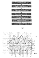
- Figure 1 a shows a typical lead frame structure 10 formed of a series of lead frame sub-structures.
- each of the six I/O terminals 12, 14 and 16 are electrically interconnected connected since they will be monolithically formed from a single piece of metal, typically by a photo etching process on sheet metal.
- I/O terminals 12, 14 will be detached from the leadframe structure 10, and therefore it will not be possible to electroplate the I/O terminals 12, 14 to form metal side pads because they will be mechanically detached and electrically isolated from the leadframe structure.
- each individual sub-lead frame will be singulated from the leadframe structure 10.
- a lead less packaged semiconductor device having a leadframe structure comprising an array leadframe sub-structures each having a semiconductor die arranged thereon, the method comprising: providing electrical connections between terminals of said lead frame sub-structures and said leadframe structure; encapsulating said leadframe structure, said electrical connections and said terminals in an encapsulation layer; performing a first series of parallel cuts extending through the leadframe structure and the encapsulation layer to expose a side portion of said terminals; electro-plating said terminals to form metal side pads; and performing a second series of parallel cuts angled with respect to the first series of parallel cuts, the second series of cuts extending through the lead frame structure and the encapsulation layer to singulate a semiconductor device from the leadframe structure.
- the electrical connections may be sacrificial bond wires, such that the electrical connections can be easily carried out whilst wire bonding the semiconductor dies.
- the sacrificial bond wires may each be provided between a terminal and a respective bond pad formed on said leadframe structure.
- the sacrificial bond wires are arranged to maintain electrical continuity between lead frame sub-structures following the first series of parallel cuts. Maintaining electrical continuity across an array of the lead frame sub-structures allows the metal side pads to be electroplated in a single step.
- the second series of cuts may sever the sacrificial bond wires between the terminals and the leadframe structure. This removes the electrical connection between terminals that are wire bonded to the semiconductor dies and the lead frame sub-structures, thereby preventing a risk of short circuiting the semiconductor dies.
- the leadframe structure may comprise at least five terminals and wherein at least two terminals may be disposed on one side of the leadframe structure and the remaining terminals may be disposed on an opposing side of the leadframe structure.
- the leadframe sub-structures may further comprise tie bars arranged to connect at least one of said terminals to said leadframe structure, whereby said tie bars are severed by the second series of cuts.
- the bars may provide mechanical support for the terminal on the lead frame structure.
- leadless packaged semiconductor device having top and bottom opposing major surfaces and sidewalls extending there between, the leadless packaged semiconductor device comprising; a lead frame structure comprising of an array of two or more leadframe sub-structures each having a semiconductor die arranged thereon; a sacrificial bond wire comprising a first end bonded to said lead frame structure and second end terminating in a side wall; and at least five terminals wherein each of said terminals comprise a respective metal side pad.
- the leadless packaged semiconductor device may therefore be amenable to optical inspection when mounted on a printed circuit board.
- the terminals may be disposed on opposing side walls, wherein at least two terminals are disposed on one of said sidewalls and the remaining terminals are disposed on an opposing side wall.
- Each of the leadframe sub-structures may comprise a die attach region comprising therewith an integrally formed terminal.
- Each of the two or more leadframe sub-structures may be electrically isolated.
- Each of metal side pads may be electroplated.
- a second end of said sacrificial bond wire may terminate in a sidewall adjacent sidewalls comprising the metal side pads.
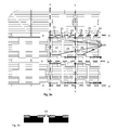
- the lead frame structure 20 known as a unit structure, according to an embodiment is illustrated in Figure 2 .
- the lead frame structure 20 is formed of a two-dimensional (2D) array of interconnected sub-structures each of which constitutes single lead frames 22, 28 for a leadless packaged semiconductor device when singulated.
- each of the lead frames comprises two sets of three I/O terminals 21, 23, 25, however the skilled person will appreciate that the number of I/O terminals may vary as required by the package type.
- Each of the lead frames 22, 28 also comprises at least two die attach regions 27 onto each of which a device die (not illustrated in Figure 2 ) may be attached, as discussed below.
- Each one of the two set of I/O terminals are associated with each one of the die attach regions 27 so that appropriate connections can be made to the device die.
- Applications requiring two dies include dual transistors arrangements such as cascode transistors or dual diodes.
- the die attach region 27 is integrally connected to I/O terminal 21 and in this regard the die attach region 27 will remain integrally connected to the I/O terminal 21 following the singulation process discussed below.
- each of the I/O terminals 23, 25 are integrally connected to the respective die attach region 27 my means of tie bars 29.
- the tie bars 29 connecting the die attach regions 27 to the I/O terminals 23, 25 are arranged to be broken during the singulation process, as discussed below.
- the I/O terminals are arranged such that they are formed along two parallel axes, known as the lead side axes, defining a row in the array.
- the lead frame structure is typically formed from a sheet of metal copper alloy coated with palladium gold by a photo etching process.
- FIG 3 illustrates a process flow diagram for fabricating a leadless packaged semiconductor device according to an embodiment.
- device dies 40 are attached to the die attach regions 27, by die bonding (process step 30).
- the device dies 40 may be attached to the die attach region by any appropriate means, such as eutectic bonds or glue adhesion between the die attach region 27 and a metallization of the device die 40.
- the metallization may be a backside metallization (not illustrated) of the device die 40. In this way a device die 40 is connected to a respective I/O terminal 21 both mechanically and electrically.
- wire bonds are connected from the contacts of the device dies 40 to the respective I/O terminals 23, 25 of the respective lead frames 22, 28.
- additional wire bonds 42 are connected between the I/O terminal 25, and additional bond pads 44 formed on the lead frame structure 20 (process step 34).
- the die wire bonding and the additional wire bonding may be performed in a simultaneous process step.
- the additional wire bonds 42 are arranged substantially parallel to a direction of first singulation cuts (discussed below at process step 36) made in the lead frame structure whereby these cuts are a first series of parallel cuts that extend fully through the leadframe to define separate rows of lead frames 22, 28 from the lead frame structure 20.
- the additional wire bonds 42 are also arranged such that they are not cut during the first singulation cuts, but remain to provide electrical continuity between each of the lead frames 22, 28 forming the rows following the first singulation cut. By providing electrical continuity in this way it is possible to carry electroplating of metal side pads for each of the I/O terminals 21, 23, 25 as discussed below (see step 38), for each of the respective lead frames 22, 24, 26, 28 making up the row.
- the wire bond processes discussed above may be any appropriate wire bonding process using gold copper, aluminium, or silver wire, or using metal clip bonds.
- the array of lead frames 22, 28 are encapsulated in a mould compound.
- the encapsulation defines a first set of opposing side walls for the leadless packaged semiconductor device. This encapsulation process may be any appropriate process as understood by the skilled person.
- a first series of parallel cuts are made in lead frame structure 20 (process step 36).
- the parallel series of cuts are singulation cuts, and are made along the path (X-X) following the line of the I/O terminals 21, 23, 25 so as to define separate rows of lead frames 22, 28.
- These first singulation cuts are such that the lead frames in a row of lead frames 22, 28 remain connected to the lead frame structure 20 at an end lead frame of a row and by connection to adjoining lead frames.
- the purpose of these cuts is to remove the encapsulation in the vicinity of the I/O terminals 21, 23, 25 so that they can be electroplated (in process step 38) as discussed below, to form metal side pads 54.
- Metal side pads 54 are illustrated in Figure 5b which shows a cross-section Y-Y taken from Figure 5a .
- the cuts are made in the direction X-X which follows the line of the I/O terminals 21, 23, 25 along the side lead axis.
- the cuts may extend through the encapsulation and the lead frame material but terminate at a tape material (not illustrated) such that each lead frame in a row remains mechanically connected to the tape.
- I/O terminals 25 of each lead frame 22, 28 in a row remain electrically connected to adjacent lead frames 22, 28 by means of the additional wire bonds 42.
- the lead frames will be wire bonded to a point on the lead frame structure 20 so as to create inter - lead frame connections.
- electroplating of the metal side pads 54 on each of the I/O terminals 21, 23, 25 is possible.
- tie bars 29 may be included to provide mechanical support for the I/O terminals 25, 23 on the lead frame structure 20.
- the tie bars 29 also provide electrical connection to the lead frame structure 20.
- the tie bars 29 are arranged to be severed, following electroplating, during a second series of parallel cuts (process step 39 discussed below) such that the I/O terminals 25, 23 do not short circuit to the die attach region 27.
- electroplating of the I/O terminals 21, 23, 25 is carried out so as to form the metal side pads 54.
- the electroplating can be achieved by any appropriate process as understood by those skilled in the art.
- the metal side pads 54 will be plated with tin or alternatively lead or a tin-lead compound.
- the electrical continuity necessary for electroplating the I/O terminals 21, 23, 25 of each lead frame 22, 28 in a row in a single step is achieved. In this way, the exposed metal of the I/O terminals 21, 23, 25 of each lead frame act as a plating electrode in the electroplating process.
- a second series of parallel cuts are made in lead frame structure 20 (process step 39).
- the second series of parallel cuts are final singulation cuts which completes the singulation process, and are made in a direction (Z-Z) at an angle to the first series of cuts and separate each of lead frames 22, 28 from the lead frame structure 20 and/or an adjacent lead frame 22, 28.
- These cuts define a second set of opposing side walls for each singulated device.
- the angle of the second series of cuts may be orthogonal to the first series.
- This final singulation step severs the additional wire bonds 42.
- the additional wire bonds 42 may be severed by cutting through the additional bond pads 44.
- the bond wire may be considered as sacrificial.
- the severed additional wire bonds 42 may remain embedded within the encapsulation but are functionally obsolete.
- the singulation step also severs the tie bars 29, such that the I/O terminals 25, 23 do not short circuit to the die attach region 27. Additionally, the I/O terminals will now not be mutually connected as a result of the final singulation.
- Additional processing steps may include deflashing, to remove any encapsulation compound from the I/O terminals, which may be performed before electroplating of the metal side pads. Further cleaning steps may be used to remove material from the final device following singulation. A visual inspection of the final may also be carried out.
- Figure 6a shows perspective underside view of a completed leadless semiconductor device according to an embodiment.
- the metal side pads 54 are formed on a side wall of the device from respective I/O terminals 21, 23, 25.
- metal side pads (obscured from view in Figure 6a ) are also provided on the opposing side wall of the device.
- a severed and now functionally obsolete additional bond wire 42 may be seen in an adjacent side wall of the device, that is sidewalls adjacent the sidewalls on which the metal side pads are formed.
- the additional bond wires 42 are severed at one end from the lead frame structure 20 such that they no longer provide electrical continuity as discussed above.
- the additional bond wire 42 may be obsolete in terms of device operation, they may provide electrical connections to the device for use in for example device testing or programming.
- I/O terminals and die attached regions need to be electrically connected to each other after the first cut, so as to allow for electroplating and then mutually electrically separated so as to allow for correct functioning of the device dies and ultimately the final packaged device.
Landscapes
- Lead Frames For Integrated Circuits (AREA)
Abstract
Description
- The present invention relates to a method of forming a leadless packaged semiconductor device. The invention also relates to a leadless packaged semiconductor device.
- Leadless packaged semiconductor devices are known to provide advantages over leaded packages. Those advantages include better electrical performance in terms of reduced lead inductance, good heat dissipation by use of an exposed thermal pad to improve heat transfer to a PCB (printed circuit board), reduced package thickness and smaller footprint, which reduces the area occupied on a PCB. Examples of leadless packaged semiconductor devices include QFN (quad-flat no-lead devices) and DFN (discrete-flat no-lead devices). However, a disadvantage of leadless packaged semiconductor devices is that inspection of solder joints when mounted on a PCB can be difficult. Conventional inspection techniques utilise so-called Automated Optical Inspection (AOI) systems, whereby a camera scans the leadless packaged semiconductor devices mounted on the PCB for a variety of defects such as open circuit connections, short circuit connections, thinning of the solder connections and incorrectly placed devices. Due to the semiconductor device I/O terminals being arranged on the bottom of the device, and therefore hidden from view when the device is mounted a PCB, it is not generally possible to use AOI systems with leadless semiconductor devices. Automatic XRay Inspection (AXI) systems may allow inspection of solder joints, however AXI systems are expensive.
- A solution allowing solder joints to be inspected by AOI is to include a metal side pads which extend from the device I/O terminals on the bottom of the device at least partially up external sidewall of the device. Typically the metal side pads may be formed of tin, lead or tin-lead alloys. During soldering processes attaching the device to the PCB, the solder will wet the I/O terminal on the bottom of the device and also the metal side pads. As a result a portion of the solder joint will be visible allowing inspection by AOI techniques. The solder joint may be considered good, provided that the metal side pads are correctly soldered even if the I/O terminal is not correctly soldered to the PCB.
- In addition to ease of inspection, metal side pads may reduce tilting of the device when mounted on a PCB. Metal side pads may also improve shearing and bending performance because of the increased soldered area.
- Typically, a package structure will comprise an array of device dies embedded in an encapsulation layer. The device dies will be connected to a leadframe by any appropriate means, such as eutectic bonds. The process of forming a such leadless device involves dividing a two dimensional array of encapsulated integrated circuits into individual semiconductor device packages using a series of parallel row cuts and parallel column cuts. The first series of parallel cuts extend fully through the leadframe and encapsulation layer defining rows of the array.
- After electro-plating metal side pads, a second series of parallel cuts is made extending fully through the leadframe and encapsulation layer. This separates the columns of the array thereby providing singulated packages. In such a process the I/O terminals will be exposed and since the I/O terminals are mutually electrically connected the exposed I/O terminals may be electroplated to form the metal side pads. The electrical connection is necessary to maintain electrical continuity so that the electroplating process can be achieved.
- However, for leadless semiconductor devices having two separate functional dies and at least three I/O terminals located at one sidewall of the device and at least two I/O terminals located at an opposing sidewall, it may not be possible to form side pads by electroplating according to above process because the cutting sequence requires that middle I/O terminals located at one sidewall of the device formed on a leadframe structure on lead frame will be electrically isolated.
Figure 1 a shows a typicallead frame structure 10 formed of a series of lead frame sub-structures. - Prior to the first cutting sequence to define rows, as discussed above, each of the six I/
O terminals Figure 1b , following the first cutting sequence (indicated by lines A) I/O terminals leadframe structure 10, and therefore it will not be possible to electroplate the I/O terminals - Following the second cutting sequence which is substantially orthogonal to the first cutting sequence, (indicated by lines B) each individual sub-lead frame will be singulated from the
leadframe structure 10. - According to a first aspect there is provided method of forming a lead less packaged semiconductor device having a leadframe structure comprising an array leadframe sub-structures each having a semiconductor die arranged thereon, the method comprising: providing electrical connections between terminals of said lead frame sub-structures and said leadframe structure; encapsulating said leadframe structure, said electrical connections and said terminals in an encapsulation layer; performing a first series of parallel cuts extending through the leadframe structure and the encapsulation layer to expose a side portion of said terminals; electro-plating said terminals to form metal side pads; and performing a second series of parallel cuts angled with respect to the first series of parallel cuts, the second series of cuts extending through the lead frame structure and the encapsulation layer to singulate a semiconductor device from the leadframe structure.
- Use of the electrical connections between terminals of the lead frame sub-structures and the leadframe structure allows for electroplating of the metal side pads.
- The electrical connections may be sacrificial bond wires, such that the electrical connections can be easily carried out whilst wire bonding the semiconductor dies.
- The sacrificial bond wires may each be provided between a terminal and a respective bond pad formed on said leadframe structure. The sacrificial bond wires are arranged to maintain electrical continuity between lead frame sub-structures following the first series of parallel cuts. Maintaining electrical continuity across an array of the lead frame sub-structures allows the metal side pads to be electroplated in a single step.
- The second series of cuts may sever the sacrificial bond wires between the terminals and the leadframe structure. This removes the electrical connection between terminals that are wire bonded to the semiconductor dies and the lead frame sub-structures, thereby preventing a risk of short circuiting the semiconductor dies.
- The leadframe structure may comprise at least five terminals and wherein at least two terminals may be disposed on one side of the leadframe structure and the remaining terminals may be disposed on an opposing side of the leadframe structure.
- The leadframe sub-structures may further comprise tie bars arranged to connect at least one of said terminals to said leadframe structure, whereby said tie bars are severed by the second series of cuts. The bars may provide mechanical support for the terminal on the lead frame structure.
- According to a second aspect there is provided leadless packaged semiconductor device having top and bottom opposing major surfaces and sidewalls extending there between, the leadless packaged semiconductor device comprising; a lead frame structure comprising of an array of two or more leadframe sub-structures each having a semiconductor die arranged thereon; a sacrificial bond wire comprising a first end bonded to said lead frame structure and second end terminating in a side wall; and at least five terminals wherein each of said terminals comprise a respective metal side pad.
- The leadless packaged semiconductor device may therefore be amenable to optical inspection when mounted on a printed circuit board.
- The terminals may be disposed on opposing side walls, wherein at least two terminals are disposed on one of said sidewalls and the remaining terminals are disposed on an opposing side wall.
- Each of the leadframe sub-structures may comprise a die attach region comprising therewith an integrally formed terminal. Each of the two or more leadframe sub-structures may be electrically isolated. Each of metal side pads may be electroplated. A second end of said sacrificial bond wire may terminate in a sidewall adjacent sidewalls comprising the metal side pads.
- The invention is described further hereinafter by way of example only with reference to the accompanying drawings in which:
-
Figure 1 a shows a known lead frame structure; -
Figure 1b shows a known lead frame structure indicating the location of singulation cuts; -
Figure 2 illustrates a lead frame structure according to embodiments; -
Figure 3 illustrates a process flow for forming a leadless semiconductor device according to embodiments; -
Figure 4 illustrates a wire bonding scheme according to embodiments; -
Figure 5a illustrates a lead frame structure and wire bonding scheme according to embodiments following partial singulation; -
Figure 5b illustrates a cross-section y-y ofFigure 5a ; -
Figure 5c illustrates a lead frame structure and wire bonding scheme according to embodiments following singulation; -
Figure 6a illustrates an underside view of completed leadless semiconductor device according to embodiments; and -
Figure 6b illustrates a cut-away view of the completed leadless semiconductor device. - In the figures and the following description like reference numerals refer to like features.
- In overview, the
lead frame structure 20, known as a unit structure, according to an embodiment is illustrated inFigure 2 . Thelead frame structure 20 is formed of a two-dimensional (2D) array of interconnected sub-structures each of which constitutes single lead frames 22, 28 for a leadless packaged semiconductor device when singulated. In this example, each of the lead frames comprises two sets of three I/O terminals regions 27 onto each of which a device die (not illustrated inFigure 2 ) may be attached, as discussed below. Each one of the two set of I/O terminals are associated with each one of the die attachregions 27 so that appropriate connections can be made to the device die. Applications requiring two dies include dual transistors arrangements such as cascode transistors or dual diodes. - The die attach
region 27 is integrally connected to I/O terminal 21 and in this regard the die attachregion 27 will remain integrally connected to the I/O terminal 21 following the singulation process discussed below. Prior to singulation each of the I/O terminals region 27 my means of tie bars 29. The tie bars 29 connecting the die attachregions 27 to the I/O terminals - The lead frame structure is typically formed from a sheet of metal copper alloy coated with palladium gold by a photo etching process.
-
Figure 3 illustrates a process flow diagram for fabricating a leadless packaged semiconductor device according to an embodiment. With reference to the process flow ofFigure 3 and the wire bonding scheme ofFigure 4 , following formation of thelead frame structure 20 as discussed above, device dies 40 are attached to the die attachregions 27, by die bonding (process step 30). The device dies 40 may be attached to the die attach region by any appropriate means, such as eutectic bonds or glue adhesion between the die attachregion 27 and a metallization of the device die 40. For example the metallization may be a backside metallization (not illustrated) of the device die 40. In this way a device die 40 is connected to a respective I/O terminal 21 both mechanically and electrically. - Also with reference to
Figure 4 , following thedie bonding step 30, wire bonds (process step 32) are connected from the contacts of the device dies 40 to the respective I/O terminals O terminals additional wire bonds 42 are connected between the I/O terminal 25, andadditional bond pads 44 formed on the lead frame structure 20 (process step 34). The die wire bonding and the additional wire bonding may be performed in a simultaneous process step. Theadditional wire bonds 42 are arranged substantially parallel to a direction of first singulation cuts (discussed below at process step 36) made in the lead frame structure whereby these cuts are a first series of parallel cuts that extend fully through the leadframe to define separate rows of lead frames 22, 28 from thelead frame structure 20. Theadditional wire bonds 42 are also arranged such that they are not cut during the first singulation cuts, but remain to provide electrical continuity between each of the lead frames 22, 28 forming the rows following the first singulation cut. By providing electrical continuity in this way it is possible to carry electroplating of metal side pads for each of the I/O terminals - Following the wire bonding (process steps 32 and 34), the array of lead frames 22, 28 are encapsulated in a mould compound. The encapsulation defines a first set of opposing side walls for the leadless packaged semiconductor device. This encapsulation process may be any appropriate process as understood by the skilled person.
- Following encapsulation, a first series of parallel cuts (as discussed above) are made in lead frame structure 20 (process step 36). With reference to
Figure 5a , the parallel series of cuts are singulation cuts, and are made along the path (X-X) following the line of the I/O terminals lead frame structure 20 at an end lead frame of a row and by connection to adjoining lead frames. The purpose of these cuts is to remove the encapsulation in the vicinity of the I/O terminals metal side pads 54.Metal side pads 54 are illustrated inFigure 5b which shows a cross-section Y-Y taken fromFigure 5a . The cuts are made in the direction X-X which follows the line of the I/O terminals Figure 5a , it can be seen that I/O terminals 25 of eachlead frame lead frame structure 20 so as to create inter - lead frame connections. By making these connections electroplating of themetal side pads 54 on each of the I/O terminals Figure 5a , tie bars 29 may be included to provide mechanical support for the I/O terminals lead frame structure 20. The tie bars 29 also provide electrical connection to thelead frame structure 20. The tie bars 29 are arranged to be severed, following electroplating, during a second series of parallel cuts (process step 39 discussed below) such that the I/O terminals region 27. - Following the first series of cuts, electroplating (process step 38) of the I/
O terminals metal side pads 54. The electroplating can be achieved by any appropriate process as understood by those skilled in the art. Typically, themetal side pads 54 will be plated with tin or alternatively lead or a tin-lead compound. Through use of theadditional wire bonds 42 the electrical continuity necessary for electroplating the I/O terminals lead frame O terminals - Following the electroplating step, a second series of parallel cuts (as discussed above) are made in lead frame structure 20 (process step 39). With reference to
Figure 5c the second series of parallel cuts are final singulation cuts which completes the singulation process, and are made in a direction (Z-Z) at an angle to the first series of cuts and separate each of lead frames 22, 28 from thelead frame structure 20 and/or anadjacent lead frame - This final singulation step severs the additional wire bonds 42. The
additional wire bonds 42 may be severed by cutting through theadditional bond pads 44. In this regard the bond wire may be considered as sacrificial. The severedadditional wire bonds 42 may remain embedded within the encapsulation but are functionally obsolete. The singulation step also severs the tie bars 29, such that the I/O terminals region 27. Additionally, the I/O terminals will now not be mutually connected as a result of the final singulation. - Additional processing steps may include deflashing, to remove any encapsulation compound from the I/O terminals, which may be performed before electroplating of the metal side pads. Further cleaning steps may be used to remove material from the final device following singulation. A visual inspection of the final may also be carried out.
-
Figure 6a shows perspective underside view of a completed leadless semiconductor device according to an embodiment. Themetal side pads 54 are formed on a side wall of the device from respective I/O terminals Figure 6a ) are also provided on the opposing side wall of the device. A severed and now functionally obsoleteadditional bond wire 42 may be seen in an adjacent side wall of the device, that is sidewalls adjacent the sidewalls on which the metal side pads are formed. As shown inFigure 6b theadditional bond wires 42 are severed at one end from thelead frame structure 20 such that they no longer provide electrical continuity as discussed above. - Whilst the skilled person will appreciate that the
additional bond wire 42 may be obsolete in terms of device operation, they may provide electrical connections to the device for use in for example device testing or programming. - Whilst the above discussion relates to leadless packaged semiconductor devices having three or more I/O terminals on each opposing side of the device (that is arranged as a so-called dual in line arrangement), and with two or more electrically isolated die attach
regions 27, the process can be used for multiple I/O terminal configurations and multiple electrically isolated die attached regions. The skilled person will appreciate that I/O terminals and die attached regions need to be electrically connected to each other after the first cut, so as to allow for electroplating and then mutually electrically separated so as to allow for correct functioning of the device dies and ultimately the final packaged device. - Particular and preferred aspects of the invention are set out in the accompanying independent claims. Combinations of features from the dependent and/or independent claims may be combined as appropriate and not merely as set out in the claims.
- The scope of the present disclosure includes any novel feature or combination of features disclosed therein either explicitly or implicitly or any generalisation thereof irrespective of whether or not it relates to the claimed invention or mitigate against any or all of the problems addressed by the present invention. The applicant hereby gives notice that new claims may be formulated to such features during prosecution of this application or of any such further application derived there from. In particular, with reference to the appended claims, features from dependent claims may be combined with those of the independent claims and features from respective independent claims may be combined in any appropriate manner and not merely in specific combinations enumerated in the claims.
- Features which are described in the context of separate embodiments may also be provided in combination in a single embodiment. Conversely, various features which are, for brevity, described in the context of a single embodiment, may also be provided separately or in any suitable sub combination.
- Term "comprising" does not exclude other elements or steps, the term "a" or "an" does not exclude a plurality. Reference signs in the claims shall not be construed as limiting the scope of the claims.
Claims (13)
- A method of forming a leadless packaged semiconductor device having a leadframe structure comprising an array leadframe sub-structures each having a semiconductor die arranged thereon, the method comprising:providing electrical connections between terminals of said lead frame sub-structures and said leadframe structure;encapsulating said leadframe structure, said electrical connections and said terminals in an encapsulation layer;performing a first series of parallel cuts extending through the leadframe structure and the encapsulation layer to expose a side portion of said terminals;electro-plating said terminals to form metal side pads; andperforming a second series of parallel cuts angled with respect to the first series of parallel cuts, the second series of cuts extending through the lead frame structure and the encapsulation layer to singulate a semiconductor device from the leadframe structure.
- The method of claim 1, wherein said electrical connections are sacrificial bond wires.
- The method of claim 2, wherein said sacrificial bond wires are each provided between a terminal of a leadframe sub-structure and a respective bond pad formed on said leadframe structure.
- The method of claim 3, wherein said sacrificial bond wires are arranged to maintain electrical continuity between lead frame sub-structures following the first series of parallel cuts.
- The method of claims 2 to 4, wherein performing the second series of cuts sever the sacrificial bond wires between said terminals and the leadframe structure.
- The method of any preceding claim, wherein leadframe structure comprises at least five terminals and wherein at least two terminals are disposed on one side of a leadframe sub-structure and the remaining terminals are on an opposing side of leadframe sub-structure.
- The method of any preceding claim, wherein said leadframe sub-structures further comprise tie bars arranged to connect at least one of said terminals to said leadframe structure, whereby said tie bars are severed by the second series of cuts.
- A leadless packaged semiconductor device having top and bottom opposing major surfaces and sidewalls extending there between, the leadless packaged semiconductor device comprising;
a lead frame structure comprising of an array of two or more leadframe sub-structures each having a semiconductor die arranged thereon;
a sacrificial bond wire comprising a first end bonded to said lead frame structure and second end terminating in a side wall; and
at least five terminals wherein each of said terminals comprise a respective metal side pad. - The leadless packaged semiconductor device of claim 8, wherein the terminals are disposed on opposing side walls, wherein at least two terminals are disposed on one of said sidewalls and the remaining terminals are disposed on an opposing side wall.
- The leadless packaged semiconductor device of claims 8 or 9, wherein each of the leadframe sub-structures comprise a die attach region comprising therewith an integrally formed terminal.
- The leadless packaged semiconductor device of any preceding claim, wherein each of two or more leadframe sub-structures are electrically isolated.
- The leadless packaged semiconductor device of claim 9, wherein each of metal side pads are electroplated.
- The leadless packaged semiconductor device of claim 9, wherein the second end of said sacrificial bond wire terminates in a sidewall adjacent sidewalls comprising the metal side pads.
Priority Applications (3)
| Application Number | Priority Date | Filing Date | Title |
|---|---|---|---|
| EP14179517.9A EP2980845B1 (en) | 2014-08-01 | 2014-08-01 | A leadless semiconductor package and method |
| US14/801,635 US9443791B2 (en) | 2014-08-01 | 2015-07-16 | Leadless semiconductor package and method |
| CN201510454935.1A CN105321919B (en) | 2014-08-01 | 2015-07-29 | No lead semiconductor encapsulation and method |
Applications Claiming Priority (1)
| Application Number | Priority Date | Filing Date | Title |
|---|---|---|---|
| EP14179517.9A EP2980845B1 (en) | 2014-08-01 | 2014-08-01 | A leadless semiconductor package and method |
Publications (2)
| Publication Number | Publication Date |
|---|---|
| EP2980845A1 true EP2980845A1 (en) | 2016-02-03 |
| EP2980845B1 EP2980845B1 (en) | 2019-11-27 |
Family
ID=51257423
Family Applications (1)
| Application Number | Title | Priority Date | Filing Date |
|---|---|---|---|
| EP14179517.9A Active EP2980845B1 (en) | 2014-08-01 | 2014-08-01 | A leadless semiconductor package and method |
Country Status (2)
| Country | Link |
|---|---|
| US (1) | US9443791B2 (en) |
| EP (1) | EP2980845B1 (en) |
Cited By (2)
| Publication number | Priority date | Publication date | Assignee | Title |
|---|---|---|---|---|
| US10431560B2 (en) | 2016-03-03 | 2019-10-01 | Infineon Technologies Ag | Molded semiconductor package having an optical inspection feature |
| EP3879569A1 (en) * | 2020-03-11 | 2021-09-15 | Nexperia B.V. | A leadless semiconductor package and method of manufacture |
Families Citing this family (8)
| Publication number | Priority date | Publication date | Assignee | Title |
|---|---|---|---|---|
| US9373569B1 (en) | 2015-09-01 | 2016-06-21 | Texas Instruments Incorporation | Flat no-lead packages with electroplated edges |
| JP7043508B2 (en) | 2017-03-03 | 2022-03-29 | ヒタチ・エナジー・スウィツァーランド・アクチェンゲゼルシャフト | Power module interconnect member |
| US12224232B2 (en) | 2019-03-08 | 2025-02-11 | Siliconix Incorporated | Semiconductor package having side wall plating |
| EP3935663A4 (en) | 2019-03-08 | 2022-11-02 | Siliconix Incorporated | SEMICONDUCTOR PACKAGE HAVING SIDE WALL PLATING |
| CN113035721A (en) | 2019-12-24 | 2021-06-25 | 维谢综合半导体有限责任公司 | Packaging process for plating conductive film on side wall |
| CN113035722A (en) | 2019-12-24 | 2021-06-25 | 维谢综合半导体有限责任公司 | Packaging process for plating with selective molding |
| EP4040470A1 (en) * | 2021-02-03 | 2022-08-10 | Nexperia B.V. | A semiconductor device and a method of manufacturing a semiconductor device |
| EP4531078A1 (en) | 2023-09-26 | 2025-04-02 | Nexperia B.V. | Method of and intermediate for manufacturing a semiconductor die package |
Citations (5)
| Publication number | Priority date | Publication date | Assignee | Title |
|---|---|---|---|---|
| US20100187663A1 (en) * | 2009-01-29 | 2010-07-29 | Phillip Celaya | Method for manufacturing a semiconductor component and structure therefor |
| US8076181B1 (en) * | 2010-10-22 | 2011-12-13 | Linear Technology Corporation | Lead plating technique for singulated IC packages |
| WO2012040873A1 (en) * | 2010-09-29 | 2012-04-05 | Nxp B.V. | Singulation of ic packages |
| US20140035113A1 (en) * | 2012-08-01 | 2014-02-06 | Analog Devices, Inc. | Packaging and methods for packaging |
| US20140042599A1 (en) * | 2012-08-13 | 2014-02-13 | Chung-Lin Wu | Multi-chip module power clip |
Family Cites Families (2)
| Publication number | Priority date | Publication date | Assignee | Title |
|---|---|---|---|---|
| US7169651B2 (en) * | 2004-08-11 | 2007-01-30 | Advanced Semiconductor Engineering, Inc. | Process and lead frame for making leadless semiconductor packages |
| CN102789994B (en) * | 2011-05-18 | 2016-08-10 | 飞思卡尔半导体公司 | The wettable semiconductor device in side |
-
2014
- 2014-08-01 EP EP14179517.9A patent/EP2980845B1/en active Active
-
2015
- 2015-07-16 US US14/801,635 patent/US9443791B2/en active Active
Patent Citations (5)
| Publication number | Priority date | Publication date | Assignee | Title |
|---|---|---|---|---|
| US20100187663A1 (en) * | 2009-01-29 | 2010-07-29 | Phillip Celaya | Method for manufacturing a semiconductor component and structure therefor |
| WO2012040873A1 (en) * | 2010-09-29 | 2012-04-05 | Nxp B.V. | Singulation of ic packages |
| US8076181B1 (en) * | 2010-10-22 | 2011-12-13 | Linear Technology Corporation | Lead plating technique for singulated IC packages |
| US20140035113A1 (en) * | 2012-08-01 | 2014-02-06 | Analog Devices, Inc. | Packaging and methods for packaging |
| US20140042599A1 (en) * | 2012-08-13 | 2014-02-13 | Chung-Lin Wu | Multi-chip module power clip |
Cited By (5)
| Publication number | Priority date | Publication date | Assignee | Title |
|---|---|---|---|---|
| US10431560B2 (en) | 2016-03-03 | 2019-10-01 | Infineon Technologies Ag | Molded semiconductor package having an optical inspection feature |
| DE102017104430B4 (en) | 2016-03-03 | 2020-07-02 | Infineon Technologies Ag | Method for producing molded semiconductor packages comprising an optical inspection feature and molded semiconductor package |
| DE102017012329B3 (en) | 2016-03-03 | 2024-09-12 | Infineon Technologies Ag | Method for producing molded semiconductor packages having an optical inspection feature |
| EP3879569A1 (en) * | 2020-03-11 | 2021-09-15 | Nexperia B.V. | A leadless semiconductor package and method of manufacture |
| US11631634B2 (en) | 2020-03-11 | 2023-04-18 | Nexperia B.V. | Leadless semiconductor package and method of manufacture |
Also Published As
| Publication number | Publication date |
|---|---|
| CN105321919A (en) | 2016-02-10 |
| US9443791B2 (en) | 2016-09-13 |
| EP2980845B1 (en) | 2019-11-27 |
| US20160035651A1 (en) | 2016-02-04 |
Similar Documents
| Publication | Publication Date | Title |
|---|---|---|
| US9443791B2 (en) | Leadless semiconductor package and method | |
| US11342252B2 (en) | Leadframe leads having fully plated end faces | |
| US9177836B1 (en) | Packaged integrated circuit device having bent leads | |
| TWI833739B (en) | Semiconductor package and method for fabricating the same | |
| TWI587457B (en) | Resin sealed type semiconductor device and method of manufacturing same | |
| US8076181B1 (en) | Lead plating technique for singulated IC packages | |
| US9363901B2 (en) | Making a plurality of integrated circuit packages | |
| US20160126169A1 (en) | Leadless semiconductor device and method of making thereof | |
| CN107112305A (en) | Flat No Lead package with improved contact pin | |
| US12119263B2 (en) | Methods and apparatus for an improved integrated circuit package | |
| US11227820B2 (en) | Through hole side wettable flank | |
| US11631634B2 (en) | Leadless semiconductor package and method of manufacture | |
| US20220246505A1 (en) | Semiconductor device and a method of manufacturing a semiconductor device | |
| US11728179B2 (en) | Surface mount semiconductor device and method of manufacture | |
| US20200321228A1 (en) | Method of manufacturing a lead frame, method of manufacturing an electronic apparatus, and electronic apparatus | |
| CN105321919B (en) | No lead semiconductor encapsulation and method | |
| HK40063596A (en) | Semiconductor package having side wall plating |
Legal Events
| Date | Code | Title | Description |
|---|---|---|---|
| PUAI | Public reference made under article 153(3) epc to a published international application that has entered the european phase |
Free format text: ORIGINAL CODE: 0009012 |
|
| AK | Designated contracting states |
Kind code of ref document: A1 Designated state(s): AL AT BE BG CH CY CZ DE DK EE ES FI FR GB GR HR HU IE IS IT LI LT LU LV MC MK MT NL NO PL PT RO RS SE SI SK SM TR |
|
| AX | Request for extension of the european patent |
Extension state: BA ME |
|
| 17P | Request for examination filed |
Effective date: 20160803 |
|
| RBV | Designated contracting states (corrected) |
Designated state(s): AL AT BE BG CH CY CZ DE DK EE ES FI FR GB GR HR HU IE IS IT LI LT LU LV MC MK MT NL NO PL PT RO RS SE SI SK SM TR |
|
| RAP1 | Party data changed (applicant data changed or rights of an application transferred) |
Owner name: NEXPERIA B.V. |
|
| STAA | Information on the status of an ep patent application or granted ep patent |
Free format text: STATUS: EXAMINATION IS IN PROGRESS |
|
| 17Q | First examination report despatched |
Effective date: 20170202 |
|
| RAP1 | Party data changed (applicant data changed or rights of an application transferred) |
Owner name: NEXPERIA B.V. |
|
| GRAP | Despatch of communication of intention to grant a patent |
Free format text: ORIGINAL CODE: EPIDOSNIGR1 |
|
| STAA | Information on the status of an ep patent application or granted ep patent |
Free format text: STATUS: GRANT OF PATENT IS INTENDED |
|
| INTG | Intention to grant announced |
Effective date: 20190726 |
|
| GRAS | Grant fee paid |
Free format text: ORIGINAL CODE: EPIDOSNIGR3 |
|
| GRAA | (expected) grant |
Free format text: ORIGINAL CODE: 0009210 |
|
| STAA | Information on the status of an ep patent application or granted ep patent |
Free format text: STATUS: THE PATENT HAS BEEN GRANTED |
|
| AK | Designated contracting states |
Kind code of ref document: B1 Designated state(s): AL AT BE BG CH CY CZ DE DK EE ES FI FR GB GR HR HU IE IS IT LI LT LU LV MC MK MT NL NO PL PT RO RS SE SI SK SM TR |
|
| REG | Reference to a national code |
Ref country code: GB Ref legal event code: FG4D |
|
| REG | Reference to a national code |
Ref country code: CH Ref legal event code: EP |
|
| REG | Reference to a national code |
Ref country code: AT Ref legal event code: REF Ref document number: 1207669 Country of ref document: AT Kind code of ref document: T Effective date: 20191215 |
|
| REG | Reference to a national code |
Ref country code: DE Ref legal event code: R096 Ref document number: 602014057396 Country of ref document: DE |
|
| REG | Reference to a national code |
Ref country code: IE Ref legal event code: FG4D |
|
| REG | Reference to a national code |
Ref country code: NL Ref legal event code: MP Effective date: 20191127 |
|
| REG | Reference to a national code |
Ref country code: LT Ref legal event code: MG4D |
|
| PG25 | Lapsed in a contracting state [announced via postgrant information from national office to epo] |
Ref country code: NL Free format text: LAPSE BECAUSE OF FAILURE TO SUBMIT A TRANSLATION OF THE DESCRIPTION OR TO PAY THE FEE WITHIN THE PRESCRIBED TIME-LIMIT Effective date: 20191127 Ref country code: SE Free format text: LAPSE BECAUSE OF FAILURE TO SUBMIT A TRANSLATION OF THE DESCRIPTION OR TO PAY THE FEE WITHIN THE PRESCRIBED TIME-LIMIT Effective date: 20191127 Ref country code: LV Free format text: LAPSE BECAUSE OF FAILURE TO SUBMIT A TRANSLATION OF THE DESCRIPTION OR TO PAY THE FEE WITHIN THE PRESCRIBED TIME-LIMIT Effective date: 20191127 Ref country code: BG Free format text: LAPSE BECAUSE OF FAILURE TO SUBMIT A TRANSLATION OF THE DESCRIPTION OR TO PAY THE FEE WITHIN THE PRESCRIBED TIME-LIMIT Effective date: 20200227 Ref country code: FI Free format text: LAPSE BECAUSE OF FAILURE TO SUBMIT A TRANSLATION OF THE DESCRIPTION OR TO PAY THE FEE WITHIN THE PRESCRIBED TIME-LIMIT Effective date: 20191127 Ref country code: NO Free format text: LAPSE BECAUSE OF FAILURE TO SUBMIT A TRANSLATION OF THE DESCRIPTION OR TO PAY THE FEE WITHIN THE PRESCRIBED TIME-LIMIT Effective date: 20200227 Ref country code: LT Free format text: LAPSE BECAUSE OF FAILURE TO SUBMIT A TRANSLATION OF THE DESCRIPTION OR TO PAY THE FEE WITHIN THE PRESCRIBED TIME-LIMIT Effective date: 20191127 Ref country code: GR Free format text: LAPSE BECAUSE OF FAILURE TO SUBMIT A TRANSLATION OF THE DESCRIPTION OR TO PAY THE FEE WITHIN THE PRESCRIBED TIME-LIMIT Effective date: 20200228 |
|
| PG25 | Lapsed in a contracting state [announced via postgrant information from national office to epo] |
Ref country code: RS Free format text: LAPSE BECAUSE OF FAILURE TO SUBMIT A TRANSLATION OF THE DESCRIPTION OR TO PAY THE FEE WITHIN THE PRESCRIBED TIME-LIMIT Effective date: 20191127 Ref country code: IS Free format text: LAPSE BECAUSE OF FAILURE TO SUBMIT A TRANSLATION OF THE DESCRIPTION OR TO PAY THE FEE WITHIN THE PRESCRIBED TIME-LIMIT Effective date: 20200327 Ref country code: HR Free format text: LAPSE BECAUSE OF FAILURE TO SUBMIT A TRANSLATION OF THE DESCRIPTION OR TO PAY THE FEE WITHIN THE PRESCRIBED TIME-LIMIT Effective date: 20191127 |
|
| PG25 | Lapsed in a contracting state [announced via postgrant information from national office to epo] |
Ref country code: AL Free format text: LAPSE BECAUSE OF FAILURE TO SUBMIT A TRANSLATION OF THE DESCRIPTION OR TO PAY THE FEE WITHIN THE PRESCRIBED TIME-LIMIT Effective date: 20191127 |
|
| PG25 | Lapsed in a contracting state [announced via postgrant information from national office to epo] |
Ref country code: ES Free format text: LAPSE BECAUSE OF FAILURE TO SUBMIT A TRANSLATION OF THE DESCRIPTION OR TO PAY THE FEE WITHIN THE PRESCRIBED TIME-LIMIT Effective date: 20191127 Ref country code: RO Free format text: LAPSE BECAUSE OF FAILURE TO SUBMIT A TRANSLATION OF THE DESCRIPTION OR TO PAY THE FEE WITHIN THE PRESCRIBED TIME-LIMIT Effective date: 20191127 Ref country code: CZ Free format text: LAPSE BECAUSE OF FAILURE TO SUBMIT A TRANSLATION OF THE DESCRIPTION OR TO PAY THE FEE WITHIN THE PRESCRIBED TIME-LIMIT Effective date: 20191127 Ref country code: DK Free format text: LAPSE BECAUSE OF FAILURE TO SUBMIT A TRANSLATION OF THE DESCRIPTION OR TO PAY THE FEE WITHIN THE PRESCRIBED TIME-LIMIT Effective date: 20191127 Ref country code: PT Free format text: LAPSE BECAUSE OF FAILURE TO SUBMIT A TRANSLATION OF THE DESCRIPTION OR TO PAY THE FEE WITHIN THE PRESCRIBED TIME-LIMIT Effective date: 20200419 Ref country code: EE Free format text: LAPSE BECAUSE OF FAILURE TO SUBMIT A TRANSLATION OF THE DESCRIPTION OR TO PAY THE FEE WITHIN THE PRESCRIBED TIME-LIMIT Effective date: 20191127 |
|
| REG | Reference to a national code |
Ref country code: DE Ref legal event code: R097 Ref document number: 602014057396 Country of ref document: DE |
|
| PG25 | Lapsed in a contracting state [announced via postgrant information from national office to epo] |
Ref country code: SM Free format text: LAPSE BECAUSE OF FAILURE TO SUBMIT A TRANSLATION OF THE DESCRIPTION OR TO PAY THE FEE WITHIN THE PRESCRIBED TIME-LIMIT Effective date: 20191127 Ref country code: SK Free format text: LAPSE BECAUSE OF FAILURE TO SUBMIT A TRANSLATION OF THE DESCRIPTION OR TO PAY THE FEE WITHIN THE PRESCRIBED TIME-LIMIT Effective date: 20191127 |
|
| REG | Reference to a national code |
Ref country code: AT Ref legal event code: MK05 Ref document number: 1207669 Country of ref document: AT Kind code of ref document: T Effective date: 20191127 |
|
| PLBE | No opposition filed within time limit |
Free format text: ORIGINAL CODE: 0009261 |
|
| STAA | Information on the status of an ep patent application or granted ep patent |
Free format text: STATUS: NO OPPOSITION FILED WITHIN TIME LIMIT |
|
| 26N | No opposition filed |
Effective date: 20200828 |
|
| PG25 | Lapsed in a contracting state [announced via postgrant information from national office to epo] |
Ref country code: AT Free format text: LAPSE BECAUSE OF FAILURE TO SUBMIT A TRANSLATION OF THE DESCRIPTION OR TO PAY THE FEE WITHIN THE PRESCRIBED TIME-LIMIT Effective date: 20191127 Ref country code: SI Free format text: LAPSE BECAUSE OF FAILURE TO SUBMIT A TRANSLATION OF THE DESCRIPTION OR TO PAY THE FEE WITHIN THE PRESCRIBED TIME-LIMIT Effective date: 20191127 Ref country code: PL Free format text: LAPSE BECAUSE OF FAILURE TO SUBMIT A TRANSLATION OF THE DESCRIPTION OR TO PAY THE FEE WITHIN THE PRESCRIBED TIME-LIMIT Effective date: 20191127 |
|
| PG25 | Lapsed in a contracting state [announced via postgrant information from national office to epo] |
Ref country code: IT Free format text: LAPSE BECAUSE OF FAILURE TO SUBMIT A TRANSLATION OF THE DESCRIPTION OR TO PAY THE FEE WITHIN THE PRESCRIBED TIME-LIMIT Effective date: 20191127 |
|
| PG25 | Lapsed in a contracting state [announced via postgrant information from national office to epo] |
Ref country code: MC Free format text: LAPSE BECAUSE OF FAILURE TO SUBMIT A TRANSLATION OF THE DESCRIPTION OR TO PAY THE FEE WITHIN THE PRESCRIBED TIME-LIMIT Effective date: 20191127 |
|
| REG | Reference to a national code |
Ref country code: CH Ref legal event code: PL |
|
| GBPC | Gb: european patent ceased through non-payment of renewal fee |
Effective date: 20200801 |
|
| PG25 | Lapsed in a contracting state [announced via postgrant information from national office to epo] |
Ref country code: LU Free format text: LAPSE BECAUSE OF NON-PAYMENT OF DUE FEES Effective date: 20200801 Ref country code: LI Free format text: LAPSE BECAUSE OF NON-PAYMENT OF DUE FEES Effective date: 20200831 Ref country code: CH Free format text: LAPSE BECAUSE OF NON-PAYMENT OF DUE FEES Effective date: 20200831 |
|
| REG | Reference to a national code |
Ref country code: BE Ref legal event code: MM Effective date: 20200831 |
|
| PG25 | Lapsed in a contracting state [announced via postgrant information from national office to epo] |
Ref country code: FR Free format text: LAPSE BECAUSE OF NON-PAYMENT OF DUE FEES Effective date: 20200831 |
|
| PG25 | Lapsed in a contracting state [announced via postgrant information from national office to epo] |
Ref country code: BE Free format text: LAPSE BECAUSE OF NON-PAYMENT OF DUE FEES Effective date: 20200831 Ref country code: GB Free format text: LAPSE BECAUSE OF NON-PAYMENT OF DUE FEES Effective date: 20200801 Ref country code: IE Free format text: LAPSE BECAUSE OF NON-PAYMENT OF DUE FEES Effective date: 20200801 |
|
| PG25 | Lapsed in a contracting state [announced via postgrant information from national office to epo] |
Ref country code: TR Free format text: LAPSE BECAUSE OF FAILURE TO SUBMIT A TRANSLATION OF THE DESCRIPTION OR TO PAY THE FEE WITHIN THE PRESCRIBED TIME-LIMIT Effective date: 20191127 Ref country code: MT Free format text: LAPSE BECAUSE OF FAILURE TO SUBMIT A TRANSLATION OF THE DESCRIPTION OR TO PAY THE FEE WITHIN THE PRESCRIBED TIME-LIMIT Effective date: 20191127 Ref country code: CY Free format text: LAPSE BECAUSE OF FAILURE TO SUBMIT A TRANSLATION OF THE DESCRIPTION OR TO PAY THE FEE WITHIN THE PRESCRIBED TIME-LIMIT Effective date: 20191127 |
|
| PG25 | Lapsed in a contracting state [announced via postgrant information from national office to epo] |
Ref country code: MK Free format text: LAPSE BECAUSE OF FAILURE TO SUBMIT A TRANSLATION OF THE DESCRIPTION OR TO PAY THE FEE WITHIN THE PRESCRIBED TIME-LIMIT Effective date: 20191127 |
|
| PGFP | Annual fee paid to national office [announced via postgrant information from national office to epo] |
Ref country code: DE Payment date: 20250827 Year of fee payment: 12 |
|
| REG | Reference to a national code |
Ref country code: DE Ref legal event code: R079 Ref document number: 602014057396 Country of ref document: DE Free format text: PREVIOUS MAIN CLASS: H01L0023495000 Ipc: H10W0070400000 |