EP2978609B1 - Fluid ejection device and a method of manufacturing a fluid ejection device - Google Patents
Fluid ejection device and a method of manufacturing a fluid ejection device Download PDFInfo
- Publication number
- EP2978609B1 EP2978609B1 EP13890258.0A EP13890258A EP2978609B1 EP 2978609 B1 EP2978609 B1 EP 2978609B1 EP 13890258 A EP13890258 A EP 13890258A EP 2978609 B1 EP2978609 B1 EP 2978609B1
- Authority
- EP
- European Patent Office
- Prior art keywords
- resistor
- layer
- chamber
- conductive layer
- ejection device
- Prior art date
- Legal status (The legal status is an assumption and is not a legal conclusion. Google has not performed a legal analysis and makes no representation as to the accuracy of the status listed.)
- Active
Links
- 239000012530 fluid Substances 0.000 title claims description 36
- 238000004519 manufacturing process Methods 0.000 title claims 2
- 229910021420 polycrystalline silicon Inorganic materials 0.000 claims description 51
- 229920005591 polysilicon Polymers 0.000 claims description 51
- 229910052751 metal Inorganic materials 0.000 claims description 43
- 239000002184 metal Substances 0.000 claims description 43
- 239000000758 substrate Substances 0.000 claims description 12
- 239000010409 thin film Substances 0.000 claims description 12
- 238000000034 method Methods 0.000 claims description 5
- 238000012876 topography Methods 0.000 claims description 5
- 238000010586 diagram Methods 0.000 description 8
- 238000010304 firing Methods 0.000 description 7
- 238000010438 heat treatment Methods 0.000 description 7
- 239000010949 copper Substances 0.000 description 6
- 238000000151 deposition Methods 0.000 description 5
- 229910052581 Si3N4 Inorganic materials 0.000 description 4
- BOTDANWDWHJENH-UHFFFAOYSA-N Tetraethyl orthosilicate Chemical compound CCO[Si](OCC)(OCC)OCC BOTDANWDWHJENH-UHFFFAOYSA-N 0.000 description 4
- 239000005360 phosphosilicate glass Substances 0.000 description 4
- HQVNEWCFYHHQES-UHFFFAOYSA-N silicon nitride Chemical compound N12[Si]34N5[Si]62N3[Si]51N64 HQVNEWCFYHHQES-UHFFFAOYSA-N 0.000 description 4
- 229910016570 AlCu Inorganic materials 0.000 description 3
- RYGMFSIKBFXOCR-UHFFFAOYSA-N Copper Chemical compound [Cu] RYGMFSIKBFXOCR-UHFFFAOYSA-N 0.000 description 3
- VYPSYNLAJGMNEJ-UHFFFAOYSA-N Silicium dioxide Chemical compound O=[Si]=O VYPSYNLAJGMNEJ-UHFFFAOYSA-N 0.000 description 3
- 229910004490 TaAl Inorganic materials 0.000 description 3
- 229910045601 alloy Inorganic materials 0.000 description 3
- 239000000956 alloy Substances 0.000 description 3
- 229910052782 aluminium Inorganic materials 0.000 description 3
- XAGFODPZIPBFFR-UHFFFAOYSA-N aluminium Chemical compound [Al] XAGFODPZIPBFFR-UHFFFAOYSA-N 0.000 description 3
- 230000004888 barrier function Effects 0.000 description 3
- 229910052802 copper Inorganic materials 0.000 description 3
- PCHJSUWPFVWCPO-UHFFFAOYSA-N gold Chemical compound [Au] PCHJSUWPFVWCPO-UHFFFAOYSA-N 0.000 description 3
- 239000010931 gold Substances 0.000 description 3
- 229910052737 gold Inorganic materials 0.000 description 3
- HBMJWWWQQXIZIP-UHFFFAOYSA-N silicon carbide Chemical compound [Si+]#[C-] HBMJWWWQQXIZIP-UHFFFAOYSA-N 0.000 description 3
- 229910052814 silicon oxide Inorganic materials 0.000 description 3
- 229910052715 tantalum Inorganic materials 0.000 description 3
- GUVRBAGPIYLISA-UHFFFAOYSA-N tantalum atom Chemical compound [Ta] GUVRBAGPIYLISA-UHFFFAOYSA-N 0.000 description 3
- -1 USG Chemical compound 0.000 description 2
- 230000015572 biosynthetic process Effects 0.000 description 2
- 238000005530 etching Methods 0.000 description 2
- 238000002161 passivation Methods 0.000 description 2
- 239000004065 semiconductor Substances 0.000 description 2
- 229910010271 silicon carbide Inorganic materials 0.000 description 2
- XUIMIQQOPSSXEZ-UHFFFAOYSA-N Silicon Chemical compound [Si] XUIMIQQOPSSXEZ-UHFFFAOYSA-N 0.000 description 1
- WYTGDNHDOZPMIW-RCBQFDQVSA-N alstonine Natural products C1=CC2=C3C=CC=CC3=NC2=C2N1C[C@H]1[C@H](C)OC=C(C(=O)OC)[C@H]1C2 WYTGDNHDOZPMIW-RCBQFDQVSA-N 0.000 description 1
- 230000008021 deposition Effects 0.000 description 1
- 238000005516 engineering process Methods 0.000 description 1
- 239000011159 matrix material Substances 0.000 description 1
- 230000006911 nucleation Effects 0.000 description 1
- 238000010899 nucleation Methods 0.000 description 1
- 238000007639 printing Methods 0.000 description 1
- 239000005368 silicate glass Substances 0.000 description 1
- 229910052710 silicon Inorganic materials 0.000 description 1
- 239000010703 silicon Substances 0.000 description 1
- 230000003068 static effect Effects 0.000 description 1
- 238000010792 warming Methods 0.000 description 1
Images


Classifications
-
- B—PERFORMING OPERATIONS; TRANSPORTING
- B41—PRINTING; LINING MACHINES; TYPEWRITERS; STAMPS
- B41J—TYPEWRITERS; SELECTIVE PRINTING MECHANISMS, i.e. MECHANISMS PRINTING OTHERWISE THAN FROM A FORME; CORRECTION OF TYPOGRAPHICAL ERRORS
- B41J2/00—Typewriters or selective printing mechanisms characterised by the printing or marking process for which they are designed
- B41J2/005—Typewriters or selective printing mechanisms characterised by the printing or marking process for which they are designed characterised by bringing liquid or particles selectively into contact with a printing material
- B41J2/01—Ink jet
- B41J2/135—Nozzles
- B41J2/14—Structure thereof only for on-demand ink jet heads
- B41J2/14016—Structure of bubble jet print heads
- B41J2/14032—Structure of the pressure chamber
-
- B—PERFORMING OPERATIONS; TRANSPORTING
- B41—PRINTING; LINING MACHINES; TYPEWRITERS; STAMPS
- B41J—TYPEWRITERS; SELECTIVE PRINTING MECHANISMS, i.e. MECHANISMS PRINTING OTHERWISE THAN FROM A FORME; CORRECTION OF TYPOGRAPHICAL ERRORS
- B41J2/00—Typewriters or selective printing mechanisms characterised by the printing or marking process for which they are designed
- B41J2/005—Typewriters or selective printing mechanisms characterised by the printing or marking process for which they are designed characterised by bringing liquid or particles selectively into contact with a printing material
- B41J2/01—Ink jet
- B41J2/135—Nozzles
- B41J2/14—Structure thereof only for on-demand ink jet heads
- B41J2/14016—Structure of bubble jet print heads
- B41J2/14072—Electrical connections, e.g. details on electrodes, connecting the chip to the outside...
-
- B—PERFORMING OPERATIONS; TRANSPORTING
- B41—PRINTING; LINING MACHINES; TYPEWRITERS; STAMPS
- B41J—TYPEWRITERS; SELECTIVE PRINTING MECHANISMS, i.e. MECHANISMS PRINTING OTHERWISE THAN FROM A FORME; CORRECTION OF TYPOGRAPHICAL ERRORS
- B41J2/00—Typewriters or selective printing mechanisms characterised by the printing or marking process for which they are designed
- B41J2/005—Typewriters or selective printing mechanisms characterised by the printing or marking process for which they are designed characterised by bringing liquid or particles selectively into contact with a printing material
- B41J2/01—Ink jet
- B41J2/135—Nozzles
- B41J2/14—Structure thereof only for on-demand ink jet heads
- B41J2/14016—Structure of bubble jet print heads
-
- B—PERFORMING OPERATIONS; TRANSPORTING
- B41—PRINTING; LINING MACHINES; TYPEWRITERS; STAMPS
- B41J—TYPEWRITERS; SELECTIVE PRINTING MECHANISMS, i.e. MECHANISMS PRINTING OTHERWISE THAN FROM A FORME; CORRECTION OF TYPOGRAPHICAL ERRORS
- B41J2/00—Typewriters or selective printing mechanisms characterised by the printing or marking process for which they are designed
- B41J2/005—Typewriters or selective printing mechanisms characterised by the printing or marking process for which they are designed characterised by bringing liquid or particles selectively into contact with a printing material
- B41J2/01—Ink jet
- B41J2/135—Nozzles
- B41J2/14—Structure thereof only for on-demand ink jet heads
- B41J2/14016—Structure of bubble jet print heads
- B41J2/14088—Structure of heating means
- B41J2/14112—Resistive element
- B41J2/1412—Shape
-
- B—PERFORMING OPERATIONS; TRANSPORTING
- B41—PRINTING; LINING MACHINES; TYPEWRITERS; STAMPS
- B41J—TYPEWRITERS; SELECTIVE PRINTING MECHANISMS, i.e. MECHANISMS PRINTING OTHERWISE THAN FROM A FORME; CORRECTION OF TYPOGRAPHICAL ERRORS
- B41J2/00—Typewriters or selective printing mechanisms characterised by the printing or marking process for which they are designed
- B41J2/005—Typewriters or selective printing mechanisms characterised by the printing or marking process for which they are designed characterised by bringing liquid or particles selectively into contact with a printing material
- B41J2/01—Ink jet
- B41J2/135—Nozzles
- B41J2/14—Structure thereof only for on-demand ink jet heads
- B41J2/14016—Structure of bubble jet print heads
- B41J2/14088—Structure of heating means
- B41J2/14112—Resistive element
- B41J2/14129—Layer structure
-
- B—PERFORMING OPERATIONS; TRANSPORTING
- B41—PRINTING; LINING MACHINES; TYPEWRITERS; STAMPS
- B41J—TYPEWRITERS; SELECTIVE PRINTING MECHANISMS, i.e. MECHANISMS PRINTING OTHERWISE THAN FROM A FORME; CORRECTION OF TYPOGRAPHICAL ERRORS
- B41J2/00—Typewriters or selective printing mechanisms characterised by the printing or marking process for which they are designed
- B41J2/005—Typewriters or selective printing mechanisms characterised by the printing or marking process for which they are designed characterised by bringing liquid or particles selectively into contact with a printing material
- B41J2/01—Ink jet
- B41J2/135—Nozzles
- B41J2/16—Production of nozzles
- B41J2/1601—Production of bubble jet print heads
-
- B—PERFORMING OPERATIONS; TRANSPORTING
- B41—PRINTING; LINING MACHINES; TYPEWRITERS; STAMPS
- B41J—TYPEWRITERS; SELECTIVE PRINTING MECHANISMS, i.e. MECHANISMS PRINTING OTHERWISE THAN FROM A FORME; CORRECTION OF TYPOGRAPHICAL ERRORS
- B41J2/00—Typewriters or selective printing mechanisms characterised by the printing or marking process for which they are designed
- B41J2/005—Typewriters or selective printing mechanisms characterised by the printing or marking process for which they are designed characterised by bringing liquid or particles selectively into contact with a printing material
- B41J2/01—Ink jet
- B41J2/135—Nozzles
- B41J2/16—Production of nozzles
- B41J2/1621—Manufacturing processes
- B41J2/1626—Manufacturing processes etching
-
- B—PERFORMING OPERATIONS; TRANSPORTING
- B41—PRINTING; LINING MACHINES; TYPEWRITERS; STAMPS
- B41J—TYPEWRITERS; SELECTIVE PRINTING MECHANISMS, i.e. MECHANISMS PRINTING OTHERWISE THAN FROM A FORME; CORRECTION OF TYPOGRAPHICAL ERRORS
- B41J2/00—Typewriters or selective printing mechanisms characterised by the printing or marking process for which they are designed
- B41J2/005—Typewriters or selective printing mechanisms characterised by the printing or marking process for which they are designed characterised by bringing liquid or particles selectively into contact with a printing material
- B41J2/01—Ink jet
- B41J2/135—Nozzles
- B41J2/16—Production of nozzles
- B41J2/1621—Manufacturing processes
- B41J2/164—Manufacturing processes thin film formation
Definitions
- Inkjet technology is widely used for precisely and rapidly dispensing small quantities of fluid. Inkjets eject droplets of fluid out of a nozzle by creating a short pulse of high pressure within a firing chamber. During printing, this ejection process can repeat thousands of times per second.
- One way to create pressure in the firing chamber is by heating the ink in the firing chamber.
- a thermal inkjet (TIJ) device include a heating element (e.g., resistor) in the firing chamber. To eject a droplet, an electrical current is passed through the heating element. As the heating element generates heat, a small portion of the fluid within the firing chamber is vaporized. The vapor rapidly expands, forcing a small droplet out of the firing chamber and nozzle. The electrical current is then turned off and the heating element cools. The vapor bubble rapidly collapses, drawing more fluid into the firing chamber.
- TIJ thermal inkjet
- JP 08-216412 discloses a heat generating structure for increasing heating efficiency with a high resistance.
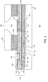
- Fig. 1 is a cross-section diagram of a part of a fluid ejection device 100 according to an example implementation.
- the fluid ejection device 100 is used in a thermal inkjet (TIJ) printhead, for example.
- the fluid ejection device 100 includes a substrate 102, a thin-film stack 150, and a chamber 152 formed on the thin-film stack 150.
- the chamber 152 is formed within a barrier layer 128 and a plate layer 130, each deposited on the thin-film stack 150.
- the chamber 152 is fluidically coupled to a nozzle 132.
- the chamber 152 is configured to hold fluid (e.g., ink), which can be ejected from the nozzle 132.
- fluid e.g., ink
- the substrate 102 is a semiconductor substrate having doped regions, such as a doped region 108 and a doped region 110.
- the doped regions 108 and 110 can form a source and drain of a transistor.
- the thin-film stack 150 includes multiple layers deposited on the substrate 102 in a pattern.
- the layers in the thin-film stack 150 can be deposited and patterned using known semiconductor deposition and processing techniques. It is to be understood that Fig. 1 shows the thin-film stack schematically and omits topology details, such as the varying heights and thicknesses of the layers as they are deposited over the substrate 102. Where such details are necessary for understanding the example implementations, they will be shown in more detail in subsequent drawings described below.
- the thin-film stack 150 includes a gate-oxide (GOX) layer 112, a polysilicon layer 114, a dielectric layer 104, a metal layer 118, a dielectric layer 106, and a metal layer 123.
- the GOX layer 112 is a first layer patterned on the substrate 102.
- the polysilicon layer 114 is patterned on the GOX layer 112. A portion of the polysilicon layer 114 can provide a gate for the transistor formed using the doped regions 108 and 110. Another portion of the polysilicon layer 114 provides a polysilicon structure 116, discussed in further detail below.
- the dielectric layer 104 is deposited over the polysilicon layer 114.
- the dielectric layer 104 can be any type of insulating layer, such as silicon oxide, phosphosilicate glass (PSG), undoped silicate glass (USG), Silicon Carbide (SiC), Silicon Nitride (SiN), tetraethyl orthosilicate (TEOS), or the like, or combinations thereof.
- Vias e.g., 136 and 138 can be formed in the dielectric layer 104 to expose portions of the polysilicon layer 114 and the substrate 102.
- the metal layer 118 is deposited over the dielectric layer 104 and in the vias formed in the dielectric layer 104.
- the metal layer 118 can be formed from Tantalum (Ta), Aluminum (Al), Copper (Cu), Gold (AU), or the like or combinations thereof (e.g., TA and AU), including alloys or combinations thereof (e.g., TaAl, AlCu).
- the metal layer 118 includes multiple conductive layers. For example, conductive layers 120 and 122 are shown.
- the conductive layers 120 and 122 have different sheet resistances (sheet resistance is resistance per unit). For example, the conductive layer 120 has a higher sheet resistance than the conductive layer 122 such that, where the conductive layer 122 is present, the majority of the current goes through the conductive layer 122.
- the conductive layer 122 acts as a conducting line and is used to route signals
- the conductive layer 120 acts as a resistive line, and is used as a resistor.
- the metal layer 118 may be formed by first depositing the conductive layer 120, depositing the conductive layer 122, and then etching the conductive layer 122 to expose portions of the conductive layer 120.
- a portion 134 of the conductive layer 120 under the chamber 152 is exposed.
- the exposed portion 134 provides a surface of a resistor under the chamber 152 thermally coupled to the chamber 152.
- the dielectric layer 106 is deposited over the metal layer 118.
- the dielectric layer 106 can be any type of insulating layer, such as silicon oxide, PSG, USG, SiC, SiN, TEOS, or the like or combinations thereof. Portions of the dielectric layer 106 can be etched to expose portions of the metal layer 118 (e.g., vias can be formed in the dielectric layer 106).
- the metal layer 123 is deposited over the dielectric layer 106 and in the vias formed in the dielectric layer 106.
- the metal layer 123 can be formed from Tantalum (Ta), Aluminum (Al), Copper (Cu), Gold (AU), or the like or combinations thereof (e.g., TA and AU), including alloys or combinations thereof (e.g., TaAl, AlCu).
- the metal layer 123 can include multiple conductive layers, similar to the metal layer 118.
- the metal layer 123 can include a conductive layer 124 and a conductive layer 126.
- the conductive layer 126 can be used to provide a bond pad 140 for receiving electrical signals from an external source (not shown).
- the conductive layer 124 can provide an anti-cavitation layer to mitigate mechanical damage to lower layers under the chamber 152 due to collapse of a fluid bubble therein. In other examples, the conductive layer 124 can be omitted from beneath the chamber 152.
- a resistor may be heated (fired) by sending a current pulse through it. Any appropriate method can be used to direct a current pulse to the desired resistor, for example, direct addressing, matrix addressing, or a smart drive chip in the fluid ejection device 100. Selection of which resistor to fire may be carried out by a processor in the fluid ejection device 100, a processor in a related controlling device, such as a printer, or a combination thereof. Once it has been determined to heat a particular resistor, a pulse of electric current can be delivered to the resistor through circuitry in the fluid ejection device 100.
- Fig. 1 shows an example in which a current pulse may be delivered to a resistor formed from the exposed portion 134 of the conductive layer 120 under the chamber 152.
- the current can be coupled to the bond pad 140, through the metal layer 118, through a transistor formed from the doped regions 108 and 110, and to a portion of the metal layer 118 under the chamber 152 implementing the resistor.
- this signal route is merely an example, and variations and other configurations are possible.
- the layers of the thin-film stack 150 are not shown to scale.
- the layers can have various thicknesses depending on particular device configuration and processes used.
- the GOX layer 112 can have a thickness on the order of 750 Angstroms (A); the polysilicon layer 114 on the order of 3600 A; the dielectric layer 104 on the order of 13000 A; the metal layer 118 on the order of 5000 A; the dielectric layer 106 on the order of 3850 A; and the metal layer 123 on the order of 4600 A.
- these thicknesses are merely an example and variations and other configurations are possible.
- the particular configuration of layers in the thin-film stack 150 is also provided by way of example.
- the thin-film stack 150 as described herein provides a resistor beneath the chamber 152, and a polysilicon structure beneath the resistor.
- the polysilicon structure and its advantages are described immediately below.
- the polysilicon structure 116 can include at least one polysilicon segment (e.g., two are shown in the cross-section).
- the polysilicon layer 114 can have a thickness such that it causes significant topography differences in the metal layer 118 within the exposed portion 134 (e.g., the surface of the resistor). This causes an uneven surface of the resistor, which improves the thermal efficiency of the resistor.
- the topology variation in the resistor surface can achieve lower static turn-on energy (STOE) for the resistor.
- STOE static turn-on energy
- thermal efficiency can only be improved by using either thinner passivation layer (e.g., the dielectric layer 106) or thick thermal barrier underneath the resistor (e.g., the dielectric layer 104).
- a thinner passivation layer is susceptible to pin holes resulting in loss of yield.
- a thicker thermal barrier layer increases cost.
- the polysilicon structure 116 will neither increase cost nor increase real-estate requirements for the die design.
- the polysilicon structure 116 is passive and does not conduct current. In such examples, the polysilicon structure 116 is present only to alter the topology of the resistor surface to improve thermal efficiency. In another example, the polysilicon structure 116 or a portion thereof can be used to conduct current for various purposes. For example, the polysilicon structure 116 or a portion thereof may provide gate(s) for transistor(s) formed in the fluid ejection device 100 (e.g., the polysilicon structure can be part of the gate 114). In another example, the polysilicon structure 116 can be used as a secondary heating element in addition to the resistor since polysilicon has reasonable sheet resistance (e.g., 30 ohm per square). The secondary heater can warm the dielectric layer 104 to relieve heat loss to the silicon substrate 102.
- the secondary heater can warm the dielectric layer 104 to relieve heat loss to the silicon substrate 102.
- Fig. 2 is a cross-section diagram of a resistor portion 200 of a fluid ejection device according to an example implementation. Elements of Fig. 2 that are the same or similar to those of Fig. 1 are designated with identical reference numerals and are described in detail above.
- the resistor portion 200 shows more detail of the fluid ejection device 100 under the chamber 152. The chamber 152 has been omitted for clarity.
- the resistor portion 200 includes the substrate 102, the GOX layer 112, the polysilicon layer 114, the dielectric layer 104, the metal layer 118, the dielectric layer 106, and the conductive layer 124 of the metal layer 123.
- the polysilicon structure 116 is positioned beneath the metal layer 118 forming the resistor.
- the polysilicon structure 116 is beneath the exposed portion of the conductive layer 120 that provides the resistor. Due to the thickness of the polysilicon layer 114, the surface of the conductive layer 120 is uneven (e.g., the surface exhibits "hills” and “valleys”). The “valleys" in the surface of the conductive layer 120 are emphasized by dashed circles 202. The valleys in the conductive layer 120 assist nucleation of fluid bubbles when a current pulse passes through the conductive layer 120 as compared to a flat surface. Thermal efficiency of the resistor is improved.
- the polysilicon structure 116 can include at least one polysilicon segment (e.g., 3 are shown in Fig. 2 ). Various configurations of the polysilicon structure 116 are described below.
- Figs. 3-5 depict top-down views of the resistor portion of a fluid ejection device according to example implementations.
- the resistor surface 302 is shown in dashed outline.
- the polysilicon structure includes a plurality of polysilicon segments 304 arranged in a grid formation.
- a resistor surface 402 is shown in dashed outline.
- the polysilicon structure includes a plurality of segments 404 extending from one side of the resistor surface 402 to another side of the resistor surface 402.
- a resistor surface 502 is shown in dashed outline.
- the polysilicon structure includes a plurality of segments 504 arranged in a serpentine formation.
- the polysilicon structures shown in Figs. 3-5 are mere examples and that structures of different variations and configurations can be provided to alter the surface of the resistor such that the resistor surface becomes uneven providing hills and valleys.
- the polysilicon structures shown in Figs. 3-5 are passive and do not conduct current.
- all or a portion of the polysilicon structure shown in Figs. 4 and 5 can be used for both altering resistor surface topology and another purposes, such as transistor gates or secondary heaters for warming the fluid.
- Fig. 6 is a cross-section diagram of a part of a fluid ejection device 600 according to an example implementation. Elements of Fig. 6 that are the same or similar to those of Fig. 1 are designated with identical reference numerals and described in detail above.
- the device 600 is similar to the device 100, with the exception that the resistor is formed in the second metal layer, and the first metal layer can be used for signal routing.
- the device 600 is another example of using a polysilicon structure under a TIJ resistor to alter the topography of the resistor surface to improve thermal efficiency and STOE. It is to be understood that use of a polysilicon structure under a TIJ resistor can be employed in still further variations/configurations of fluid ejection devices, of which devices 100 and 600 are examples.
- a thin-film stack 650 on the substrate 102 includes a first metal layer 602 deposited on the dielectric layer 104, and a second metal layer 606 deposited on the dielectric 106.
- the metal layers 602 and 606 can be formed from Tantalum (Ta), Aluminum (Al), Copper (Cu), Gold (AU), or the like or combinations thereof (e.g., TA and AU), including alloys or combinations thereof (e.g., TaAl, AlCu).
- a dielectric layer 604 is deposited over the metal layer 606.
- the dielectric layer 604 can be any type of insulating layer, such as silicon oxide, PSG, USG, SiC, SiN, TEOS, or the like, or combinations thereof.
- the metal layer 606 can include multiple conductive layers.
- conductive layers 608 and 610 are shown.
- the conductive layers 608 and 610 can have different sheet resistances (sheet resistance is resistance per unit).
- sheet resistance is resistance per unit.
- the conductive layer 608 has a higher sheet resistance than the conductive layer 610 such that, where the conductive layer 610 is present, the majority of the current goes through the conductive layer 610.
- the conductive layer 610 acts as a conducting line and may be used to route signals
- the conductive layer 608 acts as a resistive line, and may be used as a resistor.
- the metal layer 606 may be formed by first depositing the conductive layer 608, depositing the conductive layer 610, and then etching the conductive layer 610 to expose portions of the conductive layer 608. In particular, a portion 134 of the conductive layer 608 under the chamber 152 is exposed. The exposed portion 134 provides a surface of a resistor under the chamber 152 thermally coupled to the chamber 152. Similar to the device 100, the polysilicon structure 116 causes an un-even surface of the resistor (e.g., uneven surface of the metal layer 608 in the exposed portion 134). Such an uneven surface of the resistor improves the thermal efficiency. In addition, the topology variation in the resistor surface can achieve lower STOE for the resistor.
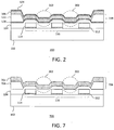
- Fig. 7 is a cross-section diagram of a resistor portion 700 of a fluid ejection device according to an example implementation. Elements of Fig. 7 that are the same or similar to Fig. 2 are designated with identical reference numerals and are described in detail above.
- the device 700 is similar to the device 200, with the exception that the resistor is formed having two conductive layers for the extent of the resistor without an exposed portion having only a single conductive layer.
- the device 700 is another example of using a polysilicon structure under a TIJ resistor to alter the topography of the resistor surface to improve thermal efficiency and STOE.
- resistor portion 700 can be used in place of the resistor portion 200 in devices 100 and 600.
- the resistor portion 700 includes a metal layer 706 deposited on the dielectric 104.
- the metal layer 706 includes a metal layer 702 deposited on a metal layer 704.
- the polysilicon structure 116 causes an un-even surface of the resistor (e.g., uneven surface of the metal layer 702 such that valleys 202 are formed). Such an uneven surface of the resistor improves the thermal efficiency.
- the topology variation in the resistor surface can achieve lower STOE for the resistor.
Landscapes
- Engineering & Computer Science (AREA)
- Manufacturing & Machinery (AREA)
- Particle Formation And Scattering Control In Inkjet Printers (AREA)
Description
- Inkjet technology is widely used for precisely and rapidly dispensing small quantities of fluid. Inkjets eject droplets of fluid out of a nozzle by creating a short pulse of high pressure within a firing chamber. During printing, this ejection process can repeat thousands of times per second. One way to create pressure in the firing chamber is by heating the ink in the firing chamber. A thermal inkjet (TIJ) device include a heating element (e.g., resistor) in the firing chamber. To eject a droplet, an electrical current is passed through the heating element. As the heating element generates heat, a small portion of the fluid within the firing chamber is vaporized. The vapor rapidly expands, forcing a small droplet out of the firing chamber and nozzle. The electrical current is then turned off and the heating element cools. The vapor bubble rapidly collapses, drawing more fluid into the firing chamber.
-
JP 08-216412 - Some example implementations are described with respect to the following figures:
-
Fig. 1 is a cross-section diagram of a part of a fluid ejection device according to an example implementation. -
Fig. 2 is a cross-section diagram of a resistor portion of a fluid ejection device according to an example implementation. -
Figs. 3-5 depict top-down views of the resistor portion of a fluid ejection device according to example implementations. -
Fig. 6 is a cross-section diagram of a part of a fluid ejection device according to another example implementation. -
Fig. 7 is a cross-section diagram of a resistor portion of a fluid ejection device according to another example implementation. -
Fig. 1 is a cross-section diagram of a part of afluid ejection device 100 according to an example implementation. Thefluid ejection device 100 is used in a thermal inkjet (TIJ) printhead, for example. Thefluid ejection device 100 includes asubstrate 102, a thin-film stack 150, and achamber 152 formed on the thin-film stack 150. Thechamber 152 is formed within abarrier layer 128 and aplate layer 130, each deposited on the thin-film stack 150. Thechamber 152 is fluidically coupled to anozzle 132. Thechamber 152 is configured to hold fluid (e.g., ink), which can be ejected from thenozzle 132. - The
substrate 102 is a semiconductor substrate having doped regions, such as adoped region 108 and adoped region 110. The dopedregions film stack 150 includes multiple layers deposited on thesubstrate 102 in a pattern. The layers in the thin-film stack 150 can be deposited and patterned using known semiconductor deposition and processing techniques. It is to be understood thatFig. 1 shows the thin-film stack schematically and omits topology details, such as the varying heights and thicknesses of the layers as they are deposited over thesubstrate 102. Where such details are necessary for understanding the example implementations, they will be shown in more detail in subsequent drawings described below. - In an example, the thin-
film stack 150 includes a gate-oxide (GOX)layer 112, apolysilicon layer 114, adielectric layer 104, ametal layer 118, adielectric layer 106, and ametal layer 123. The GOXlayer 112 is a first layer patterned on thesubstrate 102. Thepolysilicon layer 114 is patterned on the GOXlayer 112. A portion of thepolysilicon layer 114 can provide a gate for the transistor formed using thedoped regions polysilicon layer 114 provides apolysilicon structure 116, discussed in further detail below. - The
dielectric layer 104 is deposited over thepolysilicon layer 114. Thedielectric layer 104 can be any type of insulating layer, such as silicon oxide, phosphosilicate glass (PSG), undoped silicate glass (USG), Silicon Carbide (SiC), Silicon Nitride (SiN), tetraethyl orthosilicate (TEOS), or the like, or combinations thereof. Vias (e.g., 136 and 138) can be formed in thedielectric layer 104 to expose portions of thepolysilicon layer 114 and thesubstrate 102. - The
metal layer 118 is deposited over thedielectric layer 104 and in the vias formed in thedielectric layer 104. Themetal layer 118 can be formed from Tantalum (Ta), Aluminum (Al), Copper (Cu), Gold (AU), or the like or combinations thereof (e.g., TA and AU), including alloys or combinations thereof (e.g., TaAl, AlCu). Themetal layer 118 includes multiple conductive layers. For example,conductive layers conductive layers conductive layer 120 has a higher sheet resistance than theconductive layer 122 such that, where theconductive layer 122 is present, the majority of the current goes through theconductive layer 122. Thus, theconductive layer 122 acts as a conducting line and is used to route signals, and theconductive layer 120 acts as a resistive line, and is used as a resistor. Themetal layer 118 may be formed by first depositing theconductive layer 120, depositing theconductive layer 122, and then etching theconductive layer 122 to expose portions of theconductive layer 120. In particular, aportion 134 of theconductive layer 120 under thechamber 152 is exposed. The exposedportion 134 provides a surface of a resistor under thechamber 152 thermally coupled to thechamber 152. - The
dielectric layer 106 is deposited over themetal layer 118. Thedielectric layer 106 can be any type of insulating layer, such as silicon oxide, PSG, USG, SiC, SiN, TEOS, or the like or combinations thereof. Portions of thedielectric layer 106 can be etched to expose portions of the metal layer 118 (e.g., vias can be formed in the dielectric layer 106). - The
metal layer 123 is deposited over thedielectric layer 106 and in the vias formed in thedielectric layer 106. Themetal layer 123 can be formed from Tantalum (Ta), Aluminum (Al), Copper (Cu), Gold (AU), or the like or combinations thereof (e.g., TA and AU), including alloys or combinations thereof (e.g., TaAl, AlCu). Themetal layer 123 can include multiple conductive layers, similar to themetal layer 118. For example, themetal layer 123 can include aconductive layer 124 and aconductive layer 126. Theconductive layer 126 can be used to provide abond pad 140 for receiving electrical signals from an external source (not shown). In some examples, theconductive layer 124 can provide an anti-cavitation layer to mitigate mechanical damage to lower layers under thechamber 152 due to collapse of a fluid bubble therein. In other examples, theconductive layer 124 can be omitted from beneath thechamber 152. - A resistor may be heated (fired) by sending a current pulse through it. Any appropriate method can be used to direct a current pulse to the desired resistor, for example, direct addressing, matrix addressing, or a smart drive chip in the
fluid ejection device 100. Selection of which resistor to fire may be carried out by a processor in thefluid ejection device 100, a processor in a related controlling device, such as a printer, or a combination thereof. Once it has been determined to heat a particular resistor, a pulse of electric current can be delivered to the resistor through circuitry in thefluid ejection device 100. -
Fig. 1 shows an example in which a current pulse may be delivered to a resistor formed from the exposedportion 134 of theconductive layer 120 under thechamber 152. The current can be coupled to thebond pad 140, through themetal layer 118, through a transistor formed from the dopedregions metal layer 118 under thechamber 152 implementing the resistor. Of course, this signal route is merely an example, and variations and other configurations are possible. - It is to be understood that the layers of the thin-
film stack 150 are not shown to scale. The layers can have various thicknesses depending on particular device configuration and processes used. In an example, theGOX layer 112 can have a thickness on the order of 750 Angstroms (A); thepolysilicon layer 114 on the order of 3600 A; thedielectric layer 104 on the order of 13000 A; themetal layer 118 on the order of 5000 A; thedielectric layer 106 on the order of 3850 A; and themetal layer 123 on the order of 4600 A. Of course, these thicknesses are merely an example and variations and other configurations are possible. Moreover, the particular configuration of layers in the thin-film stack 150 is also provided by way of example. It is to be understood that additional dielectric and/or metal layers can be provided in different configurations. In general, the thin-film stack 150 as described herein provides a resistor beneath thechamber 152, and a polysilicon structure beneath the resistor. The polysilicon structure and its advantages are described immediately below. - The
polysilicon structure 116 can include at least one polysilicon segment (e.g., two are shown in the cross-section). Thepolysilicon layer 114 can have a thickness such that it causes significant topography differences in themetal layer 118 within the exposed portion 134 (e.g., the surface of the resistor). This causes an uneven surface of the resistor, which improves the thermal efficiency of the resistor. In addition, the topology variation in the resistor surface can achieve lower static turn-on energy (STOE) for the resistor. Without thepolysilicon structure 116, thermal efficiency can only be improved by using either thinner passivation layer (e.g., the dielectric layer 106) or thick thermal barrier underneath the resistor (e.g., the dielectric layer 104). A thinner passivation layer, however, is susceptible to pin holes resulting in loss of yield. A thicker thermal barrier layer increases cost. Thepolysilicon structure 116 will neither increase cost nor increase real-estate requirements for the die design. - In one example, the
polysilicon structure 116 is passive and does not conduct current. In such examples, thepolysilicon structure 116 is present only to alter the topology of the resistor surface to improve thermal efficiency. In another example, thepolysilicon structure 116 or a portion thereof can be used to conduct current for various purposes. For example, thepolysilicon structure 116 or a portion thereof may provide gate(s) for transistor(s) formed in the fluid ejection device 100 (e.g., the polysilicon structure can be part of the gate 114). In another example, thepolysilicon structure 116 can be used as a secondary heating element in addition to the resistor since polysilicon has reasonable sheet resistance (e.g., 30 ohm per square). The secondary heater can warm thedielectric layer 104 to relieve heat loss to thesilicon substrate 102. -
Fig. 2 is a cross-section diagram of aresistor portion 200 of a fluid ejection device according to an example implementation. Elements ofFig. 2 that are the same or similar to those ofFig. 1 are designated with identical reference numerals and are described in detail above. Theresistor portion 200 shows more detail of thefluid ejection device 100 under thechamber 152. Thechamber 152 has been omitted for clarity. Theresistor portion 200 includes thesubstrate 102, theGOX layer 112, thepolysilicon layer 114, thedielectric layer 104, themetal layer 118, thedielectric layer 106, and theconductive layer 124 of themetal layer 123. Thepolysilicon structure 116 is positioned beneath themetal layer 118 forming the resistor. In particular, thepolysilicon structure 116 is beneath the exposed portion of theconductive layer 120 that provides the resistor. Due to the thickness of thepolysilicon layer 114, the surface of theconductive layer 120 is uneven (e.g., the surface exhibits "hills" and "valleys"). The "valleys" in the surface of theconductive layer 120 are emphasized by dashedcircles 202. The valleys in theconductive layer 120 assist nucleation of fluid bubbles when a current pulse passes through theconductive layer 120 as compared to a flat surface. Thermal efficiency of the resistor is improved. Thepolysilicon structure 116 can include at least one polysilicon segment (e.g., 3 are shown inFig. 2 ). Various configurations of thepolysilicon structure 116 are described below. -
Figs. 3-5 depict top-down views of the resistor portion of a fluid ejection device according to example implementations. As shown inFig. 3 , theresistor surface 302 is shown in dashed outline. The polysilicon structure includes a plurality ofpolysilicon segments 304 arranged in a grid formation. As shown inFig. 4 , aresistor surface 402 is shown in dashed outline. The polysilicon structure includes a plurality ofsegments 404 extending from one side of theresistor surface 402 to another side of theresistor surface 402. As shown inFig. 5 , aresistor surface 502 is shown in dashed outline. The polysilicon structure includes a plurality ofsegments 504 arranged in a serpentine formation. It is to be understood that the polysilicon structures shown inFigs. 3-5 are mere examples and that structures of different variations and configurations can be provided to alter the surface of the resistor such that the resistor surface becomes uneven providing hills and valleys. In some examples, the polysilicon structures shown inFigs. 3-5 are passive and do not conduct current. In other examples, all or a portion of the polysilicon structure shown inFigs. 4 and 5 can be used for both altering resistor surface topology and another purposes, such as transistor gates or secondary heaters for warming the fluid. -
Fig. 6 is a cross-section diagram of a part of afluid ejection device 600 according to an example implementation. Elements ofFig. 6 that are the same or similar to those ofFig. 1 are designated with identical reference numerals and described in detail above. Thedevice 600 is similar to thedevice 100, with the exception that the resistor is formed in the second metal layer, and the first metal layer can be used for signal routing. Thedevice 600 is another example of using a polysilicon structure under a TIJ resistor to alter the topography of the resistor surface to improve thermal efficiency and STOE. It is to be understood that use of a polysilicon structure under a TIJ resistor can be employed in still further variations/configurations of fluid ejection devices, of whichdevices - A thin-
film stack 650 on thesubstrate 102 includes afirst metal layer 602 deposited on thedielectric layer 104, and asecond metal layer 606 deposited on the dielectric 106. The metal layers 602 and 606 can be formed from Tantalum (Ta), Aluminum (Al), Copper (Cu), Gold (AU), or the like or combinations thereof (e.g., TA and AU), including alloys or combinations thereof (e.g., TaAl, AlCu). Adielectric layer 604 is deposited over themetal layer 606. Thedielectric layer 604 can be any type of insulating layer, such as silicon oxide, PSG, USG, SiC, SiN, TEOS, or the like, or combinations thereof. - The
metal layer 606 can include multiple conductive layers. For example,conductive layers conductive layers conductive layer 608 has a higher sheet resistance than theconductive layer 610 such that, where theconductive layer 610 is present, the majority of the current goes through theconductive layer 610. Thus, theconductive layer 610 acts as a conducting line and may be used to route signals, and theconductive layer 608 acts as a resistive line, and may be used as a resistor. Themetal layer 606 may be formed by first depositing theconductive layer 608, depositing theconductive layer 610, and then etching theconductive layer 610 to expose portions of theconductive layer 608. In particular, aportion 134 of theconductive layer 608 under thechamber 152 is exposed. The exposedportion 134 provides a surface of a resistor under thechamber 152 thermally coupled to thechamber 152. Similar to thedevice 100, thepolysilicon structure 116 causes an un-even surface of the resistor (e.g., uneven surface of themetal layer 608 in the exposed portion 134). Such an uneven surface of the resistor improves the thermal efficiency. In addition, the topology variation in the resistor surface can achieve lower STOE for the resistor. -
Fig. 7 is a cross-section diagram of aresistor portion 700 of a fluid ejection device according to an example implementation. Elements ofFig. 7 that are the same or similar toFig. 2 are designated with identical reference numerals and are described in detail above. Thedevice 700 is similar to thedevice 200, with the exception that the resistor is formed having two conductive layers for the extent of the resistor without an exposed portion having only a single conductive layer. Thedevice 700 is another example of using a polysilicon structure under a TIJ resistor to alter the topography of the resistor surface to improve thermal efficiency and STOE. It is to be understood that use of a polysilicon structure under a TIJ resistor can be employed in still further variations/configurations of resistor designs, of whichdevices resistor portion 700 can be used in place of theresistor portion 200 indevices - The
resistor portion 700 includes ametal layer 706 deposited on the dielectric 104. Themetal layer 706 includes ametal layer 702 deposited on a metal layer 704. Similar to thedevice 200, thepolysilicon structure 116 causes an un-even surface of the resistor (e.g., uneven surface of themetal layer 702 such thatvalleys 202 are formed). Such an uneven surface of the resistor improves the thermal efficiency. In addition, the topology variation in the resistor surface can achieve lower STOE for the resistor.
Claims (7)
- A thermal fluid ejection device (100), comprising:a substrate (102) having a chamber (152) formed thereon to contain a fluida metal layer (118) comprising a resistor (120) having a surface (302, 402, 502) thermally coupled to the chamber (152);a first and a second conductive layers (120, 122) formed in the metal layer (118);a polysilicon layer (114) under the metal layer (118) comprising a polysilicon structure (116) under the resistor (120) to change the topography of the resistor (120) such that the surface thermally coupled to the chamber (152) is uneven, the polysilicon structure (116) including a plurality of segments (304, 404, 504); anda first dielectric layer (104) between the polysilicon layer (114) and the metal layer (118),wherein the first conductive layer (120) is used as the resistor (120) and has higher sheet resistance than the second conductive layer (122).
- The thermal fluid ejection device of claim 1, the first conductive layer (120) linking two separate portions of the second conductive layer (122), where the surface thermally coupled to the chamber (152) comprises the portion (134) of the first conductive layer (120) between the two separate portions of the second conductive layer (122).
- The thermal fluid ejection device of claim 1, wherein the plurality of segments (304, 404, 504) are formed in a grid.
- The thermal fluid ejection device of claim 1, further comprising a second dielectric layer (106) over the metal layer (118) and an anti-cavitation layer (124).
- A printhead for a printer, comprising:the thermal fluid ejection device (100) according to any of the preceding claims;at least one nozzle (132) fluidically coupled to the chamber (152); anda thin-film stack (150) under the chamber (152), including:the metal layer (118) comprising the resistor (120) having a surface thermally coupled to the chamber (152); andthe polysilicon layer (114).
- A method of manufacturing a fluid ejection device, comprising:forming a polysilicon layer (114) on a substrate (102);forming a dielectric layer (104) over the polysilicon layer (114);forming a metal layer (118) comprising a resistor (120) over the dielectric layer (104) and a conductive layer (122) on the resistor (120); andforming a chamber (152) over the resistor (120) to contain a fluid;wherein the resistor (120) is formed to have a surface (302, 402, 502) thermally coupled to the chamber (152);wherein the polysilicon layer (114) includes a polysilicon structure (116), with a plurality of segments (304, 404, 504), under the resistor (120) to change the topography of the resistor (120) such that the surface thermally coupled to the chamber (152) is uneven,the resistor (120) having higher sheet resistance than the conductive layer (122).
- The method of claim 6, the resistor (120) linking two separate portions of the conductive layer (122), where the surface (302, 402, 502) thermally coupled to the chamber (152) comprises the portion (134) of the resistor (120) between the two separate portions of the conductive layer (122).
Applications Claiming Priority (1)
| Application Number | Priority Date | Filing Date | Title |
|---|---|---|---|
| PCT/US2013/052460 WO2015016806A1 (en) | 2013-07-29 | 2013-07-29 | Fluid ejection device |
Publications (3)
| Publication Number | Publication Date |
|---|---|
| EP2978609A1 EP2978609A1 (en) | 2016-02-03 |
| EP2978609A4 EP2978609A4 (en) | 2017-05-17 |
| EP2978609B1 true EP2978609B1 (en) | 2021-04-21 |
Family
ID=52432183
Family Applications (1)
| Application Number | Title | Priority Date | Filing Date |
|---|---|---|---|
| EP13890258.0A Active EP2978609B1 (en) | 2013-07-29 | 2013-07-29 | Fluid ejection device and a method of manufacturing a fluid ejection device |
Country Status (4)
| Country | Link |
|---|---|
| US (2) | US9676187B2 (en) |
| EP (1) | EP2978609B1 (en) |
| CN (1) | CN105163943B (en) |
| WO (1) | WO2015016806A1 (en) |
Families Citing this family (8)
| Publication number | Priority date | Publication date | Assignee | Title |
|---|---|---|---|---|
| CN105163943B (en) * | 2013-07-29 | 2017-06-23 | 惠普发展公司,有限责任合伙企业 | Fluid discharge apparatus |
| US11225086B2 (en) | 2017-03-15 | 2022-01-18 | Hewlett-Packard Development Company, L.P. | Thermal contact dies |
| JP7094772B2 (en) * | 2017-06-20 | 2022-07-04 | キヤノン株式会社 | Liquid discharge head and liquid discharge device |
| JP7191669B2 (en) * | 2018-12-17 | 2022-12-19 | キヤノン株式会社 | SUBSTRATE FOR LIQUID EJECTION HEAD AND MANUFACTURING METHOD THEREOF |
| JP7344669B2 (en) * | 2019-04-23 | 2023-09-14 | キヤノン株式会社 | Element substrate, liquid ejection head, and recording device |
| JP7328787B2 (en) * | 2019-04-23 | 2023-08-17 | キヤノン株式会社 | ELEMENT SUBSTRATE, LIQUID EJECTION HEAD, AND RECORDING APPARATUS |
| CN115810669A (en) | 2021-09-14 | 2023-03-17 | 群创光电股份有限公司 | Heating device and manufacturing method thereof |
| US20240194729A1 (en) * | 2022-12-13 | 2024-06-13 | Psemi Corporation | Three-Dimensional Integrated Circuit Resistors |
Family Cites Families (19)
| Publication number | Priority date | Publication date | Assignee | Title |
|---|---|---|---|---|
| JPS5783477A (en) * | 1980-11-14 | 1982-05-25 | Toshiba Corp | Thermal print head |
| US5081473A (en) | 1990-07-26 | 1992-01-14 | Xerox Corporation | Temperature control transducer and MOS driver for thermal ink jet printing chips |
| US5169806A (en) * | 1990-09-26 | 1992-12-08 | Xerox Corporation | Method of making amorphous deposited polycrystalline silicon thermal ink jet transducers |
| JPH08216412A (en) * | 1995-02-15 | 1996-08-27 | Canon Inc | Inkjet recording head and inkjet recording apparatus including the head |
| DE69622147T2 (en) * | 1996-03-04 | 2002-11-14 | Hewlett-Packard Co. (N.D.Ges.D.Staates Delaware), Palo Alto | Ink jet pens have a heating element with a profiled surface |
| US5943076A (en) | 1997-02-24 | 1999-08-24 | Xerox Corporation | Printhead for thermal ink jet devices |
| US6379620B1 (en) * | 1998-11-16 | 2002-04-30 | Barry M. Tydings | Assaying device and method for in field urinalysis |
| US6315384B1 (en) | 1999-03-08 | 2001-11-13 | Hewlett-Packard Company | Thermal inkjet printhead and high-efficiency polycrystalline silicon resistor system for use therein |
| US6299294B1 (en) | 1999-07-29 | 2001-10-09 | Hewlett-Packard Company | High efficiency printhead containing a novel oxynitride-based resistor system |
| JP2001121702A (en) * | 1999-10-27 | 2001-05-08 | Sharp Corp | INK JET HEAD AND CONTROL METHOD THEREOF |
| JP2002067321A (en) * | 2000-08-31 | 2002-03-05 | Kyocera Corp | Inkjet head |
| TWI232807B (en) | 2001-01-19 | 2005-05-21 | Benq Corp | Microinject head with driving circuitry and the manufacturing method thereof |
| US6457815B1 (en) * | 2001-01-29 | 2002-10-01 | Hewlett-Packard Company | Fluid-jet printhead and method of fabricating a fluid-jet printhead |
| JP2005041176A (en) | 2003-07-25 | 2005-02-17 | Fuji Xerox Co Ltd | Heating resistor and its producing process, ink jet recording head and its manufacturing process |
| US8361414B2 (en) | 2005-01-06 | 2013-01-29 | Shimadzu Corporation | Gas exchange chip |
| GB0500114D0 (en) | 2005-01-06 | 2005-02-09 | Koninkl Philips Electronics Nv | Inkjet print head |
| KR101726934B1 (en) * | 2010-07-23 | 2017-04-13 | 휴렛-팩커드 디벨롭먼트 컴퍼니, 엘.피. | Thermal resistor fluid ejection assembly |
| US8449079B2 (en) * | 2011-09-13 | 2013-05-28 | Hewlett-Packard Development Company, L.P. | Fluid ejection device having first and second resistors |
| CN105163943B (en) * | 2013-07-29 | 2017-06-23 | 惠普发展公司,有限责任合伙企业 | Fluid discharge apparatus |
-
2013
- 2013-07-29 CN CN201380076167.XA patent/CN105163943B/en not_active Expired - Fee Related
- 2013-07-29 EP EP13890258.0A patent/EP2978609B1/en active Active
- 2013-07-29 WO PCT/US2013/052460 patent/WO2015016806A1/en not_active Ceased
- 2013-07-29 US US14/787,233 patent/US9676187B2/en not_active Expired - Fee Related
-
2017
- 2017-05-12 US US15/594,068 patent/US9914297B2/en not_active Expired - Fee Related
Non-Patent Citations (1)
| Title |
|---|
| None * |
Also Published As
| Publication number | Publication date |
|---|---|
| US9914297B2 (en) | 2018-03-13 |
| CN105163943B (en) | 2017-06-23 |
| US20160114580A1 (en) | 2016-04-28 |
| EP2978609A4 (en) | 2017-05-17 |
| US9676187B2 (en) | 2017-06-13 |
| WO2015016806A1 (en) | 2015-02-05 |
| EP2978609A1 (en) | 2016-02-03 |
| US20170246866A1 (en) | 2017-08-31 |
| CN105163943A (en) | 2015-12-16 |
Similar Documents
| Publication | Publication Date | Title |
|---|---|---|
| US9914297B2 (en) | Fluid ejection device | |
| CN105939857B (en) | Hot ink-jet print head | |
| EP1413438B1 (en) | Monolithic ink-jet printhead with tapered nozzle and method for manufcturing the same | |
| US9156254B2 (en) | Fluid ejection device | |
| JP2004306585A (en) | Integrated ink-jet printhead having a heater disposed between two ink chambers and method of manufacturing the same | |
| KR100911323B1 (en) | Heat generating structure for inkjet printhead and inkjet printhead having same | |
| KR20050000601A (en) | Inkjet printhead | |
| WO2010011250A2 (en) | Printhead having isolated heater | |
| EP3160751B1 (en) | Fluid ejection structure | |
| JP2005022402A (en) | Inkjet print head | |
| US7073891B2 (en) | Monolithic ink-jet printhead having a metal nozzle plate and manufacturing method thereof | |
| JP2004351931A (en) | INK JET PRINT HEAD AND ITS MANUFACTURING METHOD | |
| US7101024B2 (en) | Ink-jet printhead | |
| US7390078B2 (en) | Reduction of heat loss in micro-fluid ejection devices | |
| US20090267996A1 (en) | Heater stack with enhanced protective strata structure and methods for making enhanced heater stack | |
| JP2005022413A (en) | Inkjet printhead driving method | |
| KR100723414B1 (en) | Thermal inkjet printheads | |
| JP2005047270A (en) | Ink jet print head and manufacturing method thereof | |
| KR100513717B1 (en) | Bubble-jet type inkjet printhead | |
| KR100446633B1 (en) | Ink jet printhead | |
| KR20060070696A (en) | Thermal inkjet inkjet printhead and its manufacturing method | |
| KR20060069564A (en) | Inkjet print head |
Legal Events
| Date | Code | Title | Description |
|---|---|---|---|
| PUAI | Public reference made under article 153(3) epc to a published international application that has entered the european phase |
Free format text: ORIGINAL CODE: 0009012 |
|
| 17P | Request for examination filed |
Effective date: 20151030 |
|
| AK | Designated contracting states |
Kind code of ref document: A1 Designated state(s): AL AT BE BG CH CY CZ DE DK EE ES FI FR GB GR HR HU IE IS IT LI LT LU LV MC MK MT NL NO PL PT RO RS SE SI SK SM TR |
|
| AX | Request for extension of the european patent |
Extension state: BA ME |
|
| DAX | Request for extension of the european patent (deleted) | ||
| A4 | Supplementary search report drawn up and despatched |
Effective date: 20170413 |
|
| RIC1 | Information provided on ipc code assigned before grant |
Ipc: B41J 2/355 20060101AFI20170408BHEP |
|
| STAA | Information on the status of an ep patent application or granted ep patent |
Free format text: STATUS: EXAMINATION IS IN PROGRESS |
|
| 17Q | First examination report despatched |
Effective date: 20181116 |
|
| RAP1 | Party data changed (applicant data changed or rights of an application transferred) |
Owner name: HEWLETT-PACKARD DEVELOPMENT COMPANY, L.P. |
|
| REG | Reference to a national code |
Ref country code: DE Ref legal event code: R079 Ref document number: 602013077082 Country of ref document: DE Free format text: PREVIOUS MAIN CLASS: B41J0002355000 Ipc: B41J0002140000 |
|
| GRAP | Despatch of communication of intention to grant a patent |
Free format text: ORIGINAL CODE: EPIDOSNIGR1 |
|
| STAA | Information on the status of an ep patent application or granted ep patent |
Free format text: STATUS: GRANT OF PATENT IS INTENDED |
|
| INTG | Intention to grant announced |
Effective date: 20210104 |
|
| RIC1 | Information provided on ipc code assigned before grant |
Ipc: B41J 2/14 20060101AFI20201211BHEP |
|
| INTG | Intention to grant announced |
Effective date: 20210114 |
|
| GRAS | Grant fee paid |
Free format text: ORIGINAL CODE: EPIDOSNIGR3 |
|
| GRAA | (expected) grant |
Free format text: ORIGINAL CODE: 0009210 |
|
| STAA | Information on the status of an ep patent application or granted ep patent |
Free format text: STATUS: THE PATENT HAS BEEN GRANTED |
|
| AK | Designated contracting states |
Kind code of ref document: B1 Designated state(s): AL AT BE BG CH CY CZ DE DK EE ES FI FR GB GR HR HU IE IS IT LI LT LU LV MC MK MT NL NO PL PT RO RS SE SI SK SM TR |
|
| REG | Reference to a national code |
Ref country code: GB Ref legal event code: FG4D |
|
| REG | Reference to a national code |
Ref country code: CH Ref legal event code: EP |
|
| REG | Reference to a national code |
Ref country code: DE Ref legal event code: R096 Ref document number: 602013077082 Country of ref document: DE |
|
| REG | Reference to a national code |
Ref country code: IE Ref legal event code: FG4D |
|
| REG | Reference to a national code |
Ref country code: AT Ref legal event code: REF Ref document number: 1384231 Country of ref document: AT Kind code of ref document: T Effective date: 20210515 |
|
| REG | Reference to a national code |
Ref country code: LT Ref legal event code: MG9D |
|
| REG | Reference to a national code |
Ref country code: AT Ref legal event code: MK05 Ref document number: 1384231 Country of ref document: AT Kind code of ref document: T Effective date: 20210421 |
|
| REG | Reference to a national code |
Ref country code: NL Ref legal event code: MP Effective date: 20210421 |
|
| PG25 | Lapsed in a contracting state [announced via postgrant information from national office to epo] |
Ref country code: BG Free format text: LAPSE BECAUSE OF FAILURE TO SUBMIT A TRANSLATION OF THE DESCRIPTION OR TO PAY THE FEE WITHIN THE PRESCRIBED TIME-LIMIT Effective date: 20210721 Ref country code: AT Free format text: LAPSE BECAUSE OF FAILURE TO SUBMIT A TRANSLATION OF THE DESCRIPTION OR TO PAY THE FEE WITHIN THE PRESCRIBED TIME-LIMIT Effective date: 20210421 Ref country code: FI Free format text: LAPSE BECAUSE OF FAILURE TO SUBMIT A TRANSLATION OF THE DESCRIPTION OR TO PAY THE FEE WITHIN THE PRESCRIBED TIME-LIMIT Effective date: 20210421 Ref country code: LT Free format text: LAPSE BECAUSE OF FAILURE TO SUBMIT A TRANSLATION OF THE DESCRIPTION OR TO PAY THE FEE WITHIN THE PRESCRIBED TIME-LIMIT Effective date: 20210421 Ref country code: NL Free format text: LAPSE BECAUSE OF FAILURE TO SUBMIT A TRANSLATION OF THE DESCRIPTION OR TO PAY THE FEE WITHIN THE PRESCRIBED TIME-LIMIT Effective date: 20210421 Ref country code: HR Free format text: LAPSE BECAUSE OF FAILURE TO SUBMIT A TRANSLATION OF THE DESCRIPTION OR TO PAY THE FEE WITHIN THE PRESCRIBED TIME-LIMIT Effective date: 20210421 |
|
| PG25 | Lapsed in a contracting state [announced via postgrant information from national office to epo] |
Ref country code: LV Free format text: LAPSE BECAUSE OF FAILURE TO SUBMIT A TRANSLATION OF THE DESCRIPTION OR TO PAY THE FEE WITHIN THE PRESCRIBED TIME-LIMIT Effective date: 20210421 Ref country code: GR Free format text: LAPSE BECAUSE OF FAILURE TO SUBMIT A TRANSLATION OF THE DESCRIPTION OR TO PAY THE FEE WITHIN THE PRESCRIBED TIME-LIMIT Effective date: 20210722 Ref country code: IS Free format text: LAPSE BECAUSE OF FAILURE TO SUBMIT A TRANSLATION OF THE DESCRIPTION OR TO PAY THE FEE WITHIN THE PRESCRIBED TIME-LIMIT Effective date: 20210821 Ref country code: RS Free format text: LAPSE BECAUSE OF FAILURE TO SUBMIT A TRANSLATION OF THE DESCRIPTION OR TO PAY THE FEE WITHIN THE PRESCRIBED TIME-LIMIT Effective date: 20210421 Ref country code: SE Free format text: LAPSE BECAUSE OF FAILURE TO SUBMIT A TRANSLATION OF THE DESCRIPTION OR TO PAY THE FEE WITHIN THE PRESCRIBED TIME-LIMIT Effective date: 20210421 Ref country code: PL Free format text: LAPSE BECAUSE OF FAILURE TO SUBMIT A TRANSLATION OF THE DESCRIPTION OR TO PAY THE FEE WITHIN THE PRESCRIBED TIME-LIMIT Effective date: 20210421 Ref country code: NO Free format text: LAPSE BECAUSE OF FAILURE TO SUBMIT A TRANSLATION OF THE DESCRIPTION OR TO PAY THE FEE WITHIN THE PRESCRIBED TIME-LIMIT Effective date: 20210721 Ref country code: PT Free format text: LAPSE BECAUSE OF FAILURE TO SUBMIT A TRANSLATION OF THE DESCRIPTION OR TO PAY THE FEE WITHIN THE PRESCRIBED TIME-LIMIT Effective date: 20210823 Ref country code: ES Free format text: LAPSE BECAUSE OF FAILURE TO SUBMIT A TRANSLATION OF THE DESCRIPTION OR TO PAY THE FEE WITHIN THE PRESCRIBED TIME-LIMIT Effective date: 20210421 |
|
| PGFP | Annual fee paid to national office [announced via postgrant information from national office to epo] |
Ref country code: DE Payment date: 20210622 Year of fee payment: 9 |
|
| REG | Reference to a national code |
Ref country code: DE Ref legal event code: R097 Ref document number: 602013077082 Country of ref document: DE |
|
| PG25 | Lapsed in a contracting state [announced via postgrant information from national office to epo] |
Ref country code: RO Free format text: LAPSE BECAUSE OF FAILURE TO SUBMIT A TRANSLATION OF THE DESCRIPTION OR TO PAY THE FEE WITHIN THE PRESCRIBED TIME-LIMIT Effective date: 20210421 Ref country code: SK Free format text: LAPSE BECAUSE OF FAILURE TO SUBMIT A TRANSLATION OF THE DESCRIPTION OR TO PAY THE FEE WITHIN THE PRESCRIBED TIME-LIMIT Effective date: 20210421 Ref country code: SM Free format text: LAPSE BECAUSE OF FAILURE TO SUBMIT A TRANSLATION OF THE DESCRIPTION OR TO PAY THE FEE WITHIN THE PRESCRIBED TIME-LIMIT Effective date: 20210421 Ref country code: EE Free format text: LAPSE BECAUSE OF FAILURE TO SUBMIT A TRANSLATION OF THE DESCRIPTION OR TO PAY THE FEE WITHIN THE PRESCRIBED TIME-LIMIT Effective date: 20210421 Ref country code: DK Free format text: LAPSE BECAUSE OF FAILURE TO SUBMIT A TRANSLATION OF THE DESCRIPTION OR TO PAY THE FEE WITHIN THE PRESCRIBED TIME-LIMIT Effective date: 20210421 Ref country code: CZ Free format text: LAPSE BECAUSE OF FAILURE TO SUBMIT A TRANSLATION OF THE DESCRIPTION OR TO PAY THE FEE WITHIN THE PRESCRIBED TIME-LIMIT Effective date: 20210421 |
|
| PLBE | No opposition filed within time limit |
Free format text: ORIGINAL CODE: 0009261 |
|
| STAA | Information on the status of an ep patent application or granted ep patent |
Free format text: STATUS: NO OPPOSITION FILED WITHIN TIME LIMIT |
|
| REG | Reference to a national code |
Ref country code: CH Ref legal event code: PL |
|
| GBPC | Gb: european patent ceased through non-payment of renewal fee |
Effective date: 20210729 |
|
| 26N | No opposition filed |
Effective date: 20220124 |
|
| PG25 | Lapsed in a contracting state [announced via postgrant information from national office to epo] |
Ref country code: MC Free format text: LAPSE BECAUSE OF FAILURE TO SUBMIT A TRANSLATION OF THE DESCRIPTION OR TO PAY THE FEE WITHIN THE PRESCRIBED TIME-LIMIT Effective date: 20210421 |
|
| REG | Reference to a national code |
Ref country code: BE Ref legal event code: MM Effective date: 20210731 |
|
| PG25 | Lapsed in a contracting state [announced via postgrant information from national office to epo] |
Ref country code: LI Free format text: LAPSE BECAUSE OF NON-PAYMENT OF DUE FEES Effective date: 20210731 Ref country code: GB Free format text: LAPSE BECAUSE OF NON-PAYMENT OF DUE FEES Effective date: 20210729 Ref country code: CH Free format text: LAPSE BECAUSE OF NON-PAYMENT OF DUE FEES Effective date: 20210731 |
|
| PG25 | Lapsed in a contracting state [announced via postgrant information from national office to epo] |
Ref country code: IS Free format text: LAPSE BECAUSE OF FAILURE TO SUBMIT A TRANSLATION OF THE DESCRIPTION OR TO PAY THE FEE WITHIN THE PRESCRIBED TIME-LIMIT Effective date: 20210821 Ref country code: LU Free format text: LAPSE BECAUSE OF NON-PAYMENT OF DUE FEES Effective date: 20210729 Ref country code: FR Free format text: LAPSE BECAUSE OF NON-PAYMENT OF DUE FEES Effective date: 20210731 Ref country code: AL Free format text: LAPSE BECAUSE OF FAILURE TO SUBMIT A TRANSLATION OF THE DESCRIPTION OR TO PAY THE FEE WITHIN THE PRESCRIBED TIME-LIMIT Effective date: 20210421 |
|
| PG25 | Lapsed in a contracting state [announced via postgrant information from national office to epo] |
Ref country code: IT Free format text: LAPSE BECAUSE OF FAILURE TO SUBMIT A TRANSLATION OF THE DESCRIPTION OR TO PAY THE FEE WITHIN THE PRESCRIBED TIME-LIMIT Effective date: 20210421 Ref country code: IE Free format text: LAPSE BECAUSE OF NON-PAYMENT OF DUE FEES Effective date: 20210729 Ref country code: BE Free format text: LAPSE BECAUSE OF NON-PAYMENT OF DUE FEES Effective date: 20210731 |
|
| REG | Reference to a national code |
Ref country code: DE Ref legal event code: R119 Ref document number: 602013077082 Country of ref document: DE |
|
| PG25 | Lapsed in a contracting state [announced via postgrant information from national office to epo] |
Ref country code: HU Free format text: LAPSE BECAUSE OF FAILURE TO SUBMIT A TRANSLATION OF THE DESCRIPTION OR TO PAY THE FEE WITHIN THE PRESCRIBED TIME-LIMIT; INVALID AB INITIO Effective date: 20130729 Ref country code: DE Free format text: LAPSE BECAUSE OF NON-PAYMENT OF DUE FEES Effective date: 20230201 |
|
| PG25 | Lapsed in a contracting state [announced via postgrant information from national office to epo] |
Ref country code: CY Free format text: LAPSE BECAUSE OF FAILURE TO SUBMIT A TRANSLATION OF THE DESCRIPTION OR TO PAY THE FEE WITHIN THE PRESCRIBED TIME-LIMIT Effective date: 20210421 |
|
| PG25 | Lapsed in a contracting state [announced via postgrant information from national office to epo] |
Ref country code: MK Free format text: LAPSE BECAUSE OF FAILURE TO SUBMIT A TRANSLATION OF THE DESCRIPTION OR TO PAY THE FEE WITHIN THE PRESCRIBED TIME-LIMIT Effective date: 20210421 |
|
| PG25 | Lapsed in a contracting state [announced via postgrant information from national office to epo] |
Ref country code: TR Free format text: LAPSE BECAUSE OF FAILURE TO SUBMIT A TRANSLATION OF THE DESCRIPTION OR TO PAY THE FEE WITHIN THE PRESCRIBED TIME-LIMIT Effective date: 20210421 |
|
| PG25 | Lapsed in a contracting state [announced via postgrant information from national office to epo] |
Ref country code: MT Free format text: LAPSE BECAUSE OF FAILURE TO SUBMIT A TRANSLATION OF THE DESCRIPTION OR TO PAY THE FEE WITHIN THE PRESCRIBED TIME-LIMIT Effective date: 20210421 |