EP2978022A2 - Visible and infrared image sensor - Google Patents
Visible and infrared image sensor Download PDFInfo
- Publication number
- EP2978022A2 EP2978022A2 EP15177089.8A EP15177089A EP2978022A2 EP 2978022 A2 EP2978022 A2 EP 2978022A2 EP 15177089 A EP15177089 A EP 15177089A EP 2978022 A2 EP2978022 A2 EP 2978022A2
- Authority
- EP
- European Patent Office
- Prior art keywords
- pixels
- semiconductor layer
- layer
- pixel
- forming
- Prior art date
- Legal status (The legal status is an assumption and is not a legal conclusion. Google has not performed a legal analysis and makes no representation as to the accuracy of the status listed.)
- Granted
Links
Images


Classifications
-
- H—ELECTRICITY
- H10—SEMICONDUCTOR DEVICES; ELECTRIC SOLID-STATE DEVICES NOT OTHERWISE PROVIDED FOR
- H10F—INORGANIC SEMICONDUCTOR DEVICES SENSITIVE TO INFRARED RADIATION, LIGHT, ELECTROMAGNETIC RADIATION OF SHORTER WAVELENGTH OR CORPUSCULAR RADIATION
- H10F39/00—Integrated devices, or assemblies of multiple devices, comprising at least one element covered by group H10F30/00, e.g. radiation detectors comprising photodiode arrays
- H10F39/10—Integrated devices
- H10F39/12—Image sensors
- H10F39/18—Complementary metal-oxide-semiconductor [CMOS] image sensors; Photodiode array image sensors
- H10F39/182—Colour image sensors
-
- H—ELECTRICITY
- H10—SEMICONDUCTOR DEVICES; ELECTRIC SOLID-STATE DEVICES NOT OTHERWISE PROVIDED FOR
- H10F—INORGANIC SEMICONDUCTOR DEVICES SENSITIVE TO INFRARED RADIATION, LIGHT, ELECTROMAGNETIC RADIATION OF SHORTER WAVELENGTH OR CORPUSCULAR RADIATION
- H10F39/00—Integrated devices, or assemblies of multiple devices, comprising at least one element covered by group H10F30/00, e.g. radiation detectors comprising photodiode arrays
- H10F39/011—Manufacture or treatment of image sensors covered by group H10F39/12
- H10F39/014—Manufacture or treatment of image sensors covered by group H10F39/12 of CMOS image sensors
-
- H—ELECTRICITY
- H10—SEMICONDUCTOR DEVICES; ELECTRIC SOLID-STATE DEVICES NOT OTHERWISE PROVIDED FOR
- H10F—INORGANIC SEMICONDUCTOR DEVICES SENSITIVE TO INFRARED RADIATION, LIGHT, ELECTROMAGNETIC RADIATION OF SHORTER WAVELENGTH OR CORPUSCULAR RADIATION
- H10F39/00—Integrated devices, or assemblies of multiple devices, comprising at least one element covered by group H10F30/00, e.g. radiation detectors comprising photodiode arrays
- H10F39/011—Manufacture or treatment of image sensors covered by group H10F39/12
- H10F39/024—Manufacture or treatment of image sensors covered by group H10F39/12 of coatings or optical elements
-
- H—ELECTRICITY
- H10—SEMICONDUCTOR DEVICES; ELECTRIC SOLID-STATE DEVICES NOT OTHERWISE PROVIDED FOR
- H10F—INORGANIC SEMICONDUCTOR DEVICES SENSITIVE TO INFRARED RADIATION, LIGHT, ELECTROMAGNETIC RADIATION OF SHORTER WAVELENGTH OR CORPUSCULAR RADIATION
- H10F39/00—Integrated devices, or assemblies of multiple devices, comprising at least one element covered by group H10F30/00, e.g. radiation detectors comprising photodiode arrays
- H10F39/011—Manufacture or treatment of image sensors covered by group H10F39/12
- H10F39/026—Wafer-level processing
-
- H—ELECTRICITY
- H10—SEMICONDUCTOR DEVICES; ELECTRIC SOLID-STATE DEVICES NOT OTHERWISE PROVIDED FOR
- H10F—INORGANIC SEMICONDUCTOR DEVICES SENSITIVE TO INFRARED RADIATION, LIGHT, ELECTROMAGNETIC RADIATION OF SHORTER WAVELENGTH OR CORPUSCULAR RADIATION
- H10F39/00—Integrated devices, or assemblies of multiple devices, comprising at least one element covered by group H10F30/00, e.g. radiation detectors comprising photodiode arrays
- H10F39/10—Integrated devices
- H10F39/12—Image sensors
- H10F39/18—Complementary metal-oxide-semiconductor [CMOS] image sensors; Photodiode array image sensors
- H10F39/184—Infrared image sensors
-
- H—ELECTRICITY
- H10—SEMICONDUCTOR DEVICES; ELECTRIC SOLID-STATE DEVICES NOT OTHERWISE PROVIDED FOR
- H10F—INORGANIC SEMICONDUCTOR DEVICES SENSITIVE TO INFRARED RADIATION, LIGHT, ELECTROMAGNETIC RADIATION OF SHORTER WAVELENGTH OR CORPUSCULAR RADIATION
- H10F39/00—Integrated devices, or assemblies of multiple devices, comprising at least one element covered by group H10F30/00, e.g. radiation detectors comprising photodiode arrays
- H10F39/10—Integrated devices
- H10F39/12—Image sensors
- H10F39/18—Complementary metal-oxide-semiconductor [CMOS] image sensors; Photodiode array image sensors
- H10F39/184—Infrared image sensors
- H10F39/1847—Multispectral infrared image sensors having a stacked structure, e.g. NPN, NPNPN or multiple quantum well [MQW] structures
-
- H—ELECTRICITY
- H10—SEMICONDUCTOR DEVICES; ELECTRIC SOLID-STATE DEVICES NOT OTHERWISE PROVIDED FOR
- H10F—INORGANIC SEMICONDUCTOR DEVICES SENSITIVE TO INFRARED RADIATION, LIGHT, ELECTROMAGNETIC RADIATION OF SHORTER WAVELENGTH OR CORPUSCULAR RADIATION
- H10F39/00—Integrated devices, or assemblies of multiple devices, comprising at least one element covered by group H10F30/00, e.g. radiation detectors comprising photodiode arrays
- H10F39/80—Constructional details of image sensors
- H10F39/805—Coatings
-
- H—ELECTRICITY
- H10—SEMICONDUCTOR DEVICES; ELECTRIC SOLID-STATE DEVICES NOT OTHERWISE PROVIDED FOR
- H10F—INORGANIC SEMICONDUCTOR DEVICES SENSITIVE TO INFRARED RADIATION, LIGHT, ELECTROMAGNETIC RADIATION OF SHORTER WAVELENGTH OR CORPUSCULAR RADIATION
- H10F39/00—Integrated devices, or assemblies of multiple devices, comprising at least one element covered by group H10F30/00, e.g. radiation detectors comprising photodiode arrays
- H10F39/80—Constructional details of image sensors
- H10F39/805—Coatings
- H10F39/8053—Colour filters
-
- H—ELECTRICITY
- H10—SEMICONDUCTOR DEVICES; ELECTRIC SOLID-STATE DEVICES NOT OTHERWISE PROVIDED FOR
- H10F—INORGANIC SEMICONDUCTOR DEVICES SENSITIVE TO INFRARED RADIATION, LIGHT, ELECTROMAGNETIC RADIATION OF SHORTER WAVELENGTH OR CORPUSCULAR RADIATION
- H10F39/00—Integrated devices, or assemblies of multiple devices, comprising at least one element covered by group H10F30/00, e.g. radiation detectors comprising photodiode arrays
- H10F39/80—Constructional details of image sensors
- H10F39/807—Pixel isolation structures
-
- H—ELECTRICITY
- H10—SEMICONDUCTOR DEVICES; ELECTRIC SOLID-STATE DEVICES NOT OTHERWISE PROVIDED FOR
- H10F—INORGANIC SEMICONDUCTOR DEVICES SENSITIVE TO INFRARED RADIATION, LIGHT, ELECTROMAGNETIC RADIATION OF SHORTER WAVELENGTH OR CORPUSCULAR RADIATION
- H10F77/00—Constructional details of devices covered by this subclass
- H10F77/10—Semiconductor bodies
- H10F77/12—Active materials
- H10F77/122—Active materials comprising only Group IV materials
Definitions
- This disclosure relates generally to image sensors, and in particular but not exclusively, relates to visible and infrared image sensors.
- An image sensor is an electronic device that converts light (in the form of an optical image) into electronic signals.
- Semiconductor based image sensors have become ubiquitous in modem electronic devices such as cell phones, portable cameras, and desktop/laptop computers.
- Modem image sensors are generally semiconductor charge-coupled devices (CCD), active pixel sensors in complementary metal-oxide-semiconductor (CMOS), or N-type metal-oxide-semiconductor (NMOS) technologies. Typically these devices are used to capture visible light; however, in certain applications detection of light outside of the visible spectrum is desirable.
- CCD semiconductor charge-coupled devices
- CMOS complementary metal-oxide-semiconductor
- NMOS N-type metal-oxide-semiconductor
- Infrared (IR) light is one part of the electromagnetic spectrum. All objects emit some amount of black body radiation as a function of their temperature. Generally, the higher the object's temperature, the more IR light is emitted as black-body radiation. An image sensor made to detect IR works even in total darkness because no ambient light is required. Accordingly, an IR image sensor may be helpful in rescue operations, night time photography, and other dark conditions.
- IR visible and infrared
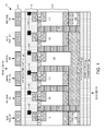
- FIG. 1 is a cross sectional view of an example of a visible and infrared image sensor pixel array 100 (hereinafter "pixel array"), in accordance with the teachings of the present invention.
- Pixel array 100 includes an Si x Ge y layer 109 disposed on a first semiconductor layer 131.
- first semiconductor layer 131 comprises silicon.
- a plurality of pixels e . g . red pixel 161, green pixel 163, IR pixel 165, and blue pixel 167) are disposed proximate to a front side 149 of first semiconductor layer 131.
- the plurality of pixels includes a first portion of pixels each of which includes first doped region 119, which is separated from Si x Ge y layer 109 by a spacer region 111.
- the plurality of pixels also includes a second portion of pixels, with each one of the second portion of pixels having a first doped region 120 in contact with Si x Ge y layer 109 formed proximate to a backside 151 of first semiconductor layer 131.
- the first portion of pixels includes red pixels 161, green pixels 163, and blue pixels 167
- the second portion of pixels includes infrared pixels 165.
- Si x Ge y layer 109 is n-type
- spacer region 111 is p-type
- first doped region 119/120 is n-type.
- the polarity of the layers/regions may be reversed.
- Pixel array 100 may also include pinning wells 113/115 disposed between individual pixels (e.g. red pixel 161, green pixel 163, IR pixel 165, and blue pixel 167).
- a first portion of pinning wells 113 extend through first semiconductor layer 131 and separate individual pixels.
- a second portion of pinning wells 115 extend through first semiconductor layer 131 and through Si x Ge y layer 109.
- second portion of pinning wells 115 separate groups of pixels including at least a red pixel 161, a green pixel 163, a blue pixel 167, and an infrared pixel 165.
- pinning wells 113/115 may include p-type semiconductor.
- pixel array 100 may further include a light filter layer 137, which may include red light filters 123, green light filters 125, blue light filters 129, and infrared light filters 127.
- red light filters 123, green light filters 125, and blue light filters 129 are positioned to transmit visible and infrared light to the first portion of pixels ( e.g . red pixel 161, green pixel 163, and blue pixel 167).
- Infrared light filters 127 are positioned to transmit at least infrared light to the second portion of pixels
- light filter layer 137 may be arranged into a Bayer Pattern, X-Trans Pattern, EXR Pattern, or the like.
- pixel array 100 may also include a capping layer 107, oxide layer 105, and carrier wafer 103.
- capping layer 107 may be formed on second semiconductor layer 109.
- capping layer 107 is a p+ Si capping layer.
- An oxide layer 105 may then be formed on capping layer 107.
- Oxide layer 105 may be used to secure carrier wafer 103 to the existing layers of device architecture (e . g . capping layer 107, second semiconductor layer 109, and first semiconductor layer 131). Carrier wafer 103 allows for processing of remaining device architectures.
- a microlens layer (including individual microlenses) is fabricated proximate to the light filter layer 137.
- the microlens layer is positioned to transmit incident light through light filter layer 137, antireflection coating 135, and isolation layer 133, into the individual pixels.
- Pixel array 100 is capable of detecting both visible and infrared light. As illustrated in the example depicted in FIG. 1 , both visible and IR photons are directed though light filter layer 137, antireflection coating 135, isolation layer 133 and into first semiconductor layer 131.
- first doped region 119/120 is n-type and second doped region 141 is p-type; however, in another example, the polarity of the first doped region 119/120 and second doped region 141 may be reversed.
- Image charge accumulated may be transferred to a floating diffusion 143 by applying a voltage to transfer gate 145. Subsequently, charge may be read out of floating diffusion 143 via conductive interconnects 147.
- Si x Ge y layer 109 has a lower band gap than the silicon that may be used to form first semiconductor layer 131. Accordingly, Si x Ge y layer 109 is capable of absorbing infrared photons more efficiently. Once a photon is absorbed in Si x Ge y layer 109, charge may be transferred into first doped region 120, as first doped region 120 is in contact with Si x Ge y layer 109. A p-n junction is formed at the interface of first doped region 120 and second doped region 141. In one example, first doped region 119/120 is n-type and second doped region 141 is p-type.
- Image charge accumulated may be transferred to a floating diffusion 143 by applying a voltage to transfer gate 145. Subsequently, charge may be read out of floating diffusion 143 via conductive interconnects 147. This image charge may be used to from an infrared image or a hybrid visible-infrared image.
- multiple pixels may share a single floating diffusion 143, including examples with two, four, six, and eight pixels all sharing the same floating diffusion 143.
- each pixel has its own transfer gate 145. Accordingly, charge may be read out of individual pixels one a time by applying a voltage to one transfer gate 145 at a time. Conversely, charge may be read out of multiple pixels at the same time by applying a voltage to several of the transfer gates 145 in unison.
- Si x Ge y layer 109 includes silicon and germanium and is gradated such that germanium content increases in a direction. Large Ge atoms may strain a predominantly silicon lattice. Accordingly, to reduce lattice strain, Ge content is slowly increased in the direction moving away from first semiconductor layer 131.
- Si x Ge y layer 109 may be grown using atomic layer deposition (ALD), chemical vapor deposition (CVD), molecular beam epitaxy (MBE), or the like.
- ALD atomic layer deposition
- CVD chemical vapor deposition
- MBE molecular beam epitaxy
- second Si x Ge y layer 109 may include other elements. For instance, doping Si x Ge y layer 109 with boron, nitrogen, phosphorus, arsenic, or gallium, may introduce different energy levels into the host-material band gap. Electrons can then be knocked off the dopants at energy levels well below the cutoff wavelengths for silicon or germanium, and IR detection at longer wavelengths becomes possible.
- Si x Ge y layer 109 may be replaced entirely with other low band gap semiconductor materials including other silicon based alloys, germanium based alloys, gallium based alloys, or the like in accordance with the teachings of the present invention. These other low bandgap semiconductor materials may also be doped with elements, including, for example, boron, nitrogen, and phosphorus.
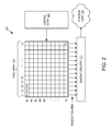
- FIG. 2 is a block diagram illustrating one example of a visible and infrared image sensor 200 (hereinafter "image sensor"), in accordance with the teachings of the present invention.
- image sensor 200 includes pixel array 205, readout circuitry 211, function logic 215, and control circuitry 221.
- pixel array 205 is a two-dimensional (2D) array of individual pixels ( e . g . pixels P1, P2 ..., Pn) including rows ( e . g . rows R1 to Ry.) and columns ( e.g . column C1 to Cx).
- the pixels P1, P2, ..., Pn may be examples of the pixels ( e.g.
- Pixel array 205 may be used to acquire image data of a person, place, object, etc., which can then be used to render a 2D image of the person, place, object, etc.
- image sensor pixel e.g. red pixel 161, green pixel 163, IR pixel 165, and blue pixel 167 in pixel array 205 has acquired its image data or image charge
- image charge is then readout by readout circuitry 211 and transferred to function logic 215.
- Readout circuitry 211 is coupled to readout image data from the individual pixels in pixel array 205, and function logic 215 is coupled to readout circuitry 211 to perform logic operations on the image data.
- readout circuitry 211 may include amplification circuitry, analog-to-digital (ADC) conversion circuitry, or otherwise.
- Function logic 215 may simply store the image data or even manipulate the image data by applying post image effects (e . g . crop, rotate, remove red eye, adjust brightness, adjust contrast, or otherwise).
- readout circuitry 211 may readout a row of image data at a time along readout column lines (illustrated) or may readout the image data using a variety of other techniques (not illustrated), such as a serial readout or a full parallel readout of all pixels simultaneously.
- control circuitry 221 is coupled to pixel array 205 to control operation of the individual pixels (e.g. P1, P2, P3, etc.) in pixel array 205.
- control circuitry 221 may generate a shutter signal for controlling image acquisition.
- the shutter signal is a global shutter signal for simultaneously enabling all pixels within pixel array 205 to simultaneously capture their respective image data during a single acquisition window.
- the shutter signal is a rolling shutter signal such that each row, column, or group of pixels is sequentially enabled during consecutive acquisition windows.
- image acquisition is synchronized with lighting effects such as a flash.
- image sensor 200 may be included in a digital camera, cell phone, laptop computer, or the like. Additionally, image sensor 200 may be coupled to other elements of hardware such as a processor, memory elements, output (USB port, wireless transmitter, HDMI port, etc.), lighting/flash, electrical input (keyboard, touch display, track pad, mouse, microphone, etc.), and/or display. Other elements of hardware may deliver instructions to image sensor 200, extract image data from image sensor 200, or manipulate image data supplied by image sensor 200.
- a processor such as a processor, memory elements, output (USB port, wireless transmitter, HDMI port, etc.), lighting/flash, electrical input (keyboard, touch display, track pad, mouse, microphone, etc.), and/or display.
- Other elements of hardware may deliver instructions to image sensor 200, extract image data from image sensor 200, or manipulate image data supplied by image sensor 200.
- FIG. 3 is a flowchart of a process 300 for forming a visible and infrared image sensor, in accordance with the teachings of the present invention.
- the order in which some or all of the process blocks appear in each process should not be deemed limiting. Rather, one of ordinary skill in the art having the benefit of the present disclosure will understand that some of the process blocks may be executed in a variety of orders not illustrated, or even in parallel.
- Process block 301 shows forming a second semiconductor layer (e . g . Si x Ge y layer 109) on a back side ( e.g. back side 151) of a first semiconductor layer (e.g. first semiconductor layer 131).
- the first semiconductor layer is primarily silicon and the second semiconductor layer includes SiGe.
- the SiGe layer may be doped with other elements, such as born, nitrogen, phosphorus, or the like.
- Ge content in the second semiconductor layer is gradated such that the Ge concentration increases in a direction moving away from the first semiconductor layer. Since the SiGe lattice constant is higher than that of silicon, the SiGe layer may be prone to a higher thread dislocation density if the Ge concentration in the solid solution is increased to rapidly.
- the Ge in the SiGe layer is often increased at no more than 10% Ge per micron (up to a concentration of ⁇ 30% Ge), in order to prevent the formation of thread dislocations. Chemical-mechanical polishing may be used to reduce defects.
- Process block 303 shows forming a capping layer (e.g . p+ Si capping layer 107) disposed proximate to the second semiconductor layer, such that the second semiconductor layer (e.g . Si x Ge y layer 109) is disposed between the first semiconductor layer (e.g. first semiconductor layer 131) and the capping layer.
- the capping layer will likely be strained due to the high Ge content in the back side of the second semiconductor layer (side not in contact with the first semiconductor layer).
- the capping layer should not be limited to just p+ Si, one skilled in the art having the benefit of the present disclosure will recognize that other materials (e.g . other semiconductors/oxides) may be used to achieve the same or a similar result.
- Process block 305 illustrates forming an oxide layer (e.g . bonding oxide 105) on the p+ Si capping layer. Accordingly, the oxide layer is disposed proximate to the second semiconductor layer, and the second semiconductor layer is disposed between the first semiconductor layer and the oxide layer.
- the bonding oxide layer may include a semiconductor oxide or a metal oxide.
- a carrier wafer (e . g . carrier wafer 103) is attached to the oxide layer, this allows for processing of pixel architecture in/on the first semiconductor layer.
- the carrier wafer may include silicon, silicon oxide, metal oxide, or the like.
- Process block 309 shows processing pixels, pinning wells, and supporting architecture in/on the front side ( e.g. front side 149) of the first semiconductor layer.
- this process includes forming one or more groups of pixels (e.g. red pixel 161, green pixel 163, IR pixel 165, and blue pixel 167) disposed in a front side of the first semiconductor layer.
- Forming the one or more groups of pixels may include forming a first and second portion of pixels.
- the first portion of pixels e.g . red pixel 161, green pixel 163, and blue pixel 167) may be separated from the second semiconductor layer by a spacer region ( e.g . spacer region 111).
- the second portion of pixels e.g .
- IR pixel 165) may include a first doped region (e.g. first doped region 120), and the first doped region may be in contact with the second semiconductor layer.
- the first doped region may also be of a same majority charge carrier type as the second semiconductor layer.
- pinning wells may be formed to separate individual pixels in the one or more groups of pixels.
- the pinning wells e.g . pinning wells 113 extend through the first semiconductor layer.
- deep pinning wells e.g . deep pinning wells 115
- the deep pinning wells extend through the first and second semiconductor layers.
- an isolation layer (e.g . isolation layer 133) may be formed proximate to the front side of the first semiconductor layer, and the isolation layer may include conductive interconnects (e.g . conductive interconnects 147).
- the isolation layer may be fabricated from silicon oxide, metal oxide, a polymer, or the like.
- the conductive interconnects may include metal.
- An antireflection coating (e.g . antireflection coating 135) may also be formed such that the isolation layer is disposed between the first semiconductor layer and the antireflection coating.
- a light filter layer (e.g. light filter layer 137) may be formed, and the light filter layer may include red, green, blue and infrared light filters. In one example, the light filter layer is disposed such that the antireflection coating is located between the isolation layer and the light filter layer.
- forming the second semiconductor layer may occur before forming the one or more groups of pixels. However in a different example, forming the second semiconductor layer may occur after forming at least part of the one or more groups of pixels.
- FIGs. 4A-4C show a process 400 of forming a visible and infrared image sensor, in accordance with the teachings of the present invention. It is worth noting that parts of the process 400 correspond to process blocks in process 300. The order in which some or all of the process occurs should not be deemed limiting. Rather, one of ordinary skill in the art having the benefit of the present disclosure will understand that some of the process may be executed in a variety of orders not illustrated, or even in parallel.
- FIG. 4A shows forming a second semiconductor layer 409 on a back side 451 of a first semiconductor layer 431 ( see process block 301).
- the first semiconductor layer 431 is primarily silicon and second semiconductor layer 409 includes SiGe.
- second semiconductor layer 409 also includes doping elements such as boron, nitrogen, phosphorus, or the like.
- the Ge content in second semiconductor layer 409 may be gradated and increase in a direction moving away from first semiconductor layer 431. As previously stated, Ge gradation may help to reduce dislocation density in second semiconductor layer 409.
- FIG. 4B illustrates the construction of several elements of device architecture (e.g . p+ Si capping layer 407, bonding oxide 405, and carrier wafer 403) that may occur before fabricating the majority of pixel device architecture ( see FIG. 4C ).
- a capping layer 407 may be formed on second semiconductor layer 409.
- capping layer 407 is a p+ Si capping layer.
- An oxide layer 405 may then be formed on capping layer 407.
- Oxide layer 405 is used to secure carrier wafer 403 to the existing layers of device architecture (e.g . capping layer 407, second semiconductor layer 409, and first semiconductor layer 431). Carrier wafer 403 allows for processing of remaining device architectures.
- FIG. 4C illustrates the processing of remaining device architecture in/on a front side 449 of the first semiconductor layer 431 ( see process block 309).
- this process includes forming one or more groups of pixels (e.g. red pixel 461, green pixel 463, IR pixel 465, and blue pixel 467) disposed in front side 449 of the first semiconductor layer 431.
- Forming the one or more groups of pixels may include forming a first and second portion of pixels.
- the first portion of pixels e.g. red pixel 461, green pixel 463, and blue pixel 467) are separated from the second semiconductor layer 409 by a spacer region 411.
- the second portion of pixels e.g.
- IR pixel 465) include a first doped region 420 in contact with second semiconductor layer 409.
- First doped region 420 may also be of a same majority charge carrier type as second semiconductor layer 409 ( e.g. both are n-type or both are p-type).
- pinning wells 413 are formed to separate individual pixels in the one or more groups of pixels, wherein pinning wells 413 extend through first semiconductor layer 431.
- deep pinning wells 415 may be formed to separate the one or more groups of pixels, wherein deep pinning wells 415 extend through first semiconductor layer 431 and second semiconductor layer 409.
- an isolation layer 433 may be formed proximate to front side 449 of the first semiconductor layer 431, and isolation layer 433 may include conductive interconnects 447.
- Isolation layer 433 may be fabricated from silicon oxide, metal oxide, a polymer, or the like. Additionally, conductive interconnects 447 may include metal.
- An antireflection coating 435 may also be formed such that isolation layer 433 is disposed between first semiconductor layer 431 and antireflection coating 435.
- Light filter layer 437 may be formed and include a red light filter 423, a green light filter 425, a blue light filter 429, and an infrared light filter 427. In one example, light filter layer 437 is disposed such that antireflection coating 435 is located between isolation layer 433 and light filter layer 437. Although not depicted, light filter layer 437 may be one continuous layer, including individual light filters.
- a microlens layer (including individual microlenses) is fabricated proximate to light filter layer 437.
- the microlenses are positioned to transmit incident light through light filter layer 437, antireflection coating 435, and isolation layer 433, into the individual pixels.
Landscapes
- Solid State Image Pick-Up Elements (AREA)
- Physics & Mathematics (AREA)
- Spectroscopy & Molecular Physics (AREA)
- Transforming Light Signals Into Electric Signals (AREA)
- Light Receiving Elements (AREA)
Abstract
Description
- This disclosure relates generally to image sensors, and in particular but not exclusively, relates to visible and infrared image sensors.
- An image sensor is an electronic device that converts light (in the form of an optical image) into electronic signals. Semiconductor based image sensors have become ubiquitous in modem electronic devices such as cell phones, portable cameras, and desktop/laptop computers. Modem image sensors are generally semiconductor charge-coupled devices (CCD), active pixel sensors in complementary metal-oxide-semiconductor (CMOS), or N-type metal-oxide-semiconductor (NMOS) technologies. Typically these devices are used to capture visible light; however, in certain applications detection of light outside of the visible spectrum is desirable.
- Infrared (IR) light is one part of the electromagnetic spectrum. All objects emit some amount of black body radiation as a function of their temperature. Generally, the higher the object's temperature, the more IR light is emitted as black-body radiation. An image sensor made to detect IR works even in total darkness because no ambient light is required. Accordingly, an IR image sensor may be helpful in rescue operations, night time photography, and other dark conditions.
- Even more useful than an image sensor that can only detect infrared light, is an image sensor that can detect both IR and visible light. However, detection of infrared light generally requires low-band gap materials that are difficult to integrate with traditional image sensor fabrication processes. Accordingly, it has proved challenging to merge infrared and visible imaging technologies. This difficulty in fabricating hybrid visible-IR image sensors has resulted in hybrid sensors that suffer from low IR sensitivity, visible light contamination, semiconductor defects, and the like.
- Non-limiting and non-exhaustive examples of the invention are described with reference to the following figures, wherein like reference numerals refer to like parts throughout the various views unless otherwise specified.
-
FIG. 1 is a cross sectional view of an example of a visible and infrared image sensor pixel array, in accordance with the teachings of the present invention. -
FIG. 2 is a block diagram illustrating one example of a visible and infrared image sensor, in accordance with the teachings of the present invention. -
FIG. 3 is a flowchart of a process for forming a visible and infrared image sensor, in accordance with the teachings of the present invention. -
FIGs. 4A-4C show a process for forming a visible and infrared image sensor, in accordance with the teachings of the present invention. - Examples of a system and method for forming a visible and infrared (hereinafter "IR") image sensor are described herein. In the following description, numerous specific details are set forth to provide a thorough understanding of the examples. One skilled in the relevant art, having the benefit of the present disclosure will recognize, however, that the techniques described herein can be practiced without one or more of the specific details, or with other methods, components, materials, etc. In other instances, well-known structures, materials, or operations are not shown or described in detail to avoid obscuring certain aspects.
- Reference throughout this specification to "one example" or "one embodiment" means that a particular feature, structure, or characteristic described in connection with the example is included in at least one embodiment of the present invention. Thus, the appearances of the phrases "in one example" or "in one embodiment" in various places throughout this specification are not necessarily all referring to the same embodiment. Furthermore, the particular features, structures, or characteristics may be combined in any suitable manner in one or more examples.
- Throughout this specification, several terms of art are used. These terms are to take on their ordinary meaning in the art from which they come, unless specifically defined herein or the context of their use would clearly suggest otherwise. It should be noted that elements and compounds are referred to by their proper name or elemental symbol interchangeably (e.g. silicon vs. Si).
-
FIG. 1 is a cross sectional view of an example of a visible and infrared image sensor pixel array 100 (hereinafter "pixel array"), in accordance with the teachings of the present invention.Pixel array 100 includes an SixGeylayer 109 disposed on afirst semiconductor layer 131. In one example,first semiconductor layer 131 comprises silicon. A plurality of pixels (e.g.red pixel 161,green pixel 163,IR pixel 165, and blue pixel 167) are disposed proximate to afront side 149 offirst semiconductor layer 131. The plurality of pixels includes a first portion of pixels each of which includes firstdoped region 119, which is separated from SixGeylayer 109 by aspacer region 111. The plurality of pixels also includes a second portion of pixels, with each one of the second portion of pixels having a firstdoped region 120 in contact with SixGeylayer 109 formed proximate to abackside 151 offirst semiconductor layer 131. In one example, the first portion of pixels includesred pixels 161,green pixels 163, andblue pixels 167, and the second portion of pixels includesinfrared pixels 165. In one example, SixGeylayer 109 is n-type,spacer region 111 is p-type, and first dopedregion 119/120 is n-type. However, in another example, the polarity of the layers/regions may be reversed. -
Pixel array 100 may also includepinning wells 113/115 disposed between individual pixels (e.g.red pixel 161,green pixel 163,IR pixel 165, and blue pixel 167). A first portion ofpinning wells 113 extend throughfirst semiconductor layer 131 and separate individual pixels. A second portion ofpinning wells 115 extend throughfirst semiconductor layer 131 and through SixGeylayer 109. In one example, second portion ofpinning wells 115 separate groups of pixels including at least ared pixel 161, agreen pixel 163, ablue pixel 167, and aninfrared pixel 165. In another or the same example, pinningwells 113/115 may include p-type semiconductor. - In one example,
pixel array 100 may further include alight filter layer 137, which may includered light filters 123,green light filters 125,blue light filters 129, andinfrared light filters 127. In one example,red light filters 123,green light filters 125, andblue light filters 129 are positioned to transmit visible and infrared light to the first portion of pixels (e.g.red pixel 161,green pixel 163, and blue pixel 167).Infrared light filters 127 are positioned to transmit at least infrared light to the second portion of pixels - (e.g. IR pixel 165). Additionally,
light filter layer 137 may be arranged into a Bayer Pattern, X-Trans Pattern, EXR Pattern, or the like. - In one example,
pixel array 100 may also include acapping layer 107, oxide layer 105, and carrier wafer 103. After formingsecond semiconductor layer 109,capping layer 107 may be formed onsecond semiconductor layer 109. In one example,capping layer 107 is a p+ Si capping layer. An oxide layer 105 may then be formed oncapping layer 107. Oxide layer 105 may be used to secure carrier wafer 103 to the existing layers of device architecture (e.g.capping layer 107,second semiconductor layer 109, and first semiconductor layer 131). Carrier wafer 103 allows for processing of remaining device architectures. - It should be noted that other elements of optical device architecture may also be formed that are not depicted. In one example, a microlens layer (including individual microlenses) is fabricated proximate to the
light filter layer 137. The microlens layer is positioned to transmit incident light throughlight filter layer 137,antireflection coating 135, andisolation layer 133, into the individual pixels. -
Pixel array 100 is capable of detecting both visible and infrared light. As illustrated in the example depicted inFIG. 1 , both visible and IR photons are directed thoughlight filter layer 137,antireflection coating 135,isolation layer 133 and intofirst semiconductor layer 131. - Visible light is absorbed in
first semiconductor layer 131 generating charge in firstdoped region 119/120. A p-n junction is formed at the interface of firstdoped region 119/120 and seconddoped region 141. In one example, firstdoped region 119/120 is n-type and seconddoped region 141 is p-type; however, in another example, the polarity of the firstdoped region 119/120 and seconddoped region 141 may be reversed. Image charge accumulated may be transferred to a floatingdiffusion 143 by applying a voltage to transfergate 145. Subsequently, charge may be read out of floatingdiffusion 143 viaconductive interconnects 147. - Conversely, IR light passes through
first semiconductor layer 131 and into SixGey layer 109. SixGey layer 109 has a lower band gap than the silicon that may be used to formfirst semiconductor layer 131. Accordingly, SixGey layer 109 is capable of absorbing infrared photons more efficiently. Once a photon is absorbed in SixGey layer 109, charge may be transferred into firstdoped region 120, as firstdoped region 120 is in contact with SixGey layer 109. A p-n junction is formed at the interface of firstdoped region 120 and seconddoped region 141. In one example, firstdoped region 119/120 is n-type and seconddoped region 141 is p-type. Image charge accumulated may be transferred to a floatingdiffusion 143 by applying a voltage to transfergate 145. Subsequently, charge may be read out of floatingdiffusion 143 viaconductive interconnects 147. This image charge may be used to from an infrared image or a hybrid visible-infrared image. - It should be noted that in other examples (not depicted), multiple pixels may share a single floating
diffusion 143, including examples with two, four, six, and eight pixels all sharing the same floatingdiffusion 143. In examples with multiple pixels sharing the same floatingdiffusion 143, each pixel has itsown transfer gate 145. Accordingly, charge may be read out of individual pixels one a time by applying a voltage to onetransfer gate 145 at a time. Conversely, charge may be read out of multiple pixels at the same time by applying a voltage to several of thetransfer gates 145 in unison. - In one example, SixGey layer 109 includes silicon and germanium and is gradated such that germanium content increases in a direction. Large Ge atoms may strain a predominantly silicon lattice. Accordingly, to reduce lattice strain, Ge content is slowly increased in the direction moving away from
first semiconductor layer 131. In order to achieve the gradated structure of SixGey layer 109, SixGey layer 109 may be grown using atomic layer deposition (ALD), chemical vapor deposition (CVD), molecular beam epitaxy (MBE), or the like. The incorporation of gradated SixGey layer 109 intopixel array 100 allows for a highly sensitive IR absorption layer to be uniformly integrated into a visible and IR image sensor. This results in the formation of hybrid image sensor with superior performance and enhanced versatility of use over conventional IR imaging systems. - In one example, second SixGey layer 109 may include other elements. For instance, doping SixGey layer 109 with boron, nitrogen, phosphorus, arsenic, or gallium, may introduce different energy levels into the host-material band gap. Electrons can then be knocked off the dopants at energy levels well below the cutoff wavelengths for silicon or germanium, and IR detection at longer wavelengths becomes possible. In another example, SixGey layer 109 may be replaced entirely with other low band gap semiconductor materials including other silicon based alloys, germanium based alloys, gallium based alloys, or the like in accordance with the teachings of the present invention. These other low bandgap semiconductor materials may also be doped with elements, including, for example, boron, nitrogen, and phosphorus.
-
FIG. 2 is a block diagram illustrating one example of a visible and infrared image sensor 200 (hereinafter "image sensor"), in accordance with the teachings of the present invention. As shown in the depicted example,image sensor 200 includespixel array 205,readout circuitry 211,function logic 215, andcontrol circuitry 221. In one example,pixel array 205 is a two-dimensional (2D) array of individual pixels (e.g. pixels P1, P2 ..., Pn) including rows (e.g. rows R1 to Ry.) and columns (e.g. column C1 to Cx). In one example, it is appreciated that the pixels P1, P2, ..., Pn may be examples of the pixels (e.g.red pixel 161,green pixel 163,IR pixel 165, and blue pixel 167) included inpixel array 100 discussed inFIG. 1 .Pixel array 205 may be used to acquire image data of a person, place, object, etc., which can then be used to render a 2D image of the person, place, object, etc. In one example, after each image sensor pixel (e.g.red pixel 161,green pixel 163,IR pixel 165, and blue pixel 167) inpixel array 205 has acquired its image data or image charge, image charge is then readout byreadout circuitry 211 and transferred to functionlogic 215.Readout circuitry 211 is coupled to readout image data from the individual pixels inpixel array 205, andfunction logic 215 is coupled toreadout circuitry 211 to perform logic operations on the image data. In various examples,readout circuitry 211 may include amplification circuitry, analog-to-digital (ADC) conversion circuitry, or otherwise.Function logic 215 may simply store the image data or even manipulate the image data by applying post image effects (e.g. crop, rotate, remove red eye, adjust brightness, adjust contrast, or otherwise). In one example,readout circuitry 211 may readout a row of image data at a time along readout column lines (illustrated) or may readout the image data using a variety of other techniques (not illustrated), such as a serial readout or a full parallel readout of all pixels simultaneously. - In one example,
control circuitry 221 is coupled topixel array 205 to control operation of the individual pixels (e.g. P1, P2, P3, etc.) inpixel array 205. For example,control circuitry 221 may generate a shutter signal for controlling image acquisition. In one example, the shutter signal is a global shutter signal for simultaneously enabling all pixels withinpixel array 205 to simultaneously capture their respective image data during a single acquisition window. In another example, the shutter signal is a rolling shutter signal such that each row, column, or group of pixels is sequentially enabled during consecutive acquisition windows. In another example, image acquisition is synchronized with lighting effects such as a flash. - In one example,
image sensor 200 may be included in a digital camera, cell phone, laptop computer, or the like. Additionally,image sensor 200 may be coupled to other elements of hardware such as a processor, memory elements, output (USB port, wireless transmitter, HDMI port, etc.), lighting/flash, electrical input (keyboard, touch display, track pad, mouse, microphone, etc.), and/or display. Other elements of hardware may deliver instructions toimage sensor 200, extract image data fromimage sensor 200, or manipulate image data supplied byimage sensor 200. -
FIG. 3 is a flowchart of aprocess 300 for forming a visible and infrared image sensor, in accordance with the teachings of the present invention. The order in which some or all of the process blocks appear in each process should not be deemed limiting. Rather, one of ordinary skill in the art having the benefit of the present disclosure will understand that some of the process blocks may be executed in a variety of orders not illustrated, or even in parallel. -
Process block 301 shows forming a second semiconductor layer (e.g. SixGey layer 109) on a back side (e.g. back side 151) of a first semiconductor layer (e.g. first semiconductor layer 131). In one example, the first semiconductor layer is primarily silicon and the second semiconductor layer includes SiGe. The SiGe layer may be doped with other elements, such as born, nitrogen, phosphorus, or the like. Sometimes Ge content in the second semiconductor layer is gradated such that the Ge concentration increases in a direction moving away from the first semiconductor layer. Since the SiGe lattice constant is higher than that of silicon, the SiGe layer may be prone to a higher thread dislocation density if the Ge concentration in the solid solution is increased to rapidly. The Ge in the SiGe layer is often increased at no more than 10% Ge per micron (up to a concentration of ∼30% Ge), in order to prevent the formation of thread dislocations. Chemical-mechanical polishing may be used to reduce defects. -
Process block 303 shows forming a capping layer (e.g. p+ Si capping layer 107) disposed proximate to the second semiconductor layer, such that the second semiconductor layer (e.g. SixGey layer 109) is disposed between the first semiconductor layer (e.g. first semiconductor layer 131) and the capping layer. The capping layer will likely be strained due to the high Ge content in the back side of the second semiconductor layer (side not in contact with the first semiconductor layer). The capping layer should not be limited to just p+ Si, one skilled in the art having the benefit of the present disclosure will recognize that other materials (e.g. other semiconductors/oxides) may be used to achieve the same or a similar result. -
Process block 305 illustrates forming an oxide layer (e.g. bonding oxide 105) on the p+ Si capping layer. Accordingly, the oxide layer is disposed proximate to the second semiconductor layer, and the second semiconductor layer is disposed between the first semiconductor layer and the oxide layer. In one example, the bonding oxide layer may include a semiconductor oxide or a metal oxide. - In
process block 307, a carrier wafer (e.g. carrier wafer 103) is attached to the oxide layer, this allows for processing of pixel architecture in/on the first semiconductor layer. The carrier wafer may include silicon, silicon oxide, metal oxide, or the like. -
Process block 309 shows processing pixels, pinning wells, and supporting architecture in/on the front side (e.g. front side 149) of the first semiconductor layer. In one example, this process includes forming one or more groups of pixels (e.g.red pixel 161,green pixel 163,IR pixel 165, and blue pixel 167) disposed in a front side of the first semiconductor layer. Forming the one or more groups of pixels may include forming a first and second portion of pixels. The first portion of pixels (e.g.red pixel 161,green pixel 163, and blue pixel 167) may be separated from the second semiconductor layer by a spacer region (e.g. spacer region 111). The second portion of pixels (e.g. IR pixel 165) may include a first doped region (e.g. first doped region 120), and the first doped region may be in contact with the second semiconductor layer. The first doped region may also be of a same majority charge carrier type as the second semiconductor layer. - Additionally, pinning wells may be formed to separate individual pixels in the one or more groups of pixels. The pinning wells (e.g. pinning wells 113) extend through the first semiconductor layer. Similarly, deep pinning wells (e.g. deep pinning wells 115) may be formed to separate the one or more groups of pixels, wherein the deep pinning wells extend through the first and second semiconductor layers.
- In one example, an isolation layer (e.g. isolation layer 133) may be formed proximate to the front side of the first semiconductor layer, and the isolation layer may include conductive interconnects (e.g. conductive interconnects 147). The isolation layer may be fabricated from silicon oxide, metal oxide, a polymer, or the like. The conductive interconnects may include metal. An antireflection coating (e.g. antireflection coating 135) may also be formed such that the isolation layer is disposed between the first semiconductor layer and the antireflection coating. Additionally, a light filter layer (e.g. light filter layer 137) may be formed, and the light filter layer may include red, green, blue and infrared light filters. In one example, the light filter layer is disposed such that the antireflection coating is located between the isolation layer and the light filter layer.
- As illustrated in
FIG. 3 , forming the second semiconductor layer may occur before forming the one or more groups of pixels. However in a different example, forming the second semiconductor layer may occur after forming at least part of the one or more groups of pixels. -
FIGs. 4A-4C show aprocess 400 of forming a visible and infrared image sensor, in accordance with the teachings of the present invention. It is worth noting that parts of theprocess 400 correspond to process blocks inprocess 300. The order in which some or all of the process occurs should not be deemed limiting. Rather, one of ordinary skill in the art having the benefit of the present disclosure will understand that some of the process may be executed in a variety of orders not illustrated, or even in parallel. -
FIG. 4A shows forming asecond semiconductor layer 409 on aback side 451 of a first semiconductor layer 431 (see process block 301). In one example, thefirst semiconductor layer 431 is primarily silicon andsecond semiconductor layer 409 includes SiGe. In one example,second semiconductor layer 409 also includes doping elements such as boron, nitrogen, phosphorus, or the like. The Ge content insecond semiconductor layer 409 may be gradated and increase in a direction moving away fromfirst semiconductor layer 431. As previously stated, Ge gradation may help to reduce dislocation density insecond semiconductor layer 409. -
FIG. 4B illustrates the construction of several elements of device architecture (e.g. p+Si capping layer 407,bonding oxide 405, and carrier wafer 403) that may occur before fabricating the majority of pixel device architecture (seeFIG. 4C ). After formingsecond semiconductor layer 409, acapping layer 407 may be formed onsecond semiconductor layer 409. In one example, cappinglayer 407 is a p+ Si capping layer. Anoxide layer 405 may then be formed on cappinglayer 407.Oxide layer 405 is used to securecarrier wafer 403 to the existing layers of device architecture (e.g. cappinglayer 407,second semiconductor layer 409, and first semiconductor layer 431).Carrier wafer 403 allows for processing of remaining device architectures. -
FIG. 4C illustrates the processing of remaining device architecture in/on afront side 449 of the first semiconductor layer 431 (see process block 309). In one example, this process includes forming one or more groups of pixels (e.g.red pixel 461,green pixel 463,IR pixel 465, and blue pixel 467) disposed infront side 449 of thefirst semiconductor layer 431. Forming the one or more groups of pixels may include forming a first and second portion of pixels. The first portion of pixels (e.g.red pixel 461,green pixel 463, and blue pixel 467) are separated from thesecond semiconductor layer 409 by aspacer region 411. The second portion of pixels (e.g. IR pixel 465) include a firstdoped region 420 in contact withsecond semiconductor layer 409. First dopedregion 420 may also be of a same majority charge carrier type as second semiconductor layer 409 (e.g. both are n-type or both are p-type). - In one example, pinning
wells 413 are formed to separate individual pixels in the one or more groups of pixels, wherein pinningwells 413 extend throughfirst semiconductor layer 431. Similarly, deep pinningwells 415 may be formed to separate the one or more groups of pixels, wherein deep pinningwells 415 extend throughfirst semiconductor layer 431 andsecond semiconductor layer 409. - In one example, an
isolation layer 433 may be formed proximate tofront side 449 of thefirst semiconductor layer 431, andisolation layer 433 may includeconductive interconnects 447.Isolation layer 433 may be fabricated from silicon oxide, metal oxide, a polymer, or the like. Additionally,conductive interconnects 447 may include metal. Anantireflection coating 435 may also be formed such thatisolation layer 433 is disposed betweenfirst semiconductor layer 431 andantireflection coating 435.Light filter layer 437 may be formed and include ared light filter 423, agreen light filter 425, a bluelight filter 429, and an infraredlight filter 427. In one example,light filter layer 437 is disposed such thatantireflection coating 435 is located betweenisolation layer 433 andlight filter layer 437. Although not depicted,light filter layer 437 may be one continuous layer, including individual light filters. - Other elements of device architecture may also be formed that are not depicted. In one example, a microlens layer (including individual microlenses) is fabricated proximate to
light filter layer 437. The microlenses are positioned to transmit incident light throughlight filter layer 437,antireflection coating 435, andisolation layer 433, into the individual pixels. - The above description of illustrated examples of the invention, including what is described in the Abstract, is not intended to be exhaustive or to limit the invention to the precise forms disclosed. While specific examples of, and examples for, the invention are described herein for illustrative purposes, various modifications are possible within the scope of the invention, as those skilled in the relevant art will recognize.
- These modifications can be made to the invention in light of the above detailed description. The terms used in the following claims should not be construed to limit the invention to the specific examples disclosed in the specification. Rather, the scope of the invention is to be determined entirely by the following claims, which are to be construed in accordance with established doctrines of claim interpretation.
- The following statements provide general expressions of the disclosure herein.
- A. A pixel array, the pixel array comprising: an SixGey layer disposed on a first semiconductor layer; a plurality of pixels disposed in the first semiconductor layer, the plurality of pixels including: (1) a first portion of pixels, wherein the first portion of pixels are separated from the SixGey layer by a spacer region; and (2) a second portion of pixels, wherein each one of the second portion of pixels includes a first doped region in contact with the SixGey layer; and pinning wells disposed between individual pixels in the plurality of pixels, wherein a first portion of the pinning wells extend through the first semiconductor layer, and a second portion of the pinning wells extend through the first semiconductor layer and the SixGey layer.
- B. The pixel array of statement A, wherein the SixGey layer is gradated such that Ge content increases in a direction.
- C. The pixel array of statement A, wherein the first portion of pixels includes red pixels, green pixels, and blue pixels, and wherein the second portion of pixels includes infrared pixels.
- D. The pixel array of statement C, wherein the second portion of pinning wells separate groups of pixels including at least a red pixel, a green pixel, a blue pixel, and an infrared pixel.
- E. The pixel array of statement A, wherein the SixGey layer comprises silicon and germanium.
- F. The pixel array of statement A, further comprising red, green, blue, and infrared light filters, wherein the red, green, and blue light filters are positioned to transmit visible and infrared light to the first portion of pixels, and wherein the infrared light filters are positioned to transmit at least one of visible and infrared light to the second portion of pixels.
- G. An image sensor, the image sensor comprising: a second semiconductor layer disposed on a back side of a first semiconductor layer; one or more groups of pixels disposed in a front side of the first semiconductor layer, the one or more groups of pixels including: a first portion of pixels, wherein the first portion of pixels are separated from the second semiconductor layer by a spacer region; a second portion of pixels, wherein a first doped region of the second portion of pixels is in contact with the second semiconductor layer, and wherein the first doped region is of a same majority charge carrier type as the second semiconductor layer; pinning wells separating individual pixels in the groups of pixels, wherein the pinning wells extend through the first semiconductor layer; and deep pinning wells separating the one or more groups of pixels, wherein the deep pinning wells extend through the first and second semiconductor layers.
- H. The image sensor of statement G, wherein the second semiconductor layer includes SiGe.
- I. The image sensor of statement G, wherein the first portion of pixels include red pixels, green pixels, and blue pixels, and wherein the second portion of pixels include infrared pixels.
- J. The image sensor of statement I, wherein the one or more groups of pixels include at least a red pixel, a green pixel, a blue pixel, and an infrared pixel.
- K. The image sensor of statement G, wherein each one of the individual pixels include a transfer gate coupled to transfer charge from a second doped region to a floating diffusion, wherein the second doped region is in contact with the first doped region and is of an opposite majority charge carrier type as the first doped region.
- L. The image sensor of statement G, wherein the individual pixels are arranged into a pixel array comprising rows and columns.
- M. The image sensor of statement G, further comprising: control circuitry coupled to control operation of the individual pixels; readout circuitry coupled to readout image data from the individual pixels; and function logic coupled to the readout circuitry to perform logic operations on the image data.
- N. A method of image sensor fabrication, the method comprising: forming a second semiconductor layer on a back side of a first semiconductor layer; forming one or more groups of pixels disposed in a front side of the first semiconductor layer, the one or more groups of pixels including: a first portion of pixels, wherein the first portion of pixels are separated from the second semiconductor layer by a spacer region; a second portion of pixels, wherein a first doped region of the second portion of pixels is in contact with the second semiconductor layer, and wherein the first doped region is of a same majority charge carrier type as the second semiconductor layer; pinning wells separating individual pixels in the one or more groups of pixels, wherein the pinning wells extend through the first semiconductor layer; and deep pinning wells separating the one or more groups of pixels, wherein the deep pinning wells extend through the first and second semiconductor layers.
- O. The method of statement N, wherein forming the second semiconductor layer comprises forming a layer including SiGe, wherein Ge content increases in a direction.
- P. The method of statement N, further comprising forming a capping layer disposed proximate to the second semiconductor layer, wherein the second semiconductor layer is disposed between the first semiconductor layer and the capping layer.
- Q. The method of statement N, further comprising forming an oxide layer disposed proximate to the second semiconductor layer, wherein the second semiconductor layer is disposed between the first semiconductor layer and the oxide layer.
- R. The method of statement Q further comprising attaching a carrier wafer to the oxide layer.
- S. The method of statement N, wherein forming the second semiconductor layer occurs before forming the one or more groups of pixels.
- T. The method of statement N, wherein forming the second semiconductor layer occurs after forming at least part of the one or more groups of pixels.
- U. The method of statement N, further comprising: forming an isolation layer disposed proximate to the front side of the first semiconductor layer, wherein the isolation layer includes conductive interconnects; forming an antireflection coating, wherein the isolation layer is disposed between the first semiconductor layer and the antireflection coating; and forming a light filter layer, wherein the light filter layer includes red, green, blue and infrared light filters, and wherein the antireflection coating is disposed between the isolation layer and the light filter layer.
Claims (15)
- A pixel array, the pixel array comprising:an SixGey layer disposed on a first semiconductor layer;a plurality of pixels disposed in the first semiconductor layer, the plurality of pixels including:(1) a first portion of pixels, wherein the first portion of pixels are separated from the SixGey layer by a spacer region; and(2) a second portion of pixels, wherein each one of the second portion of pixels includes a first doped region in contact with the SixGey layer; andpinning wells disposed between individual pixels in the plurality of pixels, wherein a first portion of the pinning wells extend through the first semiconductor layer, and a second portion of the pinning wells extend through the first semiconductor layer and the SixGey layer.
- The pixel array of claim 1, wherein the SixGey layer is gradated such that Ge content increases in a direction.
- The pixel array of claim 1, wherein the first portion of pixels includes red pixels, green pixels, and blue pixels, and wherein the second portion of pixels includes infrared pixels, wherein optionally the second portion of pinning wells separate groups of pixels including at least a red pixel, a green pixel, a blue pixel, and an infrared pixel.
- The pixel array of claim 1, further comprising red, green, blue, and infrared light filters, wherein the red, green, and blue light filters are positioned to transmit visible and infrared light to the first portion of pixels, and wherein the infrared light filters are positioned to transmit at least one of visible and infrared light to the second portion of pixels.
- An image sensor, the image sensor comprising:a second semiconductor layer disposed on a back side of a first semiconductor layer;one or more groups of pixels disposed in a front side of the first semiconductor layer, the one or more groups of pixels including:a first portion of pixels, wherein the first portion of pixels are separated from the second semiconductor layer by a spacer region;a second portion of pixels, wherein a first doped region of the second portion of pixels is in contact with the second semiconductor layer, and wherein the first doped region is of a same majority charge carrier type as the second semiconductor layer;pinning wells separating individual pixels in the groups of pixels, wherein the pinning wells extend through the first semiconductor layer; anddeep pinning wells separating the one or more groups of pixels, wherein the deep pinning wells extend through the first and second semiconductor layers.
- The image sensor of claim 5, wherein the second semiconductor layer includes SiGe.
- The image sensor of claim 5, wherein the first portion of pixels include red pixels, green pixels, and blue pixels, and wherein the second portion of pixels include infrared pixels, wherein optionally the one or more groups of pixels include at least a red pixel, a green pixel, a blue pixel, and an infrared pixel.
- The image sensor of claim 5, wherein:each one of the individual pixels include a transfer gate coupled to transfer charge from a second doped region to a floating diffusion, wherein the second doped region is in contact with the first doped region and is of an opposite majority charge carrier type as the first doped region; orthe individual pixels are arranged into a pixel array comprising rows and columns.
- The image sensor of claim 5, further comprising:control circuitry coupled to control operation of the individual pixels;readout circuitry coupled to readout image data from the individual pixels; andfunction logic coupled to the readout circuitry to perform logic operations on the image data.
- A method of image sensor fabrication, the method comprising:forming a second semiconductor layer on a back side of a first semiconductor layer;forming one or more groups of pixels disposed in a front side of the first semiconductor layer, the one or more groups of pixels including:a first portion of pixels, wherein the first portion of pixels are separated from the second semiconductor layer by a spacer region;a second portion of pixels, wherein a first doped region of the second portion of pixels is in contact with the second semiconductor layer, and wherein the first doped region is of a same majority charge carrier type as the second semiconductor layer;pinning wells separating individual pixels in the one or more groups of pixels, wherein the pinning wells extend through the first semiconductor layer; anddeep pinning wells separating the one or more groups of pixels, wherein the deep pinning wells extend through the first and second semiconductor layers.
- The method of claim 10, wherein forming the second semiconductor layer comprises forming a layer including SiGe, wherein Ge content increases in a direction.
- The method of claim 10, further comprising:forming a capping layer disposed proximate to the second semiconductor layer, wherein the second semiconductor layer is disposed between the first semiconductor layer and the capping layer; orforming an oxide layer disposed proximate to the second semiconductor layer, wherein the second semiconductor layer is disposed between the first semiconductor layer and the oxide layer, wherein the method optionally further comprises attaching a carrier wafer to the oxide layer.
- The method of claim 10, wherein forming the second semiconductor layer occurs before forming the one or more groups of pixels.
- The method of claim 10, wherein forming the second semiconductor layer occurs after forming at least part of the one or more groups of pixels.
- The method of claim 10, further comprising:forming an isolation layer disposed proximate to the front side of the first semiconductor layer, wherein the isolation layer includes conductive interconnects;forming an antireflection coating, wherein the isolation layer is disposed between the first semiconductor layer and the antireflection coating; andforming a light filter layer, wherein the light filter layer includes red, green, blue and infrared light filters, and wherein the antireflection coating is disposed between the isolation layer and the light filter layer.
Applications Claiming Priority (1)
| Application Number | Priority Date | Filing Date | Title |
|---|---|---|---|
| US14/341,257 US9806122B2 (en) | 2014-07-25 | 2014-07-25 | Visible and infrared image sensor |
Publications (3)
| Publication Number | Publication Date |
|---|---|
| EP2978022A2 true EP2978022A2 (en) | 2016-01-27 |
| EP2978022A3 EP2978022A3 (en) | 2016-08-24 |
| EP2978022B1 EP2978022B1 (en) | 2019-01-09 |
Family
ID=53785438
Family Applications (1)
| Application Number | Title | Priority Date | Filing Date |
|---|---|---|---|
| EP15177089.8A Active EP2978022B1 (en) | 2014-07-25 | 2015-07-16 | Visible and infrared image sensor |
Country Status (4)
| Country | Link |
|---|---|
| US (2) | US9806122B2 (en) |
| EP (1) | EP2978022B1 (en) |
| CN (1) | CN105321966B (en) |
| TW (1) | TWI593092B (en) |
Cited By (1)
| Publication number | Priority date | Publication date | Assignee | Title |
|---|---|---|---|---|
| US20230067395A1 (en) * | 2021-08-30 | 2023-03-02 | Taiwan Semiconductor Manufacturing Company, Ltd. | Pixel array including octagon pixel sensors |
Families Citing this family (32)
| Publication number | Priority date | Publication date | Assignee | Title |
|---|---|---|---|---|
| TWI694604B (en) | 2015-07-23 | 2020-05-21 | 光澄科技股份有限公司 | Light detector |
| EP3370259B1 (en) | 2015-08-04 | 2020-03-11 | Artilux Inc. | Germanium-silicon light sensing apparatus |
| US10707260B2 (en) | 2015-08-04 | 2020-07-07 | Artilux, Inc. | Circuit for operating a multi-gate VIS/IR photodiode |
| US10861888B2 (en) | 2015-08-04 | 2020-12-08 | Artilux, Inc. | Silicon germanium imager with photodiode in trench |
| US10761599B2 (en) | 2015-08-04 | 2020-09-01 | Artilux, Inc. | Eye gesture tracking |
| CN115824395B (en) | 2015-08-27 | 2023-08-15 | 光程研创股份有限公司 | Wide Spectrum Optical Sensor |
| US10741598B2 (en) | 2015-11-06 | 2020-08-11 | Atrilux, Inc. | High-speed light sensing apparatus II |
| US10254389B2 (en) | 2015-11-06 | 2019-04-09 | Artilux Corporation | High-speed light sensing apparatus |
| US10418407B2 (en) | 2015-11-06 | 2019-09-17 | Artilux, Inc. | High-speed light sensing apparatus III |
| US10886309B2 (en) | 2015-11-06 | 2021-01-05 | Artilux, Inc. | High-speed light sensing apparatus II |
| US10739443B2 (en) | 2015-11-06 | 2020-08-11 | Artilux, Inc. | High-speed light sensing apparatus II |
| US9859325B2 (en) * | 2015-11-13 | 2018-01-02 | Taiwan Semiconductor Manufacturing Co., Ltd. | Complementary metal-oxide-semiconductor (CMOS) image sensor with silicon and silicon germanium |
| US9871067B2 (en) | 2015-11-17 | 2018-01-16 | Taiwan Semiconductor Manufacturing Co., Ltd. | Infrared image sensor component |
| JP6814748B2 (en) * | 2016-01-15 | 2021-01-20 | タワー パートナーズ セミコンダクター株式会社 | Solid-state image sensor |
| TWI741934B (en) * | 2016-02-12 | 2021-10-01 | 光程研創股份有限公司 | Optical apparatus, optical system, time-of-flight system and three-dimensional imaging system |
| US10638054B2 (en) * | 2017-01-25 | 2020-04-28 | Cista System Corp. | System and method for visible and infrared high dynamic range sensing |
| KR102604687B1 (en) | 2017-02-01 | 2023-11-20 | 삼성전자주식회사 | Image sensor and Method for fabricating the same |
| US10090347B1 (en) | 2017-05-24 | 2018-10-02 | Semiconductor Components Industries, Llc | Image sensor with near-infrared and visible light pixels |
| DE102017120499A1 (en) * | 2017-05-29 | 2018-11-29 | Friedrich-Schiller-Universität Jena | Radiation detecting semiconductor device |
| TWI630556B (en) * | 2017-07-26 | 2018-07-21 | 聚晶半導體股份有限公司 | Image pick-up apparatus and infrared ray sensing method thereof |
| JP6975341B2 (en) | 2018-02-23 | 2021-12-01 | アーティラックス・インコーポレイテッド | Photodetector and its light detection method |
| US11105928B2 (en) | 2018-02-23 | 2021-08-31 | Artilux, Inc. | Light-sensing apparatus and light-sensing method thereof |
| CN114335030A (en) | 2018-04-08 | 2022-04-12 | 奥特逻科公司 | Optical detection device |
| US10854770B2 (en) | 2018-05-07 | 2020-12-01 | Artilux, Inc. | Avalanche photo-transistor |
| US10969877B2 (en) | 2018-05-08 | 2021-04-06 | Artilux, Inc. | Display apparatus |
| JP7271127B2 (en) * | 2018-10-19 | 2023-05-11 | キヤノン株式会社 | Photoelectric conversion device |
| US11329085B2 (en) * | 2019-08-22 | 2022-05-10 | Omivision Technologies, Inc. | Pixel array with isolated pixels |
| KR20210060734A (en) * | 2019-11-18 | 2021-05-27 | 삼성디스플레이 주식회사 | Electronic apparatus including the optical sensor and method of the manufacturing the same |
| US11626442B2 (en) * | 2020-08-10 | 2023-04-11 | Taiwan Semiconductor Manufacturing Company, Ltd. | Methods for forming image sensors |
| CN115332274B (en) | 2021-05-10 | 2026-01-02 | 联华电子股份有限公司 | Image sensor |
| US12262562B2 (en) * | 2021-08-31 | 2025-03-25 | Omnivision Technologies, Inc. | Image sensor with varying depth deep trench isolation structure for reduced crosstalk |
| CN114038867B (en) * | 2021-11-03 | 2024-08-30 | 云南昆物新跃光电科技有限公司 | InGaAs short wave infrared detector chip for realizing color imaging and preparation thereof |
Family Cites Families (15)
| Publication number | Priority date | Publication date | Assignee | Title |
|---|---|---|---|---|
| US5453611A (en) | 1993-01-01 | 1995-09-26 | Canon Kabushiki Kaisha | Solid-state image pickup device with a plurality of photoelectric conversion elements on a common semiconductor chip |
| DE69827824T3 (en) | 1997-06-24 | 2009-09-03 | Massachusetts Institute Of Technology, Cambridge | CONTROL OF SEVENING DENSITY THROUGH THE USE OF GRADIENT LAYERS AND BY PLANARIZATION |
| US7164182B2 (en) | 2003-07-07 | 2007-01-16 | Micron Technology, Inc. | Pixel with strained silicon layer for improving carrier mobility and blue response in imagers |
| US6958194B1 (en) * | 2003-10-21 | 2005-10-25 | Foveon, Inc. | Imager with improved sensitivity |
| US20060157806A1 (en) | 2005-01-18 | 2006-07-20 | Omnivision Technologies, Inc. | Multilayered semiconductor susbtrate and image sensor formed thereon for improved infrared response |
| CN101459184B (en) * | 2007-12-13 | 2011-03-23 | 中芯国际集成电路制造(上海)有限公司 | System and method for sensing image on CMOS |
| US7910961B2 (en) | 2008-10-08 | 2011-03-22 | Omnivision Technologies, Inc. | Image sensor with low crosstalk and high red sensitivity |
| US7915652B2 (en) * | 2008-10-24 | 2011-03-29 | Sharp Laboratories Of America, Inc. | Integrated infrared and color CMOS imager sensor |
| EP2180513A1 (en) * | 2008-10-27 | 2010-04-28 | Stmicroelectronics SA | Near infrared/color image sensor |
| TWI445166B (en) | 2008-11-07 | 2014-07-11 | Sony Corp | Solid-state imaging device, method of manufacturing solid-state imaging device, and electronic device |
| US20110169991A1 (en) * | 2010-01-08 | 2011-07-14 | Omnivision Technologies, Inc. | Image sensor with epitaxially self-aligned photo sensors |
| JP2012064709A (en) | 2010-09-15 | 2012-03-29 | Sony Corp | Solid state image pick-up device and electronic device |
| JP6308760B2 (en) * | 2012-12-20 | 2018-04-11 | キヤノン株式会社 | Photoelectric conversion device and imaging device having photoelectric conversion device |
| JP2014127945A (en) * | 2012-12-27 | 2014-07-07 | Rohm Co Ltd | Inspection system, inspection method, pixel circuit, and image sensor |
| US9153620B2 (en) * | 2014-03-03 | 2015-10-06 | Taiwan Semiconductor Manufacturing Company, Ltd. | Method of fabricating a metal grid for semiconductor device |
-
2014
- 2014-07-25 US US14/341,257 patent/US9806122B2/en active Active
- 2014-11-03 TW TW103138108A patent/TWI593092B/en active
- 2014-12-24 CN CN201410817565.9A patent/CN105321966B/en active Active
-
2015
- 2015-07-16 EP EP15177089.8A patent/EP2978022B1/en active Active
-
2017
- 2017-09-27 US US15/717,071 patent/US10283553B2/en active Active
Non-Patent Citations (1)
| Title |
|---|
| None |
Cited By (2)
| Publication number | Priority date | Publication date | Assignee | Title |
|---|---|---|---|---|
| US20230067395A1 (en) * | 2021-08-30 | 2023-03-02 | Taiwan Semiconductor Manufacturing Company, Ltd. | Pixel array including octagon pixel sensors |
| US12051704B2 (en) * | 2021-08-30 | 2024-07-30 | Taiwan Semiconductor Manufacturing Company, Ltd. | Pixel array including octagon pixel sensors |
Also Published As
| Publication number | Publication date |
|---|---|
| EP2978022B1 (en) | 2019-01-09 |
| US20180019278A1 (en) | 2018-01-18 |
| TW201605030A (en) | 2016-02-01 |
| CN105321966B (en) | 2018-08-07 |
| CN105321966A (en) | 2016-02-10 |
| HK1216051A1 (en) | 2016-10-07 |
| TWI593092B (en) | 2017-07-21 |
| US9806122B2 (en) | 2017-10-31 |
| EP2978022A3 (en) | 2016-08-24 |
| US10283553B2 (en) | 2019-05-07 |
| US20160027837A1 (en) | 2016-01-28 |
Similar Documents
| Publication | Publication Date | Title |
|---|---|---|
| US10283553B2 (en) | Visible and infrared image sensor | |
| CN105374834B (en) | The method for making single-photon avalanche diode imaging sensor | |
| US9520431B2 (en) | Self-aligned isolation structures and light filters | |
| US9911770B2 (en) | Graded-semiconductor image sensor | |
| CN108122938B (en) | Backside illuminated image sensor and method of making the same | |
| CN106601760B (en) | Photodetector, image sensor, and method of image sensor operation | |
| US7948018B2 (en) | Multilayer image sensor structure for reducing crosstalk | |
| US11876110B2 (en) | SiGe photodiode for crosstalk reduction | |
| CN105810703B (en) | blue-enhanced image sensor | |
| CN105405854A (en) | Imaging Sensor Pixel And Method For Manufacturing Imaging Sensor Pixel | |
| US20150311240A1 (en) | Deep well photodiode for nir image sensor | |
| HK1216051B (en) | Visible and infrared image sensor | |
| US9923024B1 (en) | CMOS image sensor with reduced cross talk | |
| US20200099878A1 (en) | Cmos image sensor with multiple stage transfer gate | |
| US20170162621A1 (en) | Light channels with multi-step etch | |
| US9565405B2 (en) | Image sensor with enhanced quantum efficiency | |
| Kuroda et al. | UV/VIS/NIR imaging technologies: challenges and opportunities | |
| HK1224816A1 (en) | Image sensor with enhanced quantum efficiency | |
| HK1224816B (en) | Image sensor with enhanced quantum efficiency | |
| HK1209234B (en) | Image sensor pixel cell having dual self-aligned implants next to storage gate | |
| HK1209234A1 (en) | Image sensor pixel cell having dual self-aligned implants next to storage gate |
Legal Events
| Date | Code | Title | Description |
|---|---|---|---|
| PUAI | Public reference made under article 153(3) epc to a published international application that has entered the european phase |
Free format text: ORIGINAL CODE: 0009012 |
|
| AK | Designated contracting states |
Kind code of ref document: A2 Designated state(s): AL AT BE BG CH CY CZ DE DK EE ES FI FR GB GR HR HU IE IS IT LI LT LU LV MC MK MT NL NO PL PT RO RS SE SI SK SM TR |
|
| AX | Request for extension of the european patent |
Extension state: BA ME |
|
| RIC1 | Information provided on ipc code assigned before grant |
Ipc: H01L 31/028 20060101ALI20160318BHEP Ipc: H01L 27/146 20060101AFI20160318BHEP |
|
| PUAL | Search report despatched |
Free format text: ORIGINAL CODE: 0009013 |
|
| AK | Designated contracting states |
Kind code of ref document: A3 Designated state(s): AL AT BE BG CH CY CZ DE DK EE ES FI FR GB GR HR HU IE IS IT LI LT LU LV MC MK MT NL NO PL PT RO RS SE SI SK SM TR |
|
| AX | Request for extension of the european patent |
Extension state: BA ME |
|
| RIC1 | Information provided on ipc code assigned before grant |
Ipc: H01L 27/146 20060101AFI20160715BHEP Ipc: H01L 31/028 20060101ALI20160715BHEP |
|
| STAA | Information on the status of an ep patent application or granted ep patent |
Free format text: STATUS: REQUEST FOR EXAMINATION WAS MADE |
|
| 17P | Request for examination filed |
Effective date: 20170210 |
|
| RBV | Designated contracting states (corrected) |
Designated state(s): AL AT BE BG CH CY CZ DE DK EE ES FI FR GB GR HR HU IE IS IT LI LT LU LV MC MK MT NL NO PL PT RO RS SE SI SK SM TR |
|
| GRAP | Despatch of communication of intention to grant a patent |
Free format text: ORIGINAL CODE: EPIDOSNIGR1 |
|
| STAA | Information on the status of an ep patent application or granted ep patent |
Free format text: STATUS: GRANT OF PATENT IS INTENDED |
|
| RIC1 | Information provided on ipc code assigned before grant |
Ipc: H01L 27/146 20060101AFI20180629BHEP Ipc: H01L 31/028 20060101ALI20180629BHEP |
|
| INTG | Intention to grant announced |
Effective date: 20180802 |
|
| GRAS | Grant fee paid |
Free format text: ORIGINAL CODE: EPIDOSNIGR3 |
|
| GRAA | (expected) grant |
Free format text: ORIGINAL CODE: 0009210 |
|
| STAA | Information on the status of an ep patent application or granted ep patent |
Free format text: STATUS: THE PATENT HAS BEEN GRANTED |
|
| AK | Designated contracting states |
Kind code of ref document: B1 Designated state(s): AL AT BE BG CH CY CZ DE DK EE ES FI FR GB GR HR HU IE IS IT LI LT LU LV MC MK MT NL NO PL PT RO RS SE SI SK SM TR |
|
| REG | Reference to a national code |
Ref country code: GB Ref legal event code: FG4D |
|
| REG | Reference to a national code |
Ref country code: CH Ref legal event code: EP Ref country code: AT Ref legal event code: REF Ref document number: 1088392 Country of ref document: AT Kind code of ref document: T Effective date: 20190115 |
|
| REG | Reference to a national code |
Ref country code: DE Ref legal event code: R096 Ref document number: 602015023070 Country of ref document: DE |
|
| REG | Reference to a national code |
Ref country code: IE Ref legal event code: FG4D |
|
| REG | Reference to a national code |
Ref country code: NL Ref legal event code: MP Effective date: 20190109 |
|
| REG | Reference to a national code |
Ref country code: LT Ref legal event code: MG4D |
|
| PG25 | Lapsed in a contracting state [announced via postgrant information from national office to epo] |
Ref country code: NL Free format text: LAPSE BECAUSE OF FAILURE TO SUBMIT A TRANSLATION OF THE DESCRIPTION OR TO PAY THE FEE WITHIN THE PRESCRIBED TIME-LIMIT Effective date: 20190109 |
|
| REG | Reference to a national code |
Ref country code: AT Ref legal event code: MK05 Ref document number: 1088392 Country of ref document: AT Kind code of ref document: T Effective date: 20190109 |
|
| PG25 | Lapsed in a contracting state [announced via postgrant information from national office to epo] |
Ref country code: LT Free format text: LAPSE BECAUSE OF FAILURE TO SUBMIT A TRANSLATION OF THE DESCRIPTION OR TO PAY THE FEE WITHIN THE PRESCRIBED TIME-LIMIT Effective date: 20190109 Ref country code: SE Free format text: LAPSE BECAUSE OF FAILURE TO SUBMIT A TRANSLATION OF THE DESCRIPTION OR TO PAY THE FEE WITHIN THE PRESCRIBED TIME-LIMIT Effective date: 20190109 Ref country code: FI Free format text: LAPSE BECAUSE OF FAILURE TO SUBMIT A TRANSLATION OF THE DESCRIPTION OR TO PAY THE FEE WITHIN THE PRESCRIBED TIME-LIMIT Effective date: 20190109 Ref country code: PT Free format text: LAPSE BECAUSE OF FAILURE TO SUBMIT A TRANSLATION OF THE DESCRIPTION OR TO PAY THE FEE WITHIN THE PRESCRIBED TIME-LIMIT Effective date: 20190509 Ref country code: NO Free format text: LAPSE BECAUSE OF FAILURE TO SUBMIT A TRANSLATION OF THE DESCRIPTION OR TO PAY THE FEE WITHIN THE PRESCRIBED TIME-LIMIT Effective date: 20190409 Ref country code: ES Free format text: LAPSE BECAUSE OF FAILURE TO SUBMIT A TRANSLATION OF THE DESCRIPTION OR TO PAY THE FEE WITHIN THE PRESCRIBED TIME-LIMIT Effective date: 20190109 Ref country code: PL Free format text: LAPSE BECAUSE OF FAILURE TO SUBMIT A TRANSLATION OF THE DESCRIPTION OR TO PAY THE FEE WITHIN THE PRESCRIBED TIME-LIMIT Effective date: 20190109 |
|
| PG25 | Lapsed in a contracting state [announced via postgrant information from national office to epo] |
Ref country code: IS Free format text: LAPSE BECAUSE OF FAILURE TO SUBMIT A TRANSLATION OF THE DESCRIPTION OR TO PAY THE FEE WITHIN THE PRESCRIBED TIME-LIMIT Effective date: 20190509 Ref country code: HR Free format text: LAPSE BECAUSE OF FAILURE TO SUBMIT A TRANSLATION OF THE DESCRIPTION OR TO PAY THE FEE WITHIN THE PRESCRIBED TIME-LIMIT Effective date: 20190109 Ref country code: RS Free format text: LAPSE BECAUSE OF FAILURE TO SUBMIT A TRANSLATION OF THE DESCRIPTION OR TO PAY THE FEE WITHIN THE PRESCRIBED TIME-LIMIT Effective date: 20190109 Ref country code: LV Free format text: LAPSE BECAUSE OF FAILURE TO SUBMIT A TRANSLATION OF THE DESCRIPTION OR TO PAY THE FEE WITHIN THE PRESCRIBED TIME-LIMIT Effective date: 20190109 Ref country code: BG Free format text: LAPSE BECAUSE OF FAILURE TO SUBMIT A TRANSLATION OF THE DESCRIPTION OR TO PAY THE FEE WITHIN THE PRESCRIBED TIME-LIMIT Effective date: 20190409 Ref country code: GR Free format text: LAPSE BECAUSE OF FAILURE TO SUBMIT A TRANSLATION OF THE DESCRIPTION OR TO PAY THE FEE WITHIN THE PRESCRIBED TIME-LIMIT Effective date: 20190410 |
|
| REG | Reference to a national code |
Ref country code: DE Ref legal event code: R097 Ref document number: 602015023070 Country of ref document: DE |
|
| PG25 | Lapsed in a contracting state [announced via postgrant information from national office to epo] |
Ref country code: IT Free format text: LAPSE BECAUSE OF FAILURE TO SUBMIT A TRANSLATION OF THE DESCRIPTION OR TO PAY THE FEE WITHIN THE PRESCRIBED TIME-LIMIT Effective date: 20190109 Ref country code: AT Free format text: LAPSE BECAUSE OF FAILURE TO SUBMIT A TRANSLATION OF THE DESCRIPTION OR TO PAY THE FEE WITHIN THE PRESCRIBED TIME-LIMIT Effective date: 20190109 Ref country code: CZ Free format text: LAPSE BECAUSE OF FAILURE TO SUBMIT A TRANSLATION OF THE DESCRIPTION OR TO PAY THE FEE WITHIN THE PRESCRIBED TIME-LIMIT Effective date: 20190109 Ref country code: RO Free format text: LAPSE BECAUSE OF FAILURE TO SUBMIT A TRANSLATION OF THE DESCRIPTION OR TO PAY THE FEE WITHIN THE PRESCRIBED TIME-LIMIT Effective date: 20190109 Ref country code: EE Free format text: LAPSE BECAUSE OF FAILURE TO SUBMIT A TRANSLATION OF THE DESCRIPTION OR TO PAY THE FEE WITHIN THE PRESCRIBED TIME-LIMIT Effective date: 20190109 Ref country code: DK Free format text: LAPSE BECAUSE OF FAILURE TO SUBMIT A TRANSLATION OF THE DESCRIPTION OR TO PAY THE FEE WITHIN THE PRESCRIBED TIME-LIMIT Effective date: 20190109 Ref country code: SK Free format text: LAPSE BECAUSE OF FAILURE TO SUBMIT A TRANSLATION OF THE DESCRIPTION OR TO PAY THE FEE WITHIN THE PRESCRIBED TIME-LIMIT Effective date: 20190109 Ref country code: AL Free format text: LAPSE BECAUSE OF FAILURE TO SUBMIT A TRANSLATION OF THE DESCRIPTION OR TO PAY THE FEE WITHIN THE PRESCRIBED TIME-LIMIT Effective date: 20190109 |
|
| PLBE | No opposition filed within time limit |
Free format text: ORIGINAL CODE: 0009261 |
|
| STAA | Information on the status of an ep patent application or granted ep patent |
Free format text: STATUS: NO OPPOSITION FILED WITHIN TIME LIMIT |
|
| PG25 | Lapsed in a contracting state [announced via postgrant information from national office to epo] |
Ref country code: SM Free format text: LAPSE BECAUSE OF FAILURE TO SUBMIT A TRANSLATION OF THE DESCRIPTION OR TO PAY THE FEE WITHIN THE PRESCRIBED TIME-LIMIT Effective date: 20190109 |
|
| 26N | No opposition filed |
Effective date: 20191010 |
|
| PG25 | Lapsed in a contracting state [announced via postgrant information from national office to epo] |
Ref country code: MC Free format text: LAPSE BECAUSE OF FAILURE TO SUBMIT A TRANSLATION OF THE DESCRIPTION OR TO PAY THE FEE WITHIN THE PRESCRIBED TIME-LIMIT Effective date: 20190109 Ref country code: SI Free format text: LAPSE BECAUSE OF FAILURE TO SUBMIT A TRANSLATION OF THE DESCRIPTION OR TO PAY THE FEE WITHIN THE PRESCRIBED TIME-LIMIT Effective date: 20190109 |
|
| PG25 | Lapsed in a contracting state [announced via postgrant information from national office to epo] |
Ref country code: TR Free format text: LAPSE BECAUSE OF FAILURE TO SUBMIT A TRANSLATION OF THE DESCRIPTION OR TO PAY THE FEE WITHIN THE PRESCRIBED TIME-LIMIT Effective date: 20190109 |
|
| REG | Reference to a national code |
Ref country code: BE Ref legal event code: MM Effective date: 20190731 |
|
| PG25 | Lapsed in a contracting state [announced via postgrant information from national office to epo] |
Ref country code: LU Free format text: LAPSE BECAUSE OF NON-PAYMENT OF DUE FEES Effective date: 20190716 Ref country code: BE Free format text: LAPSE BECAUSE OF NON-PAYMENT OF DUE FEES Effective date: 20190731 |
|
| PG25 | Lapsed in a contracting state [announced via postgrant information from national office to epo] |
Ref country code: IE Free format text: LAPSE BECAUSE OF NON-PAYMENT OF DUE FEES Effective date: 20190716 |
|
| PG25 | Lapsed in a contracting state [announced via postgrant information from national office to epo] |
Ref country code: CY Free format text: LAPSE BECAUSE OF FAILURE TO SUBMIT A TRANSLATION OF THE DESCRIPTION OR TO PAY THE FEE WITHIN THE PRESCRIBED TIME-LIMIT Effective date: 20190109 |
|
| PG25 | Lapsed in a contracting state [announced via postgrant information from national office to epo] |
Ref country code: HU Free format text: LAPSE BECAUSE OF FAILURE TO SUBMIT A TRANSLATION OF THE DESCRIPTION OR TO PAY THE FEE WITHIN THE PRESCRIBED TIME-LIMIT; INVALID AB INITIO Effective date: 20150716 Ref country code: MT Free format text: LAPSE BECAUSE OF FAILURE TO SUBMIT A TRANSLATION OF THE DESCRIPTION OR TO PAY THE FEE WITHIN THE PRESCRIBED TIME-LIMIT Effective date: 20190109 |
|
| PG25 | Lapsed in a contracting state [announced via postgrant information from national office to epo] |
Ref country code: MK Free format text: LAPSE BECAUSE OF FAILURE TO SUBMIT A TRANSLATION OF THE DESCRIPTION OR TO PAY THE FEE WITHIN THE PRESCRIBED TIME-LIMIT Effective date: 20190109 |
|
| P01 | Opt-out of the competence of the unified patent court (upc) registered |
Effective date: 20230420 |
|
| REG | Reference to a national code |
Ref country code: DE Ref legal event code: R079 Ref document number: 602015023070 Country of ref document: DE Free format text: PREVIOUS MAIN CLASS: H01L0027146000 Ipc: H10F0039180000 |
|
| PGFP | Annual fee paid to national office [announced via postgrant information from national office to epo] |
Ref country code: GB Payment date: 20250612 Year of fee payment: 11 |
|
| PGFP | Annual fee paid to national office [announced via postgrant information from national office to epo] |
Ref country code: FR Payment date: 20250612 Year of fee payment: 11 |
|
| PGFP | Annual fee paid to national office [announced via postgrant information from national office to epo] |
Ref country code: DE Payment date: 20250616 Year of fee payment: 11 |
|
| PGFP | Annual fee paid to national office [announced via postgrant information from national office to epo] |
Ref country code: CH Payment date: 20250801 Year of fee payment: 11 |