EP2978019B1 - Procédé de fabrication de corps assemblé et procédé de fabrication de substrat de module de puissance - Google Patents
Procédé de fabrication de corps assemblé et procédé de fabrication de substrat de module de puissance Download PDFInfo
- Publication number
- EP2978019B1 EP2978019B1 EP14769861.7A EP14769861A EP2978019B1 EP 2978019 B1 EP2978019 B1 EP 2978019B1 EP 14769861 A EP14769861 A EP 14769861A EP 2978019 B1 EP2978019 B1 EP 2978019B1
- Authority
- EP
- European Patent Office
- Prior art keywords
- copper
- ceramic substrate
- filler metal
- manufacturing
- metal
- Prior art date
- Legal status (The legal status is an assumption and is not a legal conclusion. Google has not performed a legal analysis and makes no representation as to the accuracy of the status listed.)
- Active
Links
Images


Classifications
-
- H—ELECTRICITY
- H01—ELECTRIC ELEMENTS
- H01L—SEMICONDUCTOR DEVICES NOT COVERED BY CLASS H10
- H01L21/00—Processes or apparatus adapted for the manufacture or treatment of semiconductor or solid state devices or of parts thereof
- H01L21/02—Manufacture or treatment of semiconductor devices or of parts thereof
- H01L21/04—Manufacture or treatment of semiconductor devices or of parts thereof the devices having at least one potential-jump barrier or surface barrier, e.g. PN junction, depletion layer or carrier concentration layer
- H01L21/48—Manufacture or treatment of parts, e.g. containers, prior to assembly of the devices, using processes not provided for in a single one of the subgroups H01L21/06 - H01L21/326
- H01L21/4814—Conductive parts
- H01L21/4846—Leads on or in insulating or insulated substrates, e.g. metallisation
- H01L21/4853—Connection or disconnection of other leads to or from a metallisation, e.g. pins, wires, bumps
-
- H—ELECTRICITY
- H01—ELECTRIC ELEMENTS
- H01L—SEMICONDUCTOR DEVICES NOT COVERED BY CLASS H10
- H01L23/00—Details of semiconductor or other solid state devices
- H01L23/34—Arrangements for cooling, heating, ventilating or temperature compensation ; Temperature sensing arrangements
- H01L23/36—Selection of materials, or shaping, to facilitate cooling or heating, e.g. heatsinks
- H01L23/373—Cooling facilitated by selection of materials for the device or materials for thermal expansion adaptation, e.g. carbon
- H01L23/3735—Laminates or multilayers, e.g. direct bond copper ceramic substrates
-
- C—CHEMISTRY; METALLURGY
- C04—CEMENTS; CONCRETE; ARTIFICIAL STONE; CERAMICS; REFRACTORIES
- C04B—LIME, MAGNESIA; SLAG; CEMENTS; COMPOSITIONS THEREOF, e.g. MORTARS, CONCRETE OR LIKE BUILDING MATERIALS; ARTIFICIAL STONE; CERAMICS; REFRACTORIES; TREATMENT OF NATURAL STONE
- C04B37/00—Joining burned ceramic articles with other burned ceramic articles or other articles by heating
- C04B37/02—Joining burned ceramic articles with other burned ceramic articles or other articles by heating with metallic articles
- C04B37/023—Joining burned ceramic articles with other burned ceramic articles or other articles by heating with metallic articles characterised by the interlayer used
- C04B37/026—Joining burned ceramic articles with other burned ceramic articles or other articles by heating with metallic articles characterised by the interlayer used consisting of metals or metal salts
-
- C—CHEMISTRY; METALLURGY
- C04—CEMENTS; CONCRETE; ARTIFICIAL STONE; CERAMICS; REFRACTORIES
- C04B—LIME, MAGNESIA; SLAG; CEMENTS; COMPOSITIONS THEREOF, e.g. MORTARS, CONCRETE OR LIKE BUILDING MATERIALS; ARTIFICIAL STONE; CERAMICS; REFRACTORIES; TREATMENT OF NATURAL STONE
- C04B2237/00—Aspects relating to ceramic laminates or to joining of ceramic articles with other articles by heating
- C04B2237/02—Aspects relating to interlayers, e.g. used to join ceramic articles with other articles by heating
- C04B2237/12—Metallic interlayers
- C04B2237/121—Metallic interlayers based on aluminium
-
- C—CHEMISTRY; METALLURGY
- C04—CEMENTS; CONCRETE; ARTIFICIAL STONE; CERAMICS; REFRACTORIES
- C04B—LIME, MAGNESIA; SLAG; CEMENTS; COMPOSITIONS THEREOF, e.g. MORTARS, CONCRETE OR LIKE BUILDING MATERIALS; ARTIFICIAL STONE; CERAMICS; REFRACTORIES; TREATMENT OF NATURAL STONE
- C04B2237/00—Aspects relating to ceramic laminates or to joining of ceramic articles with other articles by heating
- C04B2237/02—Aspects relating to interlayers, e.g. used to join ceramic articles with other articles by heating
- C04B2237/12—Metallic interlayers
- C04B2237/122—Metallic interlayers based on refractory metals
-
- C—CHEMISTRY; METALLURGY
- C04—CEMENTS; CONCRETE; ARTIFICIAL STONE; CERAMICS; REFRACTORIES
- C04B—LIME, MAGNESIA; SLAG; CEMENTS; COMPOSITIONS THEREOF, e.g. MORTARS, CONCRETE OR LIKE BUILDING MATERIALS; ARTIFICIAL STONE; CERAMICS; REFRACTORIES; TREATMENT OF NATURAL STONE
- C04B2237/00—Aspects relating to ceramic laminates or to joining of ceramic articles with other articles by heating
- C04B2237/02—Aspects relating to interlayers, e.g. used to join ceramic articles with other articles by heating
- C04B2237/12—Metallic interlayers
- C04B2237/124—Metallic interlayers based on copper
-
- C—CHEMISTRY; METALLURGY
- C04—CEMENTS; CONCRETE; ARTIFICIAL STONE; CERAMICS; REFRACTORIES
- C04B—LIME, MAGNESIA; SLAG; CEMENTS; COMPOSITIONS THEREOF, e.g. MORTARS, CONCRETE OR LIKE BUILDING MATERIALS; ARTIFICIAL STONE; CERAMICS; REFRACTORIES; TREATMENT OF NATURAL STONE
- C04B2237/00—Aspects relating to ceramic laminates or to joining of ceramic articles with other articles by heating
- C04B2237/02—Aspects relating to interlayers, e.g. used to join ceramic articles with other articles by heating
- C04B2237/12—Metallic interlayers
- C04B2237/126—Metallic interlayers wherein the active component for bonding is not the largest fraction of the interlayer
- C04B2237/127—The active component for bonding being a refractory metal
-
- C—CHEMISTRY; METALLURGY
- C04—CEMENTS; CONCRETE; ARTIFICIAL STONE; CERAMICS; REFRACTORIES
- C04B—LIME, MAGNESIA; SLAG; CEMENTS; COMPOSITIONS THEREOF, e.g. MORTARS, CONCRETE OR LIKE BUILDING MATERIALS; ARTIFICIAL STONE; CERAMICS; REFRACTORIES; TREATMENT OF NATURAL STONE
- C04B2237/00—Aspects relating to ceramic laminates or to joining of ceramic articles with other articles by heating
- C04B2237/30—Composition of layers of ceramic laminates or of ceramic or metallic articles to be joined by heating, e.g. Si substrates
- C04B2237/32—Ceramic
- C04B2237/36—Non-oxidic
- C04B2237/366—Aluminium nitride
-
- C—CHEMISTRY; METALLURGY
- C04—CEMENTS; CONCRETE; ARTIFICIAL STONE; CERAMICS; REFRACTORIES
- C04B—LIME, MAGNESIA; SLAG; CEMENTS; COMPOSITIONS THEREOF, e.g. MORTARS, CONCRETE OR LIKE BUILDING MATERIALS; ARTIFICIAL STONE; CERAMICS; REFRACTORIES; TREATMENT OF NATURAL STONE
- C04B2237/00—Aspects relating to ceramic laminates or to joining of ceramic articles with other articles by heating
- C04B2237/30—Composition of layers of ceramic laminates or of ceramic or metallic articles to be joined by heating, e.g. Si substrates
- C04B2237/40—Metallic
- C04B2237/407—Copper
-
- C—CHEMISTRY; METALLURGY
- C04—CEMENTS; CONCRETE; ARTIFICIAL STONE; CERAMICS; REFRACTORIES
- C04B—LIME, MAGNESIA; SLAG; CEMENTS; COMPOSITIONS THEREOF, e.g. MORTARS, CONCRETE OR LIKE BUILDING MATERIALS; ARTIFICIAL STONE; CERAMICS; REFRACTORIES; TREATMENT OF NATURAL STONE
- C04B2237/00—Aspects relating to ceramic laminates or to joining of ceramic articles with other articles by heating
- C04B2237/50—Processing aspects relating to ceramic laminates or to the joining of ceramic articles with other articles by heating
- C04B2237/70—Forming laminates or joined articles comprising layers of a specific, unusual thickness
- C04B2237/708—Forming laminates or joined articles comprising layers of a specific, unusual thickness of one or more of the interlayers
-
- C—CHEMISTRY; METALLURGY
- C04—CEMENTS; CONCRETE; ARTIFICIAL STONE; CERAMICS; REFRACTORIES
- C04B—LIME, MAGNESIA; SLAG; CEMENTS; COMPOSITIONS THEREOF, e.g. MORTARS, CONCRETE OR LIKE BUILDING MATERIALS; ARTIFICIAL STONE; CERAMICS; REFRACTORIES; TREATMENT OF NATURAL STONE
- C04B2237/00—Aspects relating to ceramic laminates or to joining of ceramic articles with other articles by heating
- C04B2237/50—Processing aspects relating to ceramic laminates or to the joining of ceramic articles with other articles by heating
- C04B2237/72—Forming laminates or joined articles comprising at least two interlayers directly next to each other
-
- H—ELECTRICITY
- H01—ELECTRIC ELEMENTS
- H01L—SEMICONDUCTOR DEVICES NOT COVERED BY CLASS H10
- H01L2224/00—Indexing scheme for arrangements for connecting or disconnecting semiconductor or solid-state bodies and methods related thereto as covered by H01L24/00
- H01L2224/01—Means for bonding being attached to, or being formed on, the surface to be connected, e.g. chip-to-package, die-attach, "first-level" interconnects; Manufacturing methods related thereto
- H01L2224/26—Layer connectors, e.g. plate connectors, solder or adhesive layers; Manufacturing methods related thereto
- H01L2224/31—Structure, shape, material or disposition of the layer connectors after the connecting process
- H01L2224/32—Structure, shape, material or disposition of the layer connectors after the connecting process of an individual layer connector
- H01L2224/321—Disposition
- H01L2224/32151—Disposition the layer connector connecting between a semiconductor or solid-state body and an item not being a semiconductor or solid-state body, e.g. chip-to-substrate, chip-to-passive
- H01L2224/32221—Disposition the layer connector connecting between a semiconductor or solid-state body and an item not being a semiconductor or solid-state body, e.g. chip-to-substrate, chip-to-passive the body and the item being stacked
- H01L2224/32225—Disposition the layer connector connecting between a semiconductor or solid-state body and an item not being a semiconductor or solid-state body, e.g. chip-to-substrate, chip-to-passive the body and the item being stacked the item being non-metallic, e.g. insulating substrate with or without metallisation
-
- H—ELECTRICITY
- H01—ELECTRIC ELEMENTS
- H01L—SEMICONDUCTOR DEVICES NOT COVERED BY CLASS H10
- H01L23/00—Details of semiconductor or other solid state devices
- H01L23/34—Arrangements for cooling, heating, ventilating or temperature compensation ; Temperature sensing arrangements
- H01L23/46—Arrangements for cooling, heating, ventilating or temperature compensation ; Temperature sensing arrangements involving the transfer of heat by flowing fluids
- H01L23/473—Arrangements for cooling, heating, ventilating or temperature compensation ; Temperature sensing arrangements involving the transfer of heat by flowing fluids by flowing liquids
Definitions
- Patent Document 1 when the ceramic substrate and the copper sheets are bonded together using the Ag-Cu-Ti-based brazing filler metal, there is a problem in that the high melting point of the Ag-Cu-Ti-based brazing filler metal causes the ceramic substrate to be degraded due to heat.
- the copper member and the active metal material through solid-phase diffusion bonding during the heating treatment, and it becomes possible to suppress the generation of bumps on the bonding interface caused by the generation of the liquid phases of Cu and the active metal in the bonding interface and a change in the thickness.
- the active metal since the active metal is interposed between the liquid-phase filler metal and the copper member, the liquid-phase filler metal does not come into direct contact with the copper member, and it is possible to reliably suppress the generation of bumps on the bonding interface and a change in the thickness.
- the active metal material may be a Ti material.
- Ti is melted into the liquid-phase filler metal, and thus the surface of the ceramic substrate can be reliably wetted with the liquid-phase filler metal, and it becomes possible to reliably bond the ceramic member and the copper member.
- another aspect of the method for manufacturing a power-module substrate of the present invention is a method for manufacturing a power-module substrate having a ceramic substrate, a circuit layer made of copper or a copper alloy, and a metal layer made of copper or a copper alloy, the circuit layer being disposed on one surface of the ceramic substrate, and the metal layer being disposed on the other surface of the ceramic substrate, in which the ceramic substrate and the circuit layer may be bonded together using the above-described method for manufacturing a bonded body. After bonding the circuit layer to one surface of the ceramic substrate, the metal layer may be bonded to the other surface of the ceramic substrate. Therefore, it is possible to form the circuit layer at a relatively low temperature, and thus degradation of the ceramic substrate during bonding can be suppressed.
- the method for manufacturing a power-module substrate of the present invention is a method for manufacturing a power-module substrate having a ceramic substrate, a circuit layer made of copper or a copper alloy, and a metal layer made of copper or a copper alloy, the circuit layer being disposed on one surface of the ceramic substrate, and the metal layer being disposed on the other surface of the ceramic substrate, in which the circuit layer and the metal layer may be bonded onto both surfaces of the ceramic substrate respectively using the above-described method for manufacturing the bonded body. Therefore, it is possible to form the circuit layer at a relatively low temperature, and thus degradation of the ceramic substrate during bonding can be suppressed.
- the bonding layer 2 for example, a Sn-Ag-based solder material, a Sn-In-based solder material, or a Sn-Ag-Cu-based solder material is used.
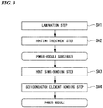
- the ceramic substrate 11, the filler metals 25, the active metal materials 26, and the copper sheets 22 and 23 are loaded and heated in a vacuum-heating furnace in a state of being pressurized in the lamination direction at 1 kgf/cm 2 to 35 kgf/cm 2 (98 kPa to 3430 kPa) (heating treatment step S02).
- the pressure in the vacuum-heating furnace is set in a range of 10 -6 Pa to 10 -3 Pa
- the heating temperature is set in a range of 560°C to 650°C
- the heating time is set in a range of 30 minutes to 360 minutes.
- the melting point of the filler metal 25 is set to 710°C or lower, it is possible to make the filler metal form a liquid phase at a lower temperature than in a case in which the Ag-Cu-Ti-based brazing filler metal is used.
- the ceramic substrate 11 and the copper sheets 22 and 23 are bonded together using the filler metals 25 which do not contain Ag, it is possible to reduce the manufacturing cost more than in a case in which the Ag-Cu-Ti-based brazing filler metal is used.
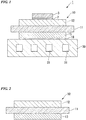
- the power-module substrate 110 includes the ceramic substrate 11, the circuit layer 112 disposed on one surface (the upper surface in Fig. 5 ) of the ceramic substrate 11, and a metal layer 113 disposed on the other side (the lower surface in Fig. 5 ) of the ceramic substrate 11.
- the circuit layer 112 is formed by bonding a conductive metal sheet of copper or a copper alloy to one surface of the ceramic substrate 11.
- the circuit layer 112 is formed by bonding a rolled sheet of copper having a purity of 99.99% by mass or greater.
- the thickness of the circuit layer 112 is set in a range of 0.1 mm to 1.0 mm and, in the present embodiment, is set to 0.4 mm.
- the semiconductor element 3 is bonded to the upper surface of the circuit layer 112 in the power-module substrate 110 through a solder material (semiconductor element-bonding step S15).
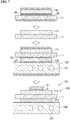
- the brazing filler metals are disposed on the copper member sides, and the heating treatment is carried out, it is also possible to bond the ceramic member and the copper member.
- a filler metal 225 is disposed between the active metal material 226 and a copper member 222, and a heating treatment is carried out in a state in which the active metal material and the filler metal are laminated and pressured in the lamination direction, the active metal material 226 and the copper member 222 can be bonded together.
- an aluminum sheet having a purity of 99.99% was laminated on the other surface of the ceramic substrate through an Al-Si-based brazing filler metal, the components were loaded and heated in a vacuum-heating furnace at 640°C for 30 minutes in a state of being pressurized in the lamination direction at a pressure of 5 kgf/cm 2 (490 kPa), whereby an aluminum sheet was bonded to the other surface of the ceramic substrate, and a power-module substrate of Invention Example 11 was obtained.
- the initial bonding area referred to an area to be bonded before bonding, that is, the area of the circuit layer in the present embodiment.
- the ultrasonic flaw detector exfoliation was observed at white portions in the bonding portion, and thus the area of these white portions was considered as the exfoliation area.
- Bonding rate % Initial bonding area ⁇ Exfoliation area Initial bonding area ⁇ 100
- the present invention relates to a method for manufacturing a power-module substrate in which a ceramic member and a copper member can be bonded together at a low temperature and, furthermore, the manufacturing cost is low.
Claims (12)
- Procédé de fabrication d'un corps collé formé par collage d'un organe en céramique constitué d'un organe en céramique et d'un organe en cuivre constitué de cuivre ou d'un alliage de cuivre, le procédé comprenant :une étape de stratification consistant à stratifier l'organe en céramique et l'organe en cuivre par l'intermédiaire d'un matériau de métal actif et d'un métal de charge ayant un point de fusion de 710 °C ou moins ; etune étape de traitement thermique consistant à chauffer l'organe en céramique et l'organe en cuivre stratifiés ensemble pour coller l'organe en céramique et l'organe en cuivre dans un état où ils sont soumis dans la direction de stratification à une pression de 0,098 MPa à 3,43 MPa (1 kgf/cm2 à 35 kgf/cm2),dans lequel le métal de charge est un métal de charge de brasage ayant une température du liquidus de 450 °C ou plus ou un matériau de soudure ayant une température du liquidus inférieure à 450 °C,le métal de charge de brasage est l'un quelconque choisi dans le groupe d'un métal de charge de brasage à base de Cu-P, d'un métal de charge de brasage à base de Cu-Sn et d'un métal de charge de brasage à base de Cu-Al, etle matériau de soudure est un matériau de soudure à base de Cu-P-Sn-Ni ou un matériau de soudure à base de Cu-Sn.
- Procédé de fabrication d'un corps collé selon la revendication 1,
dans lequel le métal de charge est disposé sur l'organe en céramique, et le matériau de métal actif est disposé sur l'organe en cuivre dans l'étape de stratification. - Procédé de fabrication d'un corps collé selon la revendication 1 ou 2,
dans lequel le métal de charge est le métal de charge de brasage. - Procédé de fabrication d'un corps collé selon la revendication 1,
dans lequel le métal de charge de brasage est le métal de charge de brasage à base de Cu-P ou le métal de charge de brasage à base de Cu-Al. - Procédé de fabrication d'un corps collé selon la revendication 1 ou 2,
dans lequel le métal de charge est le matériau de soudure. - Procédé de fabrication d'un corps collé selon la revendication 1,
dans lequel le matériau de soudure est le matériau de soudure à base de Cu-P-Sn-Ni. - Procédé de fabrication d'un corps collé selon l'une quelconque des revendications 1 à 6,
dans lequel le matériau de métal actif est un matériau de Ti. - Procédé de fabrication d'un substrat de module de puissance ayant un substrat en céramique et une couche de circuit constituée de cuivre ou d'un alliage de cuivre, la couche de circuit étant disposée sur une première surface du substrat en céramique, le procédé comprenant
le collage de la couche de circuit sur la première surface du substrat en céramique au moyen du procédé de fabrication d'un corps collé selon l'une quelconque des revendications 1 à 7. - Procédé de fabrication d'un substrat de module de puissance ayant un substrat en céramique, une couche de circuit constituée de cuivre ou d'un alliage de cuivre, et une couche de métal constituée de cuivre ou d'un alliage de cuivre, la couche de circuit étant disposée sur une première surface du substrat en céramique, et la couche de métal étant disposée sur l'autre surface du substrat en céramique, le procédé comprenant :le collage de la couche de circuit et de la couche de métal respectivement sur les deux surfaces du substrat en céramique au moyen du procédé de fabrication d'un corps collé selon l'une quelconque des revendications 1 à 7.
- Procédé de fabrication d'un substrat de module de puissance ayant un substrat en céramique, une couche de circuit constituée de cuivre ou d'un alliage de cuivre, et une couche de métal constituée d'aluminium ou d'un alliage d'aluminium, la couche de circuit étant disposée sur une première surface du substrat en céramique, et la couche de métal étant disposée sur l'autre surface du substrat en céramique, le procédé comprenant :le collage de la couche de circuit sur la première surface du substrat en céramique au moyen du procédé de fabrication d'un corps collé selon l'une quelconque des revendications 1 à 7, etle collage de la couche de métal sur l'autre surface du substrat en céramique après collage du substrat en céramique et de la couche de circuit.
- Procédé de fabrication d'un corps collé selon la revendication 2,
dans lequel une épaisseur du métal de charge est de 5 µm à 150 µm. - Procédé de fabrication d'un corps collé selon la revendication 2,
dans lequel une épaisseur du matériau de métal actif est de 1 µm à 20 µm.
Applications Claiming Priority (2)
| Application Number | Priority Date | Filing Date | Title |
|---|---|---|---|
| JP2013055517A JP5672324B2 (ja) | 2013-03-18 | 2013-03-18 | 接合体の製造方法及びパワーモジュール用基板の製造方法 |
| PCT/JP2014/057121 WO2014148425A1 (fr) | 2013-03-18 | 2014-03-17 | Procédé de fabrication de corps collé et procédé de fabrication de substrat de module de puissance |
Publications (3)
| Publication Number | Publication Date |
|---|---|
| EP2978019A1 EP2978019A1 (fr) | 2016-01-27 |
| EP2978019A4 EP2978019A4 (fr) | 2016-11-02 |
| EP2978019B1 true EP2978019B1 (fr) | 2018-01-31 |
Family
ID=51580104
Family Applications (1)
| Application Number | Title | Priority Date | Filing Date |
|---|---|---|---|
| EP14769861.7A Active EP2978019B1 (fr) | 2013-03-18 | 2014-03-17 | Procédé de fabrication de corps assemblé et procédé de fabrication de substrat de module de puissance |
Country Status (7)
| Country | Link |
|---|---|
| US (1) | US10199237B2 (fr) |
| EP (1) | EP2978019B1 (fr) |
| JP (1) | JP5672324B2 (fr) |
| KR (1) | KR102220852B1 (fr) |
| CN (1) | CN105190869B (fr) |
| TW (1) | TWI609461B (fr) |
| WO (1) | WO2014148425A1 (fr) |
Families Citing this family (16)
| Publication number | Priority date | Publication date | Assignee | Title |
|---|---|---|---|---|
| JP5672324B2 (ja) | 2013-03-18 | 2015-02-18 | 三菱マテリアル株式会社 | 接合体の製造方法及びパワーモジュール用基板の製造方法 |
| JP6111764B2 (ja) * | 2013-03-18 | 2017-04-12 | 三菱マテリアル株式会社 | パワーモジュール用基板の製造方法 |
| WO2015029811A1 (fr) * | 2013-08-26 | 2015-03-05 | 三菱マテリアル株式会社 | Assemblage et substrat de module d'alimentation |
| JP5720839B2 (ja) | 2013-08-26 | 2015-05-20 | 三菱マテリアル株式会社 | 接合体及びパワーモジュール用基板 |
| JP6127833B2 (ja) * | 2013-08-26 | 2017-05-17 | 三菱マテリアル株式会社 | 接合体の製造方法及びパワーモジュール用基板の製造方法 |
| JP6079505B2 (ja) | 2013-08-26 | 2017-02-15 | 三菱マテリアル株式会社 | 接合体及びパワーモジュール用基板 |
| JP6256176B2 (ja) | 2014-04-25 | 2018-01-10 | 三菱マテリアル株式会社 | 接合体の製造方法、パワーモジュール用基板の製造方法 |
| JP6819299B2 (ja) | 2016-01-22 | 2021-01-27 | 三菱マテリアル株式会社 | 接合体、パワーモジュール用基板、接合体の製造方法及びパワーモジュール用基板の製造方法 |
| WO2017126641A1 (fr) * | 2016-01-22 | 2017-07-27 | 三菱マテリアル株式会社 | Corps lié ainsi que procédé de fabrication de celui-ci, et substrat pour module de puissance ainsi que procédé de fabrication de celui-ci |
| JP6652856B2 (ja) * | 2016-02-25 | 2020-02-26 | 株式会社フジクラ | 半導体レーザモジュール及びその製造方法 |
| JP7124633B2 (ja) * | 2017-10-27 | 2022-08-24 | 三菱マテリアル株式会社 | 接合体、及び、絶縁回路基板 |
| KR102483328B1 (ko) | 2017-11-13 | 2022-12-30 | 삼성전자주식회사 | 복수개의 전자 장치들 간의 거리 측정 방법 및 그에 따른 전자 장치 |
| WO2019180913A1 (fr) * | 2018-03-23 | 2019-09-26 | 三菱マテリアル株式会社 | Procédé de fabrication de module monté sur composant électronique |
| EP3780087A4 (fr) * | 2018-03-26 | 2022-01-12 | Mitsubishi Materials Corporation | Procédé de fabrication d'un corps lié pour carte de circuit imprimé isolante, et corps lié pour carte de circuit imprimé isolante |
| WO2020044594A1 (fr) * | 2018-08-28 | 2020-03-05 | 三菱マテリアル株式会社 | Corps assemblé en cuivre/céramique, carte de circuit imprimé isolée, procédé de production de corps assemblé en cuivre/céramique, et procédé de fabrication de carte de circuit imprimé isolée |
| DE102019135171A1 (de) * | 2019-12-19 | 2021-06-24 | Rogers Germany Gmbh | Lotmaterial, Verfahren zur Herstellung eines solchen Lotmaterials und Verwendung eines solchen Lotmaterials zur Anbindung einer Metallschicht an eine Keramikschicht |
Family Cites Families (56)
| Publication number | Priority date | Publication date | Assignee | Title |
|---|---|---|---|---|
| US153618A (en) * | 1874-07-28 | Improvement in lock-hinges | ||
| JPH0810710B2 (ja) * | 1984-02-24 | 1996-01-31 | 株式会社東芝 | 良熱伝導性基板の製造方法 |
| JPS63239166A (ja) | 1987-03-27 | 1988-10-05 | 株式会社東芝 | セラミツクス接合体 |
| US5378294A (en) | 1989-11-17 | 1995-01-03 | Outokumpu Oy | Copper alloys to be used as brazing filler metals |
| JPH03297595A (ja) * | 1990-04-18 | 1991-12-27 | Meidensha Corp | ロウ材とロウ付け方法 |
| WO2004074210A1 (fr) | 1992-07-03 | 2004-09-02 | Masanori Hirano | Corps composite a base de ceramique et de metal et son procede de production |
| JPH07308794A (ja) * | 1994-05-19 | 1995-11-28 | Showa Alum Corp | 低温ろう付用ろう材 |
| JP3211856B2 (ja) | 1994-11-02 | 2001-09-25 | 電気化学工業株式会社 | 回路基板 |
| JP4077888B2 (ja) * | 1995-07-21 | 2008-04-23 | 株式会社東芝 | セラミックス回路基板 |
| JPH10102167A (ja) * | 1996-09-25 | 1998-04-21 | Toyota Central Res & Dev Lab Inc | 銅系低融点ろう材 |
| US6261703B1 (en) * | 1997-05-26 | 2001-07-17 | Sumitomo Electric Industries, Ltd. | Copper circuit junction substrate and method of producing the same |
| JP2000119071A (ja) | 1998-10-14 | 2000-04-25 | Fuji Electric Co Ltd | 半導体装置用セラミックス基板 |
| JP2001148451A (ja) | 1999-03-24 | 2001-05-29 | Mitsubishi Materials Corp | パワーモジュール用基板 |
| JP2000349400A (ja) | 1999-06-04 | 2000-12-15 | Denki Kagaku Kogyo Kk | 回路基板 |
| CN1240515C (zh) | 2001-02-27 | 2006-02-08 | 日商·胜美达股份有限公司 | 无铅焊锡合金及使用该合金的电子部件 |
| JP2003197826A (ja) * | 2001-12-26 | 2003-07-11 | Toshiba Corp | セラミックス回路基板およびそれを用いた半導体モジュール |
| US9533379B2 (en) * | 2002-08-23 | 2017-01-03 | Lincoln Global, Inc. | Phosphorous-copper base brazing alloy |
| JP4206915B2 (ja) | 2002-12-27 | 2009-01-14 | 三菱マテリアル株式会社 | パワーモジュール用基板 |
| JP4394477B2 (ja) * | 2003-03-27 | 2010-01-06 | Dowaホールディングス株式会社 | 金属−セラミックス接合基板の製造方法 |
| CA2525386A1 (fr) | 2003-05-13 | 2005-01-20 | Reactive Nanotechnologies, Inc. | Procede de commande d'ondes thermiques dans une liaison multicouche reactive et produit ainsi obtenu |
| JP4362597B2 (ja) | 2003-05-30 | 2009-11-11 | Dowaメタルテック株式会社 | 金属−セラミックス回路基板およびその製造方法 |
| JP2005050919A (ja) * | 2003-07-30 | 2005-02-24 | Ngk Spark Plug Co Ltd | 回路基板および半導体装置 |
| JP2005052869A (ja) | 2003-08-06 | 2005-03-03 | Sumitomo Metal Mining Co Ltd | 高温はんだ付用ろう材とそれを用いた半導体装置 |
| JP4115979B2 (ja) | 2004-09-24 | 2008-07-09 | 株式会社東芝 | 非鉛系はんだ材 |
| JP4207896B2 (ja) | 2005-01-19 | 2009-01-14 | 富士電機デバイステクノロジー株式会社 | 半導体装置 |
| EP1858078A4 (fr) | 2005-01-20 | 2009-03-04 | Almt Corp | Element pour un dispositif semi-conducteur et procede pour sa fabrication |
| DE102005032076B3 (de) | 2005-07-08 | 2007-02-08 | Infineon Technologies Ag | Verfahren zum Herstellen eines Schaltungsmoduls |
| DE102005061049A1 (de) | 2005-12-19 | 2007-06-21 | Curamik Electronics Gmbh | Metall-Keramik-Substrat |
| US8164176B2 (en) | 2006-10-20 | 2012-04-24 | Infineon Technologies Ag | Semiconductor module arrangement |
| JP2008198706A (ja) | 2007-02-09 | 2008-08-28 | Hitachi Metals Ltd | 回路基板、その製造方法およびそれを用いた半導体モジュール |
| JP4964009B2 (ja) * | 2007-04-17 | 2012-06-27 | 株式会社豊田中央研究所 | パワー半導体モジュール |
| DE102008001226A1 (de) | 2007-04-24 | 2008-10-30 | Ceramtec Ag | Bauteil mit einem metallisierten Keramikkörper |
| US7821130B2 (en) | 2008-03-31 | 2010-10-26 | Infineon Technologies Ag | Module including a rough solder joint |
| WO2009148168A1 (fr) | 2008-06-06 | 2009-12-10 | 三菱マテリアル株式会社 | Module de puissance, son substrat, et procédé de production de ce substrat |
| US20100175756A1 (en) | 2009-01-15 | 2010-07-15 | Weihs Timothy P | Method For Bonding Of Concentrating Photovoltaic Receiver Module To Heat Sink Using Foil And Solder |
| WO2010088504A1 (fr) | 2009-01-29 | 2010-08-05 | Smith International, Inc. | Procédés de brasage pour des dispositifs de coupe pdc |
| JP5504842B2 (ja) | 2009-11-20 | 2014-05-28 | 三菱マテリアル株式会社 | パワーモジュール用基板、ヒートシンク付パワーモジュール用基板、パワーモジュール及びパワーモジュール用基板の製造方法 |
| JP5363361B2 (ja) * | 2010-01-28 | 2013-12-11 | 本田技研工業株式会社 | 半導体装置及びその製造方法 |
| JP5577980B2 (ja) | 2010-09-16 | 2014-08-27 | 三菱マテリアル株式会社 | ヒートシンク付パワーモジュール用基板、パワーモジュール及びヒートシンク付パワーモジュール用基板の製造方法 |
| JP2012136378A (ja) | 2010-12-25 | 2012-07-19 | Kyocera Corp | 回路基板およびこれを用いた電子装置 |
| JP5736807B2 (ja) | 2011-02-02 | 2015-06-17 | 三菱マテリアル株式会社 | ヒートシンク付パワーモジュール用基板、ヒートシンク付パワーモジュール用基板の製造方法及びパワーモジュール |
| JP2012178513A (ja) | 2011-02-28 | 2012-09-13 | Mitsubishi Materials Corp | パワーモジュールユニット及びパワーモジュールユニットの製造方法 |
| CN103687829A (zh) | 2011-07-20 | 2014-03-26 | 戴蒙得创新股份有限公司 | 钎焊的涂布的含金刚石材料 |
| WO2013018504A1 (fr) | 2011-08-04 | 2013-02-07 | 三菱電機株式会社 | Dispositif à semi-conducteur et son procédé de production |
| JP5218621B2 (ja) * | 2011-10-28 | 2013-06-26 | 日立金属株式会社 | 回路基板およびこれを用いた半導体モジュール |
| EP2811513B1 (fr) | 2012-02-01 | 2019-12-18 | Mitsubishi Materials Corporation | Procédé de fabrication de substrat pour modules de courant |
| JP2013229579A (ja) | 2012-03-30 | 2013-11-07 | Mitsubishi Materials Corp | パワーモジュール用基板、ヒートシンク付パワーモジュール用基板及びパワーモジュール |
| JP6044097B2 (ja) | 2012-03-30 | 2016-12-14 | 三菱マテリアル株式会社 | ヒートシンク付パワーモジュール用基板、冷却器付パワーモジュール用基板及びパワーモジュール |
| JP5614485B2 (ja) | 2012-10-16 | 2014-10-29 | 三菱マテリアル株式会社 | ヒートシンク付パワーモジュール用基板、ヒートシンク付パワーモジュール、及びヒートシンク付パワーモジュール用基板の製造方法 |
| CN102922828B (zh) | 2012-10-24 | 2015-04-22 | 浙江工贸职业技术学院 | 铜箔键合陶瓷基板的复合板及其制备方法 |
| JP6056432B2 (ja) | 2012-12-06 | 2017-01-11 | 三菱マテリアル株式会社 | パワーモジュール用基板、ヒートシンク付パワーモジュール用基板、パワーモジュール、パワーモジュール用基板の製造方法 |
| JP5664679B2 (ja) | 2013-03-07 | 2015-02-04 | 三菱マテリアル株式会社 | パワーモジュール用基板の製造方法 |
| EP2974859B1 (fr) | 2013-03-14 | 2020-10-14 | Mitsubishi Materials Corporation | Corps collé, substrat pour modules électriques, et substrat avec dissipateur de chaleur pour modules électriques |
| JP6111764B2 (ja) * | 2013-03-18 | 2017-04-12 | 三菱マテリアル株式会社 | パワーモジュール用基板の製造方法 |
| JP5672324B2 (ja) | 2013-03-18 | 2015-02-18 | 三菱マテリアル株式会社 | 接合体の製造方法及びパワーモジュール用基板の製造方法 |
| JP3211856U (ja) | 2017-05-09 | 2017-08-10 | 株式会社アイエスピー | メジャー付きタオル |
-
2013
- 2013-03-18 JP JP2013055517A patent/JP5672324B2/ja active Active
-
2014
- 2014-03-17 KR KR1020157025321A patent/KR102220852B1/ko active IP Right Grant
- 2014-03-17 WO PCT/JP2014/057121 patent/WO2014148425A1/fr active Application Filing
- 2014-03-17 EP EP14769861.7A patent/EP2978019B1/fr active Active
- 2014-03-17 CN CN201480012947.2A patent/CN105190869B/zh active Active
- 2014-03-17 US US14/775,819 patent/US10199237B2/en active Active
- 2014-03-18 TW TW103110092A patent/TWI609461B/zh active
Non-Patent Citations (1)
| Title |
|---|
| None * |
Also Published As
| Publication number | Publication date |
|---|---|
| US10199237B2 (en) | 2019-02-05 |
| KR20150133194A (ko) | 2015-11-27 |
| JP2014183118A (ja) | 2014-09-29 |
| KR102220852B1 (ko) | 2021-02-25 |
| CN105190869A (zh) | 2015-12-23 |
| EP2978019A4 (fr) | 2016-11-02 |
| JP5672324B2 (ja) | 2015-02-18 |
| US20160013073A1 (en) | 2016-01-14 |
| CN105190869B (zh) | 2018-08-10 |
| EP2978019A1 (fr) | 2016-01-27 |
| TWI609461B (zh) | 2017-12-21 |
| TW201508870A (zh) | 2015-03-01 |
| WO2014148425A1 (fr) | 2014-09-25 |
Similar Documents
| Publication | Publication Date | Title |
|---|---|---|
| EP2978019B1 (fr) | Procédé de fabrication de corps assemblé et procédé de fabrication de substrat de module de puissance | |
| EP2978018B1 (fr) | Procédé de fabrication d'un substrat de module de puissance | |
| EP2950340B1 (fr) | Substrat de module d'alimentation, substrat de module d'alimentation à dissipateur de chaleur, et module d'alimentation à dissipateur de chaleur | |
| KR102219145B1 (ko) | 접합체 및 파워 모듈용 기판 | |
| EP2980844B1 (fr) | Substrat pour des modules de puissance, substrat ayant un dissipateur thermique pour des modules de puissance, et module de puissance | |
| EP2833399B1 (fr) | Substrat de module de puissance, substrat de module de puissance muni de dissipateur thermique, et module de puissance | |
| KR102422607B1 (ko) | 접합체, 히트 싱크가 부착된 파워 모듈용 기판, 히트 싱크, 및 접합체의 제조 방법, 히트 싱크가 부착된 파워 모듈용 기판의 제조 방법, 히트 싱크의 제조 방법 | |
| KR102027615B1 (ko) | 히트 싱크 장착 파워 모듈용 기판, 냉각기 장착 파워 모듈용 기판 및 파워 모듈 | |
| KR102154882B1 (ko) | 파워 모듈 | |
| EP3041042A1 (fr) | Procédé de fabrication d'un ensemble et procédé de fabrication de substrat de module de puissance | |
| EP3041044B1 (fr) | Corps collé et substrat de module de puissance | |
| WO2003046981A1 (fr) | Structure de module et module comprenant celle-ci | |
| EP3605601B1 (fr) | Procédé de production d'une carte de circuit imprimé isolée pourvue d'un dissipateur thermique | |
| EP3162781B1 (fr) | Procédé de production de corps collé en céramique-aluminium, procédé de production de substrat de module de puissance, corps collé en céramique-aluminium et substrat de module de puissance | |
| JP2008147309A (ja) | セラミックス基板およびこれを用いた半導体モジュール | |
| KR20180104659A (ko) | 접합체, 파워 모듈용 기판, 접합체의 제조 방법 및 파워 모듈용 기판의 제조 방법 | |
| CN109075135B (zh) | 接合体、功率模块用基板、接合体的制造方法及功率模块用基板的制造方法 | |
| JP2001267468A (ja) | セラミックス回路基板複合体 |
Legal Events
| Date | Code | Title | Description |
|---|---|---|---|
| PUAI | Public reference made under article 153(3) epc to a published international application that has entered the european phase |
Free format text: ORIGINAL CODE: 0009012 |
|
| 17P | Request for examination filed |
Effective date: 20150910 |
|
| AK | Designated contracting states |
Kind code of ref document: A1 Designated state(s): AL AT BE BG CH CY CZ DE DK EE ES FI FR GB GR HR HU IE IS IT LI LT LU LV MC MK MT NL NO PL PT RO RS SE SI SK SM TR |
|
| AX | Request for extension of the european patent |
Extension state: BA ME |
|
| DAX | Request for extension of the european patent (deleted) | ||
| A4 | Supplementary search report drawn up and despatched |
Effective date: 20161006 |
|
| RIC1 | Information provided on ipc code assigned before grant |
Ipc: H01L 23/12 20060101AFI20160929BHEP Ipc: H01L 23/14 20060101ALI20160929BHEP Ipc: C04B 37/02 20060101ALI20160929BHEP |
|
| GRAP | Despatch of communication of intention to grant a patent |
Free format text: ORIGINAL CODE: EPIDOSNIGR1 |
|
| INTG | Intention to grant announced |
Effective date: 20170905 |
|
| GRAS | Grant fee paid |
Free format text: ORIGINAL CODE: EPIDOSNIGR3 |
|
| GRAA | (expected) grant |
Free format text: ORIGINAL CODE: 0009210 |
|
| AK | Designated contracting states |
Kind code of ref document: B1 Designated state(s): AL AT BE BG CH CY CZ DE DK EE ES FI FR GB GR HR HU IE IS IT LI LT LU LV MC MK MT NL NO PL PT RO RS SE SI SK SM TR |
|
| REG | Reference to a national code |
Ref country code: GB Ref legal event code: FG4D Ref country code: CH Ref legal event code: EP |
|
| REG | Reference to a national code |
Ref country code: AT Ref legal event code: REF Ref document number: 968081 Country of ref document: AT Kind code of ref document: T Effective date: 20180215 |
|
| REG | Reference to a national code |
Ref country code: IE Ref legal event code: FG4D |
|
| REG | Reference to a national code |
Ref country code: DE Ref legal event code: R096 Ref document number: 602014020470 Country of ref document: DE |
|
| REG | Reference to a national code |
Ref country code: NL Ref legal event code: MP Effective date: 20180131 |
|
| REG | Reference to a national code |
Ref country code: LT Ref legal event code: MG4D |
|
| REG | Reference to a national code |
Ref country code: AT Ref legal event code: MK05 Ref document number: 968081 Country of ref document: AT Kind code of ref document: T Effective date: 20180131 |
|
| PG25 | Lapsed in a contracting state [announced via postgrant information from national office to epo] |
Ref country code: NL Free format text: LAPSE BECAUSE OF FAILURE TO SUBMIT A TRANSLATION OF THE DESCRIPTION OR TO PAY THE FEE WITHIN THE PRESCRIBED TIME-LIMIT Effective date: 20180131 Ref country code: ES Free format text: LAPSE BECAUSE OF FAILURE TO SUBMIT A TRANSLATION OF THE DESCRIPTION OR TO PAY THE FEE WITHIN THE PRESCRIBED TIME-LIMIT Effective date: 20180131 Ref country code: LT Free format text: LAPSE BECAUSE OF FAILURE TO SUBMIT A TRANSLATION OF THE DESCRIPTION OR TO PAY THE FEE WITHIN THE PRESCRIBED TIME-LIMIT Effective date: 20180131 Ref country code: HR Free format text: LAPSE BECAUSE OF FAILURE TO SUBMIT A TRANSLATION OF THE DESCRIPTION OR TO PAY THE FEE WITHIN THE PRESCRIBED TIME-LIMIT Effective date: 20180131 Ref country code: FI Free format text: LAPSE BECAUSE OF FAILURE TO SUBMIT A TRANSLATION OF THE DESCRIPTION OR TO PAY THE FEE WITHIN THE PRESCRIBED TIME-LIMIT Effective date: 20180131 Ref country code: NO Free format text: LAPSE BECAUSE OF FAILURE TO SUBMIT A TRANSLATION OF THE DESCRIPTION OR TO PAY THE FEE WITHIN THE PRESCRIBED TIME-LIMIT Effective date: 20180430 |
|
| PG25 | Lapsed in a contracting state [announced via postgrant information from national office to epo] |
Ref country code: RS Free format text: LAPSE BECAUSE OF FAILURE TO SUBMIT A TRANSLATION OF THE DESCRIPTION OR TO PAY THE FEE WITHIN THE PRESCRIBED TIME-LIMIT Effective date: 20180131 Ref country code: PL Free format text: LAPSE BECAUSE OF FAILURE TO SUBMIT A TRANSLATION OF THE DESCRIPTION OR TO PAY THE FEE WITHIN THE PRESCRIBED TIME-LIMIT Effective date: 20180131 Ref country code: LV Free format text: LAPSE BECAUSE OF FAILURE TO SUBMIT A TRANSLATION OF THE DESCRIPTION OR TO PAY THE FEE WITHIN THE PRESCRIBED TIME-LIMIT Effective date: 20180131 Ref country code: SE Free format text: LAPSE BECAUSE OF FAILURE TO SUBMIT A TRANSLATION OF THE DESCRIPTION OR TO PAY THE FEE WITHIN THE PRESCRIBED TIME-LIMIT Effective date: 20180131 Ref country code: IS Free format text: LAPSE BECAUSE OF FAILURE TO SUBMIT A TRANSLATION OF THE DESCRIPTION OR TO PAY THE FEE WITHIN THE PRESCRIBED TIME-LIMIT Effective date: 20180531 Ref country code: BG Free format text: LAPSE BECAUSE OF FAILURE TO SUBMIT A TRANSLATION OF THE DESCRIPTION OR TO PAY THE FEE WITHIN THE PRESCRIBED TIME-LIMIT Effective date: 20180430 Ref country code: GR Free format text: LAPSE BECAUSE OF FAILURE TO SUBMIT A TRANSLATION OF THE DESCRIPTION OR TO PAY THE FEE WITHIN THE PRESCRIBED TIME-LIMIT Effective date: 20180501 Ref country code: AT Free format text: LAPSE BECAUSE OF FAILURE TO SUBMIT A TRANSLATION OF THE DESCRIPTION OR TO PAY THE FEE WITHIN THE PRESCRIBED TIME-LIMIT Effective date: 20180131 |
|
| PG25 | Lapsed in a contracting state [announced via postgrant information from national office to epo] |
Ref country code: AL Free format text: LAPSE BECAUSE OF FAILURE TO SUBMIT A TRANSLATION OF THE DESCRIPTION OR TO PAY THE FEE WITHIN THE PRESCRIBED TIME-LIMIT Effective date: 20180131 Ref country code: IT Free format text: LAPSE BECAUSE OF FAILURE TO SUBMIT A TRANSLATION OF THE DESCRIPTION OR TO PAY THE FEE WITHIN THE PRESCRIBED TIME-LIMIT Effective date: 20180131 Ref country code: EE Free format text: LAPSE BECAUSE OF FAILURE TO SUBMIT A TRANSLATION OF THE DESCRIPTION OR TO PAY THE FEE WITHIN THE PRESCRIBED TIME-LIMIT Effective date: 20180131 Ref country code: RO Free format text: LAPSE BECAUSE OF FAILURE TO SUBMIT A TRANSLATION OF THE DESCRIPTION OR TO PAY THE FEE WITHIN THE PRESCRIBED TIME-LIMIT Effective date: 20180131 |
|
| REG | Reference to a national code |
Ref country code: CH Ref legal event code: PL |
|
| REG | Reference to a national code |
Ref country code: DE Ref legal event code: R097 Ref document number: 602014020470 Country of ref document: DE |
|
| PG25 | Lapsed in a contracting state [announced via postgrant information from national office to epo] |
Ref country code: SM Free format text: LAPSE BECAUSE OF FAILURE TO SUBMIT A TRANSLATION OF THE DESCRIPTION OR TO PAY THE FEE WITHIN THE PRESCRIBED TIME-LIMIT Effective date: 20180131 Ref country code: SK Free format text: LAPSE BECAUSE OF FAILURE TO SUBMIT A TRANSLATION OF THE DESCRIPTION OR TO PAY THE FEE WITHIN THE PRESCRIBED TIME-LIMIT Effective date: 20180131 Ref country code: MC Free format text: LAPSE BECAUSE OF FAILURE TO SUBMIT A TRANSLATION OF THE DESCRIPTION OR TO PAY THE FEE WITHIN THE PRESCRIBED TIME-LIMIT Effective date: 20180131 Ref country code: CZ Free format text: LAPSE BECAUSE OF FAILURE TO SUBMIT A TRANSLATION OF THE DESCRIPTION OR TO PAY THE FEE WITHIN THE PRESCRIBED TIME-LIMIT Effective date: 20180131 Ref country code: DK Free format text: LAPSE BECAUSE OF FAILURE TO SUBMIT A TRANSLATION OF THE DESCRIPTION OR TO PAY THE FEE WITHIN THE PRESCRIBED TIME-LIMIT Effective date: 20180131 |
|
| PLBE | No opposition filed within time limit |
Free format text: ORIGINAL CODE: 0009261 |
|
| STAA | Information on the status of an ep patent application or granted ep patent |
Free format text: STATUS: NO OPPOSITION FILED WITHIN TIME LIMIT |
|
| REG | Reference to a national code |
Ref country code: BE Ref legal event code: MM Effective date: 20180331 |
|
| GBPC | Gb: european patent ceased through non-payment of renewal fee |
Effective date: 20180430 |
|
| REG | Reference to a national code |
Ref country code: IE Ref legal event code: MM4A |
|
| PG25 | Lapsed in a contracting state [announced via postgrant information from national office to epo] |
Ref country code: LU Free format text: LAPSE BECAUSE OF NON-PAYMENT OF DUE FEES Effective date: 20180317 |
|
| 26N | No opposition filed |
Effective date: 20181102 |
|
| PG25 | Lapsed in a contracting state [announced via postgrant information from national office to epo] |
Ref country code: IE Free format text: LAPSE BECAUSE OF NON-PAYMENT OF DUE FEES Effective date: 20180317 |
|
| PG25 | Lapsed in a contracting state [announced via postgrant information from national office to epo] |
Ref country code: GB Free format text: LAPSE BECAUSE OF NON-PAYMENT OF DUE FEES Effective date: 20180430 Ref country code: LI Free format text: LAPSE BECAUSE OF NON-PAYMENT OF DUE FEES Effective date: 20180331 Ref country code: CH Free format text: LAPSE BECAUSE OF NON-PAYMENT OF DUE FEES Effective date: 20180331 Ref country code: SI Free format text: LAPSE BECAUSE OF FAILURE TO SUBMIT A TRANSLATION OF THE DESCRIPTION OR TO PAY THE FEE WITHIN THE PRESCRIBED TIME-LIMIT Effective date: 20180131 Ref country code: BE Free format text: LAPSE BECAUSE OF NON-PAYMENT OF DUE FEES Effective date: 20180331 |
|
| PG25 | Lapsed in a contracting state [announced via postgrant information from national office to epo] |
Ref country code: FR Free format text: LAPSE BECAUSE OF NON-PAYMENT OF DUE FEES Effective date: 20180331 |
|
| PG25 | Lapsed in a contracting state [announced via postgrant information from national office to epo] |
Ref country code: MT Free format text: LAPSE BECAUSE OF NON-PAYMENT OF DUE FEES Effective date: 20180317 |
|
| PG25 | Lapsed in a contracting state [announced via postgrant information from national office to epo] |
Ref country code: TR Free format text: LAPSE BECAUSE OF FAILURE TO SUBMIT A TRANSLATION OF THE DESCRIPTION OR TO PAY THE FEE WITHIN THE PRESCRIBED TIME-LIMIT Effective date: 20180131 |
|
| PG25 | Lapsed in a contracting state [announced via postgrant information from national office to epo] |
Ref country code: PT Free format text: LAPSE BECAUSE OF FAILURE TO SUBMIT A TRANSLATION OF THE DESCRIPTION OR TO PAY THE FEE WITHIN THE PRESCRIBED TIME-LIMIT Effective date: 20180131 |
|
| PG25 | Lapsed in a contracting state [announced via postgrant information from national office to epo] |
Ref country code: CY Free format text: LAPSE BECAUSE OF FAILURE TO SUBMIT A TRANSLATION OF THE DESCRIPTION OR TO PAY THE FEE WITHIN THE PRESCRIBED TIME-LIMIT Effective date: 20180131 Ref country code: MK Free format text: LAPSE BECAUSE OF NON-PAYMENT OF DUE FEES Effective date: 20180131 Ref country code: HU Free format text: LAPSE BECAUSE OF FAILURE TO SUBMIT A TRANSLATION OF THE DESCRIPTION OR TO PAY THE FEE WITHIN THE PRESCRIBED TIME-LIMIT; INVALID AB INITIO Effective date: 20140317 |
|
| PGFP | Annual fee paid to national office [announced via postgrant information from national office to epo] |
Ref country code: DE Payment date: 20230321 Year of fee payment: 10 |