EP2977792A1 - A ct detector - Google Patents
A ct detector Download PDFInfo
- Publication number
- EP2977792A1 EP2977792A1 EP15177549.1A EP15177549A EP2977792A1 EP 2977792 A1 EP2977792 A1 EP 2977792A1 EP 15177549 A EP15177549 A EP 15177549A EP 2977792 A1 EP2977792 A1 EP 2977792A1
- Authority
- EP
- European Patent Office
- Prior art keywords
- detector
- grids
- gaps
- rays
- present
- Prior art date
- Legal status (The legal status is an assumption and is not a legal conclusion. Google has not performed a legal analysis and makes no representation as to the accuracy of the status listed.)
- Granted
Links
Images


Classifications
-
- G—PHYSICS
- G01—MEASURING; TESTING
- G01T—MEASUREMENT OF NUCLEAR OR X-RADIATION
- G01T1/00—Measuring X-radiation, gamma radiation, corpuscular radiation, or cosmic radiation
- G01T1/16—Measuring radiation intensity
- G01T1/20—Measuring radiation intensity with scintillation detectors
- G01T1/2002—Optical details, e.g. reflecting or diffusing layers
-
- G—PHYSICS
- G01—MEASURING; TESTING
- G01T—MEASUREMENT OF NUCLEAR OR X-RADIATION
- G01T1/00—Measuring X-radiation, gamma radiation, corpuscular radiation, or cosmic radiation
- G01T1/29—Measurement performed on radiation beams, e.g. position or section of the beam; Measurement of spatial distribution of radiation
- G01T1/2914—Measurement of spatial distribution of radiation
- G01T1/2985—In depth localisation, e.g. using positron emitters; Tomographic imaging (longitudinal and transverse section imaging; apparatus for radiation diagnosis sequentially in different planes, steroscopic radiation diagnosis)
-
- G—PHYSICS
- G01—MEASURING; TESTING
- G01N—INVESTIGATING OR ANALYSING MATERIALS BY DETERMINING THEIR CHEMICAL OR PHYSICAL PROPERTIES
- G01N23/00—Investigating or analysing materials by the use of wave or particle radiation, e.g. X-rays or neutrons, not covered by groups G01N3/00 – G01N17/00, G01N21/00 or G01N22/00
- G01N23/02—Investigating or analysing materials by the use of wave or particle radiation, e.g. X-rays or neutrons, not covered by groups G01N3/00 – G01N17/00, G01N21/00 or G01N22/00 by transmitting the radiation through the material
- G01N23/04—Investigating or analysing materials by the use of wave or particle radiation, e.g. X-rays or neutrons, not covered by groups G01N3/00 – G01N17/00, G01N21/00 or G01N22/00 by transmitting the radiation through the material and forming images of the material
- G01N23/046—Investigating or analysing materials by the use of wave or particle radiation, e.g. X-rays or neutrons, not covered by groups G01N3/00 – G01N17/00, G01N21/00 or G01N22/00 by transmitting the radiation through the material and forming images of the material using tomography, e.g. computed tomography [CT]
-
- G—PHYSICS
- G21—NUCLEAR PHYSICS; NUCLEAR ENGINEERING
- G21K—HANDLING OF PARTICLES OR IONISING RADIATION NOT OTHERWISE PROVIDED FOR; IRRADIATION DEVICES; GAMMA RAY OR X-RAY MICROSCOPES
- G21K1/00—Arrangements for handling particles or ionising radiation, e.g. focusing or moderating
- G21K1/02—Arrangements for handling particles or ionising radiation, e.g. focusing or moderating using diaphragms, collimators
Definitions
- the present invention relates generally to the technical field of a detector, and more particularly to a CT detector.
- a detector 103 can be used for receiving X-rays emitted by a X-ray tube 101 (a bulb tube) and penetrating through a to-be-detected object 102 and for converting the X-rays to electric signals.
- the detector 103 may include multiple detector modules 1031, 1032 and the like.
- a CT detector in the prior art includes more detector modules, each of which has fewer channels (i.e., pixels) in the X direction (i.e., a direction of an arc in which the detector rotates).
- these detector modules can be set in the shape of the arc or approximately in the shape of the arc, so as to have equal pixel dimensions.
- equal pixel dimensions have equal flare angles.
- the number of detector modules included in another CT detector in the prior art is less than that of the arc detectors as described above, and the number of channels within each detector module is significantly more that that of channels of each detector module in the arc detectors.
- each detector module has a wider surface. Therefore, multiple such detector modules are shaped to be a polyline in which multiple straight segments connect with each other in the X direction. In such a detector, with respect to the focus of the bulb tube, the pixels with equal dimensions do not correspond to equal flare angles.
- scintillators for constituting pixels in the detector modules thereof may be arranged in the X direction and in the Z direction, in which the adjacent scintillators have gaps there between that are often filled with a material for connecting the adjacent pixels. After X-rays are often emitted into the gaps, the performance of the material will be affected.
- the result may be that the X-rays are shifted to the adjacent pixels, crosstalk is produced, causing the finally generated image to have artifacts.
- CT detector being capable of preventing the X-rays from entering the gaps between the adjacent scintillators in the detector modules and preventing the X-rays from shifting to the adjacent pixels to produce crosstalk.
- One embodiment of the present invention provides a CT detector, comprising: a detector module that includes multiple scintillators having gaps therebetween and for constituting two-dimensional discrete pixels; a collimator plate located above one side of the detector module receiving X-rays, for guiding the X-rays to the corresponding two-dimensional discrete pixels; further comprising grids located between the detector module and the collimator plate, for blocking the X-rays emitted to the gaps.
- a CT detector usually includes multiple detector modules and multiple collimator plate.
- Fig. 3 illustrates one detector module 301 and the corresponding collimator plate 302 in the CT detector.
- the detector module 301 includes multiple scintillators 303 having gaps therebetween and for constituting two-dimensional discrete pixels, a photoelectric receiving diode 304, and a module pedestal 305.
- the scintillators may be arranged in the X direction and in the Z direction (along a vertical direction of a human body) to constitute a two-dimensional pixel array.
- the photoelectric receiving diode 304 may be mounted on the module pedestal 305, and the scintillators 303 may be mounted on the photoelectric receiving diode 304.
- the collimator plate 302 is located above one side of the detector module 301 receiving X-rays, for guiding the X-rays to the corresponding two-dimensional discrete pixels.
- the upper edge of the collimator plate 302 may be focused on a focus of a bulb tube of the X-rays, and the thickness of the collimator plate 302 is in the X direction.
- grids 307 may also be provided between the detector module 301 and the collimator plate 302, used to block the X-rays emitted to the gaps 306.
- the grids 307 may also be mounted on or above the scintillators 303.
- the lower edge of the collimator plate 302 may be positioned on the grids 307 or located above the grids 307.
- the grids 307 may be provided on the gaps in two intersecting directions.
- the grids 307 may be provided on the gaps in the X direction and in the Z direction, and may have a breaking joint on at least one gridline that is along the X direction.
- the positions of the breaking joints on different gridlines may be aligned, or may be not aligned.
- the breaking joints on the multiple gridlines that are along the X direction as shown in Fig. 6 are aligned in the Z direction, the positions of these breaking joints may also be not aligned in the Z direction.
- the grids 307 may be provided on the gaps in only one direction.
- the grids 307 may be provided on the gaps only in the X direction, and may have breaking joints on at least one gridline that is along the X direction.
- the grids may have a thickness between 80 micrometers and 10 millimeters.
- the gridlines in the grids themselves may have a width between 10 micrometers and 700 micrometers.
- two adjacent gridlines in the grids have a pitch between 0.08 millimeters and 3 millimeters.
- the grids may be made of a composite material containing tungsten or a high density alloy, or for strongly absorbing the X-rays.
- the gridlines may be provided on the gaps not only asymmetrically but also symmetrically. No matter the gridlines are symmetrically or asymmetrically provided, i.e. a criterion can both be satisfied that the gaps are ensured to be covered by the gridlines so as not to be irradiated by the X-rays. Moreover, when it is required to use the gridlines to eliminate crosstalk of the X-rays on the adjacent pixels, the gridlines may also cover areas on the adjacent pixels that may receive the crosstalk of the X-rays.
- the X-rays can be prevented from entering the gaps between the adjacent pixels in the detector module, and the X-rays can be prevented from shifting to the adjacent pixels to produce crosstalk.
- the grids having the breaking joint are beneficial for the manufacture of the grids such that during the cutting process of the grids, a processing apparatus is capable of, after cutting out one blank, continuously moving into a next blank adjacent to the blank to process the next blank.
Landscapes
- Physics & Mathematics (AREA)
- Health & Medical Sciences (AREA)
- Life Sciences & Earth Sciences (AREA)
- General Physics & Mathematics (AREA)
- High Energy & Nuclear Physics (AREA)
- Spectroscopy & Molecular Physics (AREA)
- Molecular Biology (AREA)
- Engineering & Computer Science (AREA)
- Radiology & Medical Imaging (AREA)
- Pulmonology (AREA)
- Nuclear Medicine, Radiotherapy & Molecular Imaging (AREA)
- Theoretical Computer Science (AREA)
- Chemical & Material Sciences (AREA)
- Analytical Chemistry (AREA)
- Biochemistry (AREA)
- General Health & Medical Sciences (AREA)
- Immunology (AREA)
- Pathology (AREA)
- General Engineering & Computer Science (AREA)
- Apparatus For Radiation Diagnosis (AREA)
- Measurement Of Radiation (AREA)
Description
- The present invention relates generally to the technical field of a detector, and more particularly to a CT detector.
- As shown in
Fig. 1 , in a computerized tomography (CT) apparatus, adetector 103 can be used for receiving X-rays emitted by a X-ray tube 101 (a bulb tube) and penetrating through a to-be-detected object 102 and for converting the X-rays to electric signals. Usually, thedetector 103 may includemultiple detector modules - A CT detector in the prior art includes more detector modules, each of which has fewer channels (i.e., pixels) in the X direction (i.e., a direction of an arc in which the detector rotates). In this way, these detector modules can be set in the shape of the arc or approximately in the shape of the arc, so as to have equal pixel dimensions. Moreover, with respect to the focus of the bulb tube, equal pixel dimensions have equal flare angles.
- For cost reduction, the number of detector modules included in another CT detector in the prior art is less than that of the arc detectors as described above, and the number of channels within each detector module is significantly more that that of channels of each detector module in the arc detectors. In other words, each detector module has a wider surface. Therefore, multiple such detector modules are shaped to be a polyline in which multiple straight segments connect with each other in the X direction. In such a detector, with respect to the focus of the bulb tube, the pixels with equal dimensions do not correspond to equal flare angles.
- As shown in
Fig. 2 , no matter which type as described above a CT detector is, scintillators (blocks inFig. 2 ) for constituting pixels in the detector modules thereof may be arranged in the X direction and in the Z direction, in which the adjacent scintillators have gaps there between that are often filled with a material for connecting the adjacent pixels. After X-rays are often emitted into the gaps, the performance of the material will be affected. Furthermore, with respect to the CT detector in which the straight segments connect with each other as described above, different widths can be generated on the surface of the detector due to equal flare angles of irradiation, the result may be that the X-rays are shifted to the adjacent pixels, crosstalk is produced, causing the finally generated image to have artifacts. - Therefore, there is a need to provide a CT detector, being capable of preventing the X-rays from entering the gaps between the adjacent scintillators in the detector modules and preventing the X-rays from shifting to the adjacent pixels to produce crosstalk.
- One embodiment of the present invention provides a CT detector, comprising: a detector module that includes multiple scintillators having gaps therebetween and for constituting two-dimensional discrete pixels; a collimator plate located above one side of the detector module receiving X-rays, for guiding the X-rays to the corresponding two-dimensional discrete pixels; further comprising grids located between the detector module and the collimator plate, for blocking the X-rays emitted to the gaps.
- The present invention can be understood better in light of the description of embodiments of the present invention with reference to the accompanying drawings, in which:
-
Fig. 1 illustrates a schematic diagram of an overall structure of a CT machine; -
Fig. 2 illustrates a top view of scintillators for constituting two-dimensional discrete pixels in a detector module; -
Fig. 3 illustrates a schematic diagram of an overall structure of one embodiment of a CT detector according to the present invention; -
Fig. 4 illustrates a sectional view of the positions of two-dimensional grids provided in a CT detector according to the present invention; -
Fig. 5 illustrates a top view of the positions of two-dimensional grids provided in a CT detector according to the present invention; -
Fig. 6 illustrates a top view of one embodiment of the grid shapes in a CT detector according to the present invention; and -
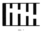
Fig. 7 illustrates a top view of another embodiment of the grid shapes in a CT detector according to the present invention. - Hereafter, a detailed description will be given for preferred embodiments of the present invention. It should be pointed out that in the detailed description of the embodiments, for simplicity and conciseness, it is impossible for the description to describe all the features of the practical embodiments in details. It should be understood that in the process of a practical implementation of any embodiment, just as in the process of an engineering project or a designing project, in order to achieve a specific goal of the developer and in order to satisfy some system-related or business-related constraints, a variety of decisions will usually be made, which will also be varied from one embodiment to another. In addition, it can also be understood that although the effort made in such developing process may be complex and time-consuming, some variations such as design, manufacture and production on the basis of the technical contents disclosed in the disclosure are just customary technical means in the art for those of ordinary skilled in the art relating to the contents disclosed in the present invention, which should not be regarded as insufficient disclosure of the present invention.
- Unless defined otherwise, all the technical or scientific terms used in the claims and the description should have the same meanings as commonly understood by one of ordinary skilled in the art to which the present invention belongs. The terms "first", "second" and the like in the description and the claims of the present application for invention do not mean any sequential order, number or importance, but are only used for distinguishing different components. The terms "a", "an" and the like do not denote a limitation of quantity, but denote the existence of at least one. The terms "comprises", "comprising", "includes", "including" and the like mean that the element or object in front of the "comprises", "comprising", "includes" and "including" encompasses the elements or objects and their equivalents illustrated following the "comprises", "comprising", "includes" and "including", but do not exclude other elements or objects. The term "coupled", "connected" or the like is not limited to being connected physically or mechanically, nor limited to being connected directly or indirectly.
- In order to make the purpose, the technical solutions and the advantages of the invention more apparent, the technical solutions of the present invention will be set forth clearly and fully hereinafter in combination with specific embodiments of the invention and the corresponding accompanying drawings. Obviously, the described embodiments are merely part-not all-of the embodiments in the present invention. In view of the embodiments in the present invention, other embodiments made by one of ordinary skilled in the art without inventive work all fall within the scope of protection of the invention.
- A CT detector usually includes multiple detector modules and multiple collimator plate.
Fig. 3 illustrates onedetector module 301 and thecorresponding collimator plate 302 in the CT detector. Thedetector module 301 includesmultiple scintillators 303 having gaps therebetween and for constituting two-dimensional discrete pixels, aphotoelectric receiving diode 304, and amodule pedestal 305. The scintillators may be arranged in the X direction and in the Z direction (along a vertical direction of a human body) to constitute a two-dimensional pixel array. Thephotoelectric receiving diode 304 may be mounted on themodule pedestal 305, and thescintillators 303 may be mounted on thephotoelectric receiving diode 304. Thecollimator plate 302 is located above one side of thedetector module 301 receiving X-rays, for guiding the X-rays to the corresponding two-dimensional discrete pixels. The upper edge of thecollimator plate 302 may be focused on a focus of a bulb tube of the X-rays, and the thickness of thecollimator plate 302 is in the X direction. - No matter for an arc detector or for a detector of a polyline-segment type, there are
certain gaps 306 between themultiple scintillators 303 within thedetector module 301. Therefore, in one embodiment of the present invention, as shown inFig. 3 in conjunction withFig. 4 ,grids 307 may also be provided between thedetector module 301 and thecollimator plate 302, used to block the X-rays emitted to thegaps 306. In one embodiment of the present invention, thegrids 307 may also be mounted on or above thescintillators 303. In one embodiment of the present invention, the lower edge of thecollimator plate 302 may be positioned on thegrids 307 or located above thegrids 307. - In one embodiment of the present invention, with reference to
Fig. 5 , thegrids 307 may be provided on the gaps in two intersecting directions. In conjunction withFig. 6 , thegrids 307 may be provided on the gaps in the X direction and in the Z direction, and may have a breaking joint on at least one gridline that is along the X direction. Similarly, there may also be a breaking joint on at least one gridline that is along the Z direction, or there may be breaking joints on at least one gridline that are along both the X direction and the Z direction. It should be emphasized that the positions of the breaking joints on different gridlines may be aligned, or may be not aligned. Although the breaking joints on the multiple gridlines that are along the X direction as shown inFig. 6 are aligned in the Z direction, the positions of these breaking joints may also be not aligned in the Z direction. - In another embodiment of the present invention, the
grids 307 may be provided on the gaps in only one direction. With reference toFig. 7 , thegrids 307 may be provided on the gaps only in the X direction, and may have breaking joints on at least one gridline that is along the X direction. - In one embodiment of the present invention, the grids may have a thickness between 80 micrometers and 10 millimeters.
- In one embodiment of the present invention, the gridlines in the grids themselves may have a width between 10 micrometers and 700 micrometers.
- In one embodiment of the present invention, two adjacent gridlines in the grids have a pitch between 0.08 millimeters and 3 millimeters.
- In one embodiment of the present invention, the grids may be made of a composite material containing tungsten or a high density alloy, or for strongly absorbing the X-rays.
- In one embodiment of the present invention, the gridlines may be provided on the gaps not only asymmetrically but also symmetrically. No matter the gridlines are symmetrically or asymmetrically provided, i.e. a criterion can both be satisfied that the gaps are ensured to be covered by the gridlines so as not to be irradiated by the X-rays. Moreover, when it is required to use the gridlines to eliminate crosstalk of the X-rays on the adjacent pixels, the gridlines may also cover areas on the adjacent pixels that may receive the crosstalk of the X-rays.
- So far a CT detector according to embodiments of the present invention has been described. According to the CT detector of the present invention, the X-rays can be prevented from entering the gaps between the adjacent pixels in the detector module, and the X-rays can be prevented from shifting to the adjacent pixels to produce crosstalk. In addition, the grids having the breaking joint are beneficial for the manufacture of the grids such that during the cutting process of the grids, a processing apparatus is capable of, after cutting out one blank, continuously moving into a next blank adjacent to the blank to process the next blank.
- Embodiments of the present invention have been described above, and are not used to limit the present invention. For those skilled in the art, various alterations and changes may be made to the present invention. In the spirit and the principle of the present invention, any modification, equivalents, improvement etc. made thereto all should fall within the scope of the claims of the present invention.
Claims (10)
- A CT detector (103), comprising:a detector module (301) that includes a plurality of scintillators (303) having gaps (306) therebetween and for constituting two-dimensional discrete pixels;a collimator plate (302) located above one side of said detector module (301) receiving X-rays, for guiding said X-rays to the corresponding two-dimensional discrete pixels;wherein the CT detector (103) further comprises:grids (307) located between said detector (301) module and said collimator plate (302), for blocking said X-rays emitted to said gaps (306).
- The CT detector (103) according to claim 1, wherein said grids (307) are provided on said gaps (306) in two intersecting directions, and have a breaking joint in at least one of said directions.
- The CT detector (103) according to any preceding claim, wherein said grids (304) are provided on said gaps (306) in one direction and have a breaking joint in said direction.
- The CT detector (103) according to any preceding claim, wherein said grids (307) have a thickness between 80 micrometers and 10 millimeters.
- The CT detector (103) according to any preceding claim, wherein gridlines in said grids (307) have a width between 10 micrometers and 700 micrometers.
- The CT detector (103) according to any preceding claim, wherein two adjacent gridlines in said grids (307) have a pitch between 0.08 millimeters and 3 millimeters.
- The CT detector (103) according to any preceding claim, wherein said grids (307) are made of a composite material containing tungsten or a high density alloy, or for strongly absorbing said X-rays.
- The CT detector (103) according to any preceding claim, wherein said grids (307) are asymmetrically provided on said gaps (306).
- The CT detector (103) according to any preceding claim, wherein said grids (307) are symmetrically provided on said gaps (306).
- The CT detector (103) according to any preceding claim, wherein said CT detector (103) includes a plurality of detector modules (301) being configured to be polyline-shaped.
Applications Claiming Priority (1)
| Application Number | Priority Date | Filing Date | Title |
|---|---|---|---|
| CN201410360281.1A CN105266835A (en) | 2014-07-25 | 2014-07-25 | CT detector |
Publications (2)
| Publication Number | Publication Date |
|---|---|
| EP2977792A1 true EP2977792A1 (en) | 2016-01-27 |
| EP2977792B1 EP2977792B1 (en) | 2018-06-13 |
Family
ID=53879306
Family Applications (1)
| Application Number | Title | Priority Date | Filing Date |
|---|---|---|---|
| EP15177549.1A Active EP2977792B1 (en) | 2014-07-25 | 2015-07-20 | A ct detector |
Country Status (4)
| Country | Link |
|---|---|
| US (1) | US20160025867A1 (en) |
| EP (1) | EP2977792B1 (en) |
| JP (1) | JP6548219B2 (en) |
| CN (1) | CN105266835A (en) |
Cited By (1)
| Publication number | Priority date | Publication date | Assignee | Title |
|---|---|---|---|---|
| CN115184256A (en) * | 2022-06-29 | 2022-10-14 | 武汉联影医疗科技有限公司 | Testing device and testing method for bulb tube, electronic device and storage medium |
Families Citing this family (6)
| Publication number | Priority date | Publication date | Assignee | Title |
|---|---|---|---|---|
| US10058293B2 (en) | 2016-02-19 | 2018-08-28 | Morpho Detection, Llc | Detector assemblies and methods for helical CT scanning |
| CN108121014A (en) * | 2017-12-07 | 2018-06-05 | 公安部第三研究所 | Perspective view scatters array detection system and method |
| CN108577880B (en) * | 2018-05-18 | 2022-05-27 | 上海联影医疗科技股份有限公司 | Anti-scatter grid and CT detection system |
| CN110123355B (en) * | 2019-05-30 | 2023-03-31 | 东软医疗系统股份有限公司 | Detection system |
| CN111067555A (en) * | 2019-12-25 | 2020-04-28 | 上海联影医疗科技有限公司 | CT detector |
| CN117064422B (en) * | 2023-09-13 | 2024-11-12 | 北京富通康影科技有限公司 | An anti-scattering grid for CT detector |
Citations (2)
| Publication number | Priority date | Publication date | Assignee | Title |
|---|---|---|---|---|
| US6304626B1 (en) * | 1998-10-20 | 2001-10-16 | Kabushiki Kaisha Toshiba | Two-dimensional array type of X-ray detector and computerized tomography apparatus |
| CN103135121A (en) * | 2011-11-28 | 2013-06-05 | Ge医疗系统环球技术有限公司 | Line segment type module computer tomography (CT) detector and method for eliminating crosstalk |
Family Cites Families (8)
| Publication number | Priority date | Publication date | Assignee | Title |
|---|---|---|---|---|
| DE10142531A1 (en) * | 2001-08-30 | 2003-03-20 | Philips Corp Intellectual Pty | Sensor arrangement of light and / or X-ray sensitive sensors |
| KR101125284B1 (en) * | 2010-02-03 | 2012-03-21 | 주식회사 디알텍 | X-ray grid and manufacturing method therefor |
| JP5660910B2 (en) * | 2010-03-30 | 2015-01-28 | 富士フイルム株式会社 | Method for manufacturing grid for radiographic imaging |
| DE102010020610A1 (en) * | 2010-05-14 | 2011-11-17 | Siemens Aktiengesellschaft | Radiation detector and method for producing a radiation detector |
| CN103222010A (en) * | 2010-10-08 | 2013-07-24 | 海龟湾合伙有限责任公司 | Three-dimensional focused anti-scatter grid and method for manufacturing thereof |
| JP5661486B2 (en) * | 2011-01-25 | 2015-01-28 | 株式会社日立メディコ | X-ray detector and X-ray CT apparatus provided with the same |
| DE102011103851B4 (en) * | 2011-05-26 | 2019-05-29 | Siemens Healthcare Gmbh | Grid module of a scattered radiation grid, modular scattered radiation grid, CT detector and CT system |
| JP2013040859A (en) * | 2011-08-17 | 2013-02-28 | Toshiba Corp | X-ray detector and x-ray ct apparatus |
-
2014
- 2014-07-25 CN CN201410360281.1A patent/CN105266835A/en active Pending
-
2015
- 2015-07-15 JP JP2015140930A patent/JP6548219B2/en active Active
- 2015-07-20 EP EP15177549.1A patent/EP2977792B1/en active Active
- 2015-07-24 US US14/807,906 patent/US20160025867A1/en not_active Abandoned
Patent Citations (2)
| Publication number | Priority date | Publication date | Assignee | Title |
|---|---|---|---|---|
| US6304626B1 (en) * | 1998-10-20 | 2001-10-16 | Kabushiki Kaisha Toshiba | Two-dimensional array type of X-ray detector and computerized tomography apparatus |
| CN103135121A (en) * | 2011-11-28 | 2013-06-05 | Ge医疗系统环球技术有限公司 | Line segment type module computer tomography (CT) detector and method for eliminating crosstalk |
Cited By (1)
| Publication number | Priority date | Publication date | Assignee | Title |
|---|---|---|---|---|
| CN115184256A (en) * | 2022-06-29 | 2022-10-14 | 武汉联影医疗科技有限公司 | Testing device and testing method for bulb tube, electronic device and storage medium |
Also Published As
| Publication number | Publication date |
|---|---|
| US20160025867A1 (en) | 2016-01-28 |
| CN105266835A (en) | 2016-01-27 |
| JP2016030215A (en) | 2016-03-07 |
| EP2977792B1 (en) | 2018-06-13 |
| JP6548219B2 (en) | 2019-07-24 |
Similar Documents
| Publication | Publication Date | Title |
|---|---|---|
| EP2977792B1 (en) | A ct detector | |
| EP3193720B1 (en) | Systems and methods for grating modulation of spectra and intensity in computed tomography | |
| DE102008004748A1 (en) | Method and apparatus for reducing charge sharing in pixellated, energy discriminating detectors | |
| US10045749B2 (en) | X-ray system, in particular a tomosynthesis system and a method for acquiring an image of an object | |
| US8976935B2 (en) | Collimator grid and an associated method of fabrication | |
| CN107427271A (en) | X-ray imaging device | |
| CN103135121B (en) | Line segment type module computer tomography (CT) detector and method for eliminating crosstalk | |
| DE102008003143A1 (en) | Laminated CT collimator and method of making the same | |
| CN202794067U (en) | Luggage CT safety inspection system and detector device thereof | |
| US11232881B2 (en) | Anti-scatter grid assembly for detector arrangement | |
| JP4510823B2 (en) | Device for collimating electromagnetic radiation | |
| CN104853679A (en) | Radiation beam intensity profile shaper | |
| CN105427914A (en) | Method for manufacturing a collimator module and method for manufacturing a collimator bridge as well as collimator module | |
| US9144408B2 (en) | Collimators for scan of radiation sources and methods of scanning | |
| CN102793557A (en) | Grid module, modular scattered-radiation grid, CT detector and CT system | |
| CN102793558B (en) | Grid module, modular scattered-radiation grid, CT detector and CT system | |
| JP5661486B2 (en) | X-ray detector and X-ray CT apparatus provided with the same | |
| JP6818592B2 (en) | Collimator, radiation detector, and radiation inspection equipment | |
| DE112015007248T5 (en) | DETECTOR ARRANGEMENT FOR RADIATION IMAGING METHOD | |
| KR101600976B1 (en) | X-ray grid | |
| WO2014136734A1 (en) | Radiation detector and x-ray ct device provided therewith | |
| US20170090046A1 (en) | X-ray detector arrangement | |
| JP6523451B2 (en) | Radiation detector and X-ray CT apparatus equipped with the same | |
| US11160517B2 (en) | Radiation imaging device | |
| DE102016125331B4 (en) | Matched flat panel X-ray detector, matched light imaging panel and method of making a light imaging panel |
Legal Events
| Date | Code | Title | Description |
|---|---|---|---|
| PUAI | Public reference made under article 153(3) epc to a published international application that has entered the european phase |
Free format text: ORIGINAL CODE: 0009012 |
|
| AK | Designated contracting states |
Kind code of ref document: A1 Designated state(s): AL AT BE BG CH CY CZ DE DK EE ES FI FR GB GR HR HU IE IS IT LI LT LU LV MC MK MT NL NO PL PT RO RS SE SI SK SM TR |
|
| AX | Request for extension of the european patent |
Extension state: BA ME |
|
| 17P | Request for examination filed |
Effective date: 20160727 |
|
| RBV | Designated contracting states (corrected) |
Designated state(s): AL AT BE BG CH CY CZ DE DK EE ES FI FR GB GR HR HU IE IS IT LI LT LU LV MC MK MT NL NO PL PT RO RS SE SI SK SM TR |
|
| GRAP | Despatch of communication of intention to grant a patent |
Free format text: ORIGINAL CODE: EPIDOSNIGR1 |
|
| INTG | Intention to grant announced |
Effective date: 20180209 |
|
| GRAS | Grant fee paid |
Free format text: ORIGINAL CODE: EPIDOSNIGR3 |
|
| GRAA | (expected) grant |
Free format text: ORIGINAL CODE: 0009210 |
|
| AK | Designated contracting states |
Kind code of ref document: B1 Designated state(s): AL AT BE BG CH CY CZ DE DK EE ES FI FR GB GR HR HU IE IS IT LI LT LU LV MC MK MT NL NO PL PT RO RS SE SI SK SM TR |
|
| REG | Reference to a national code |
Ref country code: GB Ref legal event code: FG4D |
|
| REG | Reference to a national code |
Ref country code: CH Ref legal event code: EP Ref country code: AT Ref legal event code: REF Ref document number: 1009062 Country of ref document: AT Kind code of ref document: T Effective date: 20180615 |
|
| REG | Reference to a national code |
Ref country code: IE Ref legal event code: FG4D |
|
| REG | Reference to a national code |
Ref country code: DE Ref legal event code: R096 Ref document number: 602015012144 Country of ref document: DE |
|
| REG | Reference to a national code |
Ref country code: NL Ref legal event code: MP Effective date: 20180613 |
|
| REG | Reference to a national code |
Ref country code: LT Ref legal event code: MG4D |
|
| PG25 | Lapsed in a contracting state [announced via postgrant information from national office to epo] |
Ref country code: NO Free format text: LAPSE BECAUSE OF FAILURE TO SUBMIT A TRANSLATION OF THE DESCRIPTION OR TO PAY THE FEE WITHIN THE PRESCRIBED TIME-LIMIT Effective date: 20180913 Ref country code: BG Free format text: LAPSE BECAUSE OF FAILURE TO SUBMIT A TRANSLATION OF THE DESCRIPTION OR TO PAY THE FEE WITHIN THE PRESCRIBED TIME-LIMIT Effective date: 20180913 Ref country code: LT Free format text: LAPSE BECAUSE OF FAILURE TO SUBMIT A TRANSLATION OF THE DESCRIPTION OR TO PAY THE FEE WITHIN THE PRESCRIBED TIME-LIMIT Effective date: 20180613 Ref country code: FI Free format text: LAPSE BECAUSE OF FAILURE TO SUBMIT A TRANSLATION OF THE DESCRIPTION OR TO PAY THE FEE WITHIN THE PRESCRIBED TIME-LIMIT Effective date: 20180613 Ref country code: SE Free format text: LAPSE BECAUSE OF FAILURE TO SUBMIT A TRANSLATION OF THE DESCRIPTION OR TO PAY THE FEE WITHIN THE PRESCRIBED TIME-LIMIT Effective date: 20180613 Ref country code: ES Free format text: LAPSE BECAUSE OF FAILURE TO SUBMIT A TRANSLATION OF THE DESCRIPTION OR TO PAY THE FEE WITHIN THE PRESCRIBED TIME-LIMIT Effective date: 20180613 Ref country code: CY Free format text: LAPSE BECAUSE OF FAILURE TO SUBMIT A TRANSLATION OF THE DESCRIPTION OR TO PAY THE FEE WITHIN THE PRESCRIBED TIME-LIMIT Effective date: 20180613 |
|
| PG25 | Lapsed in a contracting state [announced via postgrant information from national office to epo] |
Ref country code: RS Free format text: LAPSE BECAUSE OF FAILURE TO SUBMIT A TRANSLATION OF THE DESCRIPTION OR TO PAY THE FEE WITHIN THE PRESCRIBED TIME-LIMIT Effective date: 20180613 Ref country code: HR Free format text: LAPSE BECAUSE OF FAILURE TO SUBMIT A TRANSLATION OF THE DESCRIPTION OR TO PAY THE FEE WITHIN THE PRESCRIBED TIME-LIMIT Effective date: 20180613 Ref country code: LV Free format text: LAPSE BECAUSE OF FAILURE TO SUBMIT A TRANSLATION OF THE DESCRIPTION OR TO PAY THE FEE WITHIN THE PRESCRIBED TIME-LIMIT Effective date: 20180613 Ref country code: GR Free format text: LAPSE BECAUSE OF FAILURE TO SUBMIT A TRANSLATION OF THE DESCRIPTION OR TO PAY THE FEE WITHIN THE PRESCRIBED TIME-LIMIT Effective date: 20180914 |
|
| REG | Reference to a national code |
Ref country code: AT Ref legal event code: MK05 Ref document number: 1009062 Country of ref document: AT Kind code of ref document: T Effective date: 20180613 |
|
| PG25 | Lapsed in a contracting state [announced via postgrant information from national office to epo] |
Ref country code: NL Free format text: LAPSE BECAUSE OF FAILURE TO SUBMIT A TRANSLATION OF THE DESCRIPTION OR TO PAY THE FEE WITHIN THE PRESCRIBED TIME-LIMIT Effective date: 20180613 |
|
| PG25 | Lapsed in a contracting state [announced via postgrant information from national office to epo] |
Ref country code: AT Free format text: LAPSE BECAUSE OF FAILURE TO SUBMIT A TRANSLATION OF THE DESCRIPTION OR TO PAY THE FEE WITHIN THE PRESCRIBED TIME-LIMIT Effective date: 20180613 Ref country code: PL Free format text: LAPSE BECAUSE OF FAILURE TO SUBMIT A TRANSLATION OF THE DESCRIPTION OR TO PAY THE FEE WITHIN THE PRESCRIBED TIME-LIMIT Effective date: 20180613 Ref country code: IS Free format text: LAPSE BECAUSE OF FAILURE TO SUBMIT A TRANSLATION OF THE DESCRIPTION OR TO PAY THE FEE WITHIN THE PRESCRIBED TIME-LIMIT Effective date: 20181013 Ref country code: EE Free format text: LAPSE BECAUSE OF FAILURE TO SUBMIT A TRANSLATION OF THE DESCRIPTION OR TO PAY THE FEE WITHIN THE PRESCRIBED TIME-LIMIT Effective date: 20180613 Ref country code: CZ Free format text: LAPSE BECAUSE OF FAILURE TO SUBMIT A TRANSLATION OF THE DESCRIPTION OR TO PAY THE FEE WITHIN THE PRESCRIBED TIME-LIMIT Effective date: 20180613 Ref country code: RO Free format text: LAPSE BECAUSE OF FAILURE TO SUBMIT A TRANSLATION OF THE DESCRIPTION OR TO PAY THE FEE WITHIN THE PRESCRIBED TIME-LIMIT Effective date: 20180613 Ref country code: SK Free format text: LAPSE BECAUSE OF FAILURE TO SUBMIT A TRANSLATION OF THE DESCRIPTION OR TO PAY THE FEE WITHIN THE PRESCRIBED TIME-LIMIT Effective date: 20180613 |
|
| PG25 | Lapsed in a contracting state [announced via postgrant information from national office to epo] |
Ref country code: IT Free format text: LAPSE BECAUSE OF FAILURE TO SUBMIT A TRANSLATION OF THE DESCRIPTION OR TO PAY THE FEE WITHIN THE PRESCRIBED TIME-LIMIT Effective date: 20180613 Ref country code: SM Free format text: LAPSE BECAUSE OF FAILURE TO SUBMIT A TRANSLATION OF THE DESCRIPTION OR TO PAY THE FEE WITHIN THE PRESCRIBED TIME-LIMIT Effective date: 20180613 |
|
| REG | Reference to a national code |
Ref country code: CH Ref legal event code: PL |
|
| REG | Reference to a national code |
Ref country code: DE Ref legal event code: R097 Ref document number: 602015012144 Country of ref document: DE |
|
| PG25 | Lapsed in a contracting state [announced via postgrant information from national office to epo] |
Ref country code: LU Free format text: LAPSE BECAUSE OF NON-PAYMENT OF DUE FEES Effective date: 20180720 Ref country code: MC Free format text: LAPSE BECAUSE OF FAILURE TO SUBMIT A TRANSLATION OF THE DESCRIPTION OR TO PAY THE FEE WITHIN THE PRESCRIBED TIME-LIMIT Effective date: 20180613 |
|
| REG | Reference to a national code |
Ref country code: BE Ref legal event code: MM Effective date: 20180731 |
|
| REG | Reference to a national code |
Ref country code: IE Ref legal event code: MM4A |
|
| PLBE | No opposition filed within time limit |
Free format text: ORIGINAL CODE: 0009261 |
|
| STAA | Information on the status of an ep patent application or granted ep patent |
Free format text: STATUS: NO OPPOSITION FILED WITHIN TIME LIMIT |
|
| PG25 | Lapsed in a contracting state [announced via postgrant information from national office to epo] |
Ref country code: CH Free format text: LAPSE BECAUSE OF NON-PAYMENT OF DUE FEES Effective date: 20180731 Ref country code: IE Free format text: LAPSE BECAUSE OF NON-PAYMENT OF DUE FEES Effective date: 20180720 Ref country code: LI Free format text: LAPSE BECAUSE OF NON-PAYMENT OF DUE FEES Effective date: 20180731 |
|
| 26N | No opposition filed |
Effective date: 20190314 |
|
| PG25 | Lapsed in a contracting state [announced via postgrant information from national office to epo] |
Ref country code: SI Free format text: LAPSE BECAUSE OF FAILURE TO SUBMIT A TRANSLATION OF THE DESCRIPTION OR TO PAY THE FEE WITHIN THE PRESCRIBED TIME-LIMIT Effective date: 20180613 Ref country code: DK Free format text: LAPSE BECAUSE OF FAILURE TO SUBMIT A TRANSLATION OF THE DESCRIPTION OR TO PAY THE FEE WITHIN THE PRESCRIBED TIME-LIMIT Effective date: 20180613 Ref country code: BE Free format text: LAPSE BECAUSE OF NON-PAYMENT OF DUE FEES Effective date: 20180731 |
|
| PG25 | Lapsed in a contracting state [announced via postgrant information from national office to epo] |
Ref country code: FR Free format text: LAPSE BECAUSE OF NON-PAYMENT OF DUE FEES Effective date: 20180813 |
|
| PG25 | Lapsed in a contracting state [announced via postgrant information from national office to epo] |
Ref country code: AL Free format text: LAPSE BECAUSE OF FAILURE TO SUBMIT A TRANSLATION OF THE DESCRIPTION OR TO PAY THE FEE WITHIN THE PRESCRIBED TIME-LIMIT Effective date: 20180613 |
|
| PG25 | Lapsed in a contracting state [announced via postgrant information from national office to epo] |
Ref country code: MT Free format text: LAPSE BECAUSE OF NON-PAYMENT OF DUE FEES Effective date: 20180720 |
|
| PG25 | Lapsed in a contracting state [announced via postgrant information from national office to epo] |
Ref country code: TR Free format text: LAPSE BECAUSE OF FAILURE TO SUBMIT A TRANSLATION OF THE DESCRIPTION OR TO PAY THE FEE WITHIN THE PRESCRIBED TIME-LIMIT Effective date: 20180613 |
|
| PG25 | Lapsed in a contracting state [announced via postgrant information from national office to epo] |
Ref country code: PT Free format text: LAPSE BECAUSE OF FAILURE TO SUBMIT A TRANSLATION OF THE DESCRIPTION OR TO PAY THE FEE WITHIN THE PRESCRIBED TIME-LIMIT Effective date: 20180613 |
|
| PG25 | Lapsed in a contracting state [announced via postgrant information from national office to epo] |
Ref country code: MK Free format text: LAPSE BECAUSE OF NON-PAYMENT OF DUE FEES Effective date: 20180613 Ref country code: HU Free format text: LAPSE BECAUSE OF FAILURE TO SUBMIT A TRANSLATION OF THE DESCRIPTION OR TO PAY THE FEE WITHIN THE PRESCRIBED TIME-LIMIT; INVALID AB INITIO Effective date: 20150720 |
|
| P01 | Opt-out of the competence of the unified patent court (upc) registered |
Effective date: 20230528 |
|
| PGFP | Annual fee paid to national office [announced via postgrant information from national office to epo] |
Ref country code: GB Payment date: 20250619 Year of fee payment: 11 |
|
| PGFP | Annual fee paid to national office [announced via postgrant information from national office to epo] |
Ref country code: DE Payment date: 20250620 Year of fee payment: 11 |