EP2975546A1 - Systems and methods for verifying the authenticity of an applicatiotn during execution - Google Patents
Systems and methods for verifying the authenticity of an applicatiotn during execution Download PDFInfo
- Publication number
- EP2975546A1 EP2975546A1 EP15175920.6A EP15175920A EP2975546A1 EP 2975546 A1 EP2975546 A1 EP 2975546A1 EP 15175920 A EP15175920 A EP 15175920A EP 2975546 A1 EP2975546 A1 EP 2975546A1
- Authority
- EP
- European Patent Office
- Prior art keywords
- application
- electronic device
- processing circuitry
- check routine
- authenticity check
- Prior art date
- Legal status (The legal status is an assumption and is not a legal conclusion. Google has not performed a legal analysis and makes no representation as to the accuracy of the status listed.)
- Granted
Links
Images
Classifications
-
- G—PHYSICS
- G06—COMPUTING OR CALCULATING; COUNTING
- G06F—ELECTRIC DIGITAL DATA PROCESSING
- G06F21/00—Security arrangements for protecting computers, components thereof, programs or data against unauthorised activity
- G06F21/50—Monitoring users, programs or devices to maintain the integrity of platforms, e.g. of processors, firmware or operating systems
- G06F21/52—Monitoring users, programs or devices to maintain the integrity of platforms, e.g. of processors, firmware or operating systems during program execution, e.g. stack integrity ; Preventing unwanted data erasure; Buffer overflow
-
- G—PHYSICS
- G06—COMPUTING OR CALCULATING; COUNTING
- G06F—ELECTRIC DIGITAL DATA PROCESSING
- G06F21/00—Security arrangements for protecting computers, components thereof, programs or data against unauthorised activity
- G06F21/10—Protecting distributed programs or content, e.g. vending or licensing of copyrighted material ; Digital rights management [DRM]
- G06F21/12—Protecting executable software
- G06F21/121—Restricting unauthorised execution of programs
-
- G—PHYSICS
- G06—COMPUTING OR CALCULATING; COUNTING
- G06F—ELECTRIC DIGITAL DATA PROCESSING
- G06F21/00—Security arrangements for protecting computers, components thereof, programs or data against unauthorised activity
- G06F21/50—Monitoring users, programs or devices to maintain the integrity of platforms, e.g. of processors, firmware or operating systems
- G06F21/55—Detecting local intrusion or implementing counter-measures
- G06F21/552—Detecting local intrusion or implementing counter-measures involving long-term monitoring or reporting
-
- G—PHYSICS
- G06—COMPUTING OR CALCULATING; COUNTING
- G06F—ELECTRIC DIGITAL DATA PROCESSING
- G06F21/00—Security arrangements for protecting computers, components thereof, programs or data against unauthorised activity
- G06F21/50—Monitoring users, programs or devices to maintain the integrity of platforms, e.g. of processors, firmware or operating systems
- G06F21/57—Certifying or maintaining trusted computer platforms, e.g. secure boots or power-downs, version controls, system software checks, secure updates or assessing vulnerabilities
- G06F21/575—Secure boot
-
- G—PHYSICS
- G06—COMPUTING OR CALCULATING; COUNTING
- G06F—ELECTRIC DIGITAL DATA PROCESSING
- G06F21/00—Security arrangements for protecting computers, components thereof, programs or data against unauthorised activity
- G06F21/60—Protecting data
- G06F21/62—Protecting access to data via a platform, e.g. using keys or access control rules
-
- G—PHYSICS
- G06—COMPUTING OR CALCULATING; COUNTING
- G06F—ELECTRIC DIGITAL DATA PROCESSING
- G06F21/00—Security arrangements for protecting computers, components thereof, programs or data against unauthorised activity
- G06F21/70—Protecting specific internal or peripheral components, in which the protection of a component leads to protection of the entire computer
- G06F21/71—Protecting specific internal or peripheral components, in which the protection of a component leads to protection of the entire computer to assure secure computing or processing of information
- G06F21/76—Protecting specific internal or peripheral components, in which the protection of a component leads to protection of the entire computer to assure secure computing or processing of information in application-specific integrated circuits [ASIC] or field-programmable devices, e.g. field-programmable gate arrays [FPGA] or programmable logic devices [PLD]
-
- G—PHYSICS
- G06—COMPUTING OR CALCULATING; COUNTING
- G06F—ELECTRIC DIGITAL DATA PROCESSING
- G06F9/00—Arrangements for program control, e.g. control units
- G06F9/06—Arrangements for program control, e.g. control units using stored programs, i.e. using an internal store of processing equipment to receive or retain programs
- G06F9/44—Arrangements for executing specific programs
- G06F9/445—Program loading or initiating
-
- G—PHYSICS
- G06—COMPUTING OR CALCULATING; COUNTING
- G06Q—INFORMATION AND COMMUNICATION TECHNOLOGY [ICT] SPECIALLY ADAPTED FOR ADMINISTRATIVE, COMMERCIAL, FINANCIAL, MANAGERIAL OR SUPERVISORY PURPOSES; SYSTEMS OR METHODS SPECIALLY ADAPTED FOR ADMINISTRATIVE, COMMERCIAL, FINANCIAL, MANAGERIAL OR SUPERVISORY PURPOSES, NOT OTHERWISE PROVIDED FOR
- G06Q30/00—Commerce
- G06Q30/018—Certifying business or products
-
- G—PHYSICS
- G06—COMPUTING OR CALCULATING; COUNTING
- G06Q—INFORMATION AND COMMUNICATION TECHNOLOGY [ICT] SPECIALLY ADAPTED FOR ADMINISTRATIVE, COMMERCIAL, FINANCIAL, MANAGERIAL OR SUPERVISORY PURPOSES; SYSTEMS OR METHODS SPECIALLY ADAPTED FOR ADMINISTRATIVE, COMMERCIAL, FINANCIAL, MANAGERIAL OR SUPERVISORY PURPOSES, NOT OTHERWISE PROVIDED FOR
- G06Q50/00—Information and communication technology [ICT] specially adapted for implementation of business processes of specific business sectors, e.g. utilities or tourism
- G06Q50/06—Energy or water supply
-
- H—ELECTRICITY
- H04—ELECTRIC COMMUNICATION TECHNIQUE
- H04W—WIRELESS COMMUNICATION NETWORKS
- H04W12/00—Security arrangements; Authentication; Protecting privacy or anonymity
- H04W12/12—Detection or prevention of fraud
- H04W12/128—Anti-malware arrangements, e.g. protection against SMS fraud or mobile malware
-
- H—ELECTRICITY
- H04—ELECTRIC COMMUNICATION TECHNIQUE
- H04W—WIRELESS COMMUNICATION NETWORKS
- H04W4/00—Services specially adapted for wireless communication networks; Facilities therefor
- H04W4/60—Subscription-based services using application servers or record carriers, e.g. SIM application toolkits
-
- G—PHYSICS
- G06—COMPUTING OR CALCULATING; COUNTING
- G06F—ELECTRIC DIGITAL DATA PROCESSING
- G06F2221/00—Indexing scheme relating to security arrangements for protecting computers, components thereof, programs or data against unauthorised activity
- G06F2221/03—Indexing scheme relating to G06F21/50, monitoring users, programs or devices to maintain the integrity of platforms
- G06F2221/033—Test or assess software
-
- G—PHYSICS
- G06—COMPUTING OR CALCULATING; COUNTING
- G06F—ELECTRIC DIGITAL DATA PROCESSING
- G06F2221/00—Indexing scheme relating to security arrangements for protecting computers, components thereof, programs or data against unauthorised activity
- G06F2221/21—Indexing scheme relating to G06F21/00 and subgroups addressing additional information or applications relating to security arrangements for protecting computers, components thereof, programs or data against unauthorised activity
- G06F2221/2107—File encryption
-
- H—ELECTRICITY
- H04—ELECTRIC COMMUNICATION TECHNIQUE
- H04L—TRANSMISSION OF DIGITAL INFORMATION, e.g. TELEGRAPHIC COMMUNICATION
- H04L63/00—Network architectures or network communication protocols for network security
- H04L63/08—Network architectures or network communication protocols for network security for authentication of entities
- H04L63/0823—Network architectures or network communication protocols for network security for authentication of entities using certificates
-
- H—ELECTRICITY
- H04—ELECTRIC COMMUNICATION TECHNIQUE
- H04L—TRANSMISSION OF DIGITAL INFORMATION, e.g. TELEGRAPHIC COMMUNICATION
- H04L63/00—Network architectures or network communication protocols for network security
- H04L63/12—Applying verification of the received information
- H04L63/123—Applying verification of the received information received data contents, e.g. message integrity
-
- H—ELECTRICITY
- H04—ELECTRIC COMMUNICATION TECHNIQUE
- H04W—WIRELESS COMMUNICATION NETWORKS
- H04W12/00—Security arrangements; Authentication; Protecting privacy or anonymity
- H04W12/10—Integrity
-
- Y—GENERAL TAGGING OF NEW TECHNOLOGICAL DEVELOPMENTS; GENERAL TAGGING OF CROSS-SECTIONAL TECHNOLOGIES SPANNING OVER SEVERAL SECTIONS OF THE IPC; TECHNICAL SUBJECTS COVERED BY FORMER USPC CROSS-REFERENCE ART COLLECTIONS [XRACs] AND DIGESTS
- Y02—TECHNOLOGIES OR APPLICATIONS FOR MITIGATION OR ADAPTATION AGAINST CLIMATE CHANGE
- Y02D—CLIMATE CHANGE MITIGATION TECHNOLOGIES IN INFORMATION AND COMMUNICATION TECHNOLOGIES [ICT], I.E. INFORMATION AND COMMUNICATION TECHNOLOGIES AIMING AT THE REDUCTION OF THEIR OWN ENERGY USE
- Y02D10/00—Energy efficient computing, e.g. low power processors, power management or thermal management
-
- Y—GENERAL TAGGING OF NEW TECHNOLOGICAL DEVELOPMENTS; GENERAL TAGGING OF CROSS-SECTIONAL TECHNOLOGIES SPANNING OVER SEVERAL SECTIONS OF THE IPC; TECHNICAL SUBJECTS COVERED BY FORMER USPC CROSS-REFERENCE ART COLLECTIONS [XRACs] AND DIGESTS
- Y04—INFORMATION OR COMMUNICATION TECHNOLOGIES HAVING AN IMPACT ON OTHER TECHNOLOGY AREAS
- Y04S—SYSTEMS INTEGRATING TECHNOLOGIES RELATED TO POWER NETWORK OPERATION, COMMUNICATION OR INFORMATION TECHNOLOGIES FOR IMPROVING THE ELECTRICAL POWER GENERATION, TRANSMISSION, DISTRIBUTION, MANAGEMENT OR USAGE, i.e. SMART GRIDS
- Y04S40/00—Systems for electrical power generation, transmission, distribution or end-user application management characterised by the use of communication or information technologies, or communication or information technology specific aspects supporting them
- Y04S40/20—Information technology specific aspects, e.g. CAD, simulation, modelling, system security
Definitions
- the subject matter disclosed herein relates to electronic processing devices, and, more specifically to verifying the authenticity of instructions being executed by a processor of an electronic device.
- Certain modem electronic devices such as cellular phones, digital video recorders, console gaming systems, and so forth, generally include processing circuitry that executes instructions stored in memory in order for the electronic device to function as intended.
- certain electronic devices may store and execute firmware instructions that generally define the behavior of the electronic device.
- these firmware instructions may be stored in the memory of the electronic device at the time the electronic device is manufactured. Additionally, in certain situations, the firmware may be updated over the lifetime of the electronic device to address firmware bugs and/or to augment functionality of the electronic device.
- a system in an embodiment, includes an electronic device having memory circuitry configured to store an application comprising a plurality of instructions.
- the system also includes processing circuitry configured to execute the application and an application authenticity check routine, wherein the application authenticity check routine includes instructions executable by the processing circuitry to use idle processing time to verify an authenticity of the application throughout execution of the application.
- a method in another embodiment, includes instructing processing circuitry of an electronic device to initiate execution of an application stored in a memory of the electronic device. The method includes executing the application while executing an authenticity check routine using the processor of the electronic device, wherein the authenticity check routine comprises a plurality of instructions configured to cause the processing circuitry to determine whether the application has been modified subsequent to packaging.
- a non-transitory, computer-readable medium stores instructions executable by at least one processor of an electronic device.
- the instructions include instructions to execute an application stored in at least one memory of the electronic device and instructions to intermittently execute an authenticity check routine while executing the application.
- the authenticity check routine includes instructions to compute a digest value for the application stored in the at least one memory of the electronic device and instructions to decrypt a portion of the application stored in the at least one memory of the electronic device to determine a stored digest value for the application.
- the instructions also include instructions to determine that the application is authentic whenever the at least one processor determines that the computed digest value is equal to the stored digest value.
- modem electronic devices store or encode a set of instructions (e.g., applications, modules, routines, firmware, or any other suitable instructions) that are executed by processing circuitry to enable the electronic device to provide its intended functionality.
- electronic devices may operate for extended periods of time without interruption (e.g., without power cycling or rebooting) after installation and/or activation.
- an industrial monitoring and/or control system may generally include a number of field devices (e.g., sensing devices, relays, actuators, and so forth), which may be deployed throughout a facility and may subsequently operate for an extended period of time (e.g., months to years) after deployment without interruption.
- these field devices may generally operate by executing instructions, such as executable applications that are stored in a memory circuitry of the device prior to deployment.
- instructions such as executable applications that are stored in a memory circuitry of the device prior to deployment.
- the instructions stored within the memory circuitry of an electronic device are modified, the behavior and functionality of the device will also be modified.
- present embodiments enable an electronic device to perform an initial check that verifies the authenticity of stored instructions (e.g., firmware) before execution, such as during a booting sequence.
- stored instructions e.g., firmware
- a set of instructions is considered “authentic” if the instructions have not been modified after packaging (e.g., assembling, bundling) by the manufacturer or another authorized software provider.
- present embodiments also provide a mechanism whereby the authenticity of the stored application packages may be continually, regularly, or sporadically verified during execution of the stored applications.
- the instructions in an executable application may include an authenticity check routine that is continually, regularly, or sporadically executed by the processing circuitry of the electronic device to determine whether the application has been modified subsequent to packaging.
- the authenticity check routine may be executed by the processing circuitry of the electronic device during otherwise idle processing time, rendering the electronic device more robust to thwart differential power analysis and/or electromagnetic (EM) noise analysis techniques.
- the authenticity check routine may be performed using specialized processing circuitry, such as a high-security module (HSM) or a field-programmable gate array (FPGA) (e.g., a hardware accelerator). Accordingly, present embodiments enable the continual, regular, or sporadic authenticity verification of an application, even as it is actively being executed by the electronic device.
- HSM high-security module
- FPGA field-programmable gate array
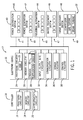
- FIG. 1 is a schematic of an electronic device 10, in accordance with an embodiment of the present approach.
- the electronic device 10 may be a consumer device (e.g., a cellular telephone, a tablet computing device, a portable computing device, a desktop computing device, a digital video recorder, a video game console device, a television) or an industrial device (e.g., a relay, an intelligent electronic device (IED), a field device, an end device).
- the electronic device 10 illustrated in FIG. 1 is an embodiment of an intelligent electronic device (IED) 10 that is part of an industrial monitoring and/or control system 12.
- the industrial equipment 22 may include a power distribution system 40 having various power distribution components 41 (e.g., transformers, transmission lines, capacitor banks, etc.), a power generation system 42 having various power generation components 43 (e.g., generators, combustors, engines, etc.), an industrial automation system 44 with various automation components 45 (e.g., reactors, conveyor belts, feeders, hoppers, etc.), a water treatment system 46 having various water treatment components 47 (e.g., filters, clarifiers, pH gauges, etc.), and/or a turbomachinery system 48 having various turbomachine components (e.g., turbines, combustors, compressors, etc.).
- various power distribution components 41 e.g., transformers, transmission lines, capacitor banks, etc.
- a power generation system 42 having various power generation components 43 (e.g., generators, combustors, engines, etc.)
- an industrial automation system 44 with various automation components 45 e.g., reactors, conveyor belts, feeders,
- the illustrated controller 14 generally includes processing circuitry 16, memory circuitry 18, and communication circuitry 20 to enable the controller 14 to manage the industrial monitoring and/or control system 12.
- the illustrated industrial equipment 22 are merely provided as examples of pieces of equipment that may be monitored and/or controlled by the electronic device 10 and the controller 14 of the industrial control and/or monitoring system 12, and that any other suitable piece of equipment (e.g., a combustor, a blower, a reactor, etc.) may be monitored and/or controlled by the industrial control and/or monitoring system 12 in accordance with the present disclosure.
- the illustrated electronic device 10 includes processing circuitry 24 (e.g., a general purpose microprocessor, an application-specific integrated circuit (ASIC), or other suitable processing circuitry) that is capable of executing instructions (e.g., executable applications, modules, routines, firmware, and so forth) to provide the desired functionality and behavior of the electronic device 10.
- this processing circuitry 24 may include a high-security module (HSM) 25, discussed in greater detail below, which may enable enhanced security during certain processing activities.
- this processing circuitry 24 may include a field-programmable gate array (FPGA) device, such as a hardware accelerator, that may be programmed when the device is manufactured to perform certain processing tasks during operation of the electronic device 10.
- FPGA field-programmable gate array
- the FPGA may be configured or programmed at a hardware-level at the time that the electronic device 10 is manufactured based on instructions (e.g., software code), such that the FPGA performs the functions described by the instructions during operation. Accordingly, for such embodiments, since the instructions are used to program the FPGA, and since these instructions are carried out by the FPGA during operation, the FPGA may be described herein as storing and executing instructions.
- instructions e.g., software code
- the illustrated electronic device 10 includes memory circuitry 26 (e.g., electrically erasable programmable read-only memory (EEPROM), a solid state disk drive, a flash drive, or another suitable non-volatile data storage mechanism) capable of storing the aforementioned instructions for execution by the processing circuitry 24.
- the memory circuitry 26 stores a package 27 (e.g., software package 27) that, as discussed in greater detail below, includes an executable application 28 (e.g., software 28) as well as a digest value 30 associated with the executable application 28.
- an application is a set of encoded instructions (e.g., binary encoded instructions) that are executable by the processing circuitry 24 of the electronic device 10.
- the illustrated electronic device 10 includes input/output (I/O) circuitry 32 capable of receiving user input via one or more input devices (e.g., touchscreens, pointing devices, keyboards, microphones, accelerometers, and so forth) and/or providing output to the user via one or more output devices (e.g., displays, touchscreens, speakers, indicator lights, printers, and so forth).
- the illustrated electronic device 10 includes communication circuitry 34 (e.g., a wired or wireless network interface card (NIC)) to enable the electronic device 10 to communicate with other electronic devices (e.g., the controller 14) via a network (e.g., via a local network or via the internet).
- NIC network interface card
- the illustrated electronic device 10 includes sensor circuitry 36 that enables the electronic device 10 to collect sensory information regarding the performance of the industrial equipment 22.
- the sensor circuitry 36 may include, for example, temperature sensors, pressure sensors, flow sensors, composition sensors (e.g., gas composition sensors, oxygen sensors, exhaust gas sensors, etc.), flame sensors, positional sensors, clearance sensors, vibration sensors, accelerometers, rotational speed sensors, voltage sensors, amperage sensors, frequency sensors, light sensors, sound sensors, or any other suitable sensing elements.
- the sensor circuitry 36 may include a rotational speed sensor that may be capable of measuring the speed of the turbomachinery 49 (e.g., a drive system of a compressor, a gas turbine, or a steam turbine).
- the processing circuitry 24 may execute a routine of the application 28 stored in the memory circuitry 26 of the electronic device 10 to determine the speed of the turbomachinery 49 based on measurements collected by the sensor circuitry 36. Further, the electronic device 10 may provide the determined speed of the turbomachinery 49 to the controller 14, via the communication circuitry 34, such that the processor 16 of the controller 14 may determine the operation parameters or state of the turbomachinery 49, as well as other portions of the industrial control and/or monitoring system 12.
- the illustrated electronic device 10 also includes control circuitry 38 that enables the electronic device 10 provide control signals to the turbomachinery 49 to modulate the performance of the turbomachinery 49 based on instructions from the controller 14.
- the control circuitry 38 may provide output signals that result in either an increase or a decrease in power being supplied to a drive system of a compressor of the turbomachinery system 48, modulating the performance of the compressor. More specifically, if the controller 14 determines that the output of the compressor is too low based on measurements collected by the sensor circuitry 36, then the controller 14 may, via the communication circuitry 34, instruct the electronic device 10 to increase the output of the compressor. In response, the electronic device 10, using the control circuitry 38, may provide control signals to the drive system of the compressor to increase the power supplied to the drive system, thereby increasing the output of the compressor.
- the executable applications 28 may be stored in the memory circuitry 16 at the time the electronic device 10 is manufactured and may be updated thereafter to address errors or bugs in the instructions 14 and/or to augment functionality of the electronic device 10.
- the modification of the executable application 28 in the memory circuitry 26 of the electronic device 10. One possibility is simple data corruption, wherein a hardware glitch, a cosmic ray collision, or another similar event results in a change (e.g., a single bit swap) in the executable application 28 stored in the memory circuitry 26.
- an unauthorized party may intentionally try to alter one or more bits of data in the executable application 28 in an attempt to cause an exception (e.g., a fault) in the electronic device 10, or in an attempt to gain unauthorized access to the electronic device 10. If the unauthorized party can gain physical access to the electronic device 10, this data alteration might be accomplished, for example, by polishing down the integrated circuit (IC) packaging of the memory circuitry 26, and then providing electromagnetic radiation (e.g., laser light) to specific physical locations to alter one or more bits stored in the memory circuitry 26.
- IC integrated circuit
- electromagnetic radiation e.g., laser light
- present embodiments provide a mechanism to verify the authenticity of the application 28 throughout execution of the application 28. That is, rather than only verifying the authenticity of an application before it is executed (e.g., during bootup), present embodiments are able to identify and address even single bit changes to the contents of the application 28 that may occur at any point during the execution of the application 28. Further, it may be noted that the success of the EM attack described above is greater when the unauthorized party can ascertain where (in the memory circuitry 26 and/or the processing circuitry 24) or when (during operation of the electronic device 10) to attack the circuitry of the electronic device 10. As such, certain presently disclosed embodiments enable the processing circuitry 24 of the electronic device 10 to continually be active, continually verifying the authenticity of the application 28, which makes it more difficult for an unauthorized party to plan and implement an attack, rendering the electronic device 10 more secure.
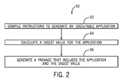
- FIG. 2 is a flow diagram that depicts an embodiment of a computer-implemented process 50 whereby an authorized software provider, such as the manufacturer of the electronic device 10, may generate a package 27 (e.g., a software package 27) for installation in the memory circuitry 26 of the electronic device 10.
- the illustrated process 50 begins with the authorized software provider compiling (block 52) instructions to generate an executable application 28.
- a set of human-readable code written in a programming language e.g., C, C++, Ada, Fortran
- a programming language e.g., C, C++, Ada, Fortran
- a digest value may be calculated (block 54) for the application compiled in block 52. That is, using a suitable processing device, the executable application 28 generated in block 52 may be provided as input to an algorithm that outputs a digest value 30.
- the digest value 30 may generally be a cryptographic hash value that is computed (e.g., generated or determined) using a cryptographic hash function (e.g., MD4, MD5, SHA-1, SHA-2, SHA-3, SHA-256).
- the digest value 30 may generally include a fixed-length string that is generated from a bit-wise digestion of the application 28, such that even a single bit difference in the input (e.g., the application 28) yields different digest value 30.
- a package 27 (e.g., a software package 27) may be generated (block 56) that includes the application 30 generated in block 52 as well as the digest value 30 generated in block 54.
- the package 27 may be a file container (e.g., a zip file, a tar file) that includes a binary executable application file 30 and a text file that includes the digest value 30.
- the package 27 may be compressed such that the package 27 occupies less space in the memory circuitry 26 of the electronic device 10. Further, in certain embodiments, the package 27 may be entirely or partially encrypted.
- a suitable processing device may use an encryption key that is associated with the manufacturer of the electronic device 10, or an encryption key associated with an authorized software provider, to encrypt some or all of the package 27.
- the entire package 27 may be encrypted.
- the application 28 and the digest value 30 stored within the package 27 may be individually encrypted.
- the digest value 30 alone may be encrypted before being included in the package 27.
- the encryption key used by the manufacturer or the authorized software provider to encrypt the package 27 are associated with corresponding decryption keys stored within the memory circuitry 26 of the electronic device 10, for example, at the time of manufacturing.
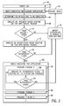
- FIG. 3 is a flow diagram illustrating an embodiment of a process 60 in which the electronic device 10 boots, verifies, and conditionally executes an application.
- the illustrated process 60 begins as the electronic device 10 is powered on (block 62). After powering on, the electronic device 10 may, in certain embodiments, perform one or more checks (e.g., a memory check of the memory circuitry 26, a voltage check of the processing circuitry 24) to verify the proper operation of the hardware components of the electronic device before proceeding.
- the processing circuitry 24 of the electronic device 10 may begin executing a bootloader application (block 64).
- the bootloader application may be a collection of instructions stored in the memory circuitry 26 and executable by the processing circuitry 24 of the electronic device 10 that enable an application to be selected, verified, and conditionally executed.
- the processing circuitry 24 of the electronic device 10 executing the bootloader application may then determine (block 66) an application, stored in the memory circuitry 26, to be executed. For example, in certain embodiments, the bootloader application may prompt a user (e.g., using the I/O circuitry 32 discussed above) to select a particular application 28 stored in the memory circuitry 26 for execution. In other embodiments, the bootloader application may automatically select an application 28 to execute based on identifying information associated with the application 28 (e.g., name, size, version, or location in the memory circuitry 26).
- identifying information associated with the application 28 e.g., name, size, version, or location in the memory circuitry 26.
- an integrity check routine on the package 27, which includes the application 28.
- the integrity check routine may be part of the bootloader application, or may be a separate routine called by the bootloader application.
- an integrity check is a high-level check that generally ensures that the package 27 likely includes a legitimate application, but does not involve a bit-wise analysis of the contents of the package 27 or the application 28.
- the integrity check may ensure that the package 27 is the appropriate file type (e.g., a zip file, or a tar file), that the package 27 includes a binary executable file 28 and a digest value 30, that the package 27 is the correct file size, that the package 27 conforms to the proper file naming standards, or other high-level checks.
- the integrity check routine may involve the computation and comparison of a checksum value (e.g., a cyclic redundancy check (CRC)) to verify the integrity of the package 27, as well as the application 28 stored therein.
- a checksum value e.g., a cyclic redundancy check (CRC)
- the processing circuitry 24 of the electronic device may modify (block 72) the application 28 and/or the application package 27 to render it non-bootable. For example, if the integrity check routine of a bootloader application determines that the package 27 or the application 28 lacks integrity, then the bootloader application may modify the contents of the package 27 and/or the application 28 (e.g., insert a flag, modify the value of one or more bits, or erase the package 27 altogether) such that the bootloader will not attempt to execute the application 28 again. Subsequently, the bootloader causes the electronic device 10 to perform a system reset (block 74), enabling the electronic device to begin executing the bootloader application anew (block 64).
- a system reset block 74
- the processing circuitry 24 may then execute (block 76) an authenticity check routine on the package 27, which includes the application 28.
- an authenticity check routine is discussed in detail below with respect to FIG. 4 .
- the authenticity check routine of block 76 may be part of the bootloader application, or may be a separate routine called by the bootloader application. Regardless, as set forth below, the authenticity check routine generally performs a bit-wise analysis of the application 28 stored in the package 27 to determine if the application 28 matches the digest value 30 also stored in the package 27.
- the processing circuitry 24 may modify (block 72) the package 27 and/or the application 28 to render it un-bootable and initiate a system reset (block 74).
- the modification (block 72) of the application may be skipped when an application fails an integrity or authenticity check (e.g., blocks 70, 78, or 88), and the device may instead proceed directly to the system reset (block 74), which effectively prevents the device from executing the application in question without the modification of block 72.
- the processing circuitry 24 may begin executing the application 28 (block 80). As illustrated in FIG. 3 , during execution, the application 28 spawns an initial thread or process 82 (e.g., thread or process 0) in addition to other threads or processes 84 and 86. Additionally, in executing the initial thread 82 of the application 28, the processing circuitry 24 of the electronic device 10 may execute (block 88) an authenticity routine to again verify the authenticity of the package 27 and the application 28. In other words, in certain embodiments, the application 28 includes an authenticity check routine that instructs the processing circuitry 24 of the electronic device 10 to verify the authenticity of the application 28 currently being executed. An example of an authenticity check routine is discussed in detail below with respect to FIG.
- the processing circuitry 24 may include multiple processing units (e.g., processing cores), and a particular processing unit may be used or dedicated to the execution of the authenticity check routine of blocks 76 and/or 88.
- the processing circuitry 24 may include a HSM that executes the authenticity check routine.
- the authenticity check routine may be stored separately (e.g., in a separate memory device or a separate memory location) from the application 28.
- the authenticity check routine may be performed by a hardware accelerator (e.g., a FPGA) that stores and executes instructions to perform an authenticity check routine of the application 28.
- the authenticity check routine generally performs a bit-wise analysis of the application 28 stored in the package 27 to determine if the application 28 still matches the digest value 30 also stored in the package 27.
- the authenticity check routine of blocks 78 and 88 enables the detection of even single-bit changes to the contents of the package 27 and the application 28 that may unintentionally occur (e.g., due to data corruption) or intentionally occur (e.g., due to an unauthorized access attempt) during execution of the application 28.
- the processing circuitry 24 of the electronic device 10 may render the application 28 un-bootable (block 72) and/or initiate a system reset (block 74).
- the processing circuitry 24 of the electronic device 10 may successfully verifies the authenticity of the application 28, then the processing circuitry 24 may once again execute the authenticity check routine of block 88.
- the processing circuitry 24 may wait a set amount of time (e.g., between approximately 300 milliseconds and approximately 1 month, between approximately 1 second and approximately 1 week, between approximately 1 minute and approximately 1 day, or between approximately 1 hour and approximately 12 hours) or a random amount of time before re-executing the authenticity check of block 88, while in other embodiments, the processing circuitry 24 may immediately proceed with executing the authenticity check routine once more.
- the thread 82 that includes block 88 may be continually executed throughout execution of the application 28.
- the thread 82 which includes the authenticity check routine of block 88, may be executed concurrently with the other thread 84 and 86, but may be assigned a lower relative priority such that a thread handler gives preference to the execution of thread 84 and 86.
- the thread 82 which includes the authenticity check routine of block 88, may be readily preempted by the other threads 84 and 86, such that the thread 82 only executes when the other thread are waiting or sleeping. In this manner, the thread 82, including the authenticity check routine of block 88, may only execute during time periods when some or all of the processing circuitry 24 would otherwise sit idle.
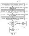
- FIG. 4 is a flow diagram illustrating an embodiment of a process 100 whereby the processing circuitry 24 of the electronic device 10 may execute an authenticity check routine to verify the authenticity of an application 28 contained with a package 27.
- the authenticity check routine may include instructions stored in the memory circuitry 27 for execution by the processing circuitry 24, or instructions stored and executed by a portion of the processing circuitry 24 (e.g., a FPGA) to validate the application 28.
- the illustrated process 100 begins with the processing circuitry 24 determining (block 102) a decryption key stored in the memory circuitry 26 of the electronic device 10. As mentioned above with respect to FIG.
- the package 27 may be partially or entirely encrypted using an encryption key associated with the manufacturer of the electronic device 10 or an authorized software supplier.
- a corresponding key e.g., a decryption key
- the processing circuitry 24 e.g., within a FPGA
- only the digest value 30 may be encrypted, while the remainder of the package 27 stored in the memory circuitry 26 may be unencrypted.
- the processing circuitry 24 of the electronic device 10 may then decrypt (block 104) the encrypted portion of the package 27 using the decryption key determined in block 102.
- the processing circuitry 24 may decrypt the digest value 30, the application 28, or both, as appropriate, using the decryption key.
- the processing circuitry 24 may utilize the HSM 25 or a hardware accelerator to perform one or more functions during the decryption process to improve security, efficiency, or both. Regardless, the processing circuitry 24 may then determine (block 106) the digest value 30 from the decrypted portion of the package 27.
- blocks 102 and 104 may be skipped and the digest value 30 may be directly read from the package 27 without further processing.
- encrypting the entire package 27 may provide greater security to the contents, it may be noted that a greater amount of processing power and time may be consumed by the electronic device 10 to successively decrypt the entire package 27, instead of just the digest value 30, with each execution of the process 100.
- the processing circuitry 24 of the electronic device 10 may calculate (block 108) a digest value for the application 30 of the package 27. That is, the processing circuitry 24 of the electronic device 10 may digest the unencrypted application 28, using a cryptographic hash function (e.g., MD4, MD5, SHA-1, SHA-2, SHA-3, SHA-256), in order to determine a digest value.
- a cryptographic hash function e.g., MD4, MD5, SHA-1, SHA-2, SHA-3, SHA-256
- the processing circuitry 24 may utilize the HSM 25 or a hardware accelerator to perform the digestion for enhanced security or efficiency.
- the processing circuitry 24 of the electronic device 10 may compare (block 110) the calculated digest value to the digest value 30 from the decrypted portion of the package 27. If (block 112) the calculated digest value matches the digest value 30 that was determined from the package 27, then the authenticity check routine process 100 returns a successful result (block 114). If, however (block 112) the calculated digest value does not match the digest value 30 from the package 27, then the authenticity check routine process 100 returns an unsuccessful result (block 116).
- portions of the process 100 illustrated in FIG. 4 may be fairly processor intensive.
- blocks 104 and 108 describe actions that may involve the processing circuitry 24 of the electronic device spending considerable amounts of processing time and energy to execute.
- the authenticity check routine illustrated by the process 100 may only execute when the processing circuitry 24 would otherwise be idle.
- the authenticity check routine of the application 28 may prevent the processing circuitry 24 of the electronic device 10 from entering an idle state, a throttled state, or a low-power sleep state. While this may result in the electronic device 10 consuming more power, operating the processing circuitry 24 in this manner make a differential power analysis or an electromagnetic (EM) noise analysis of the electronic device 10 more difficult.
- EM electromagnetic
- the electronic device 10 since the electronic device 10 does not enter an idle state or a low-power sleep state, an unauthorized party attempting to determine when (during operation of the electronic device 10) and where (in the memory circuitry 26 and/or processing circuitry 24) to attack the electronic device 10 based on an analysis of the power consumption of the electronic device 10 would only see generally uniform power consumption over time.
- the processing circuitry 24 since the processing circuitry 24 may be continually active, an unauthorized party attempting to determine when and where to attack the electronic device 10 based on an analysis of the EM noise generated by the electronic device 10 would only see generally uniform EM noise level over time. As such, the unauthorized party is greatly impaired in gaining unauthorized access to the electronic device 10.
- present embodiments provide a mechanism whereby the authenticity of stored application packages may be continually, regularly, or sporadically verified, even during execution of the stored application itself.
- this authenticity check routine may be executed by the processing circuitry of the electronic device during otherwise idle processing time, rendering the electronic device more robust to thwart differential power analysis and/or EM noise analysis techniques. Accordingly, present embodiments enable the regular authenticity verification of an application in a manner that obfuscates the activities of the electronic device from an unauthorized party, resulting in enhanced security during operation of the electronic device.
Landscapes
- Engineering & Computer Science (AREA)
- Theoretical Computer Science (AREA)
- Computer Security & Cryptography (AREA)
- Software Systems (AREA)
- Physics & Mathematics (AREA)
- Computer Hardware Design (AREA)
- General Physics & Mathematics (AREA)
- General Engineering & Computer Science (AREA)
- Business, Economics & Management (AREA)
- Economics (AREA)
- Health & Medical Sciences (AREA)
- Marketing (AREA)
- Strategic Management (AREA)
- General Business, Economics & Management (AREA)
- Signal Processing (AREA)
- Computer Networks & Wireless Communication (AREA)
- General Health & Medical Sciences (AREA)
- Water Supply & Treatment (AREA)
- Microelectronics & Electronic Packaging (AREA)
- Primary Health Care (AREA)
- Human Resources & Organizations (AREA)
- Tourism & Hospitality (AREA)
- Mathematical Physics (AREA)
- Public Health (AREA)
- Accounting & Taxation (AREA)
- Entrepreneurship & Innovation (AREA)
- Development Economics (AREA)
- Finance (AREA)
- Bioethics (AREA)
- Technology Law (AREA)
- Multimedia (AREA)
- Storage Device Security (AREA)
- Stored Programmes (AREA)
Description
- The subject matter disclosed herein relates to electronic processing devices, and, more specifically to verifying the authenticity of instructions being executed by a processor of an electronic device.
- Certain modem electronic devices, such as cellular phones, digital video recorders, console gaming systems, and so forth, generally include processing circuitry that executes instructions stored in memory in order for the electronic device to function as intended. For example, certain electronic devices may store and execute firmware instructions that generally define the behavior of the electronic device. In certain situations, these firmware instructions may be stored in the memory of the electronic device at the time the electronic device is manufactured. Additionally, in certain situations, the firmware may be updated over the lifetime of the electronic device to address firmware bugs and/or to augment functionality of the electronic device.
- Certain embodiments commensurate in scope with the originally claimed invention are summarized below. These embodiments are not intended to limit the scope of the claimed invention, but rather these embodiments are intended only to provide a brief summary of possible forms of the invention. Indeed, the invention may encompass a variety of forms that may be similar to or different from the embodiments set forth below.
- In an embodiment, a system includes an electronic device having memory circuitry configured to store an application comprising a plurality of instructions. The system also includes processing circuitry configured to execute the application and an application authenticity check routine, wherein the application authenticity check routine includes instructions executable by the processing circuitry to use idle processing time to verify an authenticity of the application throughout execution of the application.
- In another embodiment, a method includes instructing processing circuitry of an electronic device to initiate execution of an application stored in a memory of the electronic device. The method includes executing the application while executing an authenticity check routine using the processor of the electronic device, wherein the authenticity check routine comprises a plurality of instructions configured to cause the processing circuitry to determine whether the application has been modified subsequent to packaging.
- In another embodiment, a non-transitory, computer-readable medium stores instructions executable by at least one processor of an electronic device. The instructions include instructions to execute an application stored in at least one memory of the electronic device and instructions to intermittently execute an authenticity check routine while executing the application. The authenticity check routine includes instructions to compute a digest value for the application stored in the at least one memory of the electronic device and instructions to decrypt a portion of the application stored in the at least one memory of the electronic device to determine a stored digest value for the application. The instructions also include instructions to determine that the application is authentic whenever the at least one processor determines that the computed digest value is equal to the stored digest value.
- These and other features, aspects, and advantages of the present invention will become better understood when the following detailed description is read with reference to the accompanying drawings in which like characters represent like parts throughout the drawings, wherein:
-
FIG. 1 is a schematic of an electronic device, in accordance with an embodiment of the present approach; -
FIG. 2 is a flow diagram illustrating an embodiment of a process for preparing and packaging instructions for execution by the electronic device ofFIG. 1 ; -
FIG. 3 is a flow diagram illustrating an embodiment of a boot process for the electronic device ofFIG. 1 ; and -
FIG. 4 is a flow diagram illustrating an embodiment of an application authenticity check routine. - One or more specific embodiments of the present invention will be described below. In an effort to provide a concise description of these embodiments, all features of an actual implementation may not be described in the specification. It should be appreciated that in the development of any such actual implementation, as in any engineering or design project, numerous implementation-specific decisions must be made to achieve the developers' specific goals, such as compliance with system-related and business-related constraints, which may vary from one implementation to another. Moreover, it should be appreciated that such a development effort might be complex and time consuming, but would nevertheless be a routine undertaking of design, fabrication, and manufacture for those of ordinary skill having the benefit of this disclosure.
- When introducing elements of various embodiments of the present invention, the articles "a," "an," "the," and "said" are intended to mean that there are one or more of the elements. The terms "comprising," "including," and "having" are intended to be inclusive and mean that there may be additional elements other than the listed elements.
- As mentioned above, many modem electronic devices store or encode a set of instructions (e.g., applications, modules, routines, firmware, or any other suitable instructions) that are executed by processing circuitry to enable the electronic device to provide its intended functionality. Additionally, in certain areas, electronic devices may operate for extended periods of time without interruption (e.g., without power cycling or rebooting) after installation and/or activation. For example, an industrial monitoring and/or control system may generally include a number of field devices (e.g., sensing devices, relays, actuators, and so forth), which may be deployed throughout a facility and may subsequently operate for an extended period of time (e.g., months to years) after deployment without interruption. As mentioned, these field devices may generally operate by executing instructions, such as executable applications that are stored in a memory circuitry of the device prior to deployment. In general, if the instructions stored within the memory circuitry of an electronic device are modified, the behavior and functionality of the device will also be modified.
- With the foregoing in mind, present embodiments enable an electronic device to perform an initial check that verifies the authenticity of stored instructions (e.g., firmware) before execution, such as during a booting sequence. As used herein, a set of instructions is considered "authentic" if the instructions have not been modified after packaging (e.g., assembling, bundling) by the manufacturer or another authorized software provider. As set forth above, since certain electronic devices may not be rebooted for extended periods of time, present embodiments also provide a mechanism whereby the authenticity of the stored application packages may be continually, regularly, or sporadically verified during execution of the stored applications. That is, as set forth below, in certain embodiments, the instructions in an executable application may include an authenticity check routine that is continually, regularly, or sporadically executed by the processing circuitry of the electronic device to determine whether the application has been modified subsequent to packaging. In certain embodiments, the authenticity check routine may be executed by the processing circuitry of the electronic device during otherwise idle processing time, rendering the electronic device more robust to thwart differential power analysis and/or electromagnetic (EM) noise analysis techniques. In certain embodiments, the authenticity check routine may be performed using specialized processing circuitry, such as a high-security module (HSM) or a field-programmable gate array (FPGA) (e.g., a hardware accelerator). Accordingly, present embodiments enable the continual, regular, or sporadic authenticity verification of an application, even as it is actively being executed by the electronic device.
- Turning to the drawings,
FIG. 1 is a schematic of anelectronic device 10, in accordance with an embodiment of the present approach. In certain embodiments, theelectronic device 10 may be a consumer device (e.g., a cellular telephone, a tablet computing device, a portable computing device, a desktop computing device, a digital video recorder, a video game console device, a television) or an industrial device (e.g., a relay, an intelligent electronic device (IED), a field device, an end device). In particular, theelectronic device 10 illustrated inFIG. 1 is an embodiment of an intelligent electronic device (IED) 10 that is part of an industrial monitoring and/orcontrol system 12. In addition to theelectronic device 10, the embodiment of the industrial control and/ormonitoring system 12 ofFIG. 1 includes acontroller 14 that monitors and/or controls the operation of the industrial control and/ormonitoring system 12, including theelectronic device 10 and variousindustrial equipment 22. By way of example, theindustrial equipment 22 may include apower distribution system 40 having various power distribution components 41 (e.g., transformers, transmission lines, capacitor banks, etc.), apower generation system 42 having various power generation components 43 (e.g., generators, combustors, engines, etc.), an industrial automation system 44 with various automation components 45 (e.g., reactors, conveyor belts, feeders, hoppers, etc.), awater treatment system 46 having various water treatment components 47 (e.g., filters, clarifiers, pH gauges, etc.), and/or aturbomachinery system 48 having various turbomachine components (e.g., turbines, combustors, compressors, etc.). The illustratedcontroller 14 generally includesprocessing circuitry 16,memory circuitry 18, andcommunication circuitry 20 to enable thecontroller 14 to manage the industrial monitoring and/orcontrol system 12. It may be appreciated that the illustratedindustrial equipment 22 are merely provided as examples of pieces of equipment that may be monitored and/or controlled by theelectronic device 10 and thecontroller 14 of the industrial control and/ormonitoring system 12, and that any other suitable piece of equipment (e.g., a combustor, a blower, a reactor, etc.) may be monitored and/or controlled by the industrial control and/ormonitoring system 12 in accordance with the present disclosure. - The illustrated
electronic device 10 includes processing circuitry 24 (e.g., a general purpose microprocessor, an application-specific integrated circuit (ASIC), or other suitable processing circuitry) that is capable of executing instructions (e.g., executable applications, modules, routines, firmware, and so forth) to provide the desired functionality and behavior of theelectronic device 10. In certain embodiments, thisprocessing circuitry 24 may include a high-security module (HSM) 25, discussed in greater detail below, which may enable enhanced security during certain processing activities. In certain embodiments, thisprocessing circuitry 24 may include a field-programmable gate array (FPGA) device, such as a hardware accelerator, that may be programmed when the device is manufactured to perform certain processing tasks during operation of theelectronic device 10. For such embodiments, the FPGA may be configured or programmed at a hardware-level at the time that theelectronic device 10 is manufactured based on instructions (e.g., software code), such that the FPGA performs the functions described by the instructions during operation. Accordingly, for such embodiments, since the instructions are used to program the FPGA, and since these instructions are carried out by the FPGA during operation, the FPGA may be described herein as storing and executing instructions. - The illustrated
electronic device 10 includes memory circuitry 26 (e.g., electrically erasable programmable read-only memory (EEPROM), a solid state disk drive, a flash drive, or another suitable non-volatile data storage mechanism) capable of storing the aforementioned instructions for execution by theprocessing circuitry 24. For example, as illustrated inFIG. 1 , thememory circuitry 26 stores a package 27 (e.g., software package 27) that, as discussed in greater detail below, includes an executable application 28 (e.g., software 28) as well as adigest value 30 associated with theexecutable application 28. As used herein, an application is a set of encoded instructions (e.g., binary encoded instructions) that are executable by theprocessing circuitry 24 of theelectronic device 10. - The illustrated
electronic device 10 includes input/output (I/O)circuitry 32 capable of receiving user input via one or more input devices (e.g., touchscreens, pointing devices, keyboards, microphones, accelerometers, and so forth) and/or providing output to the user via one or more output devices (e.g., displays, touchscreens, speakers, indicator lights, printers, and so forth). The illustratedelectronic device 10 includes communication circuitry 34 (e.g., a wired or wireless network interface card (NIC)) to enable theelectronic device 10 to communicate with other electronic devices (e.g., the controller 14) via a network (e.g., via a local network or via the internet). The components included in the illustratedelectronic device 10 are merely provided as examples, and that other embodiments of theelectronic device 10 may include additional or fewer components, in accordance with the present disclosure. - Additionally, the illustrated
electronic device 10 includessensor circuitry 36 that enables theelectronic device 10 to collect sensory information regarding the performance of theindustrial equipment 22. In certain embodiments, thesensor circuitry 36 may include, for example, temperature sensors, pressure sensors, flow sensors, composition sensors (e.g., gas composition sensors, oxygen sensors, exhaust gas sensors, etc.), flame sensors, positional sensors, clearance sensors, vibration sensors, accelerometers, rotational speed sensors, voltage sensors, amperage sensors, frequency sensors, light sensors, sound sensors, or any other suitable sensing elements. By specific example, for the illustratedelectronic device 10, thesensor circuitry 36 may include a rotational speed sensor that may be capable of measuring the speed of the turbomachinery 49 (e.g., a drive system of a compressor, a gas turbine, or a steam turbine). That is, theprocessing circuitry 24 may execute a routine of theapplication 28 stored in thememory circuitry 26 of theelectronic device 10 to determine the speed of theturbomachinery 49 based on measurements collected by thesensor circuitry 36. Further, theelectronic device 10 may provide the determined speed of theturbomachinery 49 to thecontroller 14, via thecommunication circuitry 34, such that theprocessor 16 of thecontroller 14 may determine the operation parameters or state of theturbomachinery 49, as well as other portions of the industrial control and/ormonitoring system 12. - The illustrated
electronic device 10 also includescontrol circuitry 38 that enables theelectronic device 10 provide control signals to theturbomachinery 49 to modulate the performance of theturbomachinery 49 based on instructions from thecontroller 14. For example, in certain embodiments, thecontrol circuitry 38 may provide output signals that result in either an increase or a decrease in power being supplied to a drive system of a compressor of theturbomachinery system 48, modulating the performance of the compressor. More specifically, if thecontroller 14 determines that the output of the compressor is too low based on measurements collected by thesensor circuitry 36, then thecontroller 14 may, via thecommunication circuitry 34, instruct theelectronic device 10 to increase the output of the compressor. In response, theelectronic device 10, using thecontrol circuitry 38, may provide control signals to the drive system of the compressor to increase the power supplied to the drive system, thereby increasing the output of the compressor. - As set forth above and discussed in greater detail below, in certain embodiments, the
executable applications 28 may be stored in thememory circuitry 16 at the time theelectronic device 10 is manufactured and may be updated thereafter to address errors or bugs in theinstructions 14 and/or to augment functionality of theelectronic device 10. However, there are some situations that may result in the modification of theexecutable application 28 in thememory circuitry 26 of theelectronic device 10. One possibility is simple data corruption, wherein a hardware glitch, a cosmic ray collision, or another similar event results in a change (e.g., a single bit swap) in theexecutable application 28 stored in thememory circuitry 26. Another possibility is that an unauthorized party may intentionally try to alter one or more bits of data in theexecutable application 28 in an attempt to cause an exception (e.g., a fault) in theelectronic device 10, or in an attempt to gain unauthorized access to theelectronic device 10. If the unauthorized party can gain physical access to theelectronic device 10, this data alteration might be accomplished, for example, by polishing down the integrated circuit (IC) packaging of thememory circuitry 26, and then providing electromagnetic radiation (e.g., laser light) to specific physical locations to alter one or more bits stored in thememory circuitry 26. It should be noted that this example is not intended to be limiting, and that other types of attacks generally involving the application of different types electromagnetic radiation to thememory circuitry 26 and/or theprocessing circuitry 24 may also be possible. - As such, in light of such attacks, present embodiments provide a mechanism to verify the authenticity of the
application 28 throughout execution of theapplication 28. That is, rather than only verifying the authenticity of an application before it is executed (e.g., during bootup), present embodiments are able to identify and address even single bit changes to the contents of theapplication 28 that may occur at any point during the execution of theapplication 28. Further, it may be noted that the success of the EM attack described above is greater when the unauthorized party can ascertain where (in thememory circuitry 26 and/or the processing circuitry 24) or when (during operation of the electronic device 10) to attack the circuitry of theelectronic device 10. As such, certain presently disclosed embodiments enable theprocessing circuitry 24 of theelectronic device 10 to continually be active, continually verifying the authenticity of theapplication 28, which makes it more difficult for an unauthorized party to plan and implement an attack, rendering theelectronic device 10 more secure. -
FIG. 2 is a flow diagram that depicts an embodiment of a computer-implementedprocess 50 whereby an authorized software provider, such as the manufacturer of theelectronic device 10, may generate a package 27 (e.g., a software package 27) for installation in thememory circuitry 26 of theelectronic device 10. The illustratedprocess 50 begins with the authorized software provider compiling (block 52) instructions to generate anexecutable application 28. For example, using a suitable processing device, a set of human-readable code written in a programming language (e.g., C, C++, Ada, Fortran) may be compiled into a binaryexecutable application 28. - Continuing through the
process 50 illustrated inFIG. 2 , next a digest value may be calculated (block 54) for the application compiled inblock 52. That is, using a suitable processing device, theexecutable application 28 generated inblock 52 may be provided as input to an algorithm that outputs a digestvalue 30. The digestvalue 30 may generally be a cryptographic hash value that is computed (e.g., generated or determined) using a cryptographic hash function (e.g., MD4, MD5, SHA-1, SHA-2, SHA-3, SHA-256). As such, the digestvalue 30 may generally include a fixed-length string that is generated from a bit-wise digestion of theapplication 28, such that even a single bit difference in the input (e.g., the application 28) yields different digestvalue 30. - Subsequently, using a suitable processing device, a package 27 (e.g., a software package 27) may be generated (block 56) that includes the
application 30 generated inblock 52 as well as the digestvalue 30 generated inblock 54. For example, thepackage 27 may be a file container (e.g., a zip file, a tar file) that includes a binaryexecutable application file 30 and a text file that includes the digestvalue 30. In certain embodiments, thepackage 27 may be compressed such that thepackage 27 occupies less space in thememory circuitry 26 of theelectronic device 10. Further, in certain embodiments, thepackage 27 may be entirely or partially encrypted. That is, in certain embodiments, a suitable processing device may use an encryption key that is associated with the manufacturer of theelectronic device 10, or an encryption key associated with an authorized software provider, to encrypt some or all of thepackage 27. For example, in certain embodiments, theentire package 27 may be encrypted. In other embodiments, theapplication 28 and the digestvalue 30 stored within thepackage 27 may be individually encrypted. In still other embodiments, the digestvalue 30 alone may be encrypted before being included in thepackage 27. Further, as discussed below, for embodiments that utilize encryption, the encryption key used by the manufacturer or the authorized software provider to encrypt thepackage 27 are associated with corresponding decryption keys stored within thememory circuitry 26 of theelectronic device 10, for example, at the time of manufacturing. - With the foregoing in mind,
FIG. 3 is a flow diagram illustrating an embodiment of aprocess 60 in which theelectronic device 10 boots, verifies, and conditionally executes an application. The illustratedprocess 60 begins as theelectronic device 10 is powered on (block 62). After powering on, theelectronic device 10 may, in certain embodiments, perform one or more checks (e.g., a memory check of thememory circuitry 26, a voltage check of the processing circuitry 24) to verify the proper operation of the hardware components of the electronic device before proceeding. Next, theprocessing circuitry 24 of theelectronic device 10 may begin executing a bootloader application (block 64). The bootloader application may be a collection of instructions stored in thememory circuitry 26 and executable by theprocessing circuitry 24 of theelectronic device 10 that enable an application to be selected, verified, and conditionally executed. - The
processing circuitry 24 of theelectronic device 10 executing the bootloader application may then determine (block 66) an application, stored in thememory circuitry 26, to be executed. For example, in certain embodiments, the bootloader application may prompt a user (e.g., using the I/O circuitry 32 discussed above) to select aparticular application 28 stored in thememory circuitry 26 for execution. In other embodiments, the bootloader application may automatically select anapplication 28 to execute based on identifying information associated with the application 28 (e.g., name, size, version, or location in the memory circuitry 26). - Next, the illustrated
process 60 continues as theprocessing circuitry 24 of theelectronic device 10 executes (block 68) an integrity check routine on thepackage 27, which includes theapplication 28. In certain embodiments, the integrity check routine may be part of the bootloader application, or may be a separate routine called by the bootloader application. As used herein, an integrity check is a high-level check that generally ensures that thepackage 27 likely includes a legitimate application, but does not involve a bit-wise analysis of the contents of thepackage 27 or theapplication 28. For example, the integrity check may ensure that thepackage 27 is the appropriate file type (e.g., a zip file, or a tar file), that thepackage 27 includes a binaryexecutable file 28 and a digestvalue 30, that thepackage 27 is the correct file size, that thepackage 27 conforms to the proper file naming standards, or other high-level checks. In certain embodiments, the integrity check routine may involve the computation and comparison of a checksum value (e.g., a cyclic redundancy check (CRC)) to verify the integrity of thepackage 27, as well as theapplication 28 stored therein. - If (block 70) the
package 27 does not pass the integrity check, theprocessing circuitry 24 of the electronic device may modify (block 72) theapplication 28 and/or theapplication package 27 to render it non-bootable. For example, if the integrity check routine of a bootloader application determines that thepackage 27 or theapplication 28 lacks integrity, then the bootloader application may modify the contents of thepackage 27 and/or the application 28 (e.g., insert a flag, modify the value of one or more bits, or erase thepackage 27 altogether) such that the bootloader will not attempt to execute theapplication 28 again. Subsequently, the bootloader causes theelectronic device 10 to perform a system reset (block 74), enabling the electronic device to begin executing the bootloader application anew (block 64). - If, however (block 70), the
package 27 does pass the integrity check, theprocessing circuitry 24 may then execute (block 76) an authenticity check routine on thepackage 27, which includes theapplication 28. An example of an authenticity check routine is discussed in detail below with respect toFIG. 4 . In certain embodiments, the authenticity check routine ofblock 76 may be part of the bootloader application, or may be a separate routine called by the bootloader application. Regardless, as set forth below, the authenticity check routine generally performs a bit-wise analysis of theapplication 28 stored in thepackage 27 to determine if theapplication 28 matches the digestvalue 30 also stored in thepackage 27. As with the integrity check discussed above, if (block 78) theprocessing circuitry 24 of theelectronic device 10 determines that theapplication 28 of thepackage 27 is not authentic, then theprocessing circuitry 24 may modify (block 72) thepackage 27 and/or theapplication 28 to render it un-bootable and initiate a system reset (block 74). In certain embodiments, the modification (block 72) of the application may be skipped when an application fails an integrity or authenticity check (e.g., blocks 70, 78, or 88), and the device may instead proceed directly to the system reset (block 74), which effectively prevents the device from executing the application in question without the modification ofblock 72. - If, however (block 80) the
package 27 does pass the authenticity check, then theprocessing circuitry 24 may begin executing the application 28 (block 80). As illustrated inFIG. 3 , during execution, theapplication 28 spawns an initial thread or process 82 (e.g., thread or process 0) in addition to other threads or processes 84 and 86. Additionally, in executing theinitial thread 82 of theapplication 28, theprocessing circuitry 24 of theelectronic device 10 may execute (block 88) an authenticity routine to again verify the authenticity of thepackage 27 and theapplication 28. In other words, in certain embodiments, theapplication 28 includes an authenticity check routine that instructs theprocessing circuitry 24 of theelectronic device 10 to verify the authenticity of theapplication 28 currently being executed. An example of an authenticity check routine is discussed in detail below with respect toFIG. 4 . In certain embodiments, theprocessing circuitry 24 may include multiple processing units (e.g., processing cores), and a particular processing unit may be used or dedicated to the execution of the authenticity check routine ofblocks 76 and/or 88. In certain embodiments, theprocessing circuitry 24 may include a HSM that executes the authenticity check routine. In certain embodiments, the authenticity check routine may be stored separately (e.g., in a separate memory device or a separate memory location) from theapplication 28. For example, in certain embodiments, the authenticity check routine may be performed by a hardware accelerator (e.g., a FPGA) that stores and executes instructions to perform an authenticity check routine of theapplication 28. - As set forth below, the authenticity check routine generally performs a bit-wise analysis of the
application 28 stored in thepackage 27 to determine if theapplication 28 still matches the digestvalue 30 also stored in thepackage 27. As such, the authenticity check routine ofblocks package 27 and theapplication 28 that may unintentionally occur (e.g., due to data corruption) or intentionally occur (e.g., due to an unauthorized access attempt) during execution of theapplication 28. As with the integrity check and the authenticity check performed by the bootloader above, if (block 90) the authenticity check routine determines that theapplication 28 is not authentic, then theprocessing circuitry 24 of theelectronic device 10 may render theapplication 28 un-bootable (block 72) and/or initiate a system reset (block 74). - If, however (block 90), the
processing circuitry 24 of theelectronic device 10 successfully verifies the authenticity of theapplication 28, then theprocessing circuitry 24 may once again execute the authenticity check routine ofblock 88. In certain embodiments, theprocessing circuitry 24 may wait a set amount of time (e.g., between approximately 300 milliseconds and approximately 1 month, between approximately 1 second and approximately 1 week, between approximately 1 minute and approximately 1 day, or between approximately 1 hour and approximately 12 hours) or a random amount of time before re-executing the authenticity check ofblock 88, while in other embodiments, theprocessing circuitry 24 may immediately proceed with executing the authenticity check routine once more. In other embodiments, thethread 82 that includesblock 88 may be continually executed throughout execution of theapplication 28. More specifically, in certain embodiments, thethread 82, which includes the authenticity check routine ofblock 88, may be executed concurrently with theother thread thread thread 82, which includes the authenticity check routine ofblock 88, may be readily preempted by theother threads thread 82 only executes when the other thread are waiting or sleeping. In this manner, thethread 82, including the authenticity check routine ofblock 88, may only execute during time periods when some or all of theprocessing circuitry 24 would otherwise sit idle. -
FIG. 4 is a flow diagram illustrating an embodiment of aprocess 100 whereby theprocessing circuitry 24 of theelectronic device 10 may execute an authenticity check routine to verify the authenticity of anapplication 28 contained with apackage 27. As mentioned above, in certain embodiments, the authenticity check routine may include instructions stored in thememory circuitry 27 for execution by theprocessing circuitry 24, or instructions stored and executed by a portion of the processing circuitry 24 (e.g., a FPGA) to validate theapplication 28. The illustratedprocess 100 begins with theprocessing circuitry 24 determining (block 102) a decryption key stored in thememory circuitry 26 of theelectronic device 10. As mentioned above with respect toFIG. 2 , in certain embodiments, thepackage 27 may be partially or entirely encrypted using an encryption key associated with the manufacturer of theelectronic device 10 or an authorized software supplier. For such embodiments, as mentioned above, during manufacturing of theelectronic device 10, a corresponding key (e.g., a decryption key) may be stored in thememory circuitry 26 or the processing circuitry 24 (e.g., within a FPGA) of theelectronic device 10, which enables theprocessing circuitry 24 to decrypt the encrypted portions of thepackage 27. For example, in certain embodiments, only the digestvalue 30 may be encrypted, while the remainder of thepackage 27 stored in thememory circuitry 26 may be unencrypted. - Accordingly, for embodiments in which the
package 27 is at least partially encrypted, theprocessing circuitry 24 of theelectronic device 10 may then decrypt (block 104) the encrypted portion of thepackage 27 using the decryption key determined inblock 102. For example, theprocessing circuitry 24 may decrypt the digestvalue 30, theapplication 28, or both, as appropriate, using the decryption key. In certain embodiments, theprocessing circuitry 24 may utilize theHSM 25 or a hardware accelerator to perform one or more functions during the decryption process to improve security, efficiency, or both. Regardless, theprocessing circuitry 24 may then determine (block 106) the digestvalue 30 from the decrypted portion of thepackage 27. It may be appreciated that, for embodiments in which thepackage 27 is not encrypted, blocks 102 and 104 may be skipped and the digestvalue 30 may be directly read from thepackage 27 without further processing. However, it may generally be desirable for at least the digestvalue 30 within thepackage 27 to be encrypted to prevent the digestvalue 30 from being easily altered after creation of thepackage 27. Further, while encrypting theentire package 27 may provide greater security to the contents, it may be noted that a greater amount of processing power and time may be consumed by theelectronic device 10 to successively decrypt theentire package 27, instead of just the digestvalue 30, with each execution of theprocess 100. - Next in the illustrated
process 100 ofFIG. 4 , theprocessing circuitry 24 of theelectronic device 10 may calculate (block 108) a digest value for theapplication 30 of thepackage 27. That is, theprocessing circuitry 24 of theelectronic device 10 may digest theunencrypted application 28, using a cryptographic hash function (e.g., MD4, MD5, SHA-1, SHA-2, SHA-3, SHA-256), in order to determine a digest value. In certain embodiments, theprocessing circuitry 24 may utilize theHSM 25 or a hardware accelerator to perform the digestion for enhanced security or efficiency. Once theprocessing circuitry 24 has generated a calculated digest value, as described inblock 108, theprocessing circuitry 24 of theelectronic device 10 may compare (block 110) the calculated digest value to the digestvalue 30 from the decrypted portion of thepackage 27. If (block 112) the calculated digest value matches the digestvalue 30 that was determined from thepackage 27, then the authenticitycheck routine process 100 returns a successful result (block 114). If, however (block 112) the calculated digest value does not match the digestvalue 30 from thepackage 27, then the authenticitycheck routine process 100 returns an unsuccessful result (block 116). - It may be noted that portions of the
process 100 illustrated inFIG. 4 may be fairly processor intensive. For example, blocks 104 and 108 describe actions that may involve theprocessing circuitry 24 of the electronic device spending considerable amounts of processing time and energy to execute. As set forth above, in certain embodiments, the authenticity check routine illustrated by theprocess 100 may only execute when theprocessing circuitry 24 would otherwise be idle. In other words, in certain embodiments, the authenticity check routine of theapplication 28 may prevent theprocessing circuitry 24 of theelectronic device 10 from entering an idle state, a throttled state, or a low-power sleep state. While this may result in theelectronic device 10 consuming more power, operating theprocessing circuitry 24 in this manner make a differential power analysis or an electromagnetic (EM) noise analysis of theelectronic device 10 more difficult. That is, in certain embodiments, since theelectronic device 10 does not enter an idle state or a low-power sleep state, an unauthorized party attempting to determine when (during operation of the electronic device 10) and where (in thememory circuitry 26 and/or processing circuitry 24) to attack theelectronic device 10 based on an analysis of the power consumption of theelectronic device 10 would only see generally uniform power consumption over time. Similarly, in certain embodiments, since theprocessing circuitry 24 may be continually active, an unauthorized party attempting to determine when and where to attack theelectronic device 10 based on an analysis of the EM noise generated by theelectronic device 10 would only see generally uniform EM noise level over time. As such, the unauthorized party is greatly impaired in gaining unauthorized access to theelectronic device 10. - Technical effects of the invention include enabling an electronic device to verify that stored instructions have not been modified after the instructions are packaged or during execution of the instructions. That is, present embodiments provide a mechanism whereby the authenticity of stored application packages may be continually, regularly, or sporadically verified, even during execution of the stored application itself. In certain embodiments, this authenticity check routine may be executed by the processing circuitry of the electronic device during otherwise idle processing time, rendering the electronic device more robust to thwart differential power analysis and/or EM noise analysis techniques. Accordingly, present embodiments enable the regular authenticity verification of an application in a manner that obfuscates the activities of the electronic device from an unauthorized party, resulting in enhanced security during operation of the electronic device.
- This written description uses examples to disclose the invention, including the best mode, and also to enable any person skilled in the art to practice the invention, including making and using any devices or systems and performing any incorporated methods. The patentable scope of the invention is defined by the claims, and may include other examples that occur to those skilled in the art. Such other examples are intended to be within the scope of the claims if they have structural elements that do not differ from the literal language of the claims, or if they include equivalent structural elements with insubstantial differences from the literal language of the claims.
Claims (15)
- A system, comprising:an electronic device (10), comprising:memory circuitry (26) configured to store an application (28) comprising a plurality of instructions; andprocessing circuitry (24) configured to execute the application (28) and an application authenticity check routine, wherein the application authenticity check routine includes instructions executable by the processing circuitry (24) to use idle processing time to verify an authenticity of the application (28) throughout execution of the application (28).
- The system of claim 1, wherein the application authenticity check routine comprises instructions executable by the processing circuitry (24) to determine that the application is authentic when a calculated digest value (30) for the application matches a digest value stored in the application (28).
- The system of claim 2, wherein the application authenticity check routine comprises instructions executable by the processing circuitry (24) to alter the application (28) to render the application non-executable by the processing circuitry (24) and to restart the electronic device (10) when the processing circuitry (24) determines that the calculated digest value for the application does not match the digest value (30) stored in the application (28).
- The system of any of claims 1 to 3, wherein the processing circuitry (24) comprises a high-security module (HSM) (25), and wherein the HSM (25) is configured to execute the application authenticity check routine to verify the authenticity of the application (28) being executed by other portions of the processing circuitry (24).
- The system of any of claims 1 to 4, wherein the processing circuitry (24) includes a field-programmable gate array (FPGA) that is configured to store and execute the application authenticity check routine to verify the authenticity of the application (28) being executed by other portions of the processing circuitry (24).
- The system of any of claims 1 to 5, wherein the application authenticity check routine is configured to make an energy consumption and an electromagnetic (EM) noise level of the electronic device (10) substantially uniform throughout execution of the application (28).
- The system of any preceding claim, wherein the application authenticity check routine is stored in the memory circuitry (26).
- The system of any preceding claim, wherein the electronic device (10) comprises a relay of an industrial monitoring and/or control system, and wherein the industrial monitoring and/or control system (12) comprises a power grid system, a protection and control system, an industrial plant, a power distribution system (40), or any combination thereof.
- A method, comprising:instructing processing circuitry (24) of an electronic device (10) to initiate execution of an application (28) stored in a memory (26) of the electronic device (10); andexecuting the application (28) while executing an authenticity check routine using the processing circuitry (24) of the electronic device (10), wherein the authenticity check routine comprises a plurality of instructions configured to cause the processing circuitry (24) to determine whether the application (28) has been modified subsequent to packaging.
- The method of claim 9, comprising modifying the application (28) in the memory of the electronic device (10) to render the application (28) non-executable when the processing circuitry (24) etermines that the application (28) has been modified subsequent to packaging.
- The method of claim 10, comprising restarting the electronic device (10) after modifying the application (28) when the processing circuitry (24) determines that the application (28) has been modified subsequent to packaging.
- The method of claim 10 or 11, wherein executing the authenticity check routine comprises executing the authenticity check routine using available processing cycles of the processing circuitry (24) of the electronic device (10) while the processing circuitry (24) is executing the application (28).
- A non-transitory, computer-readable medium storing instructions executable by at least one processor (24) of an electronic device (10), the instructions comprising:instructions to execute an application (28) stored in at least one memory (26) of the electronic device (10);instructions to intermittently execute an authenticity check routine while executing the application (28), wherein the authenticity check routine comprises:instructions to compute a digest value for the application stored in the at least one memory (26) of the electronic device (10);instructions to decrypt a portion of the application (28) stored in the at least one memory (26) of the electronic device (10) to determine a stored digest value (30) for the application (28); andinstructions to determine that the application (28) is authentic whenever the at least one processor (24) determines that the computed digest value is equal to the stored digest value (30).
- The medium of claim 13, wherein the authenticity check routine comprises instructions to restart the electronic device (10) whenever the computed digest value is not equal to the stored digest value (30).
- The medium of claim 13 or 14, wherein intermittently executing the application authenticity check routine comprises executing the application authenticity check routine instead of allowing the at least one processor (24) to sit idle or to be throttled, enabling the at least one processor (24) to consume a substantially constant amount of power, enabling the at least one processor (24) to emit a substantially constant amount of electromagnetic radiation, or a combination thereof, while executing the application (28).
Applications Claiming Priority (1)
| Application Number | Priority Date | Filing Date | Title |
|---|---|---|---|
| US14/333,198 US9390258B2 (en) | 2014-07-16 | 2014-07-16 | Systems and methods for verifying the authenticity of an application during execution |
Publications (2)
| Publication Number | Publication Date |
|---|---|
| EP2975546A1 true EP2975546A1 (en) | 2016-01-20 |
| EP2975546B1 EP2975546B1 (en) | 2018-06-13 |
Family
ID=53716309
Family Applications (1)
| Application Number | Title | Priority Date | Filing Date |
|---|---|---|---|
| EP15175920.6A Not-in-force EP2975546B1 (en) | 2014-07-16 | 2015-07-08 | Systems and methods for verifying the authenticity of an application during execution |
Country Status (6)
| Country | Link |
|---|---|
| US (1) | US9390258B2 (en) |
| EP (1) | EP2975546B1 (en) |
| JP (1) | JP2016024821A (en) |
| CN (1) | CN105279428A (en) |
| BR (1) | BR102015016943A2 (en) |
| CA (1) | CA2896775A1 (en) |
Cited By (1)
| Publication number | Priority date | Publication date | Assignee | Title |
|---|---|---|---|---|
| CN109412884A (en) * | 2018-08-21 | 2019-03-01 | 平安科技(深圳)有限公司 | Performance data acquisition method, device and storage medium, the server of component |
Families Citing this family (5)
| Publication number | Priority date | Publication date | Assignee | Title |
|---|---|---|---|---|
| US10645073B1 (en) * | 2017-06-12 | 2020-05-05 | Ca, Inc. | Systems and methods for authenticating applications installed on computing devices |
| EP3667529B1 (en) | 2018-12-14 | 2024-02-28 | Siemens Aktiengesellschaft | Method and device for authenticating an fpga configuration |
| KR102793219B1 (en) * | 2019-01-17 | 2025-04-07 | 주식회사 엘지에너지솔루션 | Memory, error restoration method of the memory, and battery device comprising the memory |
| JP7249968B2 (en) * | 2020-03-09 | 2023-03-31 | 株式会社東芝 | Information processing equipment and storage |
| US12596572B2 (en) * | 2023-03-21 | 2026-04-07 | DSP Concepts, Inc. | Audio multithreaded profiling |
Citations (2)
| Publication number | Priority date | Publication date | Assignee | Title |
|---|---|---|---|---|
| EP1273993A2 (en) * | 2001-07-02 | 2003-01-08 | Robert Bosch Gmbh | Method for protecing a microprocessor system against software manipulation |
| WO2004055634A2 (en) * | 2002-12-12 | 2004-07-01 | Finite State Machine Labs, Inc. | Systems and methods for detecting a security breach in a computer system |
Family Cites Families (19)
| Publication number | Priority date | Publication date | Assignee | Title |
|---|---|---|---|---|
| US6138236A (en) | 1996-07-01 | 2000-10-24 | Sun Microsystems, Inc. | Method and apparatus for firmware authentication |
| EP1333350A1 (en) * | 2002-01-30 | 2003-08-06 | STMicroelectronics Limited | Memory security device |
| US8393001B1 (en) | 2002-07-26 | 2013-03-05 | Mcafee, Inc. | Secure signature server system and associated method |
| EP1429224A1 (en) | 2002-12-10 | 2004-06-16 | Texas Instruments Incorporated | Firmware run-time authentication |
| US7401234B2 (en) * | 2004-03-01 | 2008-07-15 | Freescale Semiconductor, Inc. | Autonomous memory checker for runtime security assurance and method therefore |
| JP2007226277A (en) * | 2004-04-02 | 2007-09-06 | Matsushita Electric Ind Co Ltd | Virtual machine alteration inspection method and virtual machine alteration inspection device |
| WO2006082994A2 (en) * | 2005-02-07 | 2006-08-10 | Sony Computer Entertainment Inc. | Methods and apparatus for facilitating a secure session between a processor and an external device |
| US8051299B2 (en) * | 2006-03-20 | 2011-11-01 | Hewlett-Packard Development Company, L.P. | Computer security method and computer system |
| US8060941B2 (en) * | 2006-12-15 | 2011-11-15 | International Business Machines Corporation | Method and system to authenticate an application in a computing platform operating in trusted computing group (TCG) domain |
| US20090119221A1 (en) * | 2007-11-05 | 2009-05-07 | Timothy Martin Weston | System and Method for Cryptographically Authenticated Display Prompt Control for Multifunctional Payment Terminals |
| US8607216B2 (en) | 2008-08-01 | 2013-12-10 | Palm, Inc. | Verifying firmware |
| US8832454B2 (en) | 2008-12-30 | 2014-09-09 | Intel Corporation | Apparatus and method for runtime integrity verification |
| US9250671B2 (en) * | 2011-02-16 | 2016-02-02 | Honeywell International Inc. | Cryptographic logic circuit with resistance to differential power analysis |
| JP5961638B2 (en) * | 2011-02-17 | 2016-08-02 | ターセーラ, インコーポレイテッド | System and method for application certification |
| WO2013078415A1 (en) * | 2011-11-22 | 2013-05-30 | Iolo Technologies, Llc | Idle detection |
| CN102737192B (en) * | 2012-07-09 | 2015-11-25 | 江南大学 | A kind of trusted program operation file backup method stored based on cloud |
| WO2014036021A1 (en) * | 2012-08-28 | 2014-03-06 | Visa International Service Association | Secure device service enrollment |
| US9129114B2 (en) * | 2012-12-03 | 2015-09-08 | Imation Corp. | Preboot environment with system security check |
| CN103442026B (en) * | 2013-02-05 | 2017-03-08 | 华为技术有限公司 | A kind of applied program processing method, device and system |
-
2014
- 2014-07-16 US US14/333,198 patent/US9390258B2/en not_active Expired - Fee Related
-
2015
- 2015-07-08 EP EP15175920.6A patent/EP2975546B1/en not_active Not-in-force
- 2015-07-09 CA CA2896775A patent/CA2896775A1/en not_active Abandoned
- 2015-07-13 JP JP2015139290A patent/JP2016024821A/en active Pending
- 2015-07-15 BR BR102015016943A patent/BR102015016943A2/en not_active Application Discontinuation
- 2015-07-16 CN CN201510417660.4A patent/CN105279428A/en active Pending
Patent Citations (2)
| Publication number | Priority date | Publication date | Assignee | Title |
|---|---|---|---|---|
| EP1273993A2 (en) * | 2001-07-02 | 2003-01-08 | Robert Bosch Gmbh | Method for protecing a microprocessor system against software manipulation |
| WO2004055634A2 (en) * | 2002-12-12 | 2004-07-01 | Finite State Machine Labs, Inc. | Systems and methods for detecting a security breach in a computer system |
Cited By (1)
| Publication number | Priority date | Publication date | Assignee | Title |
|---|---|---|---|---|
| CN109412884A (en) * | 2018-08-21 | 2019-03-01 | 平安科技(深圳)有限公司 | Performance data acquisition method, device and storage medium, the server of component |
Also Published As
| Publication number | Publication date |
|---|---|
| EP2975546B1 (en) | 2018-06-13 |
| BR102015016943A2 (en) | 2016-01-19 |
| US9390258B2 (en) | 2016-07-12 |
| CN105279428A (en) | 2016-01-27 |
| US20160019383A1 (en) | 2016-01-21 |
| JP2016024821A (en) | 2016-02-08 |
| CA2896775A1 (en) | 2016-01-16 |
Similar Documents
| Publication | Publication Date | Title |
|---|---|---|
| EP2975546B1 (en) | Systems and methods for verifying the authenticity of an application during execution | |
| EP2660668B1 (en) | System and method for controlling file execution for industrial control systems | |
| US8964973B2 (en) | Systems and methods for controlling file execution for industrial control systems | |
| US10417425B2 (en) | Secured cyber-physical systems | |
| CN106775716B (en) | Trusted PLC (programmable logic controller) starting method based on measurement mechanism | |
| JP6373888B2 (en) | Information processing apparatus and control method | |
| US20130191624A1 (en) | Firmware protection and validation | |
| ES2866885T3 (en) | System and procedure for cryptographically protected surveillance of at least one component of a device or installation | |
| JP2008204459A (en) | Hibernation of processing apparatus for processing secure data | |
| Habibi et al. | Mavr: Code reuse stealthy attacks and mitigation on unmanned aerial vehicles | |
| Daniels et al. | S μ v-the security microvisor: a virtualisation-based security middleware for the internet of things | |
| US20220284104A1 (en) | Secure Boot Process for a Computer System | |
| US20200233676A1 (en) | Bios management device, bios management system, bios management method, and bios management program-stored recording medium | |
| CN109753788B (en) | Integrity checking method and computer readable storage medium during kernel operation | |
| KR101988404B1 (en) | Soc having double security features, and double security method for soc | |
| KR101954439B1 (en) | Soc having double security features, and double security method for soc | |
| Caulfield et al. | TRACES: TEE-based runtime auditing for commodity embedded systems | |
| CN109857385A (en) | Application file packaging method, installation method and starting method | |
| Francillon et al. | Systematic treatment of remote attestation | |
| JP2021034011A (en) | Computer system with forced self-authentication | |
| US11947807B2 (en) | Method and device for processing data stored in a memory unit | |
| WO2018194568A1 (en) | Executing processes in sequence | |
| JP2015049785A (en) | Program processing device | |
| EP3046024B1 (en) | Method of operating a system on chip comprising a bootable processor | |
| CN117094035A (en) | PLC software protection method and device |
Legal Events
| Date | Code | Title | Description |
|---|---|---|---|
| PUAI | Public reference made under article 153(3) epc to a published international application that has entered the european phase |
Free format text: ORIGINAL CODE: 0009012 |
|
| AK | Designated contracting states |
Kind code of ref document: A1 Designated state(s): AL AT BE BG CH CY CZ DE DK EE ES FI FR GB GR HR HU IE IS IT LI LT LU LV MC MK MT NL NO PL PT RO RS SE SI SK SM TR |
|
| AX | Request for extension of the european patent |
Extension state: BA ME |
|
| 17P | Request for examination filed |
Effective date: 20160720 |
|
| RBV | Designated contracting states (corrected) |
Designated state(s): AL AT BE BG CH CY CZ DE DK EE ES FI FR GB GR HR HU IE IS IT LI LT LU LV MC MK MT NL NO PL PT RO RS SE SI SK SM TR |
|
| 17Q | First examination report despatched |
Effective date: 20161201 |
|
| GRAP | Despatch of communication of intention to grant a patent |
Free format text: ORIGINAL CODE: EPIDOSNIGR1 |
|
| INTG | Intention to grant announced |
Effective date: 20180302 |
|
| GRAS | Grant fee paid |
Free format text: ORIGINAL CODE: EPIDOSNIGR3 |
|
| GRAA | (expected) grant |
Free format text: ORIGINAL CODE: 0009210 |
|
| AK | Designated contracting states |
Kind code of ref document: B1 Designated state(s): AL AT BE BG CH CY CZ DE DK EE ES FI FR GB GR HR HU IE IS IT LI LT LU LV MC MK MT NL NO PL PT RO RS SE SI SK SM TR |
|
| REG | Reference to a national code |
Ref country code: GB Ref legal event code: FG4D |
|
| REG | Reference to a national code |
Ref country code: CH Ref legal event code: EP Ref country code: AT Ref legal event code: REF Ref document number: 1009206 Country of ref document: AT Kind code of ref document: T Effective date: 20180615 |
|
| REG | Reference to a national code |
Ref country code: IE Ref legal event code: FG4D |
|
| REG | Reference to a national code |
Ref country code: DE Ref legal event code: R096 Ref document number: 602015012142 Country of ref document: DE |
|
| REG | Reference to a national code |
Ref country code: FR Ref legal event code: PLFP Year of fee payment: 4 |
|
| REG | Reference to a national code |
Ref country code: SE Ref legal event code: TRGR |
|
| REG | Reference to a national code |
Ref country code: NL Ref legal event code: MP Effective date: 20180613 |
|
| REG | Reference to a national code |
Ref country code: LT Ref legal event code: MG4D |
|
| PG25 | Lapsed in a contracting state [announced via postgrant information from national office to epo] |
Ref country code: ES Free format text: LAPSE BECAUSE OF FAILURE TO SUBMIT A TRANSLATION OF THE DESCRIPTION OR TO PAY THE FEE WITHIN THE PRESCRIBED TIME-LIMIT Effective date: 20180613 Ref country code: LT Free format text: LAPSE BECAUSE OF FAILURE TO SUBMIT A TRANSLATION OF THE DESCRIPTION OR TO PAY THE FEE WITHIN THE PRESCRIBED TIME-LIMIT Effective date: 20180613 Ref country code: CY Free format text: LAPSE BECAUSE OF FAILURE TO SUBMIT A TRANSLATION OF THE DESCRIPTION OR TO PAY THE FEE WITHIN THE PRESCRIBED TIME-LIMIT Effective date: 20180613 Ref country code: BG Free format text: LAPSE BECAUSE OF FAILURE TO SUBMIT A TRANSLATION OF THE DESCRIPTION OR TO PAY THE FEE WITHIN THE PRESCRIBED TIME-LIMIT Effective date: 20180913 Ref country code: FI Free format text: LAPSE BECAUSE OF FAILURE TO SUBMIT A TRANSLATION OF THE DESCRIPTION OR TO PAY THE FEE WITHIN THE PRESCRIBED TIME-LIMIT Effective date: 20180613 Ref country code: NO Free format text: LAPSE BECAUSE OF FAILURE TO SUBMIT A TRANSLATION OF THE DESCRIPTION OR TO PAY THE FEE WITHIN THE PRESCRIBED TIME-LIMIT Effective date: 20180913 |
|
| PG25 | Lapsed in a contracting state [announced via postgrant information from national office to epo] |
Ref country code: GR Free format text: LAPSE BECAUSE OF FAILURE TO SUBMIT A TRANSLATION OF THE DESCRIPTION OR TO PAY THE FEE WITHIN THE PRESCRIBED TIME-LIMIT Effective date: 20180914 Ref country code: RS Free format text: LAPSE BECAUSE OF FAILURE TO SUBMIT A TRANSLATION OF THE DESCRIPTION OR TO PAY THE FEE WITHIN THE PRESCRIBED TIME-LIMIT Effective date: 20180613 Ref country code: LV Free format text: LAPSE BECAUSE OF FAILURE TO SUBMIT A TRANSLATION OF THE DESCRIPTION OR TO PAY THE FEE WITHIN THE PRESCRIBED TIME-LIMIT Effective date: 20180613 Ref country code: HR Free format text: LAPSE BECAUSE OF FAILURE TO SUBMIT A TRANSLATION OF THE DESCRIPTION OR TO PAY THE FEE WITHIN THE PRESCRIBED TIME-LIMIT Effective date: 20180613 |
|
| REG | Reference to a national code |
Ref country code: AT Ref legal event code: MK05 Ref document number: 1009206 Country of ref document: AT Kind code of ref document: T Effective date: 20180613 |
|
| PG25 | Lapsed in a contracting state [announced via postgrant information from national office to epo] |
Ref country code: NL Free format text: LAPSE BECAUSE OF FAILURE TO SUBMIT A TRANSLATION OF THE DESCRIPTION OR TO PAY THE FEE WITHIN THE PRESCRIBED TIME-LIMIT Effective date: 20180613 |
|
| PG25 | Lapsed in a contracting state [announced via postgrant information from national office to epo] |
Ref country code: CZ Free format text: LAPSE BECAUSE OF FAILURE TO SUBMIT A TRANSLATION OF THE DESCRIPTION OR TO PAY THE FEE WITHIN THE PRESCRIBED TIME-LIMIT Effective date: 20180613 Ref country code: SK Free format text: LAPSE BECAUSE OF FAILURE TO SUBMIT A TRANSLATION OF THE DESCRIPTION OR TO PAY THE FEE WITHIN THE PRESCRIBED TIME-LIMIT Effective date: 20180613 Ref country code: EE Free format text: LAPSE BECAUSE OF FAILURE TO SUBMIT A TRANSLATION OF THE DESCRIPTION OR TO PAY THE FEE WITHIN THE PRESCRIBED TIME-LIMIT Effective date: 20180613 Ref country code: PL Free format text: LAPSE BECAUSE OF FAILURE TO SUBMIT A TRANSLATION OF THE DESCRIPTION OR TO PAY THE FEE WITHIN THE PRESCRIBED TIME-LIMIT Effective date: 20180613 Ref country code: RO Free format text: LAPSE BECAUSE OF FAILURE TO SUBMIT A TRANSLATION OF THE DESCRIPTION OR TO PAY THE FEE WITHIN THE PRESCRIBED TIME-LIMIT Effective date: 20180613 Ref country code: IS Free format text: LAPSE BECAUSE OF FAILURE TO SUBMIT A TRANSLATION OF THE DESCRIPTION OR TO PAY THE FEE WITHIN THE PRESCRIBED TIME-LIMIT Effective date: 20181013 Ref country code: AT Free format text: LAPSE BECAUSE OF FAILURE TO SUBMIT A TRANSLATION OF THE DESCRIPTION OR TO PAY THE FEE WITHIN THE PRESCRIBED TIME-LIMIT Effective date: 20180613 |
|
| PG25 | Lapsed in a contracting state [announced via postgrant information from national office to epo] |
Ref country code: SM Free format text: LAPSE BECAUSE OF FAILURE TO SUBMIT A TRANSLATION OF THE DESCRIPTION OR TO PAY THE FEE WITHIN THE PRESCRIBED TIME-LIMIT Effective date: 20180613 Ref country code: IT Free format text: LAPSE BECAUSE OF FAILURE TO SUBMIT A TRANSLATION OF THE DESCRIPTION OR TO PAY THE FEE WITHIN THE PRESCRIBED TIME-LIMIT Effective date: 20180613 |
|
| REG | Reference to a national code |
Ref country code: CH Ref legal event code: PL |
|
| REG | Reference to a national code |
Ref country code: DE Ref legal event code: R097 Ref document number: 602015012142 Country of ref document: DE |
|
| PG25 | Lapsed in a contracting state [announced via postgrant information from national office to epo] |
Ref country code: MC Free format text: LAPSE BECAUSE OF FAILURE TO SUBMIT A TRANSLATION OF THE DESCRIPTION OR TO PAY THE FEE WITHIN THE PRESCRIBED TIME-LIMIT Effective date: 20180613 Ref country code: LU Free format text: LAPSE BECAUSE OF NON-PAYMENT OF DUE FEES Effective date: 20180708 |
|
| REG | Reference to a national code |
Ref country code: BE Ref legal event code: MM Effective date: 20180731 |
|
| REG | Reference to a national code |
Ref country code: IE Ref legal event code: MM4A |
|
| PLBE | No opposition filed within time limit |
Free format text: ORIGINAL CODE: 0009261 |
|
| STAA | Information on the status of an ep patent application or granted ep patent |
Free format text: STATUS: NO OPPOSITION FILED WITHIN TIME LIMIT |
|
| PG25 | Lapsed in a contracting state [announced via postgrant information from national office to epo] |
Ref country code: CH Free format text: LAPSE BECAUSE OF NON-PAYMENT OF DUE FEES Effective date: 20180731 Ref country code: IE Free format text: LAPSE BECAUSE OF NON-PAYMENT OF DUE FEES Effective date: 20180708 Ref country code: LI Free format text: LAPSE BECAUSE OF NON-PAYMENT OF DUE FEES Effective date: 20180731 |
|
| 26N | No opposition filed |
Effective date: 20190314 |
|
| PG25 | Lapsed in a contracting state [announced via postgrant information from national office to epo] |
Ref country code: BE Free format text: LAPSE BECAUSE OF NON-PAYMENT OF DUE FEES Effective date: 20180731 Ref country code: SI Free format text: LAPSE BECAUSE OF FAILURE TO SUBMIT A TRANSLATION OF THE DESCRIPTION OR TO PAY THE FEE WITHIN THE PRESCRIBED TIME-LIMIT Effective date: 20180613 Ref country code: DK Free format text: LAPSE BECAUSE OF FAILURE TO SUBMIT A TRANSLATION OF THE DESCRIPTION OR TO PAY THE FEE WITHIN THE PRESCRIBED TIME-LIMIT Effective date: 20180613 |
|
| PG25 | Lapsed in a contracting state [announced via postgrant information from national office to epo] |
Ref country code: AL Free format text: LAPSE BECAUSE OF FAILURE TO SUBMIT A TRANSLATION OF THE DESCRIPTION OR TO PAY THE FEE WITHIN THE PRESCRIBED TIME-LIMIT Effective date: 20180613 |
|
| PG25 | Lapsed in a contracting state [announced via postgrant information from national office to epo] |
Ref country code: MT Free format text: LAPSE BECAUSE OF NON-PAYMENT OF DUE FEES Effective date: 20180708 |
|
| PG25 | Lapsed in a contracting state [announced via postgrant information from national office to epo] |
Ref country code: TR Free format text: LAPSE BECAUSE OF FAILURE TO SUBMIT A TRANSLATION OF THE DESCRIPTION OR TO PAY THE FEE WITHIN THE PRESCRIBED TIME-LIMIT Effective date: 20180613 |
|
| PG25 | Lapsed in a contracting state [announced via postgrant information from national office to epo] |
Ref country code: PT Free format text: LAPSE BECAUSE OF FAILURE TO SUBMIT A TRANSLATION OF THE DESCRIPTION OR TO PAY THE FEE WITHIN THE PRESCRIBED TIME-LIMIT Effective date: 20180613 |
|
| PG25 | Lapsed in a contracting state [announced via postgrant information from national office to epo] |
Ref country code: MK Free format text: LAPSE BECAUSE OF NON-PAYMENT OF DUE FEES Effective date: 20180613 Ref country code: HU Free format text: LAPSE BECAUSE OF FAILURE TO SUBMIT A TRANSLATION OF THE DESCRIPTION OR TO PAY THE FEE WITHIN THE PRESCRIBED TIME-LIMIT; INVALID AB INITIO Effective date: 20150708 |
|
| PGFP | Annual fee paid to national office [announced via postgrant information from national office to epo] |
Ref country code: FR Payment date: 20230621 Year of fee payment: 9 |
|
| PGFP | Annual fee paid to national office [announced via postgrant information from national office to epo] |
Ref country code: SE Payment date: 20230622 Year of fee payment: 9 |
|
| PGFP | Annual fee paid to national office [announced via postgrant information from national office to epo] |
Ref country code: GB Payment date: 20230620 Year of fee payment: 9 |
|
| REG | Reference to a national code |
Ref country code: DE Ref legal event code: R081 Ref document number: 602015012142 Country of ref document: DE Owner name: GENERAL ELECTRIC TECHNOLOGY GMBH, CH Free format text: FORMER OWNER: GENERAL ELECTRIC CO., SCHENECTADY, N.Y., US |
|
| PGFP | Annual fee paid to national office [announced via postgrant information from national office to epo] |
Ref country code: DE Payment date: 20230620 Year of fee payment: 9 |
|
| REG | Reference to a national code |
Ref country code: GB Ref legal event code: 732E Free format text: REGISTERED BETWEEN 20240222 AND 20240228 |
|
| REG | Reference to a national code |
Ref country code: DE Ref legal event code: R119 Ref document number: 602015012142 Country of ref document: DE |
|
| REG | Reference to a national code |
Ref country code: SE Ref legal event code: EUG |
|
| GBPC | Gb: european patent ceased through non-payment of renewal fee |
Effective date: 20240708 |
|
| PG25 | Lapsed in a contracting state [announced via postgrant information from national office to epo] |
Ref country code: DE Free format text: LAPSE BECAUSE OF NON-PAYMENT OF DUE FEES Effective date: 20250201 |
|
| PG25 | Lapsed in a contracting state [announced via postgrant information from national office to epo] |
Ref country code: FR Free format text: LAPSE BECAUSE OF NON-PAYMENT OF DUE FEES Effective date: 20240731 |
|
| PG25 | Lapsed in a contracting state [announced via postgrant information from national office to epo] |
Ref country code: GB Free format text: LAPSE BECAUSE OF NON-PAYMENT OF DUE FEES Effective date: 20240708 |
|
| PG25 | Lapsed in a contracting state [announced via postgrant information from national office to epo] |
Ref country code: SE Free format text: LAPSE BECAUSE OF NON-PAYMENT OF DUE FEES Effective date: 20240709 |