EP2973660B1 - Metal induced nanocrystallization of amorphous semiconductor quantum dots - Google Patents
Metal induced nanocrystallization of amorphous semiconductor quantum dots Download PDFInfo
- Publication number
- EP2973660B1 EP2973660B1 EP14762623.8A EP14762623A EP2973660B1 EP 2973660 B1 EP2973660 B1 EP 2973660B1 EP 14762623 A EP14762623 A EP 14762623A EP 2973660 B1 EP2973660 B1 EP 2973660B1
- Authority
- EP
- European Patent Office
- Prior art keywords
- semiconductor particles
- metal catalyst
- vapor
- amorphous semiconductor
- vacuumed
- Prior art date
- Legal status (The legal status is an assumption and is not a legal conclusion. Google has not performed a legal analysis and makes no representation as to the accuracy of the status listed.)
- Active
Links
Images





Classifications
-
- H—ELECTRICITY
- H10—SEMICONDUCTOR DEVICES; ELECTRIC SOLID-STATE DEVICES NOT OTHERWISE PROVIDED FOR
- H10P—GENERIC PROCESSES OR APPARATUS FOR THE MANUFACTURE OR TREATMENT OF DEVICES COVERED BY CLASS H10
- H10P14/00—Formation of materials, e.g. in the shape of layers or pillars
- H10P14/20—Formation of materials, e.g. in the shape of layers or pillars of semiconductor materials
- H10P14/36—Formation of materials, e.g. in the shape of layers or pillars of semiconductor materials characterised by treatments done before the formation of the materials
-
- C—CHEMISTRY; METALLURGY
- C30—CRYSTAL GROWTH
- C30B—SINGLE-CRYSTAL GROWTH; UNIDIRECTIONAL SOLIDIFICATION OF EUTECTIC MATERIAL OR UNIDIRECTIONAL DEMIXING OF EUTECTOID MATERIAL; REFINING BY ZONE-MELTING OF MATERIAL; PRODUCTION OF A HOMOGENEOUS POLYCRYSTALLINE MATERIAL WITH DEFINED STRUCTURE; SINGLE CRYSTALS OR HOMOGENEOUS POLYCRYSTALLINE MATERIAL WITH DEFINED STRUCTURE; AFTER-TREATMENT OF SINGLE CRYSTALS OR A HOMOGENEOUS POLYCRYSTALLINE MATERIAL WITH DEFINED STRUCTURE; APPARATUS THEREFOR
- C30B1/00—Single-crystal growth directly from the solid state
- C30B1/02—Single-crystal growth directly from the solid state by thermal treatment, e.g. strain annealing
- C30B1/023—Single-crystal growth directly from the solid state by thermal treatment, e.g. strain annealing from solids with amorphous structure
-
- C—CHEMISTRY; METALLURGY
- C30—CRYSTAL GROWTH
- C30B—SINGLE-CRYSTAL GROWTH; UNIDIRECTIONAL SOLIDIFICATION OF EUTECTIC MATERIAL OR UNIDIRECTIONAL DEMIXING OF EUTECTOID MATERIAL; REFINING BY ZONE-MELTING OF MATERIAL; PRODUCTION OF A HOMOGENEOUS POLYCRYSTALLINE MATERIAL WITH DEFINED STRUCTURE; SINGLE CRYSTALS OR HOMOGENEOUS POLYCRYSTALLINE MATERIAL WITH DEFINED STRUCTURE; AFTER-TREATMENT OF SINGLE CRYSTALS OR A HOMOGENEOUS POLYCRYSTALLINE MATERIAL WITH DEFINED STRUCTURE; APPARATUS THEREFOR
- C30B28/00—Production of homogeneous polycrystalline material with defined structure
- C30B28/02—Production of homogeneous polycrystalline material with defined structure directly from the solid state
-
- C—CHEMISTRY; METALLURGY
- C30—CRYSTAL GROWTH
- C30B—SINGLE-CRYSTAL GROWTH; UNIDIRECTIONAL SOLIDIFICATION OF EUTECTIC MATERIAL OR UNIDIRECTIONAL DEMIXING OF EUTECTOID MATERIAL; REFINING BY ZONE-MELTING OF MATERIAL; PRODUCTION OF A HOMOGENEOUS POLYCRYSTALLINE MATERIAL WITH DEFINED STRUCTURE; SINGLE CRYSTALS OR HOMOGENEOUS POLYCRYSTALLINE MATERIAL WITH DEFINED STRUCTURE; AFTER-TREATMENT OF SINGLE CRYSTALS OR A HOMOGENEOUS POLYCRYSTALLINE MATERIAL WITH DEFINED STRUCTURE; APPARATUS THEREFOR
- C30B29/00—Single crystals or homogeneous polycrystalline material with defined structure characterised by the material or by their shape
- C30B29/02—Elements
- C30B29/06—Silicon
-
- C—CHEMISTRY; METALLURGY
- C30—CRYSTAL GROWTH
- C30B—SINGLE-CRYSTAL GROWTH; UNIDIRECTIONAL SOLIDIFICATION OF EUTECTIC MATERIAL OR UNIDIRECTIONAL DEMIXING OF EUTECTOID MATERIAL; REFINING BY ZONE-MELTING OF MATERIAL; PRODUCTION OF A HOMOGENEOUS POLYCRYSTALLINE MATERIAL WITH DEFINED STRUCTURE; SINGLE CRYSTALS OR HOMOGENEOUS POLYCRYSTALLINE MATERIAL WITH DEFINED STRUCTURE; AFTER-TREATMENT OF SINGLE CRYSTALS OR A HOMOGENEOUS POLYCRYSTALLINE MATERIAL WITH DEFINED STRUCTURE; APPARATUS THEREFOR
- C30B29/00—Single crystals or homogeneous polycrystalline material with defined structure characterised by the material or by their shape
- C30B29/60—Single crystals or homogeneous polycrystalline material with defined structure characterised by the material or by their shape characterised by shape
-
- H—ELECTRICITY
- H10—SEMICONDUCTOR DEVICES; ELECTRIC SOLID-STATE DEVICES NOT OTHERWISE PROVIDED FOR
- H10D—INORGANIC ELECTRIC SEMICONDUCTOR DEVICES
- H10D62/00—Semiconductor bodies, or regions thereof, of devices having potential barriers
- H10D62/40—Crystalline structures
-
- H—ELECTRICITY
- H10—SEMICONDUCTOR DEVICES; ELECTRIC SOLID-STATE DEVICES NOT OTHERWISE PROVIDED FOR
- H10D—INORGANIC ELECTRIC SEMICONDUCTOR DEVICES
- H10D62/00—Semiconductor bodies, or regions thereof, of devices having potential barriers
- H10D62/80—Semiconductor bodies, or regions thereof, of devices having potential barriers characterised by the materials
- H10D62/83—Semiconductor bodies, or regions thereof, of devices having potential barriers characterised by the materials being Group IV materials, e.g. B-doped Si or undoped Ge
-
- H—ELECTRICITY
- H10—SEMICONDUCTOR DEVICES; ELECTRIC SOLID-STATE DEVICES NOT OTHERWISE PROVIDED FOR
- H10P—GENERIC PROCESSES OR APPARATUS FOR THE MANUFACTURE OR TREATMENT OF DEVICES COVERED BY CLASS H10
- H10P14/00—Formation of materials, e.g. in the shape of layers or pillars
- H10P14/20—Formation of materials, e.g. in the shape of layers or pillars of semiconductor materials
- H10P14/22—Formation of materials, e.g. in the shape of layers or pillars of semiconductor materials using physical deposition, e.g. vacuum deposition or sputtering
-
- H—ELECTRICITY
- H10—SEMICONDUCTOR DEVICES; ELECTRIC SOLID-STATE DEVICES NOT OTHERWISE PROVIDED FOR
- H10P—GENERIC PROCESSES OR APPARATUS FOR THE MANUFACTURE OR TREATMENT OF DEVICES COVERED BY CLASS H10
- H10P14/00—Formation of materials, e.g. in the shape of layers or pillars
- H10P14/20—Formation of materials, e.g. in the shape of layers or pillars of semiconductor materials
- H10P14/34—Deposited materials, e.g. layers
- H10P14/3402—Deposited materials, e.g. layers characterised by the chemical composition
- H10P14/3404—Deposited materials, e.g. layers characterised by the chemical composition being Group IVA materials
- H10P14/3411—Silicon, silicon germanium or germanium
-
- H—ELECTRICITY
- H10—SEMICONDUCTOR DEVICES; ELECTRIC SOLID-STATE DEVICES NOT OTHERWISE PROVIDED FOR
- H10P—GENERIC PROCESSES OR APPARATUS FOR THE MANUFACTURE OR TREATMENT OF DEVICES COVERED BY CLASS H10
- H10P14/00—Formation of materials, e.g. in the shape of layers or pillars
- H10P14/20—Formation of materials, e.g. in the shape of layers or pillars of semiconductor materials
- H10P14/34—Deposited materials, e.g. layers
- H10P14/3451—Structure
- H10P14/3452—Microstructure
- H10P14/3461—Nanoparticles
-
- C—CHEMISTRY; METALLURGY
- C01—INORGANIC CHEMISTRY
- C01B—NON-METALLIC ELEMENTS; COMPOUNDS THEREOF; METALLOIDS OR COMPOUNDS THEREOF NOT COVERED BY SUBCLASS C01C
- C01B33/00—Silicon; Compounds thereof
- C01B33/02—Silicon
- C01B33/021—Preparation
Definitions
- the present invention relates to metal induced crystallization of amorphous semiconductor, and in particular, to metal induced crystallization of amorphous semiconductor small dots and quantum dots.
- Non-Patent Literature No. 1 Control of crystallinity and grain structure has been a central component of advanced materials engineering and metallurgy for centuries, ranging from forging of ancient Japanese katana or swords (Non-Patent Literature No. 1) to modern nano-engineered transistor gate electrodes (Non-patent Literature Nos. 2 and 3).
- Mechanical, optical, magnetic and electrical properties can all be tailored via control of parameters like grain size, grain boundary precipitates, and crystallographic defect densities and impurities (Non-patent Literature Nos. 4-6).
- Metal-induced crystallization (MIC) is a phenomenon in which amorphous semiconductor materials can be crystallized at relatively low temperatures in the presence of appropriate metal catalysts (Non-patent Literature Nos. 7-8).
- MIC Metal induced crystallization
- Non-patent Literature Nos. 14-17 The Si-Ag system has been extensively studied over the last three decades (Non-patent Literature Nos. 14-17). Notably, with 11% Si content, this binary system has a eutectic temperature around 830 Celsius degrees -845 Celsius degrees (for reference, the melting points for bulk Si and Ag are 1414 Celsius degrees and 962 Celsius degrees, respectively) (Non-patent literature No. 15). Unlike many transition metal/Si systems, the mutual solubility of Ag and Si in the solid state are negligible (Non-patent Literature No. 16), which is an important attribute.
- the present invention is directed to metal-induced crystallization of amorphous small-scale particles and quantum dots useful for various semiconductor engineering and fabrication.
- An object of the present invention is to provide method for performing metal-induced crystallization of amorphous small-scale particles and quantum dots and to provide resulting metal-induced crystallized nanoscale particles or quantum dots useful for various semiconductor engineering and fabrication.
- the present invention provides crystallinity control to the internal structure of semiconductor quantum dots (QDs) via in flight decoration and metal-induced crystallization (MIC), which, to the best of the inventor's knowledge, has not been achieved before.
- QDs semiconductor quantum dots
- MIC metal-induced crystallization
- the present invention provides controlled MIC in zero-dimensional nanostructures of amorphous silicon (Si) quantum dots for the first time, via application of silver (Ag) subshell nanoclusters to deliberately seed the crystallization process.
- the result is novel (nanophase Si-core)/(Ag-subshell) nanoparticles (Si core that is nanocrystalline /contains Si nanograins (crystallites)).
- the final number of grains in the Si quantum dot can be controlled and is proportional to the number of Ag nanoclusters forming the subshell.
- the Ag catalysts can be left in place, or removed via plasma etch to leave an undamaged Si core of the desired crystallinity.
- nanoparticles of the present invention due to the small dimensions of the nanophase hybrid particles described herein, the volume of atoms in the disordered grain boundaries represents an atypically large fraction of the entire nanoparticle volume. Therefore, in comparison to conventional coarse-grained polycrystalline materials with the same composition and grain size above 50 nm, in some embodiments, nanoparticles of the present invention will have improved physical properties like increased thermal expansion, specific heat and strength; and reduced density, which further expands the range of applications of this material.
- the present invention provides controlled MIC in a zero dimensional semiconductor (QD) system for the first time, using Si-Ag as an exemplary system.
- QD zero dimensional semiconductor
- a customized gas-aggregated sputtering system is used, and Ag nanoclusters were applied as subshell seeds to induce crystallization, in-flight, of freshly-sputtered amorphous-Si QDs.
- This technology is applicable to other semiconductor/metal catalyst combinations, that is combinations of any one of Si, Ge, SiGe quantum dots with the metals Al, Au, Ni, Pd or Cu.
- MD molecular dynamics
- the present invention uniquely demonstrates the dynamic and still tunable structure of freshly nucleated quantum dots whilst still en route from their nucleation chamber to their deposition substrate, and offers an exciting new dimension for controlling and engineering the crystallinity and functionality of zero dimensional semiconductor materials.
- Fig. 1(A) is a schematic view of an advanced core-shell nanoparticle deposition system 100 used for the production of embodiments of the present invention.
- the principles of particle formation in magnetron sputtering with inert gas condensation are well established (Non-patent literature Nos. 18 and 19).
- a supersaturated Si vapor was generated by a sputtering target material 106 on the DC magnetron head 104 mounted in a water-cooled inert-gas aggregation chamber 102.
- nucleation of small liquid Si QDs takes place in the (relatively high pressure) inert gas atmosphere, followed by the nucleation and growth of larger liquid Si QDs due to coalescence.
- the size distribution of the Si QDs can be controlled by adjusting experimental parameters, including the aggregation zone length, the aggregation chamber pressure and the magnetron power.
- the pressure difference between the (high pressure) aggregation zone 112 and the (low pressure) sample deposition chamber 108 transports the freshly-nucleated Si QDs through the differential-pumping aperture and out of the aggregation zone. Without further intervention, the QDs should stabilize and cool down to room temperature during transport.
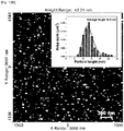
- atomic force microscopy was used to study the size distribution and surface coverage of the deposited nanoparticles.
- a soft tapping mode AFM image and height distribution histogram of the hybrid nanoparticles is presented in Fig. 1(B) and in the inset, respectively.
- the height distribution can be approximated quite well with a log-normal function (curve in the inset), having an average height of 12.5nm + - 0.2nm.
- the bright spots are aggregates of two or more nanoparticles, probably arising from the "piling up” or coalescence of two or more nanoparticles on the surface of the substrate.
- Fig. 1(C) displays a low-magnification overview high angle annular dark field (HAADF) scanning TEM (STEM) micrograph of Ag-decorated Si QDs.
- HAADF high angle annular dark field
- STEM scanning TEM
- Fig. 2(A) shows a high resolution HAADF-STEM micrograph of one nanoparticle of irregular shape, with a size of about 13nm encapsulated with an about 2 nm native oxide shell (samples were exposed to atmosphere before insertion in the TEM column).
- the Ag nanoclusters appear as dark spots, marked by numbers through 1-4.
- a TEM tilt series experiment of the same nanoparticle, as explained in detail with reference to Fig. 7 below confirmed that the Ag nanoclusters are on the surface and not embedded in the Si core.
- Both images of Figs. 2(A) and 2(B) indicate that the Si core consists of small crystalline nanograins of different crystallographic orientations.
- TEM lattice interference imaging of polycrystalline materials is fundamentally limited by the arbitrary number of grains in any given projection, and the arbitrary orientations of the crystal axes with respect to the electron beam, neither of which is known a priori.
- Great care must be taken to ensure that lattice interference patterns and associated Fourier transforms are not mis- or over-interpreted, for example as a result of misalignment, multiple-diffraction effects or Moire interference.
- the number of grains will tend to be underestimated, as many grains will not be fortuitously aligned to a sufficiently low-index crystallographic axis with respect to the electron beam, and will therefore appear devoid of crystal structure. Nevertheless, in selected cases, fortuitous structure and alignment of certain regions may allow relatively simple interpretation.
- the Si nanograin marked by the arrow shown in Fig. 7 is one such example, being fortuitously positioned with respect to the electron beam such that Si ⁇ 111 ⁇ lattice planes can easily be discerned. Multiple twinning is evident, and suggests that it belongs to the decahedral structure.
- the Fourier filtered image formed by selectively masking the nanograin then applying inverse Fourier transform to reduce the noise and enhance the contrast is shown in Figs 5 and 6 .
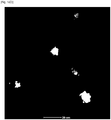
- Figs. 3(A) to 3(C) are HAADF-STEM images of nanoparticles produced under different DC magnetron powers. As shown in the figures, a low coverage was achieved by 60W magnetron power ( Fig. 3(A) ) and the coverage increased by increasing the power to 90 W ( Fig. 3(B) ) and 120W ( Fig. 3(C) ).
- the present invention provides a novel strategy for deliberately manipulating the nanostructure of freshly-nucleated quantum dots by decoration with suitable catalysts whilst still in transit from the genesis chamber to the deposition substrate.
- the present invention applies a well-known phenomenon (MIC) in thin film materials science to a previously unreported configuration, facilitating QD nanostructure control and bringing a plethora of potential applications in different fields.
- MIC well-known phenomenon
- This approach based on a modified magnetron sputter inert gas condensation technique, provides a general route for controlled MIC of semiconductor QDs, and the growth of multicomponent polycrystalline (semiconductor-core)/(metallic-subshell) nanoparticles.
- the first chamber of the UHV system is the aggregation chamber 102 where the nanoparticle beam is formed.
- This chamber contains the magnetron head 104, which is movable via a linear drive 126, and is enclosed in a coolant jacket, constantly flushed with water at 16 Celsius degrees through water provided a connection port for cool water 124.
- An Ar/He gas mix is introduced at the magnetron head 104 through the aggregation gas feed 128, and is drawn by the strong pressure differential through the aperture 130 at the other end of the chamber 102.
- the Ar serves as the sputtering gas, whilst the He is introduced as a carrier gas.
- a 1" silicon magnetron sputtering target (Si n-type, purity >99.999%, resistivity: ⁇ 0.001 Ohm-m, dimension: 25 mm diameter x 0.125" thick) was purchased from Kurt J. Lesker, PA.
- a custom-shape silver magnetron sputtering target (Ag, purity >99.99%, resistivity ⁇ 2 x 10 -8 Ohm-m, dimension: 150mm length x 50.8 mm width x 3.0 mm thick) was purchased from K. Tech. Ltd., UK.
- Undoped Si dice with (100) orientation and 5 mm x 5 mm in size for AFM measurements were purchased from mtixtl, USA.
- Carbon-coated grids (400 mesh) were purchased from Ted Pella Ltd. for TEM/STEM analysis.
- the silicon dice Prior to deposition, the silicon dice (for AFM images) were ultrasonicated in acetone, 2-propanol and deionized purified water for 5 min, respectively, and subsequently dried in a stream of high purity nitrogen.
- the Si dice surfaces exhibited typical RMS roughness of 0.17 nm (measured with contact-mode AFM). Samples of Si-core/Ag-subshell quantum dots for TEM/STEM observations were created by direct deposition onto carbon TEM grids in the UHV chamber.
- the Si nanoclusters are formed by gas phase condensation from a flux of sputtered Si atoms from a n-type Si target in an inert gas atmosphere (Ar, at a partial pressure of 70 SCCM and He, at a partial pressure of 5 SCCM) mounted inside a water cooled tube known as the aggregation zone of a NanoGen Trio ion cluster source from Mantis Deposition Ltd. as shown in Fig. 1(A) .
- the supersaturated Si vapor 120 is generated by sputtering an n-type Si target in an inert gas atmosphere (Ar, gas flow 70 SCCM and He, at a gas flow of 5 SCCM) as shown in Fig. 1(A) .
- the gas beam enters the pick-up chamber through the aperture and hits the Si ions that are evaporated by the dc magnetron.
- the Si vapors are picked up by the Ar gas molecules from the incipient beam and are condensed to yield condensed liquid Si nanoparticles 118.
- the size of the Si QDs is strictly controlled by the partial pressure inside the pick-up zone.
- the gas beam containing the cold Si clusters enters the second pick-up zone (shell coater chamber 114) through a 5mm orifice, and the Ag vapors from an Ag target on the linear magnetron sputter source 132 are embedded into the Ar gas (gas flow 10 sccm), either by forming core-shell nanoparticles or, depending on the degree of miscibility, bimetallic nanoparticles.
- the sample holder where the TEM grids and substrate 110 for depositing the nanocrystalline Si-core/Ag-subshell QDs are held, was mounted in front of the nanoparticle beam through a fast entry load lock.
- the pressure in the pick up zone in the aggregation chamber 102 was about 3.0 x 10 -1 mbar, and in the substrate deposition chamber, the base pressure was typically 7.0 x 10 -8 mbar, rising to 1.1 x 10 -3 mbar with the introduction of Ar/He during the sputtering process.
- the growth of the nanocrystalline Si-core/Ag-subshell QDs is strongly dependent on three parameters: the power applied to the magnetron, the flow rate and pressure of the aggregation gas; and the length of the aggregation zone. In this invention, these parameters were adjusted appropriately.
- the aggregation zone length was set to maximum (95 mm) by moving the magnetron head backward to the fully-retracted position.
- the nanocrystalline Si-core/Ag-subshell QDs are produced using 90 W DC power magnetron for Si target (core) and 60 W to 120W for Ag target (core-shell-coater).
- the deposition time was 40 minute and substrate holder rotation was 2 rpm.
- Atomic Force Microscopy was used for morphological characterization of the nanoparticles.
- a loadlock mechanism allowed sample transfer from the deposition UHV system, to the inert gas glovebox containing the AFM (Multimode 8, Bruker, CA), thereby avoiding atmospheric exposure.
- the AFM scanner was set on an active vibration isolation table in order to minimize the noise level and guarantee the highest resolution performance.
- the AFM scans were performed in tapping mode using commercial silicon-nitride triangular cantilever (spring constant of 0.35 N/m, resonant frequency 65 kHz) based tips with a typical radius less than 10 nm.
- the height distribution curves and root-mean-square (rms) roughness values were calculated from AFM images using the Scanning Probe Image Processor (SPIP) software (Image Metrology, Horsholm, DK).
- SPIP Scanning Probe Image Processor
- High resolution bright field (BF) and high-angle annular dark field (HAADF) imaging were carried out using an FEI Titan 300kV TEM/STEM, equipped with a probe corrector for aberration-corrected STEM imaging.
- TEM mode the spherical and chromatic aberrations were 1.2mm and 1.6mm, respectively.
- Point resolution was ⁇ 0.20nm, at Scherzer defocus conditions of -50nm to +60nm.
- STEM mode the spherical aberration was in the range 0-5 micrometers, with chromatic aberration of 1.8-2.0mm.
- Optimum STEM-HAADF resolution was approximately 0.1nm.
- Plasma cleaning of the nanocrystalline Si-core/Ag-subshell QDs was performed using commercially available plasma cleaner (E.A. Fischione, Model 1020), using a gas mixture of Ar and O 2 , in the ratio 3:1, with a 13.56 MHz oscillating field system, and expected ion energies less than 12 eV.
- Fig. 4(A) is an overview bright field TEM image of nanoparticles according to an embodiment of the present invention.
- Fig. 4(B) is a histogram showing diameter distribution of the embodiment shown in FIG. 4(A).
- Fig. 4(C) is an overview HAADF-STEM image of the nanoparticles shown in Fig. 4(A).
- Fig. 4(D) is annother overview HAADF-STEM image of the nanoparticles shown in Fig. 4(A) with a greater magnification.
- the average diameter was found to be 12.4 nm.
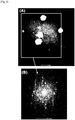
- Fig. 5 is an HAADF-STEM image of a Si-core/Ag-subshell quantum dot according to an embodiment of the present invention together with a FFT pattern.
- the FFT pattern shows that the region is polycrystalline. STEM scanning artifacts, owing to mechanical instability of the microscope, are also evident.
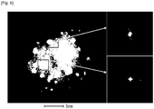
- Fig. 6 is an HAADF-STEM image of selected Ag nanoclusters on a Si-core/Ag-subshell nanopartcile according to an embodiment of the present invention together with the corresponding FFT patterns for the indicated regions.
- the FFT patterns indicate that these regions are crystalline.
- Fig. 7 shows HRTEM images of a single Si-core/Ag-subshell nanoparticle according to an embodiment of the present invention tilted at +15 degrees, 0 degrees, and -15 degrees angles, respectively. These figures further confirm that the structures of the Si-core/Ag-subshell nanoparticle as described above.
- Fig. 8(A) shows a FFT pattern from the HR TEM images of amorphous Silicon nanoparticle.
- Fig. 8(B) shows a FFT pattern from the HR TEM images of crystalline Silicon nanoparticle. As compared with the FFT patterns shown above, it is evident that the nanoparticles of the present invention have crystalline Si grains.
- Fig. 9 shows additional images of Si-core/Ag-subshell QDs (quantum dots) after plasma cleaning process according to an embodiment of the present invention
- (A) are
- (C) are bright-field images
- (B) and (D) are HAADF-STEM images, respectively.
- the images show that plasma cleaning is effective for removing Ag from the Si-core.
- Fig. 10 shows TEM images of a crystalline Si QDs covered by Ag sub shell according to an embodiment of the present invention
- (A) is a bright field image
- (B) is an HAADF-STEM image.
- Fig. 11 is a schematic illustration of the growth process of the nanocrystalline Si core-Ag subshell QDs.
- the inset shows the volume fraction of the intergrain region as a function of the grain size assuming a grain boundary thickness of 0.6 nm.
- Fig. 11 shows a phenomenological model for the evolution of nanocrystalline Si core-Ag subshell nanoparticles from amorphous Si QDs. Initially, the evaporated Si atoms nucleate into droplets, still in a liquid state above the melting temperature of Si. These particles develop a solid amorphous structure upon cooling through the melting temperature.
- the Ag atoms are released from the surface of the Ag sputtering target, and begin to interact with the amorphous Si clusters.
- Small Ag nanoclusters nucleate on the surface of the Si, as evidenced by MD simulations.
- a liquidus conjunction with Ag leads to recombine the reacting with amorphous Si surfaces and forming an amorphous- Si and Ag -subshell structure.
- the Ag clusters segregate at the surface, and both materials adopt a crystalline structure.
- the Ag seeds play the central role in increasing the crystallinity of the amorphous Si.
- the volume of atoms in the disordered grain boundaries represents an atypically large fraction of the entire nanoparticle volume.
- the subscripts in refers to the intergrain.
- the inset in Fig. 11 shows the volume fraction of the inter-grain regions as a function of grain size, calculated using Eq. 1.
- nanoparticles of the present invention will have improved physical properties like increased thermal expansion, specific heat and strength, and reduced density.
Landscapes
- Chemical & Material Sciences (AREA)
- Engineering & Computer Science (AREA)
- Organic Chemistry (AREA)
- Crystallography & Structural Chemistry (AREA)
- Materials Engineering (AREA)
- Metallurgy (AREA)
- Physics & Mathematics (AREA)
- Thermal Sciences (AREA)
- Silicon Compounds (AREA)
- Nanotechnology (AREA)
- Physical Vapour Deposition (AREA)
- Catalysts (AREA)
- Physical Deposition Of Substances That Are Components Of Semiconductor Devices (AREA)
- Inorganic Chemistry (AREA)
Description
- The present invention relates to metal induced crystallization of amorphous semiconductor, and in particular, to metal induced crystallization of amorphous semiconductor small dots and quantum dots.
- Control of crystallinity and grain structure has been a central component of advanced materials engineering and metallurgy for centuries, ranging from forging of ancient Japanese katana or swords (Non-Patent Literature No. 1) to modern nano-engineered transistor gate electrodes (Non-patent Literature Nos. 2 and 3). Mechanical, optical, magnetic and electrical properties (to name a few) can all be tailored via control of parameters like grain size, grain boundary precipitates, and crystallographic defect densities and impurities (Non-patent Literature Nos. 4-6). Metal-induced crystallization (MIC) is a phenomenon in which amorphous semiconductor materials can be crystallized at relatively low temperatures in the presence of appropriate metal catalysts (Non-patent Literature Nos. 7-8). MIC has been reported for a wide range of bulk materials with quite different material interactions (e.g., Ni, Al and Ag) (Patent-Literature No. 1 and Non-patent Literature Nos. 9-13). Metal induced crystallization (MIC) of amorphous semiconductor materials has been extensively studied due to its applications to solar cells and field effect transistors.
- The Si-Ag system has been extensively studied over the last three decades (Non-patent Literature Nos. 14-17). Notably, with 11% Si content, this binary system has a eutectic temperature around 830 Celsius degrees -845 Celsius degrees (for reference, the melting points for bulk Si and Ag are 1414 Celsius degrees and 962 Celsius degrees, respectively) (Non-patent literature No. 15). Unlike many transition metal/Si systems, the mutual solubility of Ag and Si in the solid state are negligible (Non-patent Literature No. 16), which is an important attribute. A recent study by Bokhanov and Korchagin on the amorphous-Si film/Ag particle system concisely summarizes the mechanisms governing MIC; the formation of eutectics is preceded by metal diffusion into amorphous Si with the formation of metastable silver silicide. Subsequent cooling of the system leads to the decomposition of the metastable silicide and subsequently to the evolution of polycrystalline Si and metallic Ag (Non-patent Literature No. 17).
- However, to date, these studies and development have been limited to three-dimensional bulk and two-dimensional thin films.
- [PL1]
JP 2002 2175983A -
- [NPL 1] M. Durand-Charre, "Microstructure of steels and cast iron" Springer p. 28 (2003).
- [NPL 2] X. Duan, R. Gao, P. Xie, T. Cohen-Karni, Q. Qing, H. S. Choe, B. Tian, X. Jiang, C. M. Lieber, Nature Nanotechnol.7, 174 (2012).
- [NPL 3] M. A. Green, J. Zhao, A. Wang, P. J. Reece, M. Gal, Nature 412, 805 (2001).
- [NPL 4] H. A. Atwater, A. Polman, Nature Mater. 9, 205 (2010).
- [NPL 5] W. Wang, S. Wu, K. Reinhardt, Y. Lu, S. Chen, Nano Lett. 10, 2012 (2010).
- [NPL 6] J. P. Wilcoxon, B. L. Abrams, Chem. Soc. Rev. 35, 1162 (2006).
- [NPL 7] J. D. Hwang, L. C. Luo, T. J. Hsueh, S. B. Hwang, Appl. Phys. Lett. 101, 152108 (2012).
- [NPL 8] J. A. Farmer, C. T. Campbell, Science 329, 933 (2010).
- [NPL 9] O. G. Shpyrko et al., Science 313, 77 (2006).
- [NPL 10] S. Kumagai et al., Jpn. J. Appl. Phys. 51,11PA03 (2012).
- [NPL 11] M. Itakura, S. Masumori, N. Kuwano, H. Kanno, T. Sadoh, M. Miyao, Appl. Phys. Lett. 96, 18210 (2010).
- [NPL 12] C. W. Lin, S. C. Lee, Y. S. Lee, J Mater Sci: Mater Electron 21, 270 (2010).
- [NPL 13] O. Nast, Andreas J. Hartmann, J Appl. Phys. 88, 716 (2000).
- [NPL 14] R. W. Oleslnski, A. B. Gokhale, G. J. Abbaschlan, Bulletin of Alloy Phase Diagrams 635, 10 (1989).
- [NPL 15] A. V. Nomoev and S. P. Bardakhanov, Tech. Phys. Lett. 38, 375 (2012).
- [NPL 16] J. H. Choi et al., J. Mater. Chem. 21, 13256 (2011).
- [NPL 17] B. Bokhonov, M. Korchagin, Journal of Alloys and Compound 335, 149 (2002).
- There has been no report of metal induced crystallization of amorphous silicon nanoscale small particles or quantum dots, which would be useful for various bioimaging and biosensing applications, hydrogen storage and/or optoelectronics devices.
- Accordingly, the present invention is directed to metal-induced crystallization of amorphous small-scale particles and quantum dots useful for various semiconductor engineering and fabrication.
- An object of the present invention is to provide method for performing metal-induced crystallization of amorphous small-scale particles and quantum dots and to provide resulting metal-induced crystallized nanoscale particles or quantum dots useful for various semiconductor engineering and fabrication.
- To achieve these and other advantages and in accordance with the purpose of the present invention, as embodied and broadly described, in one aspect, the present invention provides crystallinity control to the internal structure of semiconductor quantum dots (QDs) via in flight decoration and metal-induced crystallization (MIC), which, to the best of the inventor's knowledge, has not been achieved before.
- The present invention is defined in
claim 1. Optional embodiments are defined in the dependent claims. - [deleted]
- Additional or separate features and advantages of the invention will be set forth in the descriptions that follow and in part will be apparent from the description, or may be learned by practice of the invention. The objectives and other advantages of the invention will be realized and attained by the structure particularly pointed out in the written description and claims thereof as well as the appended drawings.
- It is to be understood that both the foregoing general description and the following detailed description are exemplary and explanatory, and are intended to provide further explanation of the invention as claimed.
-
- [
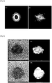
Fig. 1(A)] Fig. 1(A) is a schematic view of an advanced core-shellnanoparticle deposition system 100 used for the production of embodiments of the present invention. - [
Fig. 1(B)] Fig. 1(B) is an AFM height image of Si-Ag nanoparticles with particle height distribution of more than 1000 particles (inset) according to an embodiment of the present invention. A log-normal distribution fit to the histogram is shown in the inset. - [
fig.1(C)]Fig. 1(C) is a low resolution HAADF-STEM micrograph of Si core-Ag subshell nanoparticles according to an embodiment of the present invention. The Si core appears in gray contrast decorated with several bright Ag nanoclusters. - [
fig.2]Fig. 2 shows: (A) a high resolution HAADF-STEM micrograph of Si core-Ag subshell nanoparticles according to an embodiment of the present invention (the Si core appears in gray contrast decorated with several bright Ag nanoclusters marked by numbers 1- 4 respectively; (B) a bright-field HRTEM image of the same nanoparticle as in (A) with the same orientation under the electron beam (the Ag nanoclusters previously numbered 1-4 in the HAADF mode appear like dark spots); (C) a bright-field HRTEM image of a nanoparticle having 2 Ag nanoclusters and 2 Si grains; (D) a bright-field HRTEM image of a nanoparticle having 3 Ag nanoclusters and 3 Si grains; (E) a bright-field HRTEM image of a nanoparticle having 6 Ag nanoclusters and 6 Si grains; and (F) a bright-field HRTEM image of a nanoparticle having 8 Ag nanoclusters and 9 Si grains. The bright-field HRTEM images (C)-(F) displays the correlation between the number of nanocrystalline Si grains and the number of Ag nanoclusters on the surface. - [
fig.3]Fig. 3 shows: (A) an HAADF-STEM image of a nanoparticle produced under a DC magnetron power of 60W for Ag sputtering according to an embodiment of the present invention; (B) an HAADF-STEM image of a nanoparticle produced under a DC magnetron power of 90W for Ag sputtering according to an embodiment of the present invention; (C) an HAADF-STEM image of a nanoparticle produced under a DC magnetron power of 120W for Ag sputtering according to an embodiment of the present invention; (D) is a bright-field HRTEM image of a nanoparticle produced under a DC magnetron power of 120W after plasma cleaning process according to an embodiment of the present invention; (E) an HAADF-STEM image of the nanoparticle produced under a DC magnetron power of 120W after plasma cleaning process shown in (D); and (F) a bright-field HRTEM image of a "simple" amorphous Si QD (no Ag decoration was applied). - [
fig.4]Fig. 4 shows; (A) an overview bright field TEM image of nanoparticles according to an embodiment of the present invention; (B) a histogram showing diameter distribution of the embodiment shown in (A); (C) an overview HAADF-STEM image of the nanoparticles shown in (A); and (D) annother overview HAADF-STEM image of the nanoparticles shown in (A). - [
fig.5]Fig. 5 is an HAADF-STEM image of a Si-core/Ag-subshell nanopartcile according to an embodiment of the present invention together with a FFT pattern. [fig.6]Fig. 6 is an HAADF-STEM image of selected Ag nanoclusters on a Si-core/Ag-subshell nanopartcile according to an embodiment of the present invention together with the corresponding FFT patterns. - [
fig.7]Fig. 7 shows HRTEM images of a single Si-core/Ag-subshell tilted at +15 degrees, 0 degrees, and -15 degrees angles, respectively. - [
fig.8]Fig. 8 shows (A) a FFT pattern from the HR TEM images of amorphous Silicon nanoparticle and (B) a FFT pattern from the HR TEM images of crystalline Silicon nanoparticle. - [
fig.9]Fig. 9 shows additional images of Si-core/Ag-subshell QDs after plasma clean process according to an embodiment of the present invention; (A) and (C) are bright-field images and (B) and (D) are HAADF-STEM images, respectively. - [
fig.10]Fig. 10 shows TEM images of a crystalline Si QDs covered by Ag sub shell according to an embodiment of the present invention; (A) is a bright field image and (B) is an HAADF-STEM image. - [
fig.11]Fig. 11 is a schematic illustration of the growth process of the nanocrystalline Si core-Ag subshell QDs. The inset shows the volume fraction of the intergrain region as a function of the grain size assuming a grain boundary thickness of 0.6 nm. - In one aspect, the present invention provides controlled MIC in zero-dimensional nanostructures of amorphous silicon (Si) quantum dots for the first time, via application of silver (Ag) subshell nanoclusters to deliberately seed the crystallization process. The result is novel (nanophase Si-core)/(Ag-subshell) nanoparticles (Si core that is nanocrystalline /contains Si nanograins (crystallites)).
- In some aspects of the present invention, the final number of grains in the Si quantum dot can be controlled and is proportional to the number of Ag nanoclusters forming the subshell. After deposition of the hybrid Si-Ag system, the Ag catalysts can be left in place, or removed via plasma etch to leave an undamaged Si core of the desired crystallinity. This approach, based on a modified magnetron sputter inert gas condensation technique, provides a general route for controlled MIC of semiconductor QDs (quantum dots), and the growth of multicomponent polycrystalline (semiconductor-core)/(metallic-subshell) nanoparticles.
- These novel multicomponent nanoparticles have quite apparent applications in various technical fields, such as:
- (i) Multimodal bioimaging and biosensors (because silicon is photoluminescent while the silver is plasmonic material. Also, due to the unique structure of the hybrid particles, one can gain access to both the silicon core and the silver subshell);
- (ii) Hydrogen storage (the Si core is a nanophase material suitable for absorbing more hydrogen at the grain boundaries, while the metal can work as a catalyst to speed the process of absorption and desorption of hydrogen at relatively lower temperatures); and
- (iii) Optoelectronic devices like infrared detectors and photovoltaics owing to the unique optical properties of both core and subshell materials.
- Furthermore, in some embodiments of the present invention, due to the small dimensions of the nanophase hybrid particles described herein, the volume of atoms in the disordered grain boundaries represents an atypically large fraction of the entire nanoparticle volume. Therefore, in comparison to conventional coarse-grained polycrystalline materials with the same composition and grain size above 50 nm, in some embodiments, nanoparticles of the present invention will have improved physical properties like increased thermal expansion, specific heat and strength; and reduced density, which further expands the range of applications of this material.
- In one aspect, the present invention provides controlled MIC in a zero dimensional semiconductor (QD) system for the first time, using Si-Ag as an exemplary system. A customized gas-aggregated sputtering system is used, and Ag nanoclusters were applied as subshell seeds to induce crystallization, in-flight, of freshly-sputtered amorphous-Si QDs. This technology is applicable to other semiconductor/metal catalyst combinations, that is combinations of any one of Si, Ge, SiGe quantum dots with the metals Al, Au, Ni, Pd or Cu. As described below, molecular dynamics (MD) simulation was conducted, which well illustrates the process of Ag atom interaction and nucleation on the Si QD cores.
- In another aspect, the present invention uniquely demonstrates the dynamic and still tunable structure of freshly nucleated quantum dots whilst still en route from their nucleation chamber to their deposition substrate, and offers an exciting new dimension for controlling and engineering the crystallinity and functionality of zero dimensional semiconductor materials.
- Various embodiments of the present invention are manufactured using a modified gas-aggregated sputtering system as illustrated in
Fig. 1(A). Fig. 1(A) is a schematic view of an advanced core-shellnanoparticle deposition system 100 used for the production of embodiments of the present invention. The principles of particle formation in magnetron sputtering with inert gas condensation are well established (Non-patent literature Nos. 18 and 19). In some embodiments, a supersaturated Si vapor was generated by asputtering target material 106 on theDC magnetron head 104 mounted in a water-cooled inert-gas aggregation chamber 102. Within thisaggregation zone 112, nucleation of small liquid Si QDs (quantum dots) takes place in the (relatively high pressure) inert gas atmosphere, followed by the nucleation and growth of larger liquid Si QDs due to coalescence. The size distribution of the Si QDs can be controlled by adjusting experimental parameters, including the aggregation zone length, the aggregation chamber pressure and the magnetron power. The pressure difference between the (high pressure)aggregation zone 112 and the (low pressure)sample deposition chamber 108 transports the freshly-nucleated Si QDs through the differential-pumping aperture and out of the aggregation zone. Without further intervention, the QDs should stabilize and cool down to room temperature during transport. However, we applied an incident flux of low pressure Ag vapor to decorate the rapidly-cooling Si QDs with Ag aggregates, immediately upon exiting theaggregation zone 112. The Ag was sputtered from alinear magnetron target 132 in the coating zone 134 positioned parallel to the flight direction of the Si QD cores, en route from theaggregation zone 112 of theaggregation chamber 102 to thesample deposition chamber 108. More details are explained in respective sections below. - After substrate landing and load-lock transfer to an inert gas glovebox, atomic force microscopy (AFM) was used to study the size distribution and surface coverage of the deposited nanoparticles. A soft tapping mode AFM image and height distribution histogram of the hybrid nanoparticles is presented in
Fig. 1(B) and in the inset, respectively. The height distribution can be approximated quite well with a log-normal function (curve in the inset), having an average height of 12.5nm + - 0.2nm. The bright spots are aggregates of two or more nanoparticles, probably arising from the "piling up" or coalescence of two or more nanoparticles on the surface of the substrate. It is well-known that in AFM scans, height is a more reliable indicator of the true particle size than the lateral size; the latter being falsely inflated as a result of the convolution of the finite AFM tip size with the nanoparticle geometry. Further transmission electron microscopy (TEM), in various imaging modes, was applied to investigate the morphology and atomic structure of the deposited hybrid nanoparticles. Samples with various deposition conditions were investigated, and it is determined that simple un-decorated Si QDs were amorphous, whilst Ag-decorated Si QDs were found to be polycrystalline (nanocrystalline also called nanophase). It is also found that there is a correlation between the number of Ag "surface seeds" and the complexity of the Si internal grain structure. The average diameter of the nanoparticles, estimated by the low-magnification TEM images (Figs. 4(A)-4(D) to be discussed below), is consistent with the AFM results (Fig. 1(B) ). -
Fig. 1(C) displays a low-magnification overview high angle annular dark field (HAADF) scanning TEM (STEM) micrograph of Ag-decorated Si QDs. The Si core appears gray, decorated with several bright Ag nanoclusters in line with the atomic number or Z-contrast expected from this imaging mode. -
Fig. 2(A) shows a high resolution HAADF-STEM micrograph of one nanoparticle of irregular shape, with a size of about 13nm encapsulated with an about 2 nm native oxide shell (samples were exposed to atmosphere before insertion in the TEM column). High-resolution TEM (HRTEM) image of the same nanoparticle, with unchanged orientation with respect to the electron beam, is shown inFig. 2(B) (offering complementary contrast mechanisms). The Ag nanoclusters appear as dark spots, marked by numbers through 1-4. A TEM tilt series experiment of the same nanoparticle, as explained in detail with reference toFig. 7 below confirmed that the Ag nanoclusters are on the surface and not embedded in the Si core. Both images ofFigs. 2(A) and 2(B) indicate that the Si core consists of small crystalline nanograins of different crystallographic orientations. - TEM lattice interference imaging of polycrystalline materials is fundamentally limited by the arbitrary number of grains in any given projection, and the arbitrary orientations of the crystal axes with respect to the electron beam, neither of which is known a priori. Great care must be taken to ensure that lattice interference patterns and associated Fourier transforms are not mis- or over-interpreted, for example as a result of misalignment, multiple-diffraction effects or Moire interference. In general, the number of grains will tend to be underestimated, as many grains will not be fortuitously aligned to a sufficiently low-index crystallographic axis with respect to the electron beam, and will therefore appear devoid of crystal structure. Nevertheless, in selected cases, fortuitous structure and alignment of certain regions may allow relatively simple interpretation.
- The Si nanograin marked by the arrow shown in
Fig. 7 is one such example, being fortuitously positioned with respect to the electron beam such that Si {111} lattice planes can easily be discerned. Multiple twinning is evident, and suggests that it belongs to the decahedral structure. For clarity, the Fourier filtered image formed by selectively masking the nanograin then applying inverse Fourier transform to reduce the noise and enhance the contrast (i.e., FFT pattern) is shown inFigs 5 and6 . Most of the Ag nanoclusters on the surface have uniform spherical shape, and exhibit interference patterns which, although non-trivial to quantitatively interpret because of superposition with underlying Si grain lattice(s), provide proof that the Ag nanoclusters are also crystalline. - As mentioned briefly above, a general correlation between the number of crystalline Si grains in the QD core and the number of Ag nanoclusters on the surface was found. This is demonstrated in
Fig. 2(C) (two Ag nanocluster and two Si nanograins in the core),Fig. 2(D) (three Ag nanoclusters and three Si nanograins),Fig. 2(E) (six Ag nanoclusters and six Si nanograins), andFig. 2(F) (eight Ag nanoclusters and nine nanograins), respectively. Therefore, the more Ag nanoclusters, the more Si nanograins. - Furthermore, it is possible to control the number of Ag nanoclusters nucleating on the Si core by adjusting the power of the Ag
magnetron sputter source 132.Figs. 3(A) to 3(C) are HAADF-STEM images of nanoparticles produced under different DC magnetron powers. As shown in the figures, a low coverage was achieved by 60W magnetron power (Fig. 3(A) ) and the coverage increased by increasing the power to 90 W (Fig. 3(B) ) and 120W (Fig. 3(C) ). - The immiscibility of Si and Ag was briefly mentioned above. The image in
Fig. 2A shows segregated Si and Ag regions, with no evidence of intermixing between the low-Z semiconductor and high-Z metal. This observation was further supported by plasma cleaning of the sample to remove the Ag, with the nanocrystalline Si core left intact. Examples after plasma cleaning are shown in the HAADF-STEM micrograph ofFig. 3E and the bright-field HRTEM image ofFig. 3D and inFig. 9 . As shown in these figures, substantially all Ag regions are removed by plasma cleaning. This gives an additional degree of freedom in nanoparticle fabrication; one may retain the hybrid structure if advantageous for a given application, or may selectively remove the catalyst to leave only the core behind. - The present invention provides a novel strategy for deliberately manipulating the nanostructure of freshly-nucleated quantum dots by decoration with suitable catalysts whilst still in transit from the genesis chamber to the deposition substrate. The present invention applies a well-known phenomenon (MIC) in thin film materials science to a previously unreported configuration, facilitating QD nanostructure control and bringing a plethora of potential applications in different fields. This approach, based on a modified magnetron sputter inert gas condensation technique, provides a general route for controlled MIC of semiconductor QDs, and the growth of multicomponent polycrystalline (semiconductor-core)/(metallic-subshell) nanoparticles.
- More details of the equipment and the evaluations of embodiments of the present invention are described below while some descriptions below overlap the above descriptions.
- A UHV deposition system (Mantis Deposition Ltd, UK) was used for the production of the amorphous (a) Si and nanocrystalline Si-core/Ag-subshell quantum dots (QDs). The first chamber of the UHV system is the
aggregation chamber 102 where the nanoparticle beam is formed. This chamber contains themagnetron head 104, which is movable via alinear drive 126, and is enclosed in a coolant jacket, constantly flushed with water at 16 Celsius degrees through water provided a connection port forcool water 124. An Ar/He gas mix is introduced at themagnetron head 104 through theaggregation gas feed 128, and is drawn by the strong pressure differential through theaperture 130 at the other end of thechamber 102. The Ar serves as the sputtering gas, whilst the He is introduced as a carrier gas. - A 1" silicon magnetron sputtering target (Si n-type, purity >99.999%, resistivity: <0.001 Ohm-m, dimension: 25 mm diameter x 0.125" thick) was purchased from Kurt J. Lesker, PA. A custom-shape silver magnetron sputtering target (Ag, purity >99.99%, resistivity∼ 2 x 10⁻⁸ Ohm-m, dimension: 150mm length x 50.8 mm width x 3.0 mm thick) was purchased from K. Tech. Ltd., UK. Undoped Si dice with (100) orientation and 5 mm x 5 mm in size for AFM measurements were purchased from mtixtl, USA. Carbon-coated grids (400 mesh) were purchased from Ted Pella Ltd. for TEM/STEM analysis.
- Prior to deposition, the silicon dice (for AFM images) were ultrasonicated in acetone, 2-propanol and deionized purified water for 5 min, respectively, and subsequently dried in a stream of high purity nitrogen. The Si dice surfaces exhibited typical RMS roughness of 0.17 nm (measured with contact-mode AFM). Samples of Si-core/Ag-subshell quantum dots for TEM/STEM observations were created by direct deposition onto carbon TEM grids in the UHV chamber.
- First, the Si nanoclusters are formed by gas phase condensation from a flux of sputtered Si atoms from a n-type Si target in an inert gas atmosphere (Ar, at a partial pressure of 70 SCCM and He, at a partial pressure of 5 SCCM) mounted inside a water cooled tube known as the aggregation zone of a NanoGen Trio ion cluster source from Mantis Deposition Ltd. as shown in
Fig. 1(A) . Thesupersaturated Si vapor 120 is generated by sputtering an n-type Si target in an inert gas atmosphere (Ar, gas flow 70 SCCM and He, at a gas flow of 5 SCCM) as shown inFig. 1(A) . The gas beam enters the pick-up chamber through the aperture and hits the Si ions that are evaporated by the dc magnetron. The Si vapors are picked up by the Ar gas molecules from the incipient beam and are condensed to yield condensedliquid Si nanoparticles 118. The size of the Si QDs is strictly controlled by the partial pressure inside the pick-up zone. The gas beam containing the cold Si clusters enters the second pick-up zone (shell coater chamber 114) through a 5mm orifice, and the Ag vapors from an Ag target on the linearmagnetron sputter source 132 are embedded into the Ar gas (gas flow 10 sccm), either by forming core-shell nanoparticles or, depending on the degree of miscibility, bimetallic nanoparticles. The sample holder, where the TEM grids andsubstrate 110 for depositing the nanocrystalline Si-core/Ag-subshell QDs are held, was mounted in front of the nanoparticle beam through a fast entry load lock. The pressure in the pick up zone in theaggregation chamber 102 was about 3.0 x 10⁻¹ mbar, and in the substrate deposition chamber, the base pressure was typically 7.0 x 10⁻⁸ mbar, rising to 1.1 x 10⁻³ mbar with the introduction of Ar/He during the sputtering process. - The growth of the nanocrystalline Si-core/Ag-subshell QDs is strongly dependent on three parameters: the power applied to the magnetron, the flow rate and pressure of the aggregation gas; and the length of the aggregation zone. In this invention, these parameters were adjusted appropriately. The aggregation zone length was set to maximum (95 mm) by moving the magnetron head backward to the fully-retracted position. In some embodiments, the nanocrystalline Si-core/Ag-subshell QDs are produced using 90 W DC power magnetron for Si target (core) and 60 W to 120W for Ag target (core-shell-coater). The deposition time was 40 minute and substrate holder rotation was 2 rpm.
- Atomic Force Microscopy (AFM) was used for morphological characterization of the nanoparticles. A loadlock mechanism allowed sample transfer from the deposition UHV system, to the inert gas glovebox containing the AFM (Multimode 8, Bruker, CA), thereby avoiding atmospheric exposure. A controlled N2 environment inside the glovebox ensured < = 0.1 ppm oxygen and moisture levels, while allowing scanning of the samples using different AFM modes. The AFM scanner was set on an active vibration isolation table in order to minimize the noise level and guarantee the highest resolution performance. The AFM scans were performed in tapping mode using commercial silicon-nitride triangular cantilever (spring constant of 0.35 N/m, resonant frequency 65 kHz) based tips with a typical radius less than 10 nm. The height distribution curves and root-mean-square (rms) roughness values were calculated from AFM images using the Scanning Probe Image Processor (SPIP) software (Image Metrology, Horsholm, DK).
- High resolution bright field (BF) and high-angle annular dark field (HAADF) imaging were carried out using an FEI Titan 300kV TEM/STEM, equipped with a probe corrector for aberration-corrected STEM imaging. In TEM mode, the spherical and chromatic aberrations were 1.2mm and 1.6mm, respectively. Point resolution was ∼0.20nm, at Scherzer defocus conditions of -50nm to +60nm. In STEM mode, the spherical aberration was in the range 0-5 micrometers, with chromatic aberration of 1.8-2.0mm. Optimum STEM-HAADF resolution was approximately 0.1nm.
- As described above, some samples were plasma cleaned while mounted in the TEM holder, allowing TEM imaging of the same samples before and after the plasma cleaning. Plasma cleaning of the nanocrystalline Si-core/Ag-subshell QDs was performed using commercially available plasma cleaner (E.A. Fischione, Model 1020), using a gas mixture of Ar and O2, in the ratio 3:1, with a 13.56 MHz oscillating field system, and expected ion energies less than 12 eV.
-
Fig. 4(A) is an overview bright field TEM image of nanoparticles according to an embodiment of the present invention.Fig. 4(B) is a histogram showing diameter distribution of the embodiment shown inFIG. 4(A). Fig. 4(C) is an overview HAADF-STEM image of the nanoparticles shown inFig. 4(A). Fig. 4(D) is annother overview HAADF-STEM image of the nanoparticles shown inFig. 4(A) with a greater magnification. As shown in the figures, in this embodiment, the average diameter was found to be 12.4 nm. -
Fig. 5 is an HAADF-STEM image of a Si-core/Ag-subshell quantum dot according to an embodiment of the present invention together with a FFT pattern. The FFT pattern shows that the region is polycrystalline. STEM scanning artifacts, owing to mechanical instability of the microscope, are also evident. -
Fig. 6 is an HAADF-STEM image of selected Ag nanoclusters on a Si-core/Ag-subshell nanopartcile according to an embodiment of the present invention together with the corresponding FFT patterns for the indicated regions. The FFT patterns indicate that these regions are crystalline. -
Fig. 7 shows HRTEM images of a single Si-core/Ag-subshell nanoparticle according to an embodiment of the present invention tilted at +15 degrees, 0 degrees, and -15 degrees angles, respectively. These figures further confirm that the structures of the Si-core/Ag-subshell nanoparticle as described above. -
Fig. 8(A) shows a FFT pattern from the HR TEM images of amorphous Silicon nanoparticle.Fig. 8(B) shows a FFT pattern from the HR TEM images of crystalline Silicon nanoparticle. As compared with the FFT patterns shown above, it is evident that the nanoparticles of the present invention have crystalline Si grains. -
Fig. 9 shows additional images of Si-core/Ag-subshell QDs (quantum dots) after plasma cleaning process according to an embodiment of the present invention; (A) are (C) are bright-field images and (B) and (D) are HAADF-STEM images, respectively. As described above, the images show that plasma cleaning is effective for removing Ag from the Si-core. -
Fig. 10 shows TEM images of a crystalline Si QDs covered by Ag sub shell according to an embodiment of the present invention; (A) is a bright field image and (B) is an HAADF-STEM image. These images also confirm the characteristics of the nanoscale crystallized Si particle covered by Ag sub shell, as described above. -
Fig. 11 is a schematic illustration of the growth process of the nanocrystalline Si core-Ag subshell QDs. The inset shows the volume fraction of the intergrain region as a function of the grain size assuming a grain boundary thickness of 0.6 nm.Fig. 11 shows a phenomenological model for the evolution of nanocrystalline Si core-Ag subshell nanoparticles from amorphous Si QDs. Initially, the evaporated Si atoms nucleate into droplets, still in a liquid state above the melting temperature of Si. These particles develop a solid amorphous structure upon cooling through the melting temperature. - Meanwhile, Ag atoms are released from the surface of the Ag sputtering target, and begin to interact with the amorphous Si clusters. Small Ag nanoclusters nucleate on the surface of the Si, as evidenced by MD simulations. Given the eutectic nature of this material set, a liquidus conjunction with Ag leads to recombine the reacting with amorphous Si surfaces and forming an amorphous- Si and Ag -subshell structure. Upon cooling below the eutectic temperature, the Ag clusters segregate at the surface, and both materials adopt a crystalline structure. Here, the Ag seeds play the central role in increasing the crystallinity of the amorphous Si.
- Due to the small dimensions of the nanophase particles described in this invention, the volume of atoms in the disordered grain boundaries represents an atypically large fraction of the entire nanoparticle volume. Assuming a regular tetracaidecahedral grain shape model corresponding to the decahedral structure of the Si grains, with a smaller axis "d" referring to as the grain size, and a shell of thickness "s" as the grain boundary part, the volume fraction of the inter-grain regions is given by:

- Here, the subscripts in refers to the intergrain. The inset in
Fig. 11 shows the volume fraction of the inter-grain regions as a function of grain size, calculated using Eq. 1. According to this model with a grain size of the order of the average diameter of our nanoparticles, the volume fraction of the intergrain region is 27%, while at d = 6nm, about a half of the average diameter of the nanoparticle. The volume fraction increases to 60% for d = 2.4nm; the volume fraction of the intergrain region is about 50% of the volume of the particle. So, in comparison to conventional coarse-grained polycrystalline materials with the same composition and grain size above 50 nm, nanoparticles of the present invention will have improved physical properties like increased thermal expansion, specific heat and strength, and reduced density. -
- 100 Deposition System
- 102 Aggregation Chamber
- 104 Magnetron Head (DC Magnetron)
- 106 Sputtering Target Material
- 108 Sample Deposition Chamber
- 110 Substrate
- 112 Aggregation Zone (Nanoparticles Beam Source)
- 114 Shell Coater Chamber
- 116 Silver Vapor
- 118 Condensed Liquid Si NanoParticles
- 120 Super-saturated Si Vapor
- 122 Connection Ports for Water and Gas
- 124 Connection Port for Cool Water
- 126 Linear Drive to Move DC Magnetron
- 128 Aggregation Gas Feed
- 130 Aperture
- 132 Linear Magnetron Sputter Source (Silver)
Claims (7)
- A method of forming crystallized semiconductor particles, comprising:generating vapor of any one of silicon (Si), germanium (Ge) and silicon-germanium (SiGe) in a vacuumed aggregation chamber;transporting the vapor in the vacuumed aggregation chamber towards a vacuumed deposition chamber within which a substrate is held;condensing the vapor into condensed liquid nanoparticles during the transporting of the vapor;forming amorphous semiconductor particles in the vacuumed aggregation chamber by cooling the liquid nanoparticles;transporting the amorphous semiconductor particles formed in the vacuumed aggregation chamber to the vacuumed deposition chamber; andapplying a vapor of a metal catalyst of any one of silver (Ag), aluminum (Al), gold (Au), nickel (Ni), palladium (Pd) and copper (Cu) to the amorphous semiconductor particles while still in transit to the substrate in the vacuumed deposition chamber to induce crystallization of at least a portion of the amorphous semiconductor particles via the metal catalyst in the transit, thereby depositing the crystallized semiconductor particles with the metal catalyst attached thereto onto the substrate.
- The method according to claim 1, wherein the amorphous semiconductor particles are amorphous silicon particles having a dimension in the order of nanometers.
- The method according to claim 1, wherein the metal catalyst is silver (Ag).
- The method according to claim 1, further comprising performing plasma cleaning on the crystallized semiconductor particles to substantially remove the metal catalyst.
- The method according to claim 1, wherein the step of applying a vapor of a metal catalyst to the amorphous semiconductor particles includes generating the vapor of the metal catalyst by linear magnetron sputtering.
- The method according to claim 5, wherein the step of generating the vapor of the metal catalyst includes adjusting a power of the linear magnetron sputtering such that a desired number of dots made of the metal catalyst is formed on the semiconductor particles on average.
- The method according to claim 1, wherein the step of applying a vapor of a metal catalyst to the amorphous semiconductor particles includes forming dots made of the metal catalyst on the amorphous semiconductor particles such that the number of dots on respective semiconductor particles substantially corresponds to the number of crystalline grains in respective resulting poly-crystallized semiconductor particles.
Applications Claiming Priority (2)
| Application Number | Priority Date | Filing Date | Title |
|---|---|---|---|
| US201361778967P | 2013-03-13 | 2013-03-13 | |
| PCT/JP2014/001293 WO2014141662A1 (en) | 2013-03-13 | 2014-03-07 | Metal induced nanocrystallization of amorphous semiconductor quantum dots |
Publications (3)
| Publication Number | Publication Date |
|---|---|
| EP2973660A1 EP2973660A1 (en) | 2016-01-20 |
| EP2973660A4 EP2973660A4 (en) | 2016-10-19 |
| EP2973660B1 true EP2973660B1 (en) | 2017-11-01 |
Family
ID=51536341
Family Applications (1)
| Application Number | Title | Priority Date | Filing Date |
|---|---|---|---|
| EP14762623.8A Active EP2973660B1 (en) | 2013-03-13 | 2014-03-07 | Metal induced nanocrystallization of amorphous semiconductor quantum dots |
Country Status (7)
| Country | Link |
|---|---|
| US (1) | US9633842B2 (en) |
| EP (1) | EP2973660B1 (en) |
| JP (1) | JP6101977B2 (en) |
| KR (1) | KR101757570B1 (en) |
| CN (1) | CN105051864B (en) |
| CA (1) | CA2900449C (en) |
| WO (1) | WO2014141662A1 (en) |
Families Citing this family (2)
| Publication number | Priority date | Publication date | Assignee | Title |
|---|---|---|---|---|
| US10669477B2 (en) | 2016-11-08 | 2020-06-02 | Industrial Technology Research Institute | Quantum dot and method for manufacturing the same |
| CN111188006B (en) * | 2020-01-08 | 2021-07-06 | 电子科技大学 | A kind of preparation method of periodically arranged micro-nano metal particles |
Family Cites Families (22)
| Publication number | Priority date | Publication date | Assignee | Title |
|---|---|---|---|---|
| JP3562588B2 (en) | 1993-02-15 | 2004-09-08 | 株式会社半導体エネルギー研究所 | Method for manufacturing semiconductor device |
| US5275851A (en) | 1993-03-03 | 1994-01-04 | The Penn State Research Foundation | Low temperature crystallization and patterning of amorphous silicon films on electrically insulating substrates |
| TW355845B (en) | 1995-03-27 | 1999-04-11 | Semiconductor Energy Lab Co Ltd | Semiconductor device and a method of manufacturing the same |
| US6100562A (en) | 1996-03-17 | 2000-08-08 | Semiconductor Energy Laboratory Co., Ltd. | Method of manufacturing a semiconductor device |
| JP3976828B2 (en) | 1997-02-17 | 2007-09-19 | 株式会社半導体エネルギー研究所 | Method for producing crystalline silicon film |
| JP3425392B2 (en) | 1999-05-27 | 2003-07-14 | シャープ株式会社 | Method for manufacturing semiconductor device |
| US6313015B1 (en) | 1999-06-08 | 2001-11-06 | City University Of Hong Kong | Growth method for silicon nanowires and nanoparticle chains from silicon monoxide |
| JP2002175983A (en) | 2000-12-05 | 2002-06-21 | Mitsubishi Heavy Ind Ltd | Thin-film polycrystalline silicon, method of manufacturing the same and silicon photoelectric conversion element |
| US7306823B2 (en) | 2004-09-18 | 2007-12-11 | Nanosolar, Inc. | Coated nanoparticles and quantum dots for solution-based fabrication of photovoltaic cells |
| GB0404442D0 (en) | 2004-02-27 | 2004-03-31 | Trackdale Ltd | Composite quantum dot structures |
| KR100814454B1 (en) | 2004-03-26 | 2008-03-17 | 닛신덴키 가부시키 가이샤 | Method and apparatus for forming silicon dots |
| US20060172555A1 (en) | 2005-02-01 | 2006-08-03 | Sharp Laboratories Of America, Inc. | Method to make silicon nanoparticle from silicon rich-oxide by DC reactive sputtering for electroluminescence application |
| JP4734944B2 (en) | 2005-02-02 | 2011-07-27 | セイコーエプソン株式会社 | Method for manufacturing thin film semiconductor device |
| EP1917101A4 (en) | 2005-06-24 | 2012-02-08 | Univ Washington State Res Fdn | PROCESS FOR MANUFACTURING AND COATING NANOSTRUCTURED COMPONENTS |
| JP4497068B2 (en) | 2005-09-26 | 2010-07-07 | 日新電機株式会社 | Silicon dot forming method and silicon dot forming apparatus |
| KR20070044879A (en) | 2005-10-26 | 2007-05-02 | 주식회사 피앤아이 | Method for forming powder and uniformly vacuum deposited metal, alloy and ceramic nanoparticles and apparatus for manufacturing same |
| US8093474B2 (en) | 2007-03-23 | 2012-01-10 | Lawrence Livermore National Security, Llc | Metallic nanospheres embedded in nanowires initiated on nanostructures and methods for synthesis thereof |
| WO2009025955A1 (en) * | 2007-08-23 | 2009-02-26 | University Of Virginia Patent Foundation | Immobilized metallic nanoparticles as unique materials for therapeutic and biosensor applications |
| JP2010080827A (en) | 2008-09-29 | 2010-04-08 | Toshiba Corp | Nonvolatile semiconductor memory, and method of manufacturing the same |
| CN101736354B (en) * | 2008-11-06 | 2011-11-16 | 北京有色金属研究总院 | Method for preparing one or more of silicon nano power, silicon nanowires and silicon nanotubes by electrochemical method |
| DE102011008263A1 (en) | 2011-01-11 | 2012-07-12 | Fraunhofer-Gesellschaft zur Förderung der angewandten Forschung e.V. | Process for producing a silicon layer |
| JP2012232869A (en) | 2011-04-28 | 2012-11-29 | Toho Zinc Co Ltd | Method for producing silicon/formation auxiliary composite powder and method for producing polycrystalline silicon sintered compact |
-
2014
- 2014-03-07 EP EP14762623.8A patent/EP2973660B1/en active Active
- 2014-03-07 CA CA2900449A patent/CA2900449C/en active Active
- 2014-03-07 JP JP2015542082A patent/JP6101977B2/en active Active
- 2014-03-07 CN CN201480013680.9A patent/CN105051864B/en active Active
- 2014-03-07 WO PCT/JP2014/001293 patent/WO2014141662A1/en not_active Ceased
- 2014-03-07 KR KR1020157024266A patent/KR101757570B1/en active Active
- 2014-03-07 US US14/774,226 patent/US9633842B2/en active Active
Non-Patent Citations (1)
| Title |
|---|
| None * |
Also Published As
| Publication number | Publication date |
|---|---|
| US9633842B2 (en) | 2017-04-25 |
| CA2900449A1 (en) | 2014-09-18 |
| KR101757570B1 (en) | 2017-07-12 |
| WO2014141662A1 (en) | 2014-09-18 |
| JP6101977B2 (en) | 2017-03-29 |
| JP2016516286A (en) | 2016-06-02 |
| CN105051864A (en) | 2015-11-11 |
| KR20150144742A (en) | 2015-12-28 |
| EP2973660A1 (en) | 2016-01-20 |
| EP2973660A4 (en) | 2016-10-19 |
| US20160042948A1 (en) | 2016-02-11 |
| CA2900449C (en) | 2018-02-06 |
| CN105051864B (en) | 2017-09-12 |
Similar Documents
| Publication | Publication Date | Title |
|---|---|---|
| Tchernycheva et al. | Temperature conditions for GaAs nanowire formation by Au-assisted molecular beam epitaxy | |
| Hofmann et al. | Gold catalyzed growth of silicon nanowires by plasma enhanced chemical vapor deposition | |
| US20100065810A1 (en) | Method Of Synthesizing Semiconductor Nanostructures And Nanostructures Synthesized By The Method | |
| Patsha et al. | Seeded-growth of WS 2 atomic layers: the effect on chemical and optical properties | |
| Zhang et al. | Tracking the atomic pathways of Pt3Ni-Ni (OH) 2 core-shell structures at the gas-liquid interface by in-situ liquid cell TEM | |
| Qian et al. | FeWO4/FeS core/shell nanorods fabricated by thermal evaporation | |
| Wang et al. | Low-pressure thermal chemical vapour deposition of molybdenum oxide nanorods | |
| Zhang et al. | Role of catalyst in controlling the growth and morphology of one-dimensional SiC nanostructures | |
| US9633842B2 (en) | Metal induced nanocrystallization of amorphous semiconductor quantum dots | |
| Wang et al. | Synthesis of gram-scale germanium nanocrystals by a low-temperature inverse micelle solvothermal route | |
| Zannier et al. | Tuning the growth mode of nanowires via the interaction among seeds, substrates and beam fluxes | |
| Sutter et al. | Formation and stabilization of single-crystalline metastable AuGe phases in Ge nanowires | |
| Haapamaki et al. | Facilitating growth of InAs–InP core–shell nanowires through the introduction of Al | |
| Yildirim | Efficient vapor-liquid-solid synthesis of copper doped zinc oxide (Cu: ZnO) nanonails with highly homogeneous dopant distribution | |
| Guo et al. | Metal-layer-assisted coalescence of Au nanoparticles and its effect on diameter control in vapor-liquid-solid growth of oxide nanowires | |
| André et al. | Optical and structural analysis of ultra-long GaAs nanowires after nitrogen-plasma passivation | |
| George et al. | Optical and electrical properties of colloidal (spherical Au)-(spinel ferrite nanorod) heterostructures | |
| Chung et al. | Thermally induced formation of SiC nanoparticles from Si/C/Si multilayers deposited by ultra-high-vacuum ion beam sputtering | |
| Cheng et al. | Interfaces determine the nucleation and growth of large NbS 2 single crystals | |
| Milanova et al. | GaSb nanowires grown on a Si substrate and nanolaminatate TiO2/Ag/TiO2 structure | |
| Tham et al. | Applications of electron microscopy to the characterization of semiconductor nanowires | |
| Lee et al. | Growth of single crystal GaAs nanowires by a surface diffusion-mediated solid-liquid-solid process | |
| Wu et al. | Unusually-high growth rate (∼ 2.8 μm/s) of germania nanowires and its hierarchical structures by an in-situ continuous precursor supply | |
| Wakayama et al. | Fabrication of nanoscale heterojunction of si/au and si/ag by surface droplet epitaxy | |
| Heggen et al. | Interparticle heterostructures by spontaneous formation of Dirac nodal arc semimetal PtSn4 domains in nanoparticles produced by Supersonic Cluster Beam Deposition |
Legal Events
| Date | Code | Title | Description |
|---|---|---|---|
| PUAI | Public reference made under article 153(3) epc to a published international application that has entered the european phase |
Free format text: ORIGINAL CODE: 0009012 |
|
| 17P | Request for examination filed |
Effective date: 20150811 |
|
| AK | Designated contracting states |
Kind code of ref document: A1 Designated state(s): AL AT BE BG CH CY CZ DE DK EE ES FI FR GB GR HR HU IE IS IT LI LT LU LV MC MK MT NL NO PL PT RO RS SE SI SK SM TR |
|
| AX | Request for extension of the european patent |
Extension state: BA ME |
|
| DAX | Request for extension of the european patent (deleted) | ||
| RIN1 | Information on inventor provided before grant (corrected) |
Inventor name: SINGH, VIDYA DHAR Inventor name: CASSIDY, CATHAL Inventor name: SOWWAN, MUKHLES IBRAHIM |
|
| A4 | Supplementary search report drawn up and despatched |
Effective date: 20160916 |
|
| RIC1 | Information provided on ipc code assigned before grant |
Ipc: H01L 21/203 20060101AFI20160912BHEP Ipc: C01B 33/021 20060101ALI20160912BHEP Ipc: H01L 29/16 20060101ALI20160912BHEP Ipc: H01L 21/02 20060101ALI20160912BHEP Ipc: C30B 29/06 20060101ALI20160912BHEP Ipc: H01L 29/04 20060101ALI20160912BHEP Ipc: C01B 33/02 20060101ALI20160912BHEP Ipc: C30B 29/60 20060101ALI20160912BHEP Ipc: C30B 28/02 20060101ALI20160912BHEP Ipc: H01L 29/06 20060101ALI20160912BHEP Ipc: C30B 1/02 20060101ALI20160912BHEP |
|
| GRAP | Despatch of communication of intention to grant a patent |
Free format text: ORIGINAL CODE: EPIDOSNIGR1 |
|
| STAA | Information on the status of an ep patent application or granted ep patent |
Free format text: STATUS: GRANT OF PATENT IS INTENDED |
|
| INTG | Intention to grant announced |
Effective date: 20170522 |
|
| GRAS | Grant fee paid |
Free format text: ORIGINAL CODE: EPIDOSNIGR3 |
|
| GRAA | (expected) grant |
Free format text: ORIGINAL CODE: 0009210 |
|
| STAA | Information on the status of an ep patent application or granted ep patent |
Free format text: STATUS: THE PATENT HAS BEEN GRANTED |
|
| AK | Designated contracting states |
Kind code of ref document: B1 Designated state(s): AL AT BE BG CH CY CZ DE DK EE ES FI FR GB GR HR HU IE IS IT LI LT LU LV MC MK MT NL NO PL PT RO RS SE SI SK SM TR |
|
| REG | Reference to a national code |
Ref country code: GB Ref legal event code: FG4D |
|
| REG | Reference to a national code |
Ref country code: CH Ref legal event code: EP Ref country code: AT Ref legal event code: REF Ref document number: 942819 Country of ref document: AT Kind code of ref document: T Effective date: 20171115 |
|
| REG | Reference to a national code |
Ref country code: IE Ref legal event code: FG4D |
|
| REG | Reference to a national code |
Ref country code: DE Ref legal event code: R096 Ref document number: 602014016650 Country of ref document: DE |
|
| REG | Reference to a national code |
Ref country code: NL Ref legal event code: MP Effective date: 20171101 |
|
| REG | Reference to a national code |
Ref country code: FR Ref legal event code: PLFP Year of fee payment: 5 |
|
| REG | Reference to a national code |
Ref country code: LT Ref legal event code: MG4D |
|
| REG | Reference to a national code |
Ref country code: AT Ref legal event code: MK05 Ref document number: 942819 Country of ref document: AT Kind code of ref document: T Effective date: 20171101 |
|
| PG25 | Lapsed in a contracting state [announced via postgrant information from national office to epo] |
Ref country code: NO Free format text: LAPSE BECAUSE OF FAILURE TO SUBMIT A TRANSLATION OF THE DESCRIPTION OR TO PAY THE FEE WITHIN THE PRESCRIBED TIME-LIMIT Effective date: 20180201 Ref country code: LT Free format text: LAPSE BECAUSE OF FAILURE TO SUBMIT A TRANSLATION OF THE DESCRIPTION OR TO PAY THE FEE WITHIN THE PRESCRIBED TIME-LIMIT Effective date: 20171101 Ref country code: NL Free format text: LAPSE BECAUSE OF FAILURE TO SUBMIT A TRANSLATION OF THE DESCRIPTION OR TO PAY THE FEE WITHIN THE PRESCRIBED TIME-LIMIT Effective date: 20171101 Ref country code: ES Free format text: LAPSE BECAUSE OF FAILURE TO SUBMIT A TRANSLATION OF THE DESCRIPTION OR TO PAY THE FEE WITHIN THE PRESCRIBED TIME-LIMIT Effective date: 20171101 Ref country code: SE Free format text: LAPSE BECAUSE OF FAILURE TO SUBMIT A TRANSLATION OF THE DESCRIPTION OR TO PAY THE FEE WITHIN THE PRESCRIBED TIME-LIMIT Effective date: 20171101 Ref country code: FI Free format text: LAPSE BECAUSE OF FAILURE TO SUBMIT A TRANSLATION OF THE DESCRIPTION OR TO PAY THE FEE WITHIN THE PRESCRIBED TIME-LIMIT Effective date: 20171101 |
|
| PG25 | Lapsed in a contracting state [announced via postgrant information from national office to epo] |
Ref country code: GR Free format text: LAPSE BECAUSE OF FAILURE TO SUBMIT A TRANSLATION OF THE DESCRIPTION OR TO PAY THE FEE WITHIN THE PRESCRIBED TIME-LIMIT Effective date: 20180202 Ref country code: HR Free format text: LAPSE BECAUSE OF FAILURE TO SUBMIT A TRANSLATION OF THE DESCRIPTION OR TO PAY THE FEE WITHIN THE PRESCRIBED TIME-LIMIT Effective date: 20171101 Ref country code: IS Free format text: LAPSE BECAUSE OF FAILURE TO SUBMIT A TRANSLATION OF THE DESCRIPTION OR TO PAY THE FEE WITHIN THE PRESCRIBED TIME-LIMIT Effective date: 20180301 Ref country code: RS Free format text: LAPSE BECAUSE OF FAILURE TO SUBMIT A TRANSLATION OF THE DESCRIPTION OR TO PAY THE FEE WITHIN THE PRESCRIBED TIME-LIMIT Effective date: 20171101 Ref country code: BG Free format text: LAPSE BECAUSE OF FAILURE TO SUBMIT A TRANSLATION OF THE DESCRIPTION OR TO PAY THE FEE WITHIN THE PRESCRIBED TIME-LIMIT Effective date: 20180201 Ref country code: LV Free format text: LAPSE BECAUSE OF FAILURE TO SUBMIT A TRANSLATION OF THE DESCRIPTION OR TO PAY THE FEE WITHIN THE PRESCRIBED TIME-LIMIT Effective date: 20171101 Ref country code: AT Free format text: LAPSE BECAUSE OF FAILURE TO SUBMIT A TRANSLATION OF THE DESCRIPTION OR TO PAY THE FEE WITHIN THE PRESCRIBED TIME-LIMIT Effective date: 20171101 |
|
| PG25 | Lapsed in a contracting state [announced via postgrant information from national office to epo] |
Ref country code: CZ Free format text: LAPSE BECAUSE OF FAILURE TO SUBMIT A TRANSLATION OF THE DESCRIPTION OR TO PAY THE FEE WITHIN THE PRESCRIBED TIME-LIMIT Effective date: 20171101 Ref country code: SK Free format text: LAPSE BECAUSE OF FAILURE TO SUBMIT A TRANSLATION OF THE DESCRIPTION OR TO PAY THE FEE WITHIN THE PRESCRIBED TIME-LIMIT Effective date: 20171101 Ref country code: EE Free format text: LAPSE BECAUSE OF FAILURE TO SUBMIT A TRANSLATION OF THE DESCRIPTION OR TO PAY THE FEE WITHIN THE PRESCRIBED TIME-LIMIT Effective date: 20171101 Ref country code: DK Free format text: LAPSE BECAUSE OF FAILURE TO SUBMIT A TRANSLATION OF THE DESCRIPTION OR TO PAY THE FEE WITHIN THE PRESCRIBED TIME-LIMIT Effective date: 20171101 Ref country code: CY Free format text: LAPSE BECAUSE OF FAILURE TO SUBMIT A TRANSLATION OF THE DESCRIPTION OR TO PAY THE FEE WITHIN THE PRESCRIBED TIME-LIMIT Effective date: 20171101 |
|
| REG | Reference to a national code |
Ref country code: DE Ref legal event code: R097 Ref document number: 602014016650 Country of ref document: DE |
|
| PG25 | Lapsed in a contracting state [announced via postgrant information from national office to epo] |
Ref country code: RO Free format text: LAPSE BECAUSE OF FAILURE TO SUBMIT A TRANSLATION OF THE DESCRIPTION OR TO PAY THE FEE WITHIN THE PRESCRIBED TIME-LIMIT Effective date: 20171101 Ref country code: SM Free format text: LAPSE BECAUSE OF FAILURE TO SUBMIT A TRANSLATION OF THE DESCRIPTION OR TO PAY THE FEE WITHIN THE PRESCRIBED TIME-LIMIT Effective date: 20171101 Ref country code: IT Free format text: LAPSE BECAUSE OF FAILURE TO SUBMIT A TRANSLATION OF THE DESCRIPTION OR TO PAY THE FEE WITHIN THE PRESCRIBED TIME-LIMIT Effective date: 20171101 Ref country code: PL Free format text: LAPSE BECAUSE OF FAILURE TO SUBMIT A TRANSLATION OF THE DESCRIPTION OR TO PAY THE FEE WITHIN THE PRESCRIBED TIME-LIMIT Effective date: 20171101 |
|
| PLBE | No opposition filed within time limit |
Free format text: ORIGINAL CODE: 0009261 |
|
| STAA | Information on the status of an ep patent application or granted ep patent |
Free format text: STATUS: NO OPPOSITION FILED WITHIN TIME LIMIT |
|
| 26N | No opposition filed |
Effective date: 20180802 |
|
| REG | Reference to a national code |
Ref country code: CH Ref legal event code: PL |
|
| PG25 | Lapsed in a contracting state [announced via postgrant information from national office to epo] |
Ref country code: MC Free format text: LAPSE BECAUSE OF FAILURE TO SUBMIT A TRANSLATION OF THE DESCRIPTION OR TO PAY THE FEE WITHIN THE PRESCRIBED TIME-LIMIT Effective date: 20171101 Ref country code: SI Free format text: LAPSE BECAUSE OF FAILURE TO SUBMIT A TRANSLATION OF THE DESCRIPTION OR TO PAY THE FEE WITHIN THE PRESCRIBED TIME-LIMIT Effective date: 20171101 |
|
| REG | Reference to a national code |
Ref country code: BE Ref legal event code: MM Effective date: 20180331 |
|
| REG | Reference to a national code |
Ref country code: IE Ref legal event code: MM4A |
|
| PG25 | Lapsed in a contracting state [announced via postgrant information from national office to epo] |
Ref country code: LU Free format text: LAPSE BECAUSE OF NON-PAYMENT OF DUE FEES Effective date: 20180307 |
|
| PG25 | Lapsed in a contracting state [announced via postgrant information from national office to epo] |
Ref country code: IE Free format text: LAPSE BECAUSE OF NON-PAYMENT OF DUE FEES Effective date: 20180307 |
|
| PG25 | Lapsed in a contracting state [announced via postgrant information from national office to epo] |
Ref country code: LI Free format text: LAPSE BECAUSE OF NON-PAYMENT OF DUE FEES Effective date: 20180331 Ref country code: CH Free format text: LAPSE BECAUSE OF NON-PAYMENT OF DUE FEES Effective date: 20180331 Ref country code: BE Free format text: LAPSE BECAUSE OF NON-PAYMENT OF DUE FEES Effective date: 20180331 |
|
| PG25 | Lapsed in a contracting state [announced via postgrant information from national office to epo] |
Ref country code: MT Free format text: LAPSE BECAUSE OF NON-PAYMENT OF DUE FEES Effective date: 20180307 |
|
| PG25 | Lapsed in a contracting state [announced via postgrant information from national office to epo] |
Ref country code: TR Free format text: LAPSE BECAUSE OF FAILURE TO SUBMIT A TRANSLATION OF THE DESCRIPTION OR TO PAY THE FEE WITHIN THE PRESCRIBED TIME-LIMIT Effective date: 20171101 |
|
| PG25 | Lapsed in a contracting state [announced via postgrant information from national office to epo] |
Ref country code: PT Free format text: LAPSE BECAUSE OF FAILURE TO SUBMIT A TRANSLATION OF THE DESCRIPTION OR TO PAY THE FEE WITHIN THE PRESCRIBED TIME-LIMIT Effective date: 20171101 |
|
| PG25 | Lapsed in a contracting state [announced via postgrant information from national office to epo] |
Ref country code: MK Free format text: LAPSE BECAUSE OF NON-PAYMENT OF DUE FEES Effective date: 20171101 Ref country code: HU Free format text: LAPSE BECAUSE OF FAILURE TO SUBMIT A TRANSLATION OF THE DESCRIPTION OR TO PAY THE FEE WITHIN THE PRESCRIBED TIME-LIMIT; INVALID AB INITIO Effective date: 20140307 |
|
| PG25 | Lapsed in a contracting state [announced via postgrant information from national office to epo] |
Ref country code: AL Free format text: LAPSE BECAUSE OF FAILURE TO SUBMIT A TRANSLATION OF THE DESCRIPTION OR TO PAY THE FEE WITHIN THE PRESCRIBED TIME-LIMIT Effective date: 20171101 |
|
| REG | Reference to a national code |
Ref country code: DE Ref legal event code: R082 Ref document number: 602014016650 Country of ref document: DE Representative=s name: HL KEMPNER PATENTANWAELTE, SOLICITORS (ENGLAND, DE Ref country code: DE Ref legal event code: R082 Ref document number: 602014016650 Country of ref document: DE Representative=s name: HL KEMPNER PATENTANWALT, RECHTSANWALT, SOLICIT, DE Ref country code: DE Ref legal event code: R082 Ref document number: 602014016650 Country of ref document: DE Representative=s name: HL KEMPNER PARTG MBB, DE |
|
| PGFP | Annual fee paid to national office [announced via postgrant information from national office to epo] |
Ref country code: DE Payment date: 20250128 Year of fee payment: 12 |
|
| PGFP | Annual fee paid to national office [announced via postgrant information from national office to epo] |
Ref country code: FR Payment date: 20250210 Year of fee payment: 12 |
|
| PGFP | Annual fee paid to national office [announced via postgrant information from national office to epo] |
Ref country code: GB Payment date: 20250130 Year of fee payment: 12 |
|
| REG | Reference to a national code |
Ref country code: DE Ref legal event code: R079 Ref document number: 602014016650 Country of ref document: DE Free format text: PREVIOUS MAIN CLASS: H01L0021203000 Ipc: H10P0014220000 |