EP2970570B1 - Semiconductor polymers - Google Patents
Semiconductor polymers Download PDFInfo
- Publication number
- EP2970570B1 EP2970570B1 EP14741940.2A EP14741940A EP2970570B1 EP 2970570 B1 EP2970570 B1 EP 2970570B1 EP 14741940 A EP14741940 A EP 14741940A EP 2970570 B1 EP2970570 B1 EP 2970570B1
- Authority
- EP
- European Patent Office
- Prior art keywords
- polymer
- halogen
- aryl group
- optionally
- germanium
- Prior art date
- Legal status (The legal status is an assumption and is not a legal conclusion. Google has not performed a legal analysis and makes no representation as to the accuracy of the status listed.)
- Not-in-force
Links
- YMTYZTXUZLQUSF-UHFFFAOYSA-N CC(C)(c(cc1C)ccc1O)c(cc1C)ccc1O Chemical compound CC(C)(c(cc1C)ccc1O)c(cc1C)ccc1O YMTYZTXUZLQUSF-UHFFFAOYSA-N 0.000 description 1
- CHDBGZJOHSIYAK-UHFFFAOYSA-N COc1ccc(C(CN)(C(N)(N)N)c(cc2)ccc2OC)cc1 Chemical compound COc1ccc(C(CN)(C(N)(N)N)c(cc2)ccc2OC)cc1 CHDBGZJOHSIYAK-UHFFFAOYSA-N 0.000 description 1
Images
Classifications
-
- C—CHEMISTRY; METALLURGY
- C09—DYES; PAINTS; POLISHES; NATURAL RESINS; ADHESIVES; COMPOSITIONS NOT OTHERWISE PROVIDED FOR; APPLICATIONS OF MATERIALS NOT OTHERWISE PROVIDED FOR
- C09B—ORGANIC DYES OR CLOSELY-RELATED COMPOUNDS FOR PRODUCING DYES, e.g. PIGMENTS; MORDANTS; LAKES
- C09B69/00—Dyes not provided for by a single group of this subclass
- C09B69/10—Polymeric dyes; Reaction products of dyes with monomers or with macromolecular compounds
- C09B69/108—Polymeric dyes; Reaction products of dyes with monomers or with macromolecular compounds containing a phthalocyanine dye
-
- H—ELECTRICITY
- H10—SEMICONDUCTOR DEVICES; ELECTRIC SOLID-STATE DEVICES NOT OTHERWISE PROVIDED FOR
- H10K—ORGANIC ELECTRIC SOLID-STATE DEVICES
- H10K85/00—Organic materials used in the body or electrodes of devices covered by this subclass
- H10K85/10—Organic polymers or oligomers
- H10K85/111—Organic polymers or oligomers comprising aromatic, heteroaromatic, or aryl chains, e.g. polyaniline, polyphenylene or polyphenylene vinylene
- H10K85/113—Heteroaromatic compounds comprising sulfur or selene, e.g. polythiophene
-
- H—ELECTRICITY
- H10—SEMICONDUCTOR DEVICES; ELECTRIC SOLID-STATE DEVICES NOT OTHERWISE PROVIDED FOR
- H10K—ORGANIC ELECTRIC SOLID-STATE DEVICES
- H10K85/00—Organic materials used in the body or electrodes of devices covered by this subclass
- H10K85/30—Coordination compounds
- H10K85/311—Phthalocyanine
-
- H—ELECTRICITY
- H10—SEMICONDUCTOR DEVICES; ELECTRIC SOLID-STATE DEVICES NOT OTHERWISE PROVIDED FOR
- H10K—ORGANIC ELECTRIC SOLID-STATE DEVICES
- H10K85/00—Organic materials used in the body or electrodes of devices covered by this subclass
- H10K85/30—Coordination compounds
- H10K85/361—Polynuclear complexes, i.e. complexes comprising two or more metal centers
-
- H—ELECTRICITY
- H10—SEMICONDUCTOR DEVICES; ELECTRIC SOLID-STATE DEVICES NOT OTHERWISE PROVIDED FOR
- H10K—ORGANIC ELECTRIC SOLID-STATE DEVICES
- H10K85/00—Organic materials used in the body or electrodes of devices covered by this subclass
- H10K85/40—Organosilicon compounds, e.g. TIPS pentacene
-
- H—ELECTRICITY
- H10—SEMICONDUCTOR DEVICES; ELECTRIC SOLID-STATE DEVICES NOT OTHERWISE PROVIDED FOR
- H10K—ORGANIC ELECTRIC SOLID-STATE DEVICES
- H10K30/00—Organic devices sensitive to infrared radiation, light, electromagnetic radiation of shorter wavelength or corpuscular radiation
- H10K30/30—Organic devices sensitive to infrared radiation, light, electromagnetic radiation of shorter wavelength or corpuscular radiation comprising bulk heterojunctions, e.g. interpenetrating networks of donor and acceptor material domains
-
- H—ELECTRICITY
- H10—SEMICONDUCTOR DEVICES; ELECTRIC SOLID-STATE DEVICES NOT OTHERWISE PROVIDED FOR
- H10K—ORGANIC ELECTRIC SOLID-STATE DEVICES
- H10K30/00—Organic devices sensitive to infrared radiation, light, electromagnetic radiation of shorter wavelength or corpuscular radiation
- H10K30/50—Photovoltaic [PV] devices
-
- Y—GENERAL TAGGING OF NEW TECHNOLOGICAL DEVELOPMENTS; GENERAL TAGGING OF CROSS-SECTIONAL TECHNOLOGIES SPANNING OVER SEVERAL SECTIONS OF THE IPC; TECHNICAL SUBJECTS COVERED BY FORMER USPC CROSS-REFERENCE ART COLLECTIONS [XRACs] AND DIGESTS
- Y02—TECHNOLOGIES OR APPLICATIONS FOR MITIGATION OR ADAPTATION AGAINST CLIMATE CHANGE
- Y02E—REDUCTION OF GREENHOUSE GAS [GHG] EMISSIONS, RELATED TO ENERGY GENERATION, TRANSMISSION OR DISTRIBUTION
- Y02E10/00—Energy generation through renewable energy sources
- Y02E10/50—Photovoltaic [PV] energy
- Y02E10/549—Organic PV cells
-
- Y—GENERAL TAGGING OF NEW TECHNOLOGICAL DEVELOPMENTS; GENERAL TAGGING OF CROSS-SECTIONAL TECHNOLOGIES SPANNING OVER SEVERAL SECTIONS OF THE IPC; TECHNICAL SUBJECTS COVERED BY FORMER USPC CROSS-REFERENCE ART COLLECTIONS [XRACs] AND DIGESTS
- Y02—TECHNOLOGIES OR APPLICATIONS FOR MITIGATION OR ADAPTATION AGAINST CLIMATE CHANGE
- Y02P—CLIMATE CHANGE MITIGATION TECHNOLOGIES IN THE PRODUCTION OR PROCESSING OF GOODS
- Y02P70/00—Climate change mitigation technologies in the production process for final industrial or consumer products
- Y02P70/50—Manufacturing or production processes characterised by the final manufactured product
Definitions
- the invention generally concerns the use of semi-conductive polymers that can be used in organic photovoltaic cells.
- polymers in the photoactive layers of organic photovoltaic cells have increased.
- One of the unique aspects of using polymers is that they allow organic electronic devices to be manufactured by cost-effective solution-processing techniques such as spin casting, dip coating or ink jet printing. Solution processing can be carried out cheaper and on a larger scale compared to the evaporative techniques used to make inorganic thin film devices, which rely on vacuum deposition techniques.
- Many of the polymers that are currently being used suffer from low charge carrier mobility (electrical conduction) and are complicated to synthesize, which increases the ultimate costs of production.
- US 4 622 170 A pertains to electrically conductive cofacially crystallizing organomacrocycle forming compositions, and discloses methods and formable compositions for fabricating electrically conductive articles comprising cofacially stacking organomacrocycles and as cofacially stacking phthalocyanines, in which a composition comprising a cofacially stacking phthalocyanine in strong Bronsted acid is formed into a desired shape such as a fiber or film, solidified by removal of the solvent, and provided in fractional valence state.
- US 4 839 112 A refers to methods for fabricating a low dimensionally electroconductive article.
- this document discloses methods for fabricating low dimensionally electroconductive articles comprising cofacially stacking organomacrocycles and as cofacially stacking phthalocyanines, in which a composition comprising a cofacially stacking phthalocyanine in strong Bronsted acid is formed into a desired shape such as a fiber or film, solidified by removal of the solvent, and provided in fractional valence state.
- a polymer having a structure of: wherein
- a photovoltaic cell comprising photoactive layer comprising a polymer having a structure of: wherein
- a process for making a photoactive layer on a substrate wherein the photoactive layer comprises a polymer having a structure of: wherein
- polymers made from phthalocyanines (nPcs) containing group IV metals have semi-conductive properties and can be used in the photoactive layer of an organic photovoltaic cell.
- the group IV metal (i.e. , silicon, germanium, and tin) containing Pcs include at least two axial bonds that can be coupled to bifunctional spacers. This results in building blocks that can be used to form the polymers of the present invention ( e.g ., though a condensation reaction).
- M 1 and M 2 can each independently be silicon, germanium, or tin. In certain instances, M 1 and M 2 are both silicon or both germanium or both tin. In other instances, M 1 and M 2 can be different ( e.g. , the combination could be Si and Ge, Si and Sn, or Ge and Sn).
- R 1 ) n and (R 2 ) n can each independently be a hydrocarbon, a hydrogen, or a halogen. n can be an integer from 1 to 4.
- the hydrocarbon can be a substituted or un-substitued hydrocarbon.
- the hydrocarbon can be a substituted or un-substituted methyl, ethyl, propyl, isopropyl, n-butyl, sec-butyl or tert-butyl group.
- the halogen can be fluorine, chlorine, bromine, or iodine.
- R 3 can be an aryl group or a carbonate group or polymers of such groups. Non-limiting examples of such groups are provided in the detailed description section and are incorporated into this section by reference.
- x can vary as needed, and can be an integer from 1 to 10000, 1 to 1000, 1 to 500, 1 to 100, 1 to 50, 1 to 25, or 1 to 15.
- the polymer can have the following structure: Y 1 and Y 2 can each independently be: and R 4 can be an aryl group such as those disclosed above and throughout this specification. In particular, instances, the R 4 aryl group can include includes 6 to 22 carbon atoms, or 6 to 18 carbon atoms, or 6 to 10 carbon atoms.
- the polymer can be the reaction product of: wherein, R 5 , R 6 , and R 7 can each independently a halogen or a hydroxyl group.
- M 1 and M 2 can each be each silicon, R 1 and R 2 can each be H and n is 1, R 3 can be C 6 H 4 , R 4 can be C 6 H 5 , and R 5 and R 6 , can each be a hydroxyl group, and R 7 can be Cl.
- M 1 and M 2 can each be germanium, R 1 and R 2 can each be H and n is 1, R 3 can be C 6 H 4 , R 4 can be C 6 H 5 , R 5 and R 6 can each be a hydroxyl group, and R 7 can be a hydroxyl group.
- the polymers can be modified with a dopant so as to enhance their p-type or n-type properties.
- an organic photovoltaic cell that includes a photoactive layer or layers.
- the photoactive layer or layers can include any one of the polymers of the present invention.
- the photovoltaic cell can include a transparent or translucent substrate, a transparent or translucent electrode, the photoactive layer or layers, and a second electrode, wherein the photoactive layer or layer is disposed between the transparent/translucent electrode and the second electrode.
- the transparent/translucent electrode can be a cathode and the second electrode can be an anode or the transparent/translucent electrode can be an anode and the second electrode can be a cathode. In certain instances, the second electrode is opaque/not-transparent.
- the photovoltaic cell can be a bulk heterojunction photovoltaic cell or a bi-layer photovoltaic cell for example.
- an organic electronic device that includes any one of the photovoltaic cells or polymers of the present invention.
- organic electronic devices include polymeric organic light-emitting diodes (PLEDs), organic integrated circuits (O-ICs), organic field effect transistors (OFETs), organic thin film transistors (OTFTs), organic solar cells (O-SCs) or organic laser diodes (O-lasers).
- a solution comprising any one of the polymers of the invention dissolved in said solution.
- the solvent used can be one that effectively solubilizes the polymer.
- Non-limiting examples of solvents include toluene, xylene, tetralin, decalin, mesitylene, n-butylbenzene, sec-butylbutylbenzene, and tert-butylbenzene; halogenated aromatic hydrocarbon-based solvents such as chlorobenzene, dichlorobenzene, and trichlorobenzene, halogenated saturated hydrocarbon-based solvents such as carbon tetrachloride, chloroform, dichloromethane, dichloroethane, chlorobutane, bromobutane, chloropentane, chlorohexane, bromohexane, and chlorocyclohexane, and ethers such as tetrahydrofuran and tetrahydr
- the solution can be deposited by doctor blade coating, spin coating, meniscus coating, transfer printing, ink jet printing, offset printing, screen printing process, dip coating, casting, bar coating, roll coating, wire bar coating, spraying, screen printing, gravure printing, flexo printing, offset printing, gravure offset printing, dispenser coating, nozzle coating, capillary coating, etc .
- Embodiment 1 is a polymer having a structure of: wherein M 1 and M 2 are each independently silicon, germanium, or tin; (R 1 ) n and (R 2 ) n are each independently a hydrocarbon, a hydrogen, or a halogen and n is an integer from 1 to 4; R 3 is an aryl group or a carbonate group; and x is an integer from 1 to 1000.
- Embodiment 2 is the polymer of Embodiment 1, wherein at least one of M 1 and M 2 are germanium or tin.
- Embodiment 3 is the polymer of Embodiment 2, wherein M 1 is silicon and M 2 is germanium.
- Embodiment 4 is the polymer of Embodiment 1, wherein the aryl group includes 6 to 84 carbon atoms, or 6 to 24 carbon atoms, or 6 to 18 carbon atoms.
- Embodiment 5 is the polymer of Embodiment 4, wherein the R 3 aryl group includes a non-carbon ring atom, wherein the non-carbon ring atom is a halogen, oxygen, sulfur or nitrogen.
- Embodiment 6 is the polymer of any one of Embodiments 1 to 5, wherein the R 3 aryl group is a bisphenol.
- Embodiment 7 is the polymer of Embodiment 6, wherein the bisphenol is m-(C 6 H 4 )-C(CH 3 ) 2 -C 6 H 4 -C(CH 3 ) 2 -m-(C 6 H 4 )-.
- Embodiment 8 is the polymer of any one of Embodiments 1 to 7, wherein (R 1 ) n is a substituted or un-substituted hydrocarbon.
- Embodiment 9 is the polymer of Embodiment 8, wherein the hydrocarbon is a methyl, ethyl, propyl, isopropyl, n-butyl, sec-butyl or tert-butyl group.
- Embodiment 10 is the polymer of any one of Embodiments 1 to 7, wherein (R 1 ) n is a halogen and n is 1.
- Embodiment 11 is the polymer of Embodiment 10, wherein the halogen is F, Cl, Br, or I.
- Embodiment 12 is the polymer of any one of Embodiments 1 to 7, wherein (R 1 ) n is a hydrogen and n is 1.
- Embodiment 13 is the polymer of any one of Embodiments 8 to 12, wherein (R 2 ) n is a substituted or un-substituted hydrocarbon.
- Embodiment 14 is the polymer of Embodiment 13, wherein the hydrocarbon is a methyl, ethyl, propyl, isopropyl, n-butyl, sec-butyl or tert-butyl group.
- Embodiment 15 is the polymer of any one of Embodiments 8 to 12, wherein (R 2 ) n is a halogen and n is 1.
- Embodiment 16 is the polymer of Embodiment 15, wherein the halogen is F, Cl, Br, or I.
- Embodiment 17 is the polymer of any one of Embodiments 8 to 12, wherein (R 2 ) n is a hydrogen and n is 1.
- Embodiment 18 is the polymer of any one of Embodiments 1 to 17, wherein the polymer has the following structure: wherein Y 1 and Y 2 are each independently and R 4 is an aryl group.
- Embodiment 19 is the polymer of Embodiment 18, wherein the R 4 aryl group includes 6 to 22 carbon atoms, or 6 to 18 carbon atoms, or 6 to 10 carbon atoms.
- Embodiment 20 is the polymer of Embodiment 19, wherein the R 4 aryl group includes a non-carbon ring atom, wherein the non-carbon ring atom is a halogen, oxygen, sulfur or nitrogen.
- Embodiment 21 is the polymer of Embodiment 19, wherein the R 4 aryl group is p-(C 6 H 4 )-C(CH 3 ) 3 .
- Embodiment 22 is the polymer of Embodiment 18, wherein: M 1 is germanium, M 2 is silicon, R 1 and R 2 are each H and n is 1, R 3 is m-(C 6 H 4 )-C(CH 3 ) 2 -C 6 H 4 -C(CH 3 ) 2 -m-(C 6 H 4 )- and R 4 is p-(C 6 H 4 )-C(CH 3 ) 3 .
- Embodiment 23 is the polymer of any one of Embodiments 1 to 22, wherein the polymer is the reaction product of wherein R 5 , R 6 , and R 7 are each independently a halogen or a hydroxyl group.
- Embodiment 24 is the polymer of Embodiment 23, wherein: M 1 and M 2 are each silicon, R 1 and R 2 are each H and n is 1, R 3 is C 6 H 4 , R 4 is C 6 H 5 , and R 5 and R 6 , are each a hydroxyl group, and R 7 is Cl.
- Embodiment 25 is the polymer of Embodiment 23, wherein: M 1 and M 2 are each germanium, R 1 and R 2 are each H and n is 1, R 3 is C 6 H 4 , R 4 is C 6 H 5 , and R 5 and R 6 , are each a hydroxyl group, and R 7 is a hydroxyl group.
- Embodiment 26 is the polymer of any one of Embodiments 1 to 25, wherein the polymer is a semi-conductive polymer.
- Embodiment 27 is the polymer of Embodiment 26, wherein the polymer is modified with a dopant so as to enhance its p-type or n-type properties.
- Embodiment 28 is a photovoltaic cell comprising photoactive layer comprising a polymer of any one of Embodiments 1 to 27.
- Embodiment 29 is the photovoltaic cell of Embodiment 28, comprising a transparent substrate, a transparent electrode, the photoactive layer, and a second electrode, wherein the photoactive layer is disposed between the transparent electrode and the second electrode.
- Embodiment 30 is the photovoltaic cell of Embodiment 29, wherein the transparent electrode is a cathode and the second electrode is an anode.
- Embodiment 31 is the photovoltaic cell of Embodiment 29, wherein the transparent electrode is an anode and the second electrode is a cathode.
- Embodiment 32 is the photovoltaic cell of any one Embodiments 28 to 31, wherein the second electrode is not transparent.
- Embodiment 33 is the photovoltaic cell of any one of Embodiments 28 to 32, wherein photovoltaic cell is a bulk heterojunction photovoltaic cell.
- Embodiment 34 is the photovoltaic cell of any one of Embodiments 28 to 32, wherein photovoltaic cell is a bi-layer photovoltaic cell.
- Embodiment 35 is the photovoltaic cell of any one of Embodiments 28 to 34, wherein the photovoltaic cell is comprised in an organic electronic device.
- Embodiment 36 is the photovoltaic cell of Embodiment 35, wherein the organic electronic device is a polymeric organic light-emitting diode (PLED), an organic integrated circuit (O-IC), an organic field effect transistor (OFET), an organic thin film transistor (OTFT), an organic solar cell (O-SC) or an organic laser diode (O-laser).
- Embodiment 37 is a solution comprising any one of the polymers of Embodiments 1 to 27, wherein the polymer is dissolved in said solution.
- Embodiment 38 is a process for making a photoactive layer on a substrate, wherein the photoactive layer comprises any one of the polymers of Embodiments 1 to 27, the process comprising disposing the solution of Embodiment 36 on the substrate and drying said solution to form the photoactive layer.
- Embodiment 39 is the process of Embodiment 38, wherein the solution is disposed on the substrate layer by a doctor blade coating, spin coating, meniscus coating, transfer printing, ink jet printing, offset printing or screen printing process.
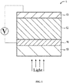
- FIG. 1 Illustration of an organic photovoltaic cell incorporating the polymers of the present invention.
- Organic materials haven been used as semiconductors in organic photovoltaic cells.
- One of the issues with these materials has been that they suffer from low charge carrier mobility (electrical conduction).
- a new semiconductor polymer has been discovered that addresses the drawbacks from current organic materials that are used in photovoltaic cells. These and other non-limiting aspects of the present invention are discussed in further detail in the following sections.
- the semi-conductive polymers of the present invention are based on repeating monomeric units of phthalocyanines.
- the general structure of an substituted phthalocyanines is:
- the incorporation of a group IV metal into a phthalocyanine allows for the production of a monomeric unit that can be used to efficiently produce semi-conductive polymers.
- the group IV metal includes at least two axial bonds that can be coupled to bifunctional spacers to form said monomeric units.
- the following are examples non-limiting monomeric units that can be used in the context of the present invention: wherein, M 1 and M 2 are each independently silicon, germanium, or tin, (R 1 ) n and (R 2 ) n are each independently a hydrocarbon, a hydrogen, or a halogen and n is an integer from 1 to 4, and R 5 and R 6 , are each independently a halogen or a hydroxyl group.
- x is an integer from 1 to 10000
- R 3 is an aryl group or a carbonate group or polymers of said groups
- R 7 is a halogen or a hydroxyl group
- Y 1 and Y 2 are each independently: and R 4 is an aryl group.
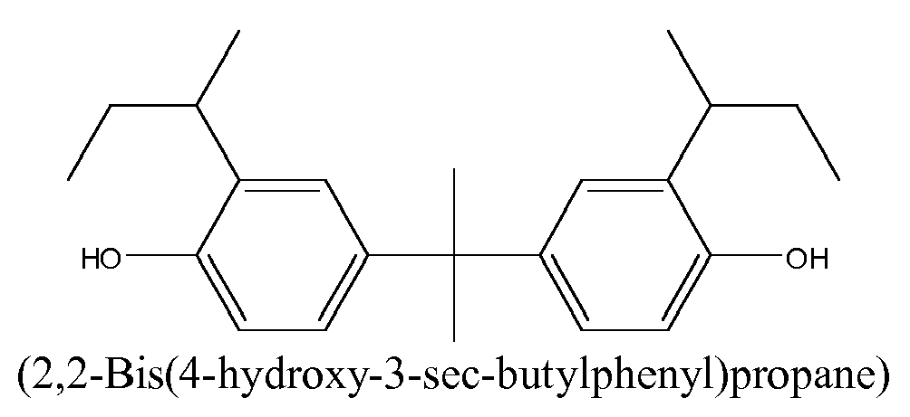
- Non-limiting examples of aryl groups include bisphenols.
- Examples of bisphenols that can be used in the context of the present invention include: or
- FIG. 1 is a cross-sectional view of a non-limiting organic photovoltaic cell that the polymers of the present invention can be incorporated into.
- the organic photovoltaic cell (1) can include a transparent substrate (10), a front electrode (11), a photoactive layer (12), and a back electrode (13). Additional materials, layers, and coatings (not shown) known to those of ordinary skill in the art can be used with photovoltaic cell (1), some of which are described below.
- the organic photovoltaic cell (1) can convert light into usable energy by: (a) photon absorption to produce excitons; (b) exciton diffusion; (c) charge transfer; and (d) charge-transportation to the electrodes.
- the excitons are produced by photon absorption by the photoactive layer (12), which can be a mixture of p-type and n-type organic semiconductor materials ( e.g ., bulk heterojunction) or which can be separate p-type and n-type layers adjacent to one another ( i.e. , bi-layer heterojunction).
- the generated excitons diffuse to the p-n junction.
- the excitons separate into electrons and holes.
- electrons and holes are transported to the electrodes (11) and (13) and are used in a circuit.
- the substrate (10) can be used as support.
- organic photovoltaic cells it is typically transparent or translucent, which allows light to efficiently enter the cell. It is typically made from material that is not easily altered or degraded by heat or organic solvents, and as already noted, has excellent optical transparency.
- Non-limiting examples of such materials include inorganic materials such as alkali-free glass and quartz glass, polymers such as polyethylene, PET, PEN, polyimide, polyamide, polyamidoimide, liquid crystal polymer, and cycloolefin polymer, silicon, and metal.
- the front electrode (11) can be used as a cathode or anode depending on the set-up of the circuit. It is stacked on the substrate (10).
- the front electrode (11) is made of a transparent or translucent conductive material.
- the front electrode (11) is obtained by forming a film using such a material (e.g ., vacuum deposition, sputtering, ion-plating, plating, coating, etc. ).
- transparent or translucent conductive material include metal oxide films, metal films, and conductive polymers.
- Non-limiting examples of metal oxides that can be used to form a film include indium oxide, zinc oxide, tin oxide, and their complexes such as indium stannate (ITO), fluorine-doped tin oxide (FTO), and indium zinc oxide films.
- Non-limiting examples of metals that can be used to form a film include gold, platinum, silver, and copper.
- Non-limiting examples of conductive polymers include polyaniline and polythiophene.
- the thickness of the film for the front electrode (11) is typically between from 30 to 300 nm. If the film thickness is less than 30 nm, then the conductivity can be reduced and the resistance increased, which results in a decrease in photoelectric conversion efficiency.
- the film thickness is greater than 300 nm, then light transmittance may be lowered.
- the sheet resistance of the front electrode (11) is typically 10 ⁇ / ⁇ or less.
- the front electrode (11) may be a single layer or laminated layers formed of materials each having a different work function.
- the back electrode (13) can be used as a cathode or anode depending on the set-up of the circuit. This electrode (13) can be stacked on the photoactive layer (12).
- the material used for the back electrode (13) is conductive. Non-limiting examples of such materials include metals, metal oxides, and conductive polymers ( e.g ., polyaniline, polythiophene, etc. ) such as those discussed above in the context of the front electrode (11).
- the front electrode (11) is formed using a material having high work function
- the back electrode (13) can be made of material having a low work function.
- Non-limiting examples of materials having a low work function include Li, In, Al, Ca, Mg, Sm, Tb, Yb, Zr, Na, K, Rb, Cs, Ba, and the alloys thereof.
- the back electrode (13) can be a single layer or laminated layers formed of materials each having a different work function. Further, it may be an alloy of one or more of the materials having a low work function and at least one selected from the group consisting of gold, silver, platinum, copper, manganese, titanium, cobalt, nickel, tungsten, and tin.
- the alloy examples include a lithium-aluminum alloy, a lithium-magnesium alloy, a lithium-indium alloy, a magnesium-silver alloy, a magnesium-indium alloy, a magnesium-aluminium alloy, an indium-silver alloy, and a calcium-aluminum alloy.
- the film thickness of the back electrode (13) can be from 1 to 1000 nm or from 10 to 500 nm. If the film thickness is too small, then the resistance can be excessively large and the generated charge may not be sufficiently transmitted to the external circuit.
- the front (11) and back (13) electrodes can be further coated with hole transport or electron transport layers (not shown in FIG. 1 ) to increase the efficiency and prevent short circuits of the organic photovoltaic cell (1).
- the hole transport layer and the electron transport layer can be interposed between the electrode and the photoactive layer (12).
- Non-limiting examples of the materials that can be used for the hole transport layer include polythiophene-based polymers such as PEDOT/PSS (poly(3,4-ethylenedioxythiophene)-poly(styrene sulfonate)) and organic conductive polymers such as polyaniline and polypyrrole.
- the film thickness of the hole transport layer can be from 20 to 100 nm.
- the film thickness is too thin, short circuit of the electrode can occur more readily. If the film thickness is too thick, the film resistance is large and the generated electric current could be limited and optical conversion efficiency can be reduced.
- the electron transport layer it can function by blocking holes and transporting electrons more efficiently.
- Non-limiting examples of the type of material that the electron transport layer can be made of include metal oxides (e.g ., amorphous titanium oxide). When titanium oxide is used, the film thickness can range from 5 to 20 nm. If the film thickness is too thin, the hole blocking effect can be reduced and thus the generated excitons are deactivated before the excitons dissociate into electrons and holes. By comparison, when the film thickness is too thick, the film resistance is large, the generated electric current is limited, resulting in reduction of optical conversion efficiency.
- the photoactive layer (12) can be interposed between the front electrode (10) and the back electrode (13).
- the photoactive layer (12) can be a bulk hetero-junction type layer such that the polymers of the present invention are mixed with a second semi-conductive material (e.g ., a second polymer or a small molecule) and a micro phase separation occurs within said layer (12).
- the photoactive layer (12) can be a bi-layer hetero-junction type layer such that the polymers of the present invention form one layer and a second photoactive layer is adjacent thereto.
- the layer (12) will include both p-type and n-type organic semiconductors, thereby allowing for the flow of electrons.
- there can be multiple photoactive layers used for a given photovoltaic cell e.g. , 2, 3, 4, or more).
- the photoactive layer can be deposited by obtaining a solution that includes a solvent and the polymers of the present invention solubilized therein.
- solvents include unsaturated hydrocarbon-based solvents such as toluene, xylene, tetralin, decalin, mesitylene, n-butylbenzene, sec-butylbutylbenzene, and tert-butylbenzene; halogenated aromatic hydrocarbon-based solvents such as chlorobenzene, dichlorobenzene, and trichlorobenzene, halogenated saturated hydrocarbon-based solvents such as carbon tetrachloride, chloroform, dichloromethane, dichloroethane, chlorobutane, bromobutane, chloropentane, chlorohexane, bromohexane, and chlorocyclohexane, and ethers such as tetrahydrofuran and tetrahydropyr
- the solution can be deposited by doctor blade coating, spin coating, meniscus coating, transfer printing, ink jet printing, offset printing, screen printing process, dip coating, casting, bar coating, roll coating, wire bar coating, spraying, screen printing, gravure printing, flexo printing, offset printing, gravure offset printing, dispenser coating, nozzle coating, capillary coating, etc .
- Germanium phthalocyanine (GePc) containing polymers were synthesized in a 25 mL three-neck round bottom glass flask equipped with a condenser, thermal well, and a magnetic Teflon stir bar. The flask was placed inside a heating mantle, and the equipment was placed on a magnetic stirrer. The dichloro germanium phthalocyanine (GePc-Cl 2 ) was sublimed prior to being used.
- Germanium phthalocyanine (GePc) containing polymers were synthesized in a 100 mL three-neck round bottom glass flask equipped with a condenser and a magnetic Teflon stir bar. The dichloro germanium phthalocyanine (GePc-Cl 2 ) was sublimed prior to being used. Prior to sealing the reactor a mixture of GePc-Cl 2 (0.765g, 1.20mmol), 2,2-Bis(4-hydroxy-3-sec-butylphenyl)propane (0.394g, 1.2mmol), potassium phosphate tribasic (K 3 PO 4 , 1.44g, 6.9mmol) and chlorobenzene (10ml) were added.
- GePc-Cl 2 0.765g, 1.20mmol
- 2,2-Bis(4-hydroxy-3-sec-butylphenyl)propane 0.394g, 1.2mmol
- potassium phosphate tribasic K 3 PO 4 , 1.44g, 6.9mmol
- the reactor was then heated to the appropriate temperature 120 °C while maintaining a nitrogen purge.
- the polymerization was stopped after 40 hours and then cooled to room temperature, which resulted in a crude polymer.
- the crude polymer was precipitated into methanol, filtered and dried in a vacuum oven overnight.
- Silicon phthalocyanine (SiPc) containing polymers were synthesized in a 100 mL three-neck round bottom glass flask equipped with a condenser and a magnetic Teflon stir bar.
- the dichloro germanium phthalocyanine (SiPc-Cl 2 ) was sublimed prior to being used.
- a mixture of SiPc-Cl 2 0.80g, 1.20mmol
- 2,2-Bis(4-hydroxy-3-sec-butylphenyl)propane 0.394g, 1.2mmol
- potassium phosphate tribasic K 3 PO 4 , 1.44g, 6.9mmol
- chlorobenzene (10ml) were added.
- the reactor was then heated to the appropriate temperature 120 °C while maintaining a nitrogen purge.
- the polymerization was stopped after 40 hours and then cooled to room temperature, which resulted in a crude polymer.
- the crude polymer was precipitated into methanol, filtered and dried in a vacuum oven overnight.
- Silicon phthalocyanine (SiPc) containing polymers were synthesized in a 250 mL three-neck round bottom glass flask equipped with a condenser and a magnetic Teflon stir bar.
- the dichloro germanium phthalocyanine (SiPc-Cl 2 ) was sublimed prior to being used.
- a mixture of SiPc-Cl 2 0.80g, 1.07mmol
- 2,2-Bis(4-hydroxy-3-sec-butylphenyl)propane 0.182g, 0.54mmol
- m-bisphenol 0.186g, 0.53mmol
- potassium carbonate K 2 CO 3 , 0.59g, 4.3mmol
- chlorobenzene (20ml) were added.
- the reactor was then heated to the appropriate temperature 120 °C while maintaining a nitrogen purge.
- the polymerization was stopped after 40 hours and then cooled to room temperature, which resulted in a crude polymer.
- the crude polymer was precipitated into methanol, filtered and dried in a vacuum oven overnight.
Landscapes
- Chemical & Material Sciences (AREA)
- Engineering & Computer Science (AREA)
- Materials Engineering (AREA)
- Inorganic Chemistry (AREA)
- Organic Chemistry (AREA)
- Physics & Mathematics (AREA)
- High Energy & Nuclear Physics (AREA)
- Photovoltaic Devices (AREA)
- Addition Polymer Or Copolymer, Post-Treatments, Or Chemical Modifications (AREA)
- Bipolar Transistors (AREA)
- Polyoxymethylene Polymers And Polymers With Carbon-To-Carbon Bonds (AREA)
Description
- This application claims the benefit of
U.S. Provisional Application No. 61/777,452, filed March 12, 2013 - The invention generally concerns the use of semi-conductive polymers that can be used in organic photovoltaic cells.
- Rising energy prices and concerns relating to global warming from burning fossil fuels has led to a search for more cost effective and efficient renewable energy sources. One such source of renewable energy that has been identified is solar energy. The problems associated with converting solar energy into electricity has been, in large part due to the inefficiencies of the energy conversion process. For instance, photovoltaic cells (e.g., solar cells) have been developed that can convert solar energy into usable energy, but the costs associated with doing so have hindered the widespread application of this technology into the marketplace.
- In recent years research relating to the use of polymers in the photoactive layers of organic photovoltaic cells has increased. One of the unique aspects of using polymers is that they allow organic electronic devices to be manufactured by cost-effective solution-processing techniques such as spin casting, dip coating or ink jet printing. Solution processing can be carried out cheaper and on a larger scale compared to the evaporative techniques used to make inorganic thin film devices, which rely on vacuum deposition techniques. Many of the polymers that are currently being used suffer from low charge carrier mobility (electrical conduction) and are complicated to synthesize, which increases the ultimate costs of production.
-
US 4 622 170 A pertains to electrically conductive cofacially crystallizing organomacrocycle forming compositions, and discloses methods and formable compositions for fabricating electrically conductive articles comprising cofacially stacking organomacrocycles and as cofacially stacking phthalocyanines, in which a composition comprising a cofacially stacking phthalocyanine in strong Bronsted acid is formed into a desired shape such as a fiber or film, solidified by removal of the solvent, and provided in fractional valence state. -
US 4 839 112 A refers to methods for fabricating a low dimensionally electroconductive article. In particular, this document discloses methods for fabricating low dimensionally electroconductive articles comprising cofacially stacking organomacrocycles and as cofacially stacking phthalocyanines, in which a composition comprising a cofacially stacking phthalocyanine in strong Bronsted acid is formed into a desired shape such as a fiber or film, solidified by removal of the solvent, and provided in fractional valence state. - According to an aspect, there is provided a polymer having a structure of:

- M1 and M2 are each independently silicon, germanium, or tin;
- (R1)n and (R2)n are each independently a hydrocarbon, a hydrogen, or a halogen and n is an integer from 1 to 4;
- R3 is an aryl group or a carbonate group; and
- x is an integer from 1 to 1000.
- According to a further aspect, there is provided a photovoltaic cell comprising photoactive layer comprising a polymer having a structure of:

- M1 and M2 are each independently silicon, germanium, or tin;
- (R1)n and (R2)n are each independently a hydrocarbon, a hydrogen, or a halogen and n is an integer from 1 to 4;
- R3 is an aryl group or a carbonate group; and
- x is an integer from 1 to 1000.
- According to a further aspect, there is provided a solution comprising a polymer having a structure of:

- M1 and M2 are each independently silicon, germanium, or tin;
- (R1)n and (R2)n are each independently a hydrocarbon, a hydrogen, or a halogen and n is an integer from 1 to 4;
- R3 is an aryl group or a carbonate group; and
- x is an integer from 1 to 1000,
- According to a further aspect, there is provided a process for making a photoactive layer on a substrate, wherein the photoactive layer comprises a polymer
having a structure of:
- M1 and M2 are each independently silicon, germanium, or tin;
- (R1)n and (R2)n are each independently a hydrocarbon, a hydrogen, or a halogen and n is an integer from 1 to 4;
- R3 is an aryl group or a carbonate group; and
- x is an integer from 1 to 1000,
- M1 and M2 are each independently silicon, germanium, or tin;
- (R1)n and (R2)n are each independently a hydrocarbon, a hydrogen, or a halogen and n is an integer from 1 to 4;
- R3 is an aryl group or a carbonate group; and
- x is an integer from 1 to 1000,
- It has been discovered that polymers made from phthalocyanines (nPcs) containing group IV metals have semi-conductive properties and can be used in the photoactive layer of an organic photovoltaic cell. The group IV metal (i.e., silicon, germanium, and tin) containing Pcs include at least two axial bonds that can be coupled to bifunctional spacers. This results in building blocks that can be used to form the polymers of the present invention (e.g., though a condensation reaction).
- In at least one aspect of the present invention there is disclosed a polymer that can be used in a photoactive layer in an organic photovoltaic cell having a structure of:


- Also disclosed is an organic photovoltaic cell that includes a photoactive layer or layers. The photoactive layer or layers can include any one of the polymers of the present invention. The photovoltaic cell can include a transparent or translucent substrate, a transparent or translucent electrode, the photoactive layer or layers, and a second electrode, wherein the photoactive layer or layer is disposed between the transparent/translucent electrode and the second electrode. The transparent/translucent electrode can be a cathode and the second electrode can be an anode or the transparent/translucent electrode can be an anode and the second electrode can be a cathode. In certain instances, the second electrode is opaque/not-transparent. The photovoltaic cell can be a bulk heterojunction photovoltaic cell or a bi-layer photovoltaic cell for example.
- In another embodiment, there is disclosed an organic electronic device that includes any one of the photovoltaic cells or polymers of the present invention. Non-limiting examples of organic electronic devices include polymeric organic light-emitting diodes (PLEDs), organic integrated circuits (O-ICs), organic field effect transistors (OFETs), organic thin film transistors (OTFTs), organic solar cells (O-SCs) or organic laser diodes (O-lasers).
- In still another aspect of the present invention there is disclosed a solution comprising any one of the polymers of the invention dissolved in said solution. The solvent used can be one that effectively solubilizes the polymer. Non-limiting examples of solvents include toluene, xylene, tetralin, decalin, mesitylene, n-butylbenzene, sec-butylbutylbenzene, and tert-butylbenzene; halogenated aromatic hydrocarbon-based solvents such as chlorobenzene, dichlorobenzene, and trichlorobenzene, halogenated saturated hydrocarbon-based solvents such as carbon tetrachloride, chloroform, dichloromethane, dichloroethane, chlorobutane, bromobutane, chloropentane, chlorohexane, bromohexane, and chlorocyclohexane, and ethers such as tetrahydrofuran and tetrahydropyran. The solution can be deposited by doctor blade coating, spin coating, meniscus coating, transfer printing, ink jet printing, offset printing, screen printing process, dip coating, casting, bar coating, roll coating, wire bar coating, spraying, screen printing, gravure printing, flexo printing, offset printing, gravure offset printing, dispenser coating, nozzle coating, capillary coating, etc.
- Also disclosed are the following
Embodiments 1 to 39 of the present invention.Embodiment 1 is a polymer having a structure of:
Embodiment 1, wherein at least one of M1 and M2 are germanium or tin. Embodiment 3 is the polymer of Embodiment 2, wherein M1 is silicon and M2 is germanium. Embodiment 4 is the polymer ofEmbodiment 1, wherein the aryl group includes 6 to 84 carbon atoms, or 6 to 24 carbon atoms, or 6 to 18 carbon atoms. Embodiment 5 is the polymer of Embodiment 4, wherein the R3 aryl group includes a non-carbon ring atom, wherein the non-carbon ring atom is a halogen, oxygen, sulfur or nitrogen. Embodiment 6 is the polymer of any one ofEmbodiments 1 to 5, wherein the R3 aryl group is a bisphenol. Embodiment 7 is the polymer of Embodiment 6, wherein the bisphenol is m-(C6H4)-C(CH3)2-C6H4-C(CH3)2-m-(C6H4)-. Embodiment 8 is the polymer of any one ofEmbodiments 1 to 7, wherein (R1)n is a substituted or un-substituted hydrocarbon. Embodiment 9 is the polymer of Embodiment 8, wherein the hydrocarbon is a methyl, ethyl, propyl, isopropyl, n-butyl, sec-butyl or tert-butyl group.Embodiment 10 is the polymer of any one ofEmbodiments 1 to 7, wherein (R1)n is a halogen and n is 1.Embodiment 11 is the polymer ofEmbodiment 10, wherein the halogen is F, Cl, Br, orI. Embodiment 12 is the polymer of any one ofEmbodiments 1 to 7, wherein (R1)n is a hydrogen and n is 1.Embodiment 13 is the polymer of any one of Embodiments 8 to 12, wherein (R2)n is a substituted or un-substituted hydrocarbon. Embodiment 14 is the polymer ofEmbodiment 13, wherein the hydrocarbon is a methyl, ethyl, propyl, isopropyl, n-butyl, sec-butyl or tert-butyl group. Embodiment 15 is the polymer of any one of Embodiments 8 to 12, wherein (R2)n is a halogen and n is 1. Embodiment 16 is the polymer of Embodiment 15, wherein the halogen is F, Cl, Br, or I. Embodiment 17 is the polymer of any one of Embodiments 8 to 12, wherein (R2)n is a hydrogen and n is 1. Embodiment 18 is the polymer of any one ofEmbodiments 1 to 17, wherein the polymer has the following structure:

Embodiments 1 to 22, wherein the polymer is the reaction product of
Embodiments 1 to 25, wherein the polymer is a semi-conductive polymer. Embodiment 27 is the polymer of Embodiment 26, wherein the polymer is modified with a dopant so as to enhance its p-type or n-type properties. Embodiment 28 is a photovoltaic cell comprising photoactive layer comprising a polymer of any one ofEmbodiments 1 to 27. Embodiment 29 is the photovoltaic cell of Embodiment 28, comprising a transparent substrate, a transparent electrode, the photoactive layer, and a second electrode, wherein the photoactive layer is disposed between the transparent electrode and the second electrode. Embodiment 30 is the photovoltaic cell of Embodiment 29, wherein the transparent electrode is a cathode and the second electrode is an anode. Embodiment 31 is the photovoltaic cell of Embodiment 29, wherein the transparent electrode is an anode and the second electrode is a cathode. Embodiment 32 is the photovoltaic cell of any one Embodiments 28 to 31, wherein the second electrode is not transparent. Embodiment 33 is the photovoltaic cell of any one of Embodiments 28 to 32, wherein photovoltaic cell is a bulk heterojunction photovoltaic cell. Embodiment 34 is the photovoltaic cell of any one of Embodiments 28 to 32, wherein photovoltaic cell is a bi-layer photovoltaic cell. Embodiment 35 is the photovoltaic cell of any one of Embodiments 28 to 34, wherein the photovoltaic cell is comprised in an organic electronic device. Embodiment 36 is the photovoltaic cell of Embodiment 35, wherein the organic electronic device is a polymeric organic light-emitting diode (PLED), an organic integrated circuit (O-IC), an organic field effect transistor (OFET), an organic thin film transistor (OTFT), an organic solar cell (O-SC) or an organic laser diode (O-laser). Embodiment 37 is a solution comprising any one of the polymers ofEmbodiments 1 to 27, wherein the polymer is dissolved in said solution. Embodiment 38 is a process for making a photoactive layer on a substrate, wherein the photoactive layer comprises any one of the polymers ofEmbodiments 1 to 27, the process comprising disposing the solution of Embodiment 36 on the substrate and drying said solution to form the photoactive layer. Embodiment 39 is the process of Embodiment 38, wherein the solution is disposed on the substrate layer by a doctor blade coating, spin coating, meniscus coating, transfer printing, ink jet printing, offset printing or screen printing process. - The term "about" or "approximately" are defined as being close to as understood by one of ordinary skill in the art, and in one non-limiting embodiment the terms are defined to be within 10%, preferably within 5%, more preferably within 1%, and most preferably within 0.5%.
- Other objects, features and advantages of the present invention will become apparent from the following figures, detailed description, and examples. It should be understood, however, that the figures, detailed description, and examples, while indicating specific embodiments of the invention, are given by way of illustration only and are not meant to be limiting.
-
FIG. 1 : Illustration of an organic photovoltaic cell incorporating the polymers of the present invention. - Organic materials haven been used as semiconductors in organic photovoltaic cells. One of the issues with these materials has been that they suffer from low charge carrier mobility (electrical conduction).
- A new semiconductor polymer has been discovered that addresses the drawbacks from current organic materials that are used in photovoltaic cells. These and other non-limiting aspects of the present invention are discussed in further detail in the following sections.
- The semi-conductive polymers of the present invention are based on repeating monomeric units of phthalocyanines. The general structure of an substituted phthalocyanines is:

- As noted above, the incorporation of a group IV metal into a phthalocyanine allows for the production of a monomeric unit that can be used to efficiently produce semi-conductive polymers. In particular, the group IV metal includes at least two axial bonds that can be coupled to bifunctional spacers to form said monomeric units. The following are examples non-limiting monomeric units that can be used in the context of the present invention:


- The following is a reaction scheme that can be used to prepare the semi-conductive polymers of the present invention:


- Non-limiting examples of aryl groups include bisphenols. Examples of bisphenols that can be used in the context of the present invention include:




- The semi-conductive polymers of the present invention can be used in organic photovoltaic cells.
FIG. 1 is a cross-sectional view of a non-limiting organic photovoltaic cell that the polymers of the present invention can be incorporated into. The organic photovoltaic cell (1) can include a transparent substrate (10), a front electrode (11), a photoactive layer (12), and a back electrode (13). Additional materials, layers, and coatings (not shown) known to those of ordinary skill in the art can be used with photovoltaic cell (1), some of which are described below. - Generally speaking, the organic photovoltaic cell (1) can convert light into usable energy by: (a) photon absorption to produce excitons; (b) exciton diffusion; (c) charge transfer; and (d) charge-transportation to the electrodes. With respect to (a), the excitons are produced by photon absorption by the photoactive layer (12), which can be a mixture of p-type and n-type organic semiconductor materials (e.g., bulk heterojunction) or which can be separate p-type and n-type layers adjacent to one another (i.e., bi-layer heterojunction). For (b), the generated excitons diffuse to the p-n junction. Then in (c), the excitons separate into electrons and holes. For (d), electrons and holes are transported to the electrodes (11) and (13) and are used in a circuit.
- The substrate (10) can be used as support. For organic photovoltaic cells, it is typically transparent or translucent, which allows light to efficiently enter the cell. It is typically made from material that is not easily altered or degraded by heat or organic solvents, and as already noted, has excellent optical transparency. Non-limiting examples of such materials include inorganic materials such as alkali-free glass and quartz glass, polymers such as polyethylene, PET, PEN, polyimide, polyamide, polyamidoimide, liquid crystal polymer, and cycloolefin polymer, silicon, and metal.
- The front electrode (11) can be used as a cathode or anode depending on the set-up of the circuit. It is stacked on the substrate (10). The front electrode (11) is made of a transparent or translucent conductive material. Typically, the front electrode (11) is obtained by forming a film using such a material (e.g., vacuum deposition, sputtering, ion-plating, plating, coating, etc.). Non-limiting examples of transparent or translucent conductive material include metal oxide films, metal films, and conductive polymers. Non-limiting examples of metal oxides that can be used to form a film include indium oxide, zinc oxide, tin oxide, and their complexes such as indium stannate (ITO), fluorine-doped tin oxide (FTO), and indium zinc oxide films. Non-limiting examples of metals that can be used to form a film include gold, platinum, silver, and copper. Non-limiting examples of conductive polymers include polyaniline and polythiophene. The thickness of the film for the front electrode (11) is typically between from 30 to 300 nm. If the film thickness is less than 30 nm, then the conductivity can be reduced and the resistance increased, which results in a decrease in photoelectric conversion efficiency. If the film thickness is greater than 300 nm, then light transmittance may be lowered. Also, the sheet resistance of the front electrode (11) is typically 10Ω/□ or less. Further, the front electrode (11) may be a single layer or laminated layers formed of materials each having a different work function.
- The back electrode (13) can be used as a cathode or anode depending on the set-up of the circuit. This electrode (13) can be stacked on the photoactive layer (12). The material used for the back electrode (13) is conductive. Non-limiting examples of such materials include metals, metal oxides, and conductive polymers (
e.g ., polyaniline, polythiophene, etc.) such as those discussed above in the context of the front electrode (11). When the front electrode (11) is formed using a material having high work function, then the back electrode (13) can be made of material having a low work function. Non-limiting examples of materials having a low work function include Li, In, Al, Ca, Mg, Sm, Tb, Yb, Zr, Na, K, Rb, Cs, Ba, and the alloys thereof. The back electrode (13) can be a single layer or laminated layers formed of materials each having a different work function. Further, it may be an alloy of one or more of the materials having a low work function and at least one selected from the group consisting of gold, silver, platinum, copper, manganese, titanium, cobalt, nickel, tungsten, and tin. Examples of the alloy include a lithium-aluminum alloy, a lithium-magnesium alloy, a lithium-indium alloy, a magnesium-silver alloy, a magnesium-indium alloy, a magnesium-aluminium alloy, an indium-silver alloy, and a calcium-aluminum alloy. The film thickness of the back electrode (13) can be from 1 to 1000 nm or from 10 to 500 nm. If the film thickness is too small, then the resistance can be excessively large and the generated charge may not be sufficiently transmitted to the external circuit. - In some embodiments, the front (11) and back (13) electrodes can be further coated with hole transport or electron transport layers (not shown in
FIG. 1 ) to increase the efficiency and prevent short circuits of the organic photovoltaic cell (1). The hole transport layer and the electron transport layer can be interposed between the electrode and the photoactive layer (12). Non-limiting examples of the materials that can be used for the hole transport layer include polythiophene-based polymers such as PEDOT/PSS (poly(3,4-ethylenedioxythiophene)-poly(styrene sulfonate)) and organic conductive polymers such as polyaniline and polypyrrole. The film thickness of the hole transport layer can be from 20 to 100 nm. If the film thickness is too thin, short circuit of the electrode can occur more readily. If the film thickness is too thick, the film resistance is large and the generated electric current could be limited and optical conversion efficiency can be reduced. As for the electron transport layer, it can function by blocking holes and transporting electrons more efficiently. Non-limiting examples of the type of material that the electron transport layer can be made of include metal oxides (e.g., amorphous titanium oxide). When titanium oxide is used, the film thickness can range from 5 to 20 nm. If the film thickness is too thin, the hole blocking effect can be reduced and thus the generated excitons are deactivated before the excitons dissociate into electrons and holes. By comparison, when the film thickness is too thick, the film resistance is large, the generated electric current is limited, resulting in reduction of optical conversion efficiency. - The photoactive layer (12) can be interposed between the front electrode (10) and the back electrode (13). In one instance, the photoactive layer (12) can be a bulk hetero-junction type layer such that the polymers of the present invention are mixed with a second semi-conductive material (e.g., a second polymer or a small molecule) and a micro phase separation occurs within said layer (12). Alternatively, the photoactive layer (12) can be a bi-layer hetero-junction type layer such that the polymers of the present invention form one layer and a second photoactive layer is adjacent thereto. In either instance, the layer (12) will include both p-type and n-type organic semiconductors, thereby allowing for the flow of electrons. Further, there can be multiple photoactive layers used for a given photovoltaic cell (e.g., 2, 3, 4, or more).
- The photoactive layer can be deposited by obtaining a solution that includes a solvent and the polymers of the present invention solubilized therein. Non-limiting examples of such solvents include unsaturated hydrocarbon-based solvents such as toluene, xylene, tetralin, decalin, mesitylene, n-butylbenzene, sec-butylbutylbenzene, and tert-butylbenzene; halogenated aromatic hydrocarbon-based solvents such as chlorobenzene, dichlorobenzene, and trichlorobenzene, halogenated saturated hydrocarbon-based solvents such as carbon tetrachloride, chloroform, dichloromethane, dichloroethane, chlorobutane, bromobutane, chloropentane, chlorohexane, bromohexane, and chlorocyclohexane, and ethers such as tetrahydrofuran and tetrahydropyran. The solution can be deposited by doctor blade coating, spin coating, meniscus coating, transfer printing, ink jet printing, offset printing, screen printing process, dip coating, casting, bar coating, roll coating, wire bar coating, spraying, screen printing, gravure printing, flexo printing, offset printing, gravure offset printing, dispenser coating, nozzle coating, capillary coating, etc.
- The present invention will be described in greater detail by way of specific examples. The following examples are offered for illustrative purposes only, and are not intended to limit the invention in any manner. Those of skill in the art will readily recognize a variety of noncritical parameters which can be changed or modified to yield essentially the same results.
- Germanium phthalocyanine (GePc) containing polymers were synthesized in a 25 mL three-neck round bottom glass flask equipped with a condenser, thermal well, and a magnetic Teflon stir bar. The flask was placed inside a heating mantle, and the equipment was placed on a magnetic stirrer. The dichloro germanium phthalocyanine (GePc-Cl2) was sublimed prior to being used. Prior to sealing the reactor a mixture of GePc-Cl2 (100mg, 0.15mmol), m-bisphenol (50mg, 0.144mmol) and 4-tertbutylpheonol (2.2mg, 0.0152mmol) and chlorobenzene (5ml) were added. The polymerization target number-average molecular weight (Mn) at complete conversion was calculated to equal 20 kg mol-1. Once sealed the mixture was bubbled with nitrogen and for 20 minutes prior to heating. The reactor was then heated to the appropriate temperature 120 °C while maintaining a nitrogen purge. The polymerization was stopped after 40 hours and then cooled to room temperature, which resulted in a crude polymer. The crude polymer was precipitated into methanol, filtered and dried in a vacuum oven overnight.
- Germanium phthalocyanine (GePc) containing polymers were synthesized in a 100 mL three-neck round bottom glass flask equipped with a condenser and a magnetic Teflon stir bar. The dichloro germanium phthalocyanine (GePc-Cl2) was sublimed prior to being used. Prior to sealing the reactor a mixture of GePc-Cl2 (0.765g, 1.20mmol), 2,2-Bis(4-hydroxy-3-sec-butylphenyl)propane (0.394g, 1.2mmol), potassium phosphate tribasic (K3PO4, 1.44g, 6.9mmol) and chlorobenzene (10ml) were added. The reactor was then heated to the appropriate temperature 120 °C while maintaining a nitrogen purge. The polymerization was stopped after 40 hours and then cooled to room temperature, which resulted in a crude polymer. The crude polymer was precipitated into methanol, filtered and dried in a vacuum oven overnight.
- Silicon phthalocyanine (SiPc) containing polymers were synthesized in a 100 mL three-neck round bottom glass flask equipped with a condenser and a magnetic Teflon stir bar. The dichloro germanium phthalocyanine (SiPc-Cl2) was sublimed prior to being used. Prior to sealing the reactor a mixture of SiPc-Cl2 (0.680g, 1.20mmol), 2,2-Bis(4-hydroxy-3-sec-butylphenyl)propane (0.394g, 1.2mmol), potassium phosphate tribasic (K3PO4, 1.44g, 6.9mmol) and chlorobenzene (10ml) were added. The reactor was then heated to the appropriate temperature 120 °C while maintaining a nitrogen purge. The polymerization was stopped after 40 hours and then cooled to room temperature, which resulted in a crude polymer. The crude polymer was precipitated into methanol, filtered and dried in a vacuum oven overnight.
- Silicon phthalocyanine (SiPc) containing polymers were synthesized in a 250 mL three-neck round bottom glass flask equipped with a condenser and a magnetic Teflon stir bar. The dichloro germanium phthalocyanine (SiPc-Cl2) was sublimed prior to being used. Prior to sealing the reactor a mixture of SiPc-Cl2 (0.680g, 1.07mmol), 2,2-Bis(4-hydroxy-3-sec-butylphenyl)propane (0.182g, 0.54mmol), m-bisphenol (0.186g, 0.53mmol), potassium carbonate (K2CO3, 0.59g, 4.3mmol) and chlorobenzene (20ml) were added. The reactor was then heated to the appropriate temperature 120 °C while maintaining a nitrogen purge. The polymerization was stopped after 40 hours and then cooled to room temperature, which resulted in a crude polymer. The crude polymer was precipitated into methanol, filtered and dried in a vacuum oven overnight.

Claims (20)
- A polymer having a structure of:
 M1 and M2 are each independently silicon, germanium, or tin;(R1)n and (R2)n are each independently a hydrocarbon, a hydrogen, or a halogen and n is an integer from 1 to 4;R3 is an aryl group or a carbonate group; andx is an integer from 1 to 1000.
 - The polymer of claim 1, wherein at least one of M1 and M2 are germanium or tin, optionally wherein M1 is silicon and M2 is germanium.
- The polymer of claim 1, wherein the aryl group includes 6 to 84 carbon atoms, or 6 to 24 carbon atoms, or 6 to 18 carbon atoms, optionally wherein the R3 aryl group includes a non-carbon ring atom, wherein the non-carbon ring atom is a halogen, oxygen, sulfur or nitrogen.
- The polymer of any one of claims 1 to 3, wherein the R3 aryl group is a bisphenol, optionally wherein the bisphenol is m-(C6H4)-C(CH3)2-C6H4-C(CH3)2-m-(C6H4)-.
- The polymer of any one of claims 1 to 4, wherein (R1)n is a substituted or un-substituted hydrocarbon, optionally wherein the hydrocarbon is a methyl, ethyl, propyl, isopropyl, n-butyl, sec-butyl or tert-butyl group.
- The polymer of any one of claims 1 to 5, wherein (R1)n is a halogen and n is 1, optionally wherein the halogen is F, Cl, Br, or I.
- The polymer of any one of claims 1 to 6, wherein (R1)n is a hydrogen and n is 1.
- The polymer of any one of claims 5 to 7, wherein (R2)n is a substituted or un-substituted hydrocarbon. optionally wherein the hydrocarbon is a methyl, ethyl, propyl, isopropyl, n-butyl, sec-butyl or tert-butyl group.
- The polymer of any one of claims 5 to 7, wherein (R2)n is a halogen and n is 1, optionally wherein the halogen is F, Cl, Br, or I.
- The polymer of any one of claims 5 to 7, wherein (R2)n is a hydrogen and n is 1.
- The polymer of any one of claims 1 to 10, wherein the polymer has the following structure:

Y1 and Y2 are each independently
- The polymer of claim 11, wherein the R4 aryl group includes 6 to 22 carbon atoms, or 6 to 18 carbon atoms, or 6 to 10 carbon atoms.
- The polymer of claim 12, wherein the R4 aryl group includes a non-carbon ring atom, wherein the non-carbon ring atom is a halogen, oxygen, sulfur or nitrogen, or wherein the R4 aryl group is p-(C6H4)-C(CH3)3.
- The polymer of claim 11, wherein:M1 is germanium,M2 is silicon,R1 and R2 are each H and n is 1,R3 is m-(C6H4)-C(CH3)2-C6H4-C(CH3)2-m-(C6H4)- andR4 is p-(C6H4)-C(CH3)3.
- The polymer of any one of claims 1 to 14, wherein the polymer is the reaction product of

R5, R6, and R7 are each independently a halogen or a hydroxyl group. - The polymer of claim 15, wherein:M1 and M2 are each silicon,R1 and R2 are each H and n is 1,R3 is C6H4,R4 is C6H5, andR5 and R6, are each a hydroxyl group, andR7 is Cl, or wherein:M1 and M2 are each germanium,R1 and R2 are each H and n is 1,R3 is C6H4,R4 is C6H5, andR5 and R6, are each a hydroxyl group, andR7 is a hydroxyl group.
- The polymer of any one of claims 1 to 16, wherein the polymer is a semi-conductive polymer, and optionally wherein the polymer is modified with a dopant so as to enhance its p-type or n-type properties.
- A photovoltaic cell comprising photoactive layer comprising a polymer of any one of claims 1 to 17.
- A solution comprising any one of the polymers of claims 1 to 17, wherein the polymer is dissolved in said solution.
- A process for making a photoactive layer on a substrate, wherein the photoactive layer comprises any one of the polymers of claims 1 to 17, the process comprising disposing the solution of claim 19 on the substrate and drying said solution to form the photoactive layer, and optionally wherein the solution is disposed on the substrate layer by a doctor blade coating, spin coating, meniscus coating, transfer printing, ink jet printing, offset printing or screen printing process.
Applications Claiming Priority (2)
| Application Number | Priority Date | Filing Date | Title |
|---|---|---|---|
| US201361777452P | 2013-03-12 | 2013-03-12 | |
| PCT/IB2014/001021 WO2014140859A2 (en) | 2013-03-12 | 2014-03-06 | Semiconductor polymers |
Publications (2)
| Publication Number | Publication Date |
|---|---|
| EP2970570A2 EP2970570A2 (en) | 2016-01-20 |
| EP2970570B1 true EP2970570B1 (en) | 2017-04-19 |
Family
ID=51212884
Family Applications (1)
| Application Number | Title | Priority Date | Filing Date |
|---|---|---|---|
| EP14741940.2A Not-in-force EP2970570B1 (en) | 2013-03-12 | 2014-03-06 | Semiconductor polymers |
Country Status (6)
| Country | Link |
|---|---|
| US (1) | US9343688B2 (en) |
| EP (1) | EP2970570B1 (en) |
| KR (1) | KR101714949B1 (en) |
| CN (1) | CN105026457B (en) |
| TW (1) | TWI575027B (en) |
| WO (1) | WO2014140859A2 (en) |
Families Citing this family (1)
| Publication number | Priority date | Publication date | Assignee | Title |
|---|---|---|---|---|
| CN112159519B (en) * | 2020-09-24 | 2021-07-06 | 中国科学院长春光学精密机械与物理研究所 | A kind of porous polyphthalocyanine laser protection material with carbon bridge and preparation method thereof |
Family Cites Families (4)
| Publication number | Priority date | Publication date | Assignee | Title |
|---|---|---|---|---|
| US4622170A (en) | 1982-12-20 | 1986-11-11 | Northwestern University | Electrically conductive cofacially crystallizing organomacrocycle forming compositions |
| US4839112A (en) * | 1982-12-20 | 1989-06-13 | Northwestern University | Methods for fabricating a low dimensionally electroconductive article |
| US8471020B2 (en) | 2011-03-03 | 2013-06-25 | Basf Se | Perylene-based semiconducting materials |
| JP5300903B2 (en) | 2011-03-29 | 2013-09-25 | 株式会社東芝 | Polymer, solar cell and solar power generation system using the same |
-
2014
- 2014-03-06 EP EP14741940.2A patent/EP2970570B1/en not_active Not-in-force
- 2014-03-06 KR KR1020157026387A patent/KR101714949B1/en not_active Expired - Fee Related
- 2014-03-06 CN CN201480011733.3A patent/CN105026457B/en not_active Expired - Fee Related
- 2014-03-06 US US14/199,380 patent/US9343688B2/en not_active Expired - Fee Related
- 2014-03-06 WO PCT/IB2014/001021 patent/WO2014140859A2/en not_active Ceased
- 2014-03-12 TW TW103108793A patent/TWI575027B/en not_active IP Right Cessation
Non-Patent Citations (1)
| Title |
|---|
| None * |
Also Published As
| Publication number | Publication date |
|---|---|
| KR101714949B1 (en) | 2017-03-09 |
| WO2014140859A3 (en) | 2015-02-19 |
| CN105026457B (en) | 2017-03-29 |
| US9343688B2 (en) | 2016-05-17 |
| TW201500476A (en) | 2015-01-01 |
| WO2014140859A2 (en) | 2014-09-18 |
| CN105026457A (en) | 2015-11-04 |
| US20140272158A1 (en) | 2014-09-18 |
| TWI575027B (en) | 2017-03-21 |
| KR20150131069A (en) | 2015-11-24 |
| EP2970570A2 (en) | 2016-01-20 |
Similar Documents
| Publication | Publication Date | Title |
|---|---|---|
| JP5300903B2 (en) | Polymer, solar cell and solar power generation system using the same | |
| EP2067806A1 (en) | Organic photoelectric conversion device and polymer useful for producing the same | |
| JP2012522067A (en) | Carbazole-containing conductive polymer and organic photovoltaic device using the same | |
| JP2015191965A (en) | Photoelectric conversion element, method of manufacturing the same, solar cell, and solar cell module | |
| JP2017515945A (en) | Crystallization of additives at P / N junctions in bulk heterojunction photoactive layers | |
| Liu et al. | A rational design and synthesis of cross-conjugated small molecule acceptors approaching high-performance fullerene-free polymer solar cells | |
| JP6115885B2 (en) | Photoelectric conversion element, solar cell, and solar cell module | |
| Kuznetsov et al. | Thiazolothiazole-based conjugated polymers for blade-coated organic solar cells processed from an environment-friendly solvent | |
| JP2008106239A (en) | Organic photoelectric conversion element and polymer useful for producing the same | |
| JP5476660B2 (en) | Organic photoelectric conversion device and polymer useful for production thereof | |
| US9444060B2 (en) | Synthesis of new small molecules/oligomers with high conductivity and absorption for optoelectronic application | |
| US9343688B2 (en) | Semiconductor polymers | |
| JP2014189666A (en) | Composition for forming semiconductor layer and solar cell element using the composition | |
| US9472771B2 (en) | Method of making axially fluorinated-phthalocyanines with an aprotic fluoride compound | |
| JP6068729B2 (en) | Compounds with electron-rich and electron-deficient sites and their use in organic electronic applications | |
| JP6143151B2 (en) | Photoelectric conversion element, solar cell and solar cell module | |
| WO2011148900A1 (en) | Polymer compound and photoelectric conversion element using the same | |
| JP6733455B2 (en) | Photoelectric conversion element, solar cell and solar cell module | |
| WO2013183548A1 (en) | Organic photoelectric conversion element fabrication method | |
| JP2016066645A (en) | Photoelectric conversion element and manufacturing method for photoelectric conversion element | |
| JP2016184698A (en) | Photoelectric transducer, solar cell, and solar cell module |
Legal Events
| Date | Code | Title | Description |
|---|---|---|---|
| PUAI | Public reference made under article 153(3) epc to a published international application that has entered the european phase |
Free format text: ORIGINAL CODE: 0009012 |
|
| 17P | Request for examination filed |
Effective date: 20150819 |
|
| AK | Designated contracting states |
Kind code of ref document: A2 Designated state(s): AL AT BE BG CH CY CZ DE DK EE ES FI FR GB GR HR HU IE IS IT LI LT LU LV MC MK MT NL NO PL PT RO RS SE SI SK SM TR |
|
| AX | Request for extension of the european patent |
Extension state: BA ME |
|
| RIN1 | Information on inventor provided before grant (corrected) |
Inventor name: BENDER, TIMOTHY, P. Inventor name: LESSARD, BENOIT, H. |
|
| DAX | Request for extension of the european patent (deleted) | ||
| 17Q | First examination report despatched |
Effective date: 20160803 |
|
| GRAP | Despatch of communication of intention to grant a patent |
Free format text: ORIGINAL CODE: EPIDOSNIGR1 |
|
| INTG | Intention to grant announced |
Effective date: 20161123 |
|
| GRAS | Grant fee paid |
Free format text: ORIGINAL CODE: EPIDOSNIGR3 |
|
| GRAA | (expected) grant |
Free format text: ORIGINAL CODE: 0009210 |
|
| AK | Designated contracting states |
Kind code of ref document: B1 Designated state(s): AL AT BE BG CH CY CZ DE DK EE ES FI FR GB GR HR HU IE IS IT LI LT LU LV MC MK MT NL NO PL PT RO RS SE SI SK SM TR |
|
| REG | Reference to a national code |
Ref country code: GB Ref legal event code: FG4D |
|
| REG | Reference to a national code |
Ref country code: CH Ref legal event code: EP |
|
| REG | Reference to a national code |
Ref country code: AT Ref legal event code: REF Ref document number: 885894 Country of ref document: AT Kind code of ref document: T Effective date: 20170515 |
|
| REG | Reference to a national code |
Ref country code: IE Ref legal event code: FG4D |
|
| REG | Reference to a national code |
Ref country code: DE Ref legal event code: R096 Ref document number: 602014008874 Country of ref document: DE |
|
| REG | Reference to a national code |
Ref country code: NL Ref legal event code: MP Effective date: 20170419 |
|
| REG | Reference to a national code |
Ref country code: LT Ref legal event code: MG4D |
|
| REG | Reference to a national code |
Ref country code: AT Ref legal event code: MK05 Ref document number: 885894 Country of ref document: AT Kind code of ref document: T Effective date: 20170419 |
|
| PG25 | Lapsed in a contracting state [announced via postgrant information from national office to epo] |
Ref country code: NL Free format text: LAPSE BECAUSE OF FAILURE TO SUBMIT A TRANSLATION OF THE DESCRIPTION OR TO PAY THE FEE WITHIN THE PRESCRIBED TIME-LIMIT Effective date: 20170419 |
|
| PG25 | Lapsed in a contracting state [announced via postgrant information from national office to epo] |
Ref country code: GR Free format text: LAPSE BECAUSE OF FAILURE TO SUBMIT A TRANSLATION OF THE DESCRIPTION OR TO PAY THE FEE WITHIN THE PRESCRIBED TIME-LIMIT Effective date: 20170720 Ref country code: ES Free format text: LAPSE BECAUSE OF FAILURE TO SUBMIT A TRANSLATION OF THE DESCRIPTION OR TO PAY THE FEE WITHIN THE PRESCRIBED TIME-LIMIT Effective date: 20170419 Ref country code: NO Free format text: LAPSE BECAUSE OF FAILURE TO SUBMIT A TRANSLATION OF THE DESCRIPTION OR TO PAY THE FEE WITHIN THE PRESCRIBED TIME-LIMIT Effective date: 20170719 Ref country code: HR Free format text: LAPSE BECAUSE OF FAILURE TO SUBMIT A TRANSLATION OF THE DESCRIPTION OR TO PAY THE FEE WITHIN THE PRESCRIBED TIME-LIMIT Effective date: 20170419 Ref country code: AT Free format text: LAPSE BECAUSE OF FAILURE TO SUBMIT A TRANSLATION OF THE DESCRIPTION OR TO PAY THE FEE WITHIN THE PRESCRIBED TIME-LIMIT Effective date: 20170419 Ref country code: LT Free format text: LAPSE BECAUSE OF FAILURE TO SUBMIT A TRANSLATION OF THE DESCRIPTION OR TO PAY THE FEE WITHIN THE PRESCRIBED TIME-LIMIT Effective date: 20170419 Ref country code: FI Free format text: LAPSE BECAUSE OF FAILURE TO SUBMIT A TRANSLATION OF THE DESCRIPTION OR TO PAY THE FEE WITHIN THE PRESCRIBED TIME-LIMIT Effective date: 20170419 |
|
| PG25 | Lapsed in a contracting state [announced via postgrant information from national office to epo] |
Ref country code: PL Free format text: LAPSE BECAUSE OF FAILURE TO SUBMIT A TRANSLATION OF THE DESCRIPTION OR TO PAY THE FEE WITHIN THE PRESCRIBED TIME-LIMIT Effective date: 20170419 Ref country code: IS Free format text: LAPSE BECAUSE OF FAILURE TO SUBMIT A TRANSLATION OF THE DESCRIPTION OR TO PAY THE FEE WITHIN THE PRESCRIBED TIME-LIMIT Effective date: 20170819 Ref country code: LV Free format text: LAPSE BECAUSE OF FAILURE TO SUBMIT A TRANSLATION OF THE DESCRIPTION OR TO PAY THE FEE WITHIN THE PRESCRIBED TIME-LIMIT Effective date: 20170419 Ref country code: SE Free format text: LAPSE BECAUSE OF FAILURE TO SUBMIT A TRANSLATION OF THE DESCRIPTION OR TO PAY THE FEE WITHIN THE PRESCRIBED TIME-LIMIT Effective date: 20170419 Ref country code: BG Free format text: LAPSE BECAUSE OF FAILURE TO SUBMIT A TRANSLATION OF THE DESCRIPTION OR TO PAY THE FEE WITHIN THE PRESCRIBED TIME-LIMIT Effective date: 20170719 Ref country code: RS Free format text: LAPSE BECAUSE OF FAILURE TO SUBMIT A TRANSLATION OF THE DESCRIPTION OR TO PAY THE FEE WITHIN THE PRESCRIBED TIME-LIMIT Effective date: 20170419 |
|
| REG | Reference to a national code |
Ref country code: DE Ref legal event code: R097 Ref document number: 602014008874 Country of ref document: DE |
|
| PG25 | Lapsed in a contracting state [announced via postgrant information from national office to epo] |
Ref country code: DK Free format text: LAPSE BECAUSE OF FAILURE TO SUBMIT A TRANSLATION OF THE DESCRIPTION OR TO PAY THE FEE WITHIN THE PRESCRIBED TIME-LIMIT Effective date: 20170419 Ref country code: EE Free format text: LAPSE BECAUSE OF FAILURE TO SUBMIT A TRANSLATION OF THE DESCRIPTION OR TO PAY THE FEE WITHIN THE PRESCRIBED TIME-LIMIT Effective date: 20170419 Ref country code: CZ Free format text: LAPSE BECAUSE OF FAILURE TO SUBMIT A TRANSLATION OF THE DESCRIPTION OR TO PAY THE FEE WITHIN THE PRESCRIBED TIME-LIMIT Effective date: 20170419 Ref country code: SK Free format text: LAPSE BECAUSE OF FAILURE TO SUBMIT A TRANSLATION OF THE DESCRIPTION OR TO PAY THE FEE WITHIN THE PRESCRIBED TIME-LIMIT Effective date: 20170419 Ref country code: RO Free format text: LAPSE BECAUSE OF FAILURE TO SUBMIT A TRANSLATION OF THE DESCRIPTION OR TO PAY THE FEE WITHIN THE PRESCRIBED TIME-LIMIT Effective date: 20170419 |
|
| PLBE | No opposition filed within time limit |
Free format text: ORIGINAL CODE: 0009261 |
|
| STAA | Information on the status of an ep patent application or granted ep patent |
Free format text: STATUS: NO OPPOSITION FILED WITHIN TIME LIMIT |
|
| PG25 | Lapsed in a contracting state [announced via postgrant information from national office to epo] |
Ref country code: IT Free format text: LAPSE BECAUSE OF FAILURE TO SUBMIT A TRANSLATION OF THE DESCRIPTION OR TO PAY THE FEE WITHIN THE PRESCRIBED TIME-LIMIT Effective date: 20170419 Ref country code: SM Free format text: LAPSE BECAUSE OF FAILURE TO SUBMIT A TRANSLATION OF THE DESCRIPTION OR TO PAY THE FEE WITHIN THE PRESCRIBED TIME-LIMIT Effective date: 20170419 |
|
| 26N | No opposition filed |
Effective date: 20180122 |
|
| PG25 | Lapsed in a contracting state [announced via postgrant information from national office to epo] |
Ref country code: SI Free format text: LAPSE BECAUSE OF FAILURE TO SUBMIT A TRANSLATION OF THE DESCRIPTION OR TO PAY THE FEE WITHIN THE PRESCRIBED TIME-LIMIT Effective date: 20170419 |
|
| REG | Reference to a national code |
Ref country code: DE Ref legal event code: R082 Ref document number: 602014008874 Country of ref document: DE Representative=s name: HOEFER & PARTNER PATENTANWAELTE MBB, DE |
|
| REG | Reference to a national code |
Ref country code: DE Ref legal event code: R119 Ref document number: 602014008874 Country of ref document: DE |
|
| REG | Reference to a national code |
Ref country code: CH Ref legal event code: PL |
|
| GBPC | Gb: european patent ceased through non-payment of renewal fee |
Effective date: 20180306 |
|
| PG25 | Lapsed in a contracting state [announced via postgrant information from national office to epo] |
Ref country code: MC Free format text: LAPSE BECAUSE OF FAILURE TO SUBMIT A TRANSLATION OF THE DESCRIPTION OR TO PAY THE FEE WITHIN THE PRESCRIBED TIME-LIMIT Effective date: 20170419 |
|
| REG | Reference to a national code |
Ref country code: BE Ref legal event code: MM Effective date: 20180331 |
|
| REG | Reference to a national code |
Ref country code: IE Ref legal event code: MM4A |
|
| PG25 | Lapsed in a contracting state [announced via postgrant information from national office to epo] |
Ref country code: LU Free format text: LAPSE BECAUSE OF NON-PAYMENT OF DUE FEES Effective date: 20180306 |
|
| PG25 | Lapsed in a contracting state [announced via postgrant information from national office to epo] |
Ref country code: IE Free format text: LAPSE BECAUSE OF NON-PAYMENT OF DUE FEES Effective date: 20180306 Ref country code: DE Free format text: LAPSE BECAUSE OF NON-PAYMENT OF DUE FEES Effective date: 20181002 |
|
| PG25 | Lapsed in a contracting state [announced via postgrant information from national office to epo] |
Ref country code: CH Free format text: LAPSE BECAUSE OF NON-PAYMENT OF DUE FEES Effective date: 20180331 Ref country code: LI Free format text: LAPSE BECAUSE OF NON-PAYMENT OF DUE FEES Effective date: 20180331 Ref country code: BE Free format text: LAPSE BECAUSE OF NON-PAYMENT OF DUE FEES Effective date: 20180331 Ref country code: GB Free format text: LAPSE BECAUSE OF NON-PAYMENT OF DUE FEES Effective date: 20180306 |
|
| PG25 | Lapsed in a contracting state [announced via postgrant information from national office to epo] |
Ref country code: FR Free format text: LAPSE BECAUSE OF NON-PAYMENT OF DUE FEES Effective date: 20180331 |
|
| PG25 | Lapsed in a contracting state [announced via postgrant information from national office to epo] |
Ref country code: MT Free format text: LAPSE BECAUSE OF NON-PAYMENT OF DUE FEES Effective date: 20180306 |
|
| PG25 | Lapsed in a contracting state [announced via postgrant information from national office to epo] |
Ref country code: TR Free format text: LAPSE BECAUSE OF FAILURE TO SUBMIT A TRANSLATION OF THE DESCRIPTION OR TO PAY THE FEE WITHIN THE PRESCRIBED TIME-LIMIT Effective date: 20170419 |
|
| PG25 | Lapsed in a contracting state [announced via postgrant information from national office to epo] |
Ref country code: PT Free format text: LAPSE BECAUSE OF FAILURE TO SUBMIT A TRANSLATION OF THE DESCRIPTION OR TO PAY THE FEE WITHIN THE PRESCRIBED TIME-LIMIT Effective date: 20170419 |
|
| PG25 | Lapsed in a contracting state [announced via postgrant information from national office to epo] |
Ref country code: MK Free format text: LAPSE BECAUSE OF NON-PAYMENT OF DUE FEES Effective date: 20170419 Ref country code: CY Free format text: LAPSE BECAUSE OF FAILURE TO SUBMIT A TRANSLATION OF THE DESCRIPTION OR TO PAY THE FEE WITHIN THE PRESCRIBED TIME-LIMIT Effective date: 20170419 Ref country code: HU Free format text: LAPSE BECAUSE OF FAILURE TO SUBMIT A TRANSLATION OF THE DESCRIPTION OR TO PAY THE FEE WITHIN THE PRESCRIBED TIME-LIMIT; INVALID AB INITIO Effective date: 20140306 |
|
| PG25 | Lapsed in a contracting state [announced via postgrant information from national office to epo] |
Ref country code: AL Free format text: LAPSE BECAUSE OF FAILURE TO SUBMIT A TRANSLATION OF THE DESCRIPTION OR TO PAY THE FEE WITHIN THE PRESCRIBED TIME-LIMIT Effective date: 20170419 |