EP2966749A2 - Wireless power supply device - Google Patents
Wireless power supply device Download PDFInfo
- Publication number
- EP2966749A2 EP2966749A2 EP15172975.3A EP15172975A EP2966749A2 EP 2966749 A2 EP2966749 A2 EP 2966749A2 EP 15172975 A EP15172975 A EP 15172975A EP 2966749 A2 EP2966749 A2 EP 2966749A2
- Authority
- EP
- European Patent Office
- Prior art keywords
- switch
- power supply
- capacitor
- resonant
- voltage value
- Prior art date
- Legal status (The legal status is an assumption and is not a legal conclusion. Google has not performed a legal analysis and makes no representation as to the accuracy of the status listed.)
- Withdrawn
Links
Images







Classifications
-
- B—PERFORMING OPERATIONS; TRANSPORTING
- B60—VEHICLES IN GENERAL
- B60L—PROPULSION OF ELECTRICALLY-PROPELLED VEHICLES; SUPPLYING ELECTRIC POWER FOR AUXILIARY EQUIPMENT OF ELECTRICALLY-PROPELLED VEHICLES; ELECTRODYNAMIC BRAKE SYSTEMS FOR VEHICLES IN GENERAL; MAGNETIC SUSPENSION OR LEVITATION FOR VEHICLES; MONITORING OPERATING VARIABLES OF ELECTRICALLY-PROPELLED VEHICLES; ELECTRIC SAFETY DEVICES FOR ELECTRICALLY-PROPELLED VEHICLES
- B60L53/00—Methods of charging batteries, specially adapted for electric vehicles; Charging stations or on-board charging equipment therefor; Exchange of energy storage elements in electric vehicles
- B60L53/10—Methods of charging batteries, specially adapted for electric vehicles; Charging stations or on-board charging equipment therefor; Exchange of energy storage elements in electric vehicles characterised by the energy transfer between the charging station and the vehicle
- B60L53/12—Inductive energy transfer
- B60L53/122—Circuits or methods for driving the primary coil, e.g. supplying electric power to the coil
-
- B—PERFORMING OPERATIONS; TRANSPORTING
- B60—VEHICLES IN GENERAL
- B60L—PROPULSION OF ELECTRICALLY-PROPELLED VEHICLES; SUPPLYING ELECTRIC POWER FOR AUXILIARY EQUIPMENT OF ELECTRICALLY-PROPELLED VEHICLES; ELECTRODYNAMIC BRAKE SYSTEMS FOR VEHICLES IN GENERAL; MAGNETIC SUSPENSION OR LEVITATION FOR VEHICLES; MONITORING OPERATING VARIABLES OF ELECTRICALLY-PROPELLED VEHICLES; ELECTRIC SAFETY DEVICES FOR ELECTRICALLY-PROPELLED VEHICLES
- B60L53/00—Methods of charging batteries, specially adapted for electric vehicles; Charging stations or on-board charging equipment therefor; Exchange of energy storage elements in electric vehicles
- B60L53/60—Monitoring or controlling charging stations
- B60L53/65—Monitoring or controlling charging stations involving identification of vehicles or their battery types
-
- H—ELECTRICITY
- H02—GENERATION; CONVERSION OR DISTRIBUTION OF ELECTRIC POWER
- H02J—ELECTRIC POWER NETWORKS; CIRCUIT ARRANGEMENTS OR SYSTEMS FOR SUPPLYING OR DISTRIBUTING ELECTRIC POWER; SYSTEMS FOR STORING ELECTRIC ENERGY
- H02J50/00—Circuit arrangements or systems for wireless supply or distribution of electric power
- H02J50/10—Circuit arrangements or systems for wireless supply or distribution of electric power using inductive coupling
- H02J50/12—Circuit arrangements or systems for wireless supply or distribution of electric power using inductive coupling of the resonant type
-
- H—ELECTRICITY
- H02—GENERATION; CONVERSION OR DISTRIBUTION OF ELECTRIC POWER
- H02J—ELECTRIC POWER NETWORKS; CIRCUIT ARRANGEMENTS OR SYSTEMS FOR SUPPLYING OR DISTRIBUTING ELECTRIC POWER; SYSTEMS FOR STORING ELECTRIC ENERGY
- H02J50/00—Circuit arrangements or systems for wireless supply or distribution of electric power
- H02J50/70—Circuit arrangements or systems for wireless supply or distribution of electric power involving the reduction of electric, magnetic or electromagnetic leakage fields
-
- H—ELECTRICITY
- H02—GENERATION; CONVERSION OR DISTRIBUTION OF ELECTRIC POWER
- H02J—ELECTRIC POWER NETWORKS; CIRCUIT ARRANGEMENTS OR SYSTEMS FOR SUPPLYING OR DISTRIBUTING ELECTRIC POWER; SYSTEMS FOR STORING ELECTRIC ENERGY
- H02J50/00—Circuit arrangements or systems for wireless supply or distribution of electric power
- H02J50/90—Circuit arrangements or systems for wireless supply or distribution of electric power involving detection or optimisation of position, e.g. alignment
-
- B—PERFORMING OPERATIONS; TRANSPORTING
- B60—VEHICLES IN GENERAL
- B60L—PROPULSION OF ELECTRICALLY-PROPELLED VEHICLES; SUPPLYING ELECTRIC POWER FOR AUXILIARY EQUIPMENT OF ELECTRICALLY-PROPELLED VEHICLES; ELECTRODYNAMIC BRAKE SYSTEMS FOR VEHICLES IN GENERAL; MAGNETIC SUSPENSION OR LEVITATION FOR VEHICLES; MONITORING OPERATING VARIABLES OF ELECTRICALLY-PROPELLED VEHICLES; ELECTRIC SAFETY DEVICES FOR ELECTRICALLY-PROPELLED VEHICLES
- B60L2210/00—Converter types
- B60L2210/10—DC to DC converters
-
- B—PERFORMING OPERATIONS; TRANSPORTING
- B60—VEHICLES IN GENERAL
- B60L—PROPULSION OF ELECTRICALLY-PROPELLED VEHICLES; SUPPLYING ELECTRIC POWER FOR AUXILIARY EQUIPMENT OF ELECTRICALLY-PROPELLED VEHICLES; ELECTRODYNAMIC BRAKE SYSTEMS FOR VEHICLES IN GENERAL; MAGNETIC SUSPENSION OR LEVITATION FOR VEHICLES; MONITORING OPERATING VARIABLES OF ELECTRICALLY-PROPELLED VEHICLES; ELECTRIC SAFETY DEVICES FOR ELECTRICALLY-PROPELLED VEHICLES
- B60L2210/00—Converter types
- B60L2210/30—AC to DC converters
-
- B—PERFORMING OPERATIONS; TRANSPORTING
- B60—VEHICLES IN GENERAL
- B60L—PROPULSION OF ELECTRICALLY-PROPELLED VEHICLES; SUPPLYING ELECTRIC POWER FOR AUXILIARY EQUIPMENT OF ELECTRICALLY-PROPELLED VEHICLES; ELECTRODYNAMIC BRAKE SYSTEMS FOR VEHICLES IN GENERAL; MAGNETIC SUSPENSION OR LEVITATION FOR VEHICLES; MONITORING OPERATING VARIABLES OF ELECTRICALLY-PROPELLED VEHICLES; ELECTRIC SAFETY DEVICES FOR ELECTRICALLY-PROPELLED VEHICLES
- B60L2210/00—Converter types
- B60L2210/40—DC to AC converters
-
- B—PERFORMING OPERATIONS; TRANSPORTING
- B60—VEHICLES IN GENERAL
- B60L—PROPULSION OF ELECTRICALLY-PROPELLED VEHICLES; SUPPLYING ELECTRIC POWER FOR AUXILIARY EQUIPMENT OF ELECTRICALLY-PROPELLED VEHICLES; ELECTRODYNAMIC BRAKE SYSTEMS FOR VEHICLES IN GENERAL; MAGNETIC SUSPENSION OR LEVITATION FOR VEHICLES; MONITORING OPERATING VARIABLES OF ELECTRICALLY-PROPELLED VEHICLES; ELECTRIC SAFETY DEVICES FOR ELECTRICALLY-PROPELLED VEHICLES
- B60L2240/00—Control parameters of input or output; Target parameters
- B60L2240/80—Time limits
-
- H—ELECTRICITY
- H02—GENERATION; CONVERSION OR DISTRIBUTION OF ELECTRIC POWER
- H02J—ELECTRIC POWER NETWORKS; CIRCUIT ARRANGEMENTS OR SYSTEMS FOR SUPPLYING OR DISTRIBUTING ELECTRIC POWER; SYSTEMS FOR STORING ELECTRIC ENERGY
- H02J2105/00—Networks for supplying or distributing electric power characterised by their spatial reach or by the load
- H02J2105/30—Networks for supplying or distributing electric power characterised by their spatial reach or by the load the load networks being external to vehicles, i.e. exchanging power with vehicles
- H02J2105/33—Networks for supplying or distributing electric power characterised by their spatial reach or by the load the load networks being external to vehicles, i.e. exchanging power with vehicles exchanging power with road vehicles
- H02J2105/37—Networks for supplying or distributing electric power characterised by their spatial reach or by the load the load networks being external to vehicles, i.e. exchanging power with vehicles exchanging power with road vehicles exchanging power with electric vehicles [EV] or with hybrid electric vehicles [HEV]
-
- Y—GENERAL TAGGING OF NEW TECHNOLOGICAL DEVELOPMENTS; GENERAL TAGGING OF CROSS-SECTIONAL TECHNOLOGIES SPANNING OVER SEVERAL SECTIONS OF THE IPC; TECHNICAL SUBJECTS COVERED BY FORMER USPC CROSS-REFERENCE ART COLLECTIONS [XRACs] AND DIGESTS
- Y02—TECHNOLOGIES OR APPLICATIONS FOR MITIGATION OR ADAPTATION AGAINST CLIMATE CHANGE
- Y02T—CLIMATE CHANGE MITIGATION TECHNOLOGIES RELATED TO TRANSPORTATION
- Y02T10/00—Road transport of goods or passengers
- Y02T10/60—Other road transportation technologies with climate change mitigation effect
- Y02T10/70—Energy storage systems for electromobility, e.g. batteries
-
- Y—GENERAL TAGGING OF NEW TECHNOLOGICAL DEVELOPMENTS; GENERAL TAGGING OF CROSS-SECTIONAL TECHNOLOGIES SPANNING OVER SEVERAL SECTIONS OF THE IPC; TECHNICAL SUBJECTS COVERED BY FORMER USPC CROSS-REFERENCE ART COLLECTIONS [XRACs] AND DIGESTS
- Y02—TECHNOLOGIES OR APPLICATIONS FOR MITIGATION OR ADAPTATION AGAINST CLIMATE CHANGE
- Y02T—CLIMATE CHANGE MITIGATION TECHNOLOGIES RELATED TO TRANSPORTATION
- Y02T10/00—Road transport of goods or passengers
- Y02T10/60—Other road transportation technologies with climate change mitigation effect
- Y02T10/7072—Electromobility specific charging systems or methods for batteries, ultracapacitors, supercapacitors or double-layer capacitors
-
- Y—GENERAL TAGGING OF NEW TECHNOLOGICAL DEVELOPMENTS; GENERAL TAGGING OF CROSS-SECTIONAL TECHNOLOGIES SPANNING OVER SEVERAL SECTIONS OF THE IPC; TECHNICAL SUBJECTS COVERED BY FORMER USPC CROSS-REFERENCE ART COLLECTIONS [XRACs] AND DIGESTS
- Y02—TECHNOLOGIES OR APPLICATIONS FOR MITIGATION OR ADAPTATION AGAINST CLIMATE CHANGE
- Y02T—CLIMATE CHANGE MITIGATION TECHNOLOGIES RELATED TO TRANSPORTATION
- Y02T10/00—Road transport of goods or passengers
- Y02T10/60—Other road transportation technologies with climate change mitigation effect
- Y02T10/72—Electric energy management in electromobility
-
- Y—GENERAL TAGGING OF NEW TECHNOLOGICAL DEVELOPMENTS; GENERAL TAGGING OF CROSS-SECTIONAL TECHNOLOGIES SPANNING OVER SEVERAL SECTIONS OF THE IPC; TECHNICAL SUBJECTS COVERED BY FORMER USPC CROSS-REFERENCE ART COLLECTIONS [XRACs] AND DIGESTS
- Y02—TECHNOLOGIES OR APPLICATIONS FOR MITIGATION OR ADAPTATION AGAINST CLIMATE CHANGE
- Y02T—CLIMATE CHANGE MITIGATION TECHNOLOGIES RELATED TO TRANSPORTATION
- Y02T90/00—Enabling technologies or technologies with a potential or indirect contribution to GHG emissions mitigation
- Y02T90/10—Technologies relating to charging of electric vehicles
- Y02T90/12—Electric charging stations
-
- Y—GENERAL TAGGING OF NEW TECHNOLOGICAL DEVELOPMENTS; GENERAL TAGGING OF CROSS-SECTIONAL TECHNOLOGIES SPANNING OVER SEVERAL SECTIONS OF THE IPC; TECHNICAL SUBJECTS COVERED BY FORMER USPC CROSS-REFERENCE ART COLLECTIONS [XRACs] AND DIGESTS
- Y02—TECHNOLOGIES OR APPLICATIONS FOR MITIGATION OR ADAPTATION AGAINST CLIMATE CHANGE
- Y02T—CLIMATE CHANGE MITIGATION TECHNOLOGIES RELATED TO TRANSPORTATION
- Y02T90/00—Enabling technologies or technologies with a potential or indirect contribution to GHG emissions mitigation
- Y02T90/10—Technologies relating to charging of electric vehicles
- Y02T90/14—Plug-in electric vehicles
-
- Y—GENERAL TAGGING OF NEW TECHNOLOGICAL DEVELOPMENTS; GENERAL TAGGING OF CROSS-SECTIONAL TECHNOLOGIES SPANNING OVER SEVERAL SECTIONS OF THE IPC; TECHNICAL SUBJECTS COVERED BY FORMER USPC CROSS-REFERENCE ART COLLECTIONS [XRACs] AND DIGESTS
- Y02—TECHNOLOGIES OR APPLICATIONS FOR MITIGATION OR ADAPTATION AGAINST CLIMATE CHANGE
- Y02T—CLIMATE CHANGE MITIGATION TECHNOLOGIES RELATED TO TRANSPORTATION
- Y02T90/00—Enabling technologies or technologies with a potential or indirect contribution to GHG emissions mitigation
- Y02T90/10—Technologies relating to charging of electric vehicles
- Y02T90/16—Information or communication technologies improving the operation of electric vehicles
-
- Y—GENERAL TAGGING OF NEW TECHNOLOGICAL DEVELOPMENTS; GENERAL TAGGING OF CROSS-SECTIONAL TECHNOLOGIES SPANNING OVER SEVERAL SECTIONS OF THE IPC; TECHNICAL SUBJECTS COVERED BY FORMER USPC CROSS-REFERENCE ART COLLECTIONS [XRACs] AND DIGESTS
- Y02—TECHNOLOGIES OR APPLICATIONS FOR MITIGATION OR ADAPTATION AGAINST CLIMATE CHANGE
- Y02T—CLIMATE CHANGE MITIGATION TECHNOLOGIES RELATED TO TRANSPORTATION
- Y02T90/00—Enabling technologies or technologies with a potential or indirect contribution to GHG emissions mitigation
- Y02T90/10—Technologies relating to charging of electric vehicles
- Y02T90/16—Information or communication technologies improving the operation of electric vehicles
- Y02T90/167—Systems integrating technologies related to power network operation and communication or information technologies for supporting the interoperability of electric or hybrid vehicles, i.e. smartgrids as interface for battery charging of electric vehicles [EV] or hybrid vehicles [HEV]
-
- Y—GENERAL TAGGING OF NEW TECHNOLOGICAL DEVELOPMENTS; GENERAL TAGGING OF CROSS-SECTIONAL TECHNOLOGIES SPANNING OVER SEVERAL SECTIONS OF THE IPC; TECHNICAL SUBJECTS COVERED BY FORMER USPC CROSS-REFERENCE ART COLLECTIONS [XRACs] AND DIGESTS
- Y04—INFORMATION OR COMMUNICATION TECHNOLOGIES HAVING AN IMPACT ON OTHER TECHNOLOGY AREAS
- Y04S—SYSTEMS INTEGRATING TECHNOLOGIES RELATED TO POWER NETWORK OPERATION, COMMUNICATION OR INFORMATION TECHNOLOGIES FOR IMPROVING THE ELECTRICAL POWER GENERATION, TRANSMISSION, DISTRIBUTION, MANAGEMENT OR USAGE, i.e. SMART GRIDS
- Y04S30/00—Systems supporting specific end-user applications in the sector of transportation
- Y04S30/10—Systems supporting the interoperability of electric or hybrid vehicles
- Y04S30/14—Details associated with the interoperability, e.g. vehicle recognition, authentication, identification or billing
Definitions
- the invention relates generally to a wireless power supply device and more particularly to a wireless power supply device comprising a resonant circuit having a power supply coil and a resonant capacitor.
- Conventional wireless power supply devices and wireless power supply system comprise a resonant circuit having a power supply coil and a resonant capacitor (for example, see Patent Literature 1 or Patent Literature 2).
- Patent Literature 1 discloses a wireless power transmission device comprising a resonant circuit having an inductor (power supply coil) and a capacitor (resonant capacitor).
- This wireless power transmission device comprises a sending device and a receiving device.
- the sending device includes a resonant circuit and a variable voltage source.
- the resonant circuit includes an inductor and a plurality of capacitors, and the plurality of capacitors includes a varicap.
- the varicap has a property of a capacitance value decreasing when a voltage value applied from the variable voltage source increases.
- the sending device is able to adjust a resonant frequency established by an inductance of the inductor and a capacitance value (synthesized capacitance value) of the plurality of capacitors by adjusting the voltage value of the variable voltage source.
- a resonant frequency of the sending device and a resonant frequency of the receiving device are different, it becomes possible to adjust the voltage value applied to the varicap to make the resonant frequency of the sending device and the resonant frequency of the receiving device substantially equal.
- this wireless power transmission device is able to perform power transmission from a power transmission device to the receiving device even in the situation where the resonant frequency of the sending device and the resonant frequency of the receiving device are different.
- the varicap has an inconvenience of a withstand voltage and a withstand current being small compared to a normal capacitor (capacitor having a predetermined capacitance value).
- a normal capacitor capacitor having a predetermined capacitance value
- a wireless power supply device in accordance with one or more embodiments can efficiently power supply comparatively large power even in a situation where a resonant frequency of a resonant circuit is different from a resonant frequency of a power receiving device.
- a wireless power supply device may comprise a resonant circuit comprising a power supply coil and a resonant capacitor; and a controller that changes a waveform of power in the resonant circuit and causes a phase difference between a phase of a drive signal that drives the resonant circuit and a phase of current flowing through the power supply coil to be substantially 0.
- a controller that changes a waveform of power in the resonant circuit and causes a phase difference between a phase of a drive signal that drives the resonant circuit and a phase of current flowing through the power supply coil to be substantially 0.
- a wireless power supply device may comprise a resonant circuit comprising: a power supply coil that supplies power to an external power receiving device; and a resonant capacitor; a switch connected to the resonant circuit; and a switch controller that controls a duration of the switch being on and off, and causes a phase difference between a phase of a drive signal that drives the resonant circuit and a phase of current that flows through the power supply coil to be substantially 0.
- the switch connected to the resonant circuit when the switch connected to the resonant circuit is turned off so as to cut off the resonant circuit, a state where energy is stored in the resonant capacitor can be maintained.
- the resonant frequency of the resonant circuit can be artificially changed when the switch is turned off.
- the switch connected to the resonant circuit is turned on to short the power supply coil, a state where energy is stored in the power supply coil can be maintained.
- the resonant frequency of the resonant circuit can be artificially changed when the switch is turned on.
- the resonant frequency of the resonant circuit and the resonant frequency (frequency of the drive signal) of the external power receiving device can be made substantially equal without using a varicap.
- comparatively large power can be efficiently power supplied even in the situation where the resonant frequency of the resonant circuit is different from the resonant frequency of the external power receiving device.
- a resonant frequency of the resonant circuit may be greater than a drive frequency of the drive signal
- the switch controller turns the switch on and off and, by changing a waveform of the power of the resonant circuit having the resonant frequency, causes the phase difference to be substantially 0.
- the waveform of the power of the resonant circuit having the resonant frequency can be extended when the switch is turned off.
- the waveform of the power of the resonant circuit having the resonant frequency can be extended when the switch is turned on.
- the resonant frequency of the resonant circuit can be artificially decreased. Therefore, by configuring the resonant circuit so the resonant frequency of the resonant circuit becomes greater than the drive frequency of the drive signal and artificially decreasing the resonant frequency of the resonant circuit, the resonant frequency of the resonant circuit and the resonant frequency (frequency of the drive signal) of the external power receiving device be easily made substantially equal.
- a wireless power supply device may further comprise a voltage phase detector that detects a phase of a voltage of at least one of the resonant capacitor and the power supply coil, wherein the switch controller controls the duration of the switch being on and off, and causes a phase difference between the phase of the drive signal and a phase of the at least one of the resonant capacitor and the power supply coil to be substantially 90 degrees.
- a phase difference between a phase of a voltage of at least the resonant capacitor or the power supply coil and a phase of the current that flows through the power supply coil may be 90 degrees.
- a voltage phase detector that can detect the phase of the voltage of at least the resonant capacitor or the power supply coil can be easily configured compared to a detector that can detect the phase of the current that flows through the power supply coil. Therefore, if made to be provided is a voltage phase detector having a configuration such as the above, the wireless power supply device can be configured easily, and the phase difference between the phase of the drive signal and the phase of the current that flows through the power supply coil (phase 90 degrees different from the phase of at least the resonant capacitor or the power supply coil) can be detected.
- the switch may switch between a state of cutting off the resonant circuit and a state of conducting the resonant circuit.
- the waveform of the current that flows through the power supply coil can be changed easily.
- the phase difference between the phase of the drive signal and the phase of the current that flows through the power supply coil can be made to be substantially 0.
- the switch controller may, for example, cause the phase difference to be substantially 0 by turning off the switch for a predetermined time period when a voltage value of the resonant capacitor or a voltage value of the power supply coil is at least maximized or minimized.
- the current that flows through the resonant circuit becomes substantially 0. Therefore, because the switch can be turned off a predetermined time when the current that flows through the resonant circuit is substantially 0 if configured as above, loss of energy generated when the switch is turned off can be reduced.
- the switch controller may, for example, cause the phase difference to be substantially 0 by turning off the switch for a predetermined time period that is not an entirety but a portion of when a voltage value of the resonant capacitor or a voltage value of the power supply coil is at least maximized or minimized.
- a count of turning the switch off can be reduced, unlike the situation where the switch is turned off for a predetermined time at every point when the voltage value of the resonant capacitor or the voltage value of the power supply coil is at least maximized or minimized, loss of the energy generated when the switch is turned off can be further reduced.
- the switch may be a power converter that converts power from the outside to power of an alternating current based on the drive signal by switching the outside to power, and supplies the converted power to the resonant circuit as power for the power supply coil to generate a powered magnetic field.
- a component count of the wireless power supply device can be suppressed from increasing to the extent the wireless power supply device does not need to provide the power converter and the switch separately.
- the switch may be connected in parallel to the power supply coil and short the power supply coil.
- the waveform of the current that flows through the power supply coil can be changed easily.
- the phase difference between the phase of the drive signal and the phase of the current that flows through the power supply coil can easily be made to be substantially 0.
- the switch controller may, for example, cause the phase difference to be substantially 0 by turning on the switch for a predetermined time when a current value of the power supply coil is at least maximized or minimized.
- the voltage value of the power supply coil and the voltage value of the resonant capacitor become substantially 0. Therefore, according to the configuration above, for example, because the switch may be turned on a predetermined time when the voltage value of the power supply coil and the voltage value of the resonant capacitor become substantially 0, loss of energy generated when the switch is turned on can be reduced.
- the switch controller may switch the switch between on and off positions when one of the positions does not store energy stored in the resonant circuit but the other position stores the energy from among the power supply coil and the resonant capacitor.
- the switch controller may switch the switch between on and off positions when one of the positions does not store energy stored in the resonant circuit but the other position stores the energy from among the power supply coil and the resonant capacitor.
- a state is entered into where the current that flows through the resonant circuit becomes substantially 0 or the voltage value of the power supply coil becomes substantially 0. Therefore, according to the configuration above, for example, because the switch can be turned on and off when the current that flows through the resonant circuit becomes substantially 0 or the voltage value of the power supply coil becomes substantially 0, loss of the energy generated when the switch is turned on and off can be reduced.
- a wireless power supply device may comprise a power supply coil that supplies power to an external power receiving device; a resonant capacitor connected in series to the power supply coil; a sub capacitor connected in parallel to the resonant capacitor; a switch that switches a connection state between the resonant capacitor and the sub capacitor; and a switch controller that controls the switch, wherein when a voltage value of the resonant capacitor and a voltage value of the sub capacitor are substantially equal, the switch controller turns on the switch, connects the resonant capacitor and the sub capacitor, and controls a duration of the switch being on.
- the capacitance values of the resonant capacitor and the sub capacitor are synthesized, and the capacitance value increases.
- a resonant frequency of the wireless power supply device which is proportional to the inverse of the square root of the capacitance value, can be decreased.
- the resonant frequency of the wireless power supply device can be changed according to the duration of the switch being on. As a result, for example, the resonant frequency of the wireless power supply device and the resonant frequency of the external power receiving device can artificially be made to substantially match.
- the switch compared to a situation of turning on the switch when the voltage value of the resonant capacitor and the voltage value of the sub capacitor are different, the switch can be turned on without disrupting the waveform (frequency) of the voltage applied to the resonant capacitor, and energy loss when the switch is turned on can be reduced. As a result, transmission efficiency of power in power supply from the wireless power supply device to the external power receiving device can be suppressed from decreasing.
- a capacitance value of the resonant capacitor may cause a resonant frequency of the resonant capacitor and the power supply coil to be greater than a drive frequency of a drive signal that drives the power supply coil and the resonant capacitor.
- the resonant frequency of the wireless power supply device becomes greater than the drive frequency of the drive signal; therefore, by decreasing the resonant frequency of the wireless power supply device by an extent corresponding to the duration of the switch being on, the resonant frequency of the wireless power supply device and the resonant frequency of the power receiving device (frequency of the drive signal) can easily be artificially substantially matched.
- the sub capacitor may comprise a first sub capacitor and a second sub capacitor that are respectively connected in parallel to the resonant capacitor
- the switch comprises a first switch connected to the first sub capacitor and a second switch connected to the second sub capacitor
- the switch controller turns on the first switch when the voltage value of the resonant capacitor is a voltage value that is near a maximum and substantially equal to a voltage value of the first sub capacitor, and turns on the second switch when the voltage value of the resonant capacitor is a voltage value that is near a minimum and substantially equal to a voltage value of the second sub capacitor.
- the first switch is turned on and off when the voltage value of the resonant capacitor is become near the maximum, with the first sub capacitor, the voltage value near the maximum of the voltage value of the resonant capacitor is maintained.
- the second switch is turned on and off when the voltage value of the resonant capacitor is become near the minimum, with the second sub capacitor, the voltage value near the minimum of the voltage value of the resonant capacitor is maintained.
- the switch can be turned on twice total from among the waveform of the voltage applied to the resonant capacitor: a point when the voltage value of the resonant capacitor and the voltage value of the first sub capacitor become substantially equal voltage values; a point when the voltage value of the resonant capacitor and the voltage value of the second sub capacitor become substantially equal voltage values.
- the resonant frequency of the wireless power supply device and the resonant frequency of the external power receiving device can more reliably be made to substantially match.
- the switch controller may turn on the switch when the voltage value of the resonant capacitor and the voltage value of the sub capacitor are substantially equal, and may control a duration of the switch being on and may cause the switch to be turned off when the voltage value of the resonant capacitor and the voltage value of the sub capacitor are again the voltage values of when the switch is turned, when the voltage value of the resonant capacitor and the voltage value of the sub capacitor are substantially equal voltage values.
- the voltage value of the resonant capacitor and the sub capacitor at the point when the switch is turned on and the voltage value of the resonant capacitor and the sub capacitor at the point when the switch is turned off can be matched.
- the voltage value of the sub capacitor before the switch is turned on and the voltage value of the sub capacitor after the switch is turned on and off can be substantially matched.
- the wireless power supply device may further comprise a phase difference detector that detects a phase difference between a phase of a drive signal that drives the power supply coil and the resonant capacitor and a phase of current that flows through the power supply coil, wherein the switch controller may turn on the switch when the voltage value of the resonant capacitor and the voltage value of the sub capacitor are substantially equal, and may control a duration of the switch being on and may cause the phase difference detected by the phase difference detector to be substantially 0.
- the frequency of the drive signal and the resonant frequency of the external power receiving device are set to substantially equal values.
- the resonant frequency of the wireless power supply device and the resonant frequency of the external power receiving device can easily be substantially matched.
- the wireless power supply device may further comprise a detector that detects at least one of a voltage value applied to the power supply coil or the resonant capacitor and a current value that flows through the power supply coil or the resonant capacitor, wherein the switch controller may change a duration of the switch being on, may compare values before and after the change in the duration of the switch being on between the voltage value or the current value detected by the detector, and may control the duration of the switch being on and causes the voltage value or the current value to increase from before the duration of the switch being on is changed.
- the resonant frequency of the wireless power supply device and the resonant frequency of the external power receiving device can more easily be made to match.
- a wireless power supply device may further comprise a diode unit connected in parallel to the switch.
- a diode unit connected in parallel to the switch.
- current can flow unidirectionally (from the resonant capacitor to the sub capacitor or from the sub capacitor to the resonant capacitor) via the diode unit even when the switch is turned off.
- the resonant capacitor and the sub capacitor can be connected when the voltage value of the resonant capacitor and the voltage value of the sub capacitor are become substantially equal voltage values.
- loss of energy of when the switch is turned on can be more reliably reduced.
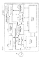
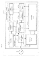
- a wireless power supply system 100 according to one or more embodiments of a first example of the present invention will be described with reference to FIG. 1 to FIG. 5 .
- the wireless power supply system 100 may comprise a power supply device 101.
- the power supply device 101 is disposed, for example, on the ground or the like.
- the power supply device 101 includes a power supply coil 111a, and the power supply coil 111a is disposed on a power receiving device 2 side (upper side) that will be described below of the power supply device 101.
- the power supply device 101 is an example of a "wireless power supply device" of embodiments of the present invention.
- the wireless power supply device may be also called a non-touch power supply device.
- the wireless power supply system may be also called a non-touch power supply system.
- the wireless power supply system 100 may comprise a power receiving device 2.
- the power receiving device 2 is disposed, for example, inside an electric automobile 2a.
- the electric automobile 2a is parked near (above) where the power supply device 101 is disposed.
- a power receiving coil 21a is provided on a power supply device 101 side (ground side) of the power receiving device 2.
- the power supply coil 111a and the power receiving coil 21 a are provided so as to oppose each other.
- the power supply device 101 may comprise a resonant circuit 111.
- the resonant circuit 111 includes the power supply coil 111a and a resonant capacitor 111b.
- the power supply coil 111a supplies power to the power receiving coil 21a by generating a powered magnetic field by power supplied from an AC/DC power source unit 114 that will be described below.
- the resonant capacitor 111b is connected to the power supply coil 111a in series, and in a situation where a voltage of an alternating current having a resonance frequency is applied, resonates in series (impedance is minimized).
- the power supply device 101 may comprise a controller 112.
- the controller 112 includes a CPU (Central Processing Unit) and controls an entirety of the power supply device 101, such as an oscillation circuit 113 that will be described below.
- CPU Central Processing Unit
- the power supply device 101 may comprise the oscillation circuit 113.
- the oscillation circuit 113 outputs a drive signal S1 having a high-frequency drive frequency f1 based on a command of the controller 112.
- the high-frequency drive frequency f1 is set to a frequency (6.78 MHz) established by a standard or the like (A4WP or the like).
- the oscillation circuit 113 outputs a comparison signal S2 whose phase is delayed (or sped up) 90 degrees from the drive signal S1 with a phase of the drive signal S1 as reference (phase 0 degrees).
- a resonant frequency f2 of the resonant circuit 111 is greater than the drive frequency f1 of the drive signal. That is, a size of an inductance of the power supply coil 111a and a capacitance value of the resonant capacitor 111b are set to values such that the resonant frequency f2 of the resonant circuit 111 becomes greater than the drive frequency f1 (6.78 MHz) of the drive signal.
- the power supply device 101 includes the AC/DC power source unit 114.
- the AC/DC power source unit 114 acquires power of an alternating current from a commercial power source 3 provided on the outside and rectifies the acquired power into a direct current to output the power. Moreover, the AC/DC power source unit 114 can change an output voltage value based on a command from the controller 112.
- the power supply device 101 may comprise a gate drive circuit 115. Moreover, the power supply device 101 may comprise an FET (Field Effect Transistor) 116a and an FET 116b.
- the gate drive circuit 115 is connected to the FET 116a and the FET 116b.
- the FET 116a and the FET 116b can turn on and off a direct current voltage applied to the resonant circuit 111 from the AC/DC power source unit 114.
- the gate drive circuit 115 acquires the drive signal S1 from the oscillation unit 113 and, according to the acquired drive signal S1, turns the FET 116a and the FET 116b on and off so one from among the FET 116a and the FET 116b enters a state of being turned on and the other enters a state of being turned off.
- the gate drive circuit 115 is configured as a so-called half bridge circuit; it converts the voltage of a direct current from the AC/DC power source unit 114 into a voltage of an alternating current and outputs this to the resonant capacitor 111b and the power supply coil 111a.
- the power supply device 101 may comprise a switch 117.
- the switch 117 includes an FET or the like and is provided between the FET 116a and FET 116b and the power supply coil 111a.
- the switch 117 switches between a state where the resonant circuit 111 is cut off (off) and a state where the resonant circuit 111 is conducted (on) based on a command from a switch controller 118 that will be described below.
- the power supply device 101 includes the switch controller 118.
- the switch controller 118 includes a phase comparator 118a, a capacitor voltage detector 118b, and a switch drive unit 118c.
- the phase comparator 118a and the capacitor voltage detector 118b are examples of the "voltage phase detector" one or more embodiments of the present invention.
- the capacitor voltage detector 118b is configured to be able to detect a voltage value of a capacitor voltage V C and a phase of the capacitor voltage V C of the resonant capacitor 111b. That is, the capacitor voltage detector 118b can acquire a waveform of the capacitor voltage V C . Moreover, the capacitor voltage detector 118b transmits the acquired waveform of the capacitor voltage V C to the phase comparator 118a.
- the switch controller 118 controls a time T1 of turning off the switch 117 so a phase difference ⁇ 1 between a phase of the drive signal S1 that drives the resonant circuit 111 and a phase of a coil current I L that flows through the power supply coil 111a becomes substantially 0.
- the phase comparator 118a of the switch controller 118 includes a phase difference detector 1181a, an integration unit 1181b, and a coefficient multiplication unit 1181c.
- the phase difference detector 1181 a acquires a comparison signal S2 from the oscillation circuit 113. Moreover, the phase difference detector 1181a acquires the waveform of the capacitor voltage V C . Moreover, the phase difference detector 1181 a detects the phase difference ⁇ 1 by comparing the acquired comparison signal S2 and the acquired capacitor voltage V C .
- phase difference between the phase of the coil current I L that flows through the power supply coil 111a and the phase of the capacitor voltage V C becomes 90 degrees. That is, the phase difference ⁇ 1 between the phase of the capacitor voltage V C and a phase of the comparison signal S2 (90 degree phase difference from the drive signal S1) and the phase difference ⁇ 1 between the phase of the drive signal S1 and the phase of the coil current I L that flow through the power supply coil 111a have the same value.
- the integration unit 1181b acquires the phase difference ⁇ 1 from the phase difference detector 1181a and performs integration. Moreover, the coefficient multiplication unit 1181c calculates the time T1 of turning off the switch 117 by multiplying a predetermined coefficient to a value of the phase difference ⁇ 1 integrated by the integration unit 1181b. That is, the phase comparator 118a is configured to perform a so-called PI (Proportional Integral) control.
- PI Proportional Integral
- the phase difference ⁇ 1 in a situation where the phase difference ⁇ 1 does not become substantially 0 after the switch drive unit 118c turns off the switch 118 for the time T1, with the phase comparator 118a, a value based on the phase difference ⁇ 1 that is not substantially 0 is added to (subtracted from) the time T1. Moreover, by repeating this addition (subtraction), the time T1 converges into a time T2, and the phase difference ⁇ 1 becomes substantially 0.
- the time T2 is an example of the "predetermined time" of embodiments of the present invention.
- the switch drive unit 118c acquires the capacitor voltage V C from the capacitor voltage detector 118b and acquires information of the time T1 from the phase comparator 118a. Moreover, the switch drive unit 118c turns the switch 117 on and off based on the acquired capacitor voltage V C and information of the time T1.
- the power receiving device 2 may comprise a resonant circuit 21.
- the resonant circuit 21 includes the power receiving coil 21a and resonant capacitors 21b and 21c. Moreover, the power receiving coil 21 a receives power by the powered magnetic field generated by the power supply coil 111a.
- the resonant capacitor 21b is connected in series to the power receiving coil 21a. Moreover, the resonant capacitor 21c is connected in parallel to the power receiving coil 21a. Moreover, a capacity of the resonant capacitor 21b and 21c is established according to a load resistance value of a DC/DC converter 23 and a secondary battery 24, which will be described below. Moreover, a resonant frequency f3 of the resonant circuit 21, similarly to the drive frequency f1 of the drive signal S1 of the power supply device 101, is set to a frequency (6.78 MHz) established by a standard or the like (A4WP or the like).
- the resonant frequency f3 of the resonant circuit 21 and the drive frequency f1 of the drive signal S1 are set to be substantially equal.
- the power supply device 101 and the power receiving device 2 can perform power supply by a so-called magnetic resonance method.
- the power receiving device 2 may comprise a rectification circuit 22.
- the rectification circuit 22 includes a plurality of diodes and the like and rectifies an alternating current of the power received by the power receiving coil 21a into a direct current.
- the power receiving unit 2 may comprise the DC/DC converter 23.
- the DC/DC converter 23 converts a voltage value of the rectified direct current into a constant voltage value of a direct current suited for charging the secondary battery 24 that will be described below.
- the power receiving device 2 may comprise the secondary battery 24.
- the secondary battery 24 charges the power supplied from the DC/DC converter 23.
- the capacitor voltage V C gradually increases. Moreover, the comparison signal S2 is turned on. Then, at point t2, the capacitor voltage V C becomes a maximum value.
- the capacitor voltage V C gradually decreases. Then, at point t4, the capacitor voltage V C becomes substantially 0. Moreover, because the resonant frequency f2 of the resonant circuit 111 is greater than the drive frequency f1 of the drive signal S1 (comparison signal S2), the comparison signal S2 is turned off at point t5 (after point t4). In this situation, the phase difference between the phase of the capacitor voltage V C and the phase of the comparison signal S2 becomes the phase difference ⁇ 1.
- the capacitor voltage V C of the wireless power supply system 100 before the switch 117 is driven includes an amplitude A1.
- the capacitor voltage V C gradually increases. Moreover, the comparison signal S2 is turned on. Then, at point t2, the capacitor voltage V C becomes a maximum value.
- the phase difference ⁇ 1 between the phase of the drive signal S1 (comparison signal S2) and the phase of the coil current I L (capacitor voltage V C ) that flows through the power supply coil 111a becomes substantially 0.
- on and off of the switch 117 is switched at a point (point t2 and point t6) when an energy E1 stored in the resonant circuit 111 enters a state of not being stored in the power supply coil 111a but being stored in the resonant capacitor 111b.
- the energy E1 can be expressed by the following formula (1).
- E1 1/2 ⁇ C ⁇ V C 2 + 1/2 ⁇ L ⁇ I L 2 ...(1)
- the capacitor voltage V C gradually decreases. Then, at point t5, the capacitor voltage V C becomes substantially 0. Moreover, the comparison signal S2 is also turned off at point t5. In this situation, the phase difference ⁇ 1 between the phase of the capacitor voltage V C and the phase of the comparison signal S2 becomes substantially 0.
- the capacitor voltage V C becomes equal to the value at point t1. Therefore, a period of the waveform of the capacitor voltage V C becomes a period from point t1 to point t9 and becomes equal to a period of the comparison signal S2 (drive signal S1). That is, the frequency of the capacitor voltage V C (resonant frequency f2 of the resonant circuit 111) is artificially changed to a value equal to the drive frequency f1 of the drive signal S1.
- the capacitor voltage V C includes an amplitude A2. Moreover, the amplitude A2 becomes greater than the amplitude A1 before driving of the switch 117. That is, the drive frequency f1 and the resonant frequency f2 of the resonant circuit 111 becoming equal values signifies that the impedance of the resonant circuit 111 is become smaller compared to before the switch 117 is driven.
- the power supply device 101 may comprise the resonant circuit 111 that includes the power supply coil 111a and the resonant capacitor 111b, changes the waveform of the power (capacitor voltage V C ) in the resonant circuit, and controls the phase difference between the phase of the drive signal S1 that drives the resonant circuit 111 and the phase of the waveform of the current I L that flows through the power supply coil 111a to be substantially 0.
- the switch 117 is connected to the resonant circuit 111.
- the switch controller 118 controls the time T1 of turning off the switch 117 so the phase difference ⁇ 1 between the phase of the drive signal S1 that drives the resonant circuit 111 and the phase of the coil current I L that flows through the power supply coil 111a becomes substantially 0.
- the switch controller 118 controls the time T1 of turning off the switch 117 so the phase difference ⁇ 1 between the phase of the drive signal S1 that drives the resonant circuit 111 and the phase of the coil current I L that flows through the power supply coil 111a becomes substantially 0.
- the switch 117 connected to the resonant circuit 111 is turned off so as to cut off the resonant circuit 111, and the state where the energy E1 is stored in the resonant capacitor 111b can be maintained.
- the resonant frequency f2 of the resonant circuit 111 can be artificially changed during the time T1 (time T2) when the switch 117 is turned off.
- the resonant frequency f2 of the resonant circuit 111 and the resonant frequency f3 (drive frequency f1) of the power receiving device 2 can be made substantially equal without using a varicap.
- a comparatively large power can be efficiently power supplied even in a situation where the resonant frequency f2 of the resonant circuit 111 is different from the resonant frequency f3 of the power receiving device 2.
- the resonant circuit 111 may be configured so the resonant frequency f2 of the resonant circuit 111 becomes greater than the drive frequency f1 of the drive signal S1.
- the switch controller 118 is configured to turn the switch 117 on and off and, by changing the waveform of the power (capacitor voltage V C ) of the resonant circuit 111 having the resonant frequency f2, perform a control of making the phase difference ⁇ 1 between the phase of the drive signal S1 and the phase of the coil current I L that flows through the power supply coil 111a substantially 0.
- the switch 117 connected to the resonant circuit 111 is turned off so as to cut off the resonant circuit 111, the waveform of the coil current I L that flows through the power supply coil 111a having the resonant frequency f2 (waveform of the capacitor voltage V C applied to the resonant capacitor 111b) can be extended during the time T1 (time T2) of being turned off.
- the resonant frequency f2 of the resonant circuit 111 can easily be artificially made smaller.
- the resonant frequency f2 of the resonant circuit 111 becomes greater than the drive frequency f1 of the drive signal and artificially decreasing the resonant frequency f2 of the resonant circuit 111, the resonant frequency f2 of the resonant circuit 111 and the resonant frequency f3 (drive frequency f1) of the power receiving device 2 can easily be made substantially equal.
- the power supply device 101 includes the capacitor voltage detector 118b and phase comparator 118a that can detect the phase of the capacitor voltage V C of the resonant capacitor 111b.
- the switch controller 118 is configured to control the time T1 of turning off the switch 117 so the phase difference between the phase of the drive signal S1 and the phase of the capacitor voltage V C becomes substantially 90 degrees (so the phase difference between the phase of the comparison signal S2 and the phase of the capacitor voltage V C becomes substantially 0).
- the phase difference between the phase of the capacitor voltage V C and the phase of the coil current I L that flows through the power supply coil 111a is 90 degrees.
- the capacitor voltage detector 118b and the phase comparator 118a that can detect the phase of the capacitor voltage V C , compared to a detector (for example, a current sensor) that can detect the phase of the coil current I L that flows through the power supply coil 111a, can be provided easily. Therefore, by providing a capacitor voltage detector 118b and phase comparator 118a having a configuration such as above, the power supply device 101 can be configured easily, and the phase difference ⁇ 1 between the phase of the drive signal S1 and the phase of the coil current I L that flows through the power supply coil 111a (phase 90 degrees different from the phase of the capacitor voltage V C ) can be detected.
- the switch 117 is connected to the resonant circuit 111 so switching is enabled between the state where the resonant circuit 111 is cut off and the state where the resonant circuit 111 is conducted. Because current can be suppressed from flowing in the resonant circuit 111 thereby when the resonant circuit 111 is cut off, the waveform of the coil current I L that flows through the power supply coil 111a (waveform of the capacitor voltage V C ) can be changed easily. As a result, the phase difference between the phase of the drive signal S1 and the phase of the coil current I L that flows through the power supply coil 111a can be made to be substantially 0.
- the switch controller 118 may be configured so by turning off the switch 117 for the time T2 at point t2 when the capacitor voltage V C is maximized and at point t6 when it is minimized, the phase difference ⁇ 1 between the phase of the drive signal S1 and the phase of the coil current I L that flows through the power supply coil 111a becomes substantially 0.
- the current that flows through the resonant circuit 111 (coil current I L ) becomes substantially 0. Therefore, because the switch 117 can be turned off for the time T2 when the current that flows through the resonant circuit 111 is substantially 0 by being configured as above, loss of the energy E1 generated when the switch 117 is turned off can be reduced.
- the switch controller 118 may perform the control of switching on and off of the switch 117 at the point (point t2 and point t6) when the energy E1 stored in the resonant circuit 111 enters the state of not being stored in the power supply coil 111a but being stored in the resonant capacitor 111b.
- the point (point t2 and point t6) when the state is entered into of not being stored in the power supply coil 111a but being stored in the resonant capacitor 111b, the state is entered into where the current that flows through the resonant circuit 111 (coil current I L ) becomes substantially 0. Therefore, because the switch 117 can be turned on and off when the current that flows through the resonant circuit 111 becomes substantially 0 by being configured as above, loss of the energy E1 generated when the switch 117 is turned on and off can be reduced.
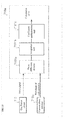
- a wireless power supply system 200 according to embodiments of a second example of the present invention will be described with reference to FIG. 1 and FIG. 7 .
- a switch is connected in parallel to the power supply coil so as to enable shorting the power supply coil.
- the wireless power supply system 200 may comprise a power supply device 201.
- the power supply device 201 may comprise an oscillation circuit 213.
- the power supply device 201 may comprise a resonant circuit 211.
- the resonant circuit 211 includes the power supply coil 111a, the resonant capacitor 111b, and a switch 217.
- the switch 217 is connected in parallel to the power supply coil 111a so as to enable shorting the power supply coil 111a. That is, in a situation where the switch 217 is turned on, both ends of the power supply coil 111a are shorted, and a potential difference between both ends of the power supply coil 111a becomes 0.
- the power supply device 201 may comprise a switch controller 218.
- the switch controller 218 includes a phase comparator 218a, a coil current detector 218b, and a switch drive unit 218c.
- the coil current detector 218b includes a current sensor and the like and acquires the waveform (current value and phase) of the coil current I L of the power supply coil 111a.
- the phase comparator 218a acquires the waveform of the coil current I L from the coil current detector 218b and acquires the comparison signal S3 from the oscillation circuit 213.
- the phase comparator 218a based on the acquired waveform of the coil current I L and comparison signal S3, calculates a phase difference ⁇ 2 and a time T3 of turning on the switch 217.
- the phase comparator 218a transmits information of the time T3 to the switch drive unit 218c.
- the switch drive unit 218c acquires the information of the time T3 from the phase comparator 218a and the coil current I L from the coil current detector 218b and, based on the acquired time T3 from the phase comparator 218a and the coil current I L from the coil current detector 218b, turns the switch 217 on and off.
- Other configurations of the wireless power supply system 200 according to embodiments of the second example of the present invention are similar to those of the wireless power supply system 100 according to embodiments of the first example of the present invention.
- the coil current I L gradually increases. Moreover, the comparison signal S3 is turned on. Then, at point t12, the coil current I L becomes a maximum value.
- the phase difference ⁇ 2 between the phase of the drive signal S1 (comparison signal S3) and the phase of the coil current I L that flows through the power supply coil 111a is made to be substantially 0.
- on and off of the switch 217 is switched at a point (point t12 and point t16) when a state is entered into where an energy E2 stored in the resonant circuit 211 is not stored in the resonant capacitor 111b but stored in the power supply coil 111a.
- the switch 217 is turned on.
- the power supply coil 111a and resonant capacitor 111b voltage values are substantially 0, loss of the energy E2 by the power supply coil 111a being shorted is substantially 0.
- the power supply coil 111a is shorted, the coil current I L does not change in the period from point t12 to point t13.
- the coil current I L gradually decreases. Then, at point t15, the coil current I L becomes substantially 0. Moreover, the comparison signal S3 is also turned off at point t15. In this situation, the phase difference ⁇ 2 between the phase of the coil current I L and the phase of the comparison signal S3 becomes substantially 0.
- the phase difference ⁇ 2 before the switch 217 is driven is a phase that corresponds to point t14 to point t15.
- the coil current I L becomes equal to a value at point t11. Therefore, a period of the waveform of the coil current I L becomes a period from point t11 to point t17 and becomes equal to a period of the comparison signal S3 (drive signal S1). That is, the resonant frequency f2 of the resonant circuit 211 is changed artificially to a value equal to the drive frequency f1 of the drive signal S 1.
- the switch 217 is connected in parallel to the power supply coil 111a so as to enable shorting the power supply coil 111a. Because a size of the coil current I L that flows through the power supply coil 111a can thereby be maintained while the power supply coil 111a is shorted, the waveform of the coil current I L that flows through the power supply coil 111a can be changed easily. As a result, the phase difference ⁇ 2 between the phase of the drive signal S1 and the phase of the coil current I L that flows through the power supply coil 111a can easily be made to be substantially 0.
- the switch controller 218 is configured so by turning on the switch 217 for the time T3 at point t12 when the current value of the coil current I L is maximized and at point t16 when it is minimized, the phase difference ⁇ 2 between the phase of the drive signal S1 and the phase of the coil current I L that flows through the power supply coil 111a becomes substantially 0.
- the voltage value of the power supply coil 111a and the voltage value of the resonant capacitor 111b become substantially 0.
- the switch 217 can be turned on for the time T3 when the voltage value of the power supply coil 111a and the voltage value of the resonant capacitor 111b become substantially 0 by being configured as above, loss of energy generated when the switch 217 is turned on can be reduced.
- other effects of the wireless power supply system 200 according to embodiments of the second example of the present invention are similar to those of the wireless power supply system 100 according to embodiments of the first example of the present invention.
- a wireless power supply system 300 according to one or more embodiments of a third example of the present invention will be described with reference to FIG. 1 and FIG. 9 .
- a gate drive circuit and FET unlike the wireless power supply system 100 according to embodiments of the first example of the present invention where the gate drive circuit and FET that switch the power supplied form the AC/DC power source unit and the switch are configured separately, a gate drive circuit and FET are configured to also function as a switch.
- the wireless power supply system 300 may comprise a power supply device 301.
- the power supply device 301 includes a gate drive circuit 315, FETs 316a and 316b, and a switch controller 318.
- the gate drive circuit 315 and the FETs 316a and 316b are examples of the "power converter" of embodiments of the present invention.
- the gate drive circuit 315 and the FETs 316a and 316b that convert the power supplied from the AC/DC power source unit 114 into power of an alternating current based on the drive signal S1 by switching the power supplied from the AC/DC power source unit 114 and supply this to the resonant circuit 111 as the power for generating the powered magnetic field are configured to also function as a switch.
- the gate drive circuit 315 acquires a signal for driving the switch (switch drive signal) from the switch controller 318 and turns off both FETs 316a and 316b for the time T2. Moreover, the gate drive circuit 315 turns off both FETs 316a and 316b for the time T2 at a point similar to the point when the switch drive unit 118c according to embodiments of the first example of the present invention turns off the switch 117.
- the gate drive circuit 315 and the FETs 316a and 316b similarly to the switch 117 according to embodiments of the first example of the present invention, can switch between the state where the resonant circuit 111 is cut off and the state where the resonant circuit 111 is conducted.
- other configurations of the wireless power supply system 300 according to embodiments of the third example of the present invention are similar to those of the wireless power supply system 100 according to embodiments of the first example of the present invention.
- the gate drive circuit 315 and the FETs 316a and 316b that convert the power supplied from the AC/DC power source unit 114 into the power of an alternating current based on the drive signal S1 by switching the power supplied from the AC/DC power source unit 114 and supply this to the resonant circuit 111 as the power for generating the powered magnetic field are configured to also function as the switch.
- the gate drive circuit 315 and FETs 316a and 316b and the switch do not need to be provided separately, a component count of the power supply device 301 can be suppressed from increasing.
- other effects of the wireless power supply system 300 according to emobodiments of the third example of the present invention are similar to those of the wireless power supply system 100 according to embodiments of the first example of the present invention.
- a wireless power supply system 400 according to a fourth example will be described with reference to FIG. 1 and FIG. 2 .
- the switch is turned off at every point when the capacitor voltage is maximized and minimized, the switch is not turned off at a point when the capacitor voltage is minimized, and the switch is turned on every two periods at a point when the capacitor voltage is maximized.
- the wireless power supply system 400 may comprise a power supply device 401.
- the power supply device 401 includes a switch controller 418.
- the switch controller 418 includes the capacitor voltage detector 118b, a phase comparator 418a, and a switch drive unit 418c.
- the capacitor voltage detector 118b similarly to the capacitor voltage detector 118b of the first example of the present invention, can acquire the waveform (voltage value and phase) of the capacitor voltage V C of the resonant capacitor 111b.
- the phase comparator 418a based on the waveform of the capacitor voltage V C and the comparison signal S2, calculates a time T4 of turning off the switch 117.
- the switch drive unit 418c based on the time T4 and the capacitor voltage V C , turns the switch 117 on and off.
- other configurations of the wireless power supply system 400 according to embodiments of the fourth example of the present invention are similar to those of the wireless power supply system 100 according to embodiments of the first example of the present invention.
- the phase difference ⁇ 3 between the phase of the drive signal S1 and the phase of the coil current I L that flows through the power supply coil 111a (phase difference ⁇ 3 between the phase of the comparison signal S2 and the capacitor voltage V C ) is made to be substantially 0. This will be described in detail below.
- the capacitor voltage V C gradually increases. Moreover, the comparison signal S2 is turned on. Then, at point t22, the capacitor voltage V C becomes a maximum value.
- the switch 117 is turned off for the time T4. That is, at point t26, which is one period after point t23, the switch 117 is not turned off, and the switch 117 is turned on at point t27, which is two periods after point t23.
- the phase difference ⁇ 3 between the phase of the comparison signal S2 and the capacitor voltage V C is made to be substantially 0.
- the frequency of the capacitor voltage V C (resonant frequency f2 of the resonant circuit 111) is artificially changed to a value equal to the drive frequency f1 of the drive signal S1.
- the switch controller 418 by turning the switch 117 off for the time T4 not at every point when the capacitor voltage V C is at least maximized or minimized but at a portion of these points (points t22 and t27), the phase difference ⁇ 3 between the phase of the drive signal S1 and the phase of the coil current I L that flows through the power supply coil 111a (phase difference ⁇ 3 between the phase of the comparison signal S2 and the capacitor voltage V C ) is made to be substantially 0.
- a configuration of a wireless power supply system 500 according to a fifth example will be described with reference to FIG. 1 and FIG. 11 .
- a switching circuit of a so-called H bridge type configured by a gate drive circuit and four FETs is provided.
- the wireless power supply system 500 may comprise a power supply device 501.
- the power supply device 501 includes a gate drive circuit 515 and FETs 516a to 516d.
- a drain of the FET 516a is connected to an output side of the AC/DC power source unit 114. Moreover, a source of the FET 516a and a drain of the FET 516b are connected to the switch 117. Moreover, a source of the FET 516b is grounded.
- a drain of the FET 516c is connected to the output side of the AC/DC power source unit 114. Moreover, a source of the FET 516c and a drain of the FET 516d are connected to the power supply coil 111a. Moreover, a source of the FET 516d is grounded.
- the gate drive circuit 515 and the FETs 516a to 516d are configured as the so-called H bridge circuit; it converts a voltage of a direct current from the AC/DC power source unit 114 (for example, a voltage value Vt) into a voltage of an alternating current having the drive frequency f1 (rectangular wave having a voltage value +Vt and a voltage value -Vt) and outputs this to the resonant capacitor 111b and the power supply coil 111a.
- the power supply device 501 may comprise the gate drive circuit 515 and the FETs 516a to 516d.
- the gate drive circuit 515 and the FETs 516a to 516d can be driven as the switching circuit of the so-called H bridge type.
- a size of a voltage value supplied to the power supply coil 111a can be doubled (-Vt to +Vt).
- a configuration of a wireless power supply system 600 according to a sixth example will be described with reference to FIG. 1 and FIG. 12 .
- a variable amplifier configured to be able to amplify an alternating current of a sine wave is provided.
- the wireless power supply system 600 may comprise a power supply device 601.
- the power supply device 601 may comprise a controller 612, an AC/DC power source unit 614, a sine wave generator 615a, and a variable amplifier 615b.
- the AC/DC power source unit 614 unlike the AC/DC power source unit 114 according to embodiments of the first example of the present invention, outputs a constant voltage value. Moreover, the AC/DC power source unit 614 is connected to the variable amplifier 615b and supplies power to the variable amplifier 615b.
- the sine wave generator 615a acquires the drive signal S1 from the oscillation circuit 113 and outputs a sine wave having the drive frequency f1 of the acquired drive signal S1. Moreover, an output side of the sine wave generator 615a is connected to an input side of the variable amplifier 615b.
- variable amplifier 615b acquires the sine wave having the drive frequency f1 from the sine wave generator 615a. Moreover, the variable amplifier 615b amplifies the acquired sine wave into power having a voltage value in accordance with a command from the controller 612 using the power supplied from the AC/DC power source unit 614. Moreover, the output side of the variable amplifier 615b is connected to the switch 117 and outputs power to the resonant capacitor 111b and the power supply coil 111a.
- the power supply device 601 may comprise the AC/DC power source unit 614, the sine wave generator 615a, and the variable amplifier 615b.
- the alternating voltage of the sine wave can be imparted to the power supply coil 111a.
- high-frequency noise becomes less likely to be generated, and therefore, electromagnetic interference to surrounding equipment by the high-frequency noise can be reduced form increasing.
- other effects of the wireless power supply system 600 according to embodiments of the sixth example of the present invention are similar to those of the wireless power supply system 100 according to embodiments of the first example of the invention.
- the power receiving device of embodiments of the present invention is applied in an electric automobile, but the present invention is not limited thereto.
- the power receiving device may be applied to equipment other than an electric automobile.
- it may be applied in a mobile phone device such as a smart phone such as that illustrated in FIG. 15 that will be described below.
- the capacitor voltage detector is provided and the phase difference between the phase of the capacitor voltage and the comparison signal is made to be acquired, but the present invention is not limited thereto.
- a coil voltage detector may be provided to acquire a phase difference between a phase of a coil voltage and the comparison signal.
- a coil voltage detector 118b-1 is provided in a power supply device 101-1 according to embodiments of a modified example of the first example of the present invention illustrated in FIG. 13 .
- the power supply device 101-1 may comprise a resonant circuit 111-1 and a coil voltage detector 118b-1.
- the resonant circuit 111-1 includes a power coil 111a-1 and a resonant capacitor 111b-1.
- the coil voltage detector 118b-1 acquires a waveform of a coil voltage V L .
- a phase difference between a phase of the coil voltage V L and the phase of the coil current I L that flows through the power supply coil 111a-1 is 90 degrees.
- the power supply device 101-1 artificially changes the resonant frequency f2 of the resonant circuit 111 to a value equal to the drive frequency f1 of the drive signal S1 by making the phase difference between a phase of a comparison signal S4 having a phase difference of 90 degrees with the drive signal S1 and the phase of the coil voltage V L .
- the switch is turned off the predetermined time at every point when the voltage value of the resonant capacitor is maximized and minimized or at one point every two periods when the voltage value of the resonant capacitor is maximized, but the present invention is not limited thereto.
- the switch may be configured to be turned off a predetermined time at every point when the voltage value of the resonant capacitor is maximized and minimized or at a point other than the one point every two periods when the voltage value of the resonant capacitor is maximized.
- the switch 117 is turned off a time T5 at one point every one period when the coil voltage value V L of the power supply coil 111a-1 is maximized.
- the power supply device 101-1 may comprise a switch controller 118-1.
- the switch controller 118-1 includes a phase comparator 718a, a coil voltage detector 118b-1, and a switch drive unit 718c.
- the switch controller 118-1 turns off the switch 117 for the time T5 at every point when the coil voltage value V L of the power supply coil 111a-1 is maximized (one point every one period, such as points t31 to t32 and points t33 to t34).
- embodiments of the first to sixth examples of the present invention describe configurations separately, but a form of the present invention is not limited to the above embodiments.
- the present invention may be configured by combining embodiments of the first to sixth examples of the present invention with each other.
- an example is illustrated of providing the switch to enable switching between the state of cutting off and the state of conducting the resonant circuit, but the present invention is not limited thereto.
- the configuration of one or more embodiments of the fourth to sixth examples of the present invention and the configuration of one or more embodiments of the second example of the present invention of providing the switch in parallel to the power supply coil and shorting both ends of the power supply coil may be combined.
- a wireless power supply system 700 according to one or more embodiments of a seventh example of the present invention will be described with reference to FIG. 5 and FIG. 15 to FIG. 18 .
- the wireless power supply system 700 may comprise a power supply device 701.
- the power supply device 701 is configured so the power receiving device 2 can be disposed on an upper surface of the power supply device 701.
- a power supply coil 711a is disposed inside the power supply device 701.
- the power supply device 701 is an example of the "wireless power supply device" of the present invention.
- the wireless power supply system 700 may comprise the power receiving device 2.
- the power receiving device 2 is disposed on the upper surface of the power supply device 701.
- the power receiving device 2 includes the power receiving coil 21a.
- a power supply coil 711a and the power receiving coil 21a are provided so as to oppose each other.
- the power receiving device 2 illustrated in FIG. 15 is, for example, a mobile telephone device such as a smart phone.
- the power supply device 701 may comprise a resonant circuit 711.
- the resonant circuit 711 includes the power supply coil 711a and a capacitor 711b.
- the power supply coil 711a supplies power to the power receiving coil 21a by generating a powered magnetic field by power supplied from an AC/DC power source unit 714.
- the resonant capacitor 711 b is connected to the power supply coil 711a in series, and in a situation where a voltage of an alternating current having a resonance frequency is applied, resonates in series (an impedance becomes minimized).
- the power supply device 701 may comprise a first sub capacitor 712a connected in parallel to the resonant capacitor 711b. Moreover, the power supply device 701 is connected in series to the first sub capacitor 712a and may comprise a first switch 712b that can switch between connection and disconnection between the resonant capacitor 711b and the first sub capacitor 712a.
- the power supply device 701 may comprise a second sub capacitor 712c connected in parallel to the resonant capacitor 711b. Moreover, the power supply device 701 is connected in series to the second sub capacitor 712c and may comprise a second switch 712d that can switch between connection and disconnection between the resonant capacitor 711b and the second sub capacitor 712c.
- the power supply device 701 includes a controller 712.
- the controller 712 includes a CPU and controls an entirety of the power supply device 701, such as an oscillation circuit 713 that will be described below.
- the power supply device 701 includes the oscillation circuit 713.
- the oscillation circuit 713 outputs a drive signal having the high-frequency drive frequency f1 based on a command of the controller 712.
- the high-frequency drive frequency f1 is set to a frequency established by a standard or the like.
- the drive frequency f1 is set to 100 kHz.
- a capacitance value of the resonant capacitor 711b is a capacitance value such as one where the resonant frequency f2 of the power supply coil 711a and the resonant capacitor 711b (resonant circuit 711) becomes greater than the drive frequency f1 of the drive signal that drives the power supply coil 711a and the resonant capacitor 711b.
- a size of an inductance of the power supply coil 711 a and a capacitance value of the resonant capacitor 711 b are set to values such that the resonant frequency f2 of the resonant circuit 711 becomes greater than the drive frequency f1 (100 kHz) of the drive signal.
- the capacitance of the resonant capacitor 711b is configured to be 0.012 ⁇ F and the resonant frequency f2 of the resonant circuit 711 is set to be 119 kHz.
- the capacitance values of the first sub capacitor 712a and the second sub capacitor 712c are both set to 0.010 ⁇ F.
- the capacitance value becomes 0.022 ⁇ F.
- the resonant frequency f2 of the resonant circuit 711 becomes 88 kHz.
- the resonant frequency f2 of the resonant circuit 711 becomes 88 kHz.
- the power supply device 701 includes the AC/DC power source unit 714.
- the AC/DC power source unit 714 acquires power of an alternating current from the commercial power source 3 provided on the outside and rectifies the acquired power into a direct current to output the power. Moreover, the AC/DC power source unit 714 changes an output voltage value based on a command from the controller 712.
- the power supply device 701 includes a switching circuit 716.
- the switching circuit 716 includes a plurality of FETs and turns on and off a direct current voltage applied to the resonant circuit 711 from the AC/DC power source unit 714.
- the switching circuit 716 is configured as a so-called half bridge circuit, H bridge circuit, or the like.
- the switching circuit 716 acquires the drive signal from the oscillation circuit 713, converts the voltage of a direct current from the AC/DC power source unit 714 into a voltage of an alternating current, and outputs this to the resonant capacitor 711b and the power supply coil 711a.
- the power supply device 701 includes a switch controller 718.
- the switch controller 718 includes the phase comparator 718a that detects the phase difference ⁇ 1 between the phase of the drive signal that drives the power supply coil 711a and the resonant capacitor 711b and the phase of the coil current I L that flows through the power supply coil 711a.
- the phase comparator 718a is an example of the "phase difference detector" of embodiments of the present invention.
- the switch controller 718 includes a capacitor voltage detector 718b, the current phase detector 718c, and a switch drive unit 718d. Moreover, as illustrated in FIG. 17 , the current phase detector 718c detects a waveform (phase and current value) of the coil current I L that flows through the power supply coil 711a. Moreover, the current phase detector 718c transmits the acquired waveform of the coil current I L to the phase comparator 718a.
- the capacitor voltage detector 718b can detect the voltage value of the capacitor voltage V C of the resonant capacitor 711b and the phase of the capacitor voltage V C . Moreover, the capacitor voltage detector 718b transmits the acquired waveform of the capacitor voltage V C to the switch drive unit 718d.
- the switch drive unit 718d acquires the capacitor voltage V C from the capacitor voltage detector 718b and acquires information of the time T1 (time when the first switch 712b and the second switch 712b are turned on) that will be described below from the phase comparator 718a. Moreover, the switch drive unit 718d turns the first switch 712b and the second switch 712b on and off based on the acquired capacitor voltage V C and information of the time T 1.
- the switch controller 718 controls the time T1 when the first switch 712b and the second switch 712d are turned on so the phase difference ⁇ 1 between the phase of the drive signal detected by the phase comparator 718a and the phase of the coil current I L that flows through the power supply coil 711a becomes substantially 0.
- the phase comparator 718a of the switch controller 718 includes a phase difference detector 7181a, an integration unit 7181b, and a coefficient multiplication unit 7181 c.
- the phase difference detector 7181 a acquires the drive signal from the oscillation circuit 713.
- the phase difference detector 7181a acquires the waveform of the coil current I L from the current phase detector 718c.
- the phase difference detector 7181 a detects the phase difference ⁇ 1 by comparing the acquired drive signal and the acquired coil current I L .
- the integration unit 7181b acquires the phase difference ⁇ 1 from the phase difference detector 7181 a and performs integration. Moreover, the coefficient multiplication unit 7181c calculates the time T1 of turning on the first switch 712b and the second switch 712d by multiplying a predetermined coefficient to the value of the phase difference ⁇ 1 integrated by the integration unit 7181b. That is, the phase comparator 718a performs so-called PI control.
- phase difference ⁇ 1 does not become substantially 0 after the switch drive unit 718d turns on the first switch 712b and the second switch 712d for the time T1
- phase comparator 718a a value based on the phase difference ⁇ 1 that is not substantially 0 is added to (subtracted from) the time T1.
- the time T1 converges into a predetermined time, and the phase difference ⁇ 1 becomes substantially 0.
- the power receiving device 2 may comprise the configuration illustrated in FIG. 5 .
- the power receiving coil 21a receives power by the powered magnetic field generated by the power supply coil 711 a.
- the resonant frequency f3 of the resonant circuit 21, similarly to the drive frequency f1 of the drive signal of the power supply device 701, is set to a frequency (for example, 100 kHz) established by a standard (for example, Qi standard) or the like.
- the voltage value of the capacitor voltage V C (voltage value of resonant capacitor 711b) becomes a maximum value (peak).
- the current value of the coil current I L is 0.
- the drive signal is turned off.
- the capacitor voltage V C and the coil current I L gradually decrease.
- the capacitor voltage V C becomes 0, and the current value of the coil current I L becomes a minimum value (peak).
- the capacitor voltage V C becomes a minimum value, and the current value of the coil current I L becomes 0.
- the resonant frequency f2 for example, 119 kHz
- the drive frequency f1 for example, 100 kHz
- the capacitor voltage V C becomes the maximum value.
- the coil current I L becomes 0. That is, a period of the capacitor voltage V C and the coil current I L is from point t1 to point t5.
- the drive signal is turned off. That is, a period of the drive signal is from point t1 to point t6.
- the phase difference ⁇ 1 between the phase of the coil current I L and the phase of the drive signal corresponds to a time difference between point t5 and point t6.
- the capacitor voltage V C of the wireless power supply system 700 before the first switch 712b and the second switch 712d are driven includes the amplitude A1.
- the coil current I L includes the amplitude A2.
- the voltage value of the capacitor voltage V C (resonant capacitor 711b) is 0 and the current value of the coil current I L is the maximum value (peak). Moreover, the voltage value of the first sub capacitor 712a is +V1, and the voltage value of the second sub capacitor 712c is -V1.
- the first switch 712b is turned on when the voltage value of the capacitor voltage V C is become a voltage value (+V1) substantially equal to the voltage value of the first sub capacitor 712a near a maximum.
- the capacitor voltage V C becomes +V1. That is, the voltage value of the resonant capacitor 711b and the voltage value of the first sub capacitor 712a become substantially equal voltage values (+V1). Then, at point t12, by a first switch drive signal being turned on by the switch drive unit 718d (put into a high state), the first switch 712b is turned on, and the resonant capacitor 711b and the first sub capacitor 712a are connected. As a result, the resonant frequency of the resonant circuit 711 decreases (for example, in the above example, it changes from 119 kHz to 88 kHz).
- the voltage values of the capacitor voltage V C and the first sub capacitor 712a gradually increase. Then, at point t13, the voltage values of the capacitor voltage V C and the first sub capacitor 712a become maximum values. Moreover, the coil current I L becomes 0. Moreover, the drive signal is also turned off.
- the time T1 of turning on the first switch 712b is controlled so after turning on the first switch 712b when the voltage value of the resonant capacitor 711b and the voltage value of the first sub capacitor 712a are become substantially equal voltage values (+V1), the first switch 712b is turned off at point t14 when the voltage value (+V1) of when the first switch 712b is turned on is again achieved while remaining when the voltage value of the resonant capacitor 711b and the voltage value of the first sub capacitor 712a are substantially equal voltage values.
- both the voltage value of the resonant capacitor 711b and the voltage value of the first sub capacitor 712a become +V1.
- the first switch 712b is turned off. That is, when the voltage value (+V1) of when the first switch 712b is turned on is again achieved, the resonant capacitor 711b and the first sub capacitor 712a are cut off.
- the resonant frequency of the resonant circuit 711 returns to an original size (for example, in the above example, it changes from 88 kHz to 119 kHz).
- the period from point t12 to point t13 (point when the drive signal is turned off) and the period from point t13 to point t14 become substantially the same period.
- the first switch 712b can be turned on and off when the voltage value of the first sub capacitor 712a is continuously +V1 (zero voltage switching).
- the second switch 712d is turned on when the voltage value of the capacitor voltage V C becomes a voltage value substantially equal to the voltage value of the second sub capacitor 712c near a minimum.
- the voltage value of the capacitor voltage V C gradually decreases. Moreover, the coil current I L gradually increases. Moreover, the voltage value of the second sub capacitor 712c is -V1. Moreover, at point t6, the voltage value of the capacitor voltage V C becomes -VI, which is a voltage value substantially equal to -VI, the voltage value of the second sub capacitor 712c. Moreover, the second switch 712d is turned on. As a result, the resonant frequency f2 of the resonant circuit 711 is changed to increase.
- both the voltage value of the resonant capacitor 711b and the voltage value of the second sub capacitor 712c become -V1.
- the second switch 712d is turned off. That is, when the voltage value (-V1) of when the second switch 712d is turned on is again achieved, the resonant capacitor 711b and the second sub capacitor 712c are cut off. As a result, the resonant frequency of the resonant circuit 711 is returned to the original size.
- the voltage value of the capacitor voltage V C becomes a maximum value. That is, a period of the waveform of the voltage (capacitor voltage V C ) of the resonant capacitor 711b becomes from point t13 to point t19. Moreover, the current value of the coil current I L becomes 0 at point t19. That is, the period of the waveform of the coil current I L also becomes from point t13 to point t19. Moreover, the drive signal is turned off at point t19. Therefore, the period of the drive signal also becomes from point t13 to point t19.
- the periods of the capacitor voltage V C , the coil current I L , and the drive signal become substantially equal sizes, and the phase difference ⁇ 1 between the phase of the drive signal that drives the resonant circuit 711 and the phase of the coil current I L that flows through the power supply coil 711a becomes substantially 0.
- the resonant frequency f2 of the resonant circuit 711 artificially becomes a size substantially equal to the drive frequency f1 of the drive signal (resonant frequency f3 of the power receiving device 2).
- the waveform of the voltage (capacitor voltage V C ) of the resonant capacitor 711b may comprise an amplitude A3.
- the amplitude A3 becomes greater than the amplitude A1 (see FIG. 19 ) before driving of the first switch 712b and the second switch 712d. That is, the drive frequency f1 and the resonant frequency f2 of the resonant circuit 711 becoming equal values signifies that an impedance of the resonant circuit 711 is decreased compared to before the first switch 712b and the second switch 712d are driven.
- the waveform of the coil current I L includes an amplitude A4.
- the amplitude A4 also becomes greater than the amplitude A2 (see FIG. 19 ) before driving of the first switch 712b and the second switch 712d due to a reason similar to the reason why the amplitude A3 is become greater than the amplitude A1.
- the first sub capacitor 712a and the second sub capacitor 712c are connected in parallel to the resonant capacitor 711b.
- the first switch 712b is connected in series to the first sub capacitor 712a and switches between connection and disconnection between the resonant capacitor 711b and the first sub capacitor 712a.
- the second switch 712d is connected in series to the second sub capacitor 712c and switches between connection and disconnection between the resonant capacitor 71 1b and the second sub capacitor 712c.
- the resonant frequency f2 of the power supply device 701 which is proportional to the inverse of the square root of the capacitance value, can be decreased.
- the switch controller 718 is configured to control the time T1 when the first switch 712b and the second switch 712d are turned on.
- the resonant frequency f2 of the power supply device 701 can be changed according to the time T1 of turning on the first switch 712b and the second switch 712d.
- the resonant frequency f2 of the power supply device 701 and the resonant frequency f3 of the power receiving device 2 can artificially be made to substantially match.
- the switch controller 718 is configured to perform the control of turning on the first switch 712b or the second switch 712d when the voltage value of the resonant capacitor 711b (capacitor voltage V C ) and the voltage value of the first sub capacitor 712a (+V1) or voltage value of the second sub capacitor 712c (-V1) are become substantially equal voltage values.
- the first switch 712b or the second switch 712d can be turned on without disrupting the waveform (frequency) of the voltage applied to the resonant capacitor 711b, and energy being lost when the first switch 712b or the second switch 712d is turned on can be reduced. As a result, transmission efficiency of power in power supply to the power receiving device 2 from the power supply device 701 can be better maintained.
- the capacitance value of the resonant capacitor 711b is configured to be a capacitance value such as one where the resonant frequency f2 of the power supply coil 711a and the resonant capacitor 711b becomes greater than the drive frequency f1 of the drive signal that drives the power supply coil 711a and the resonant capacitor 711b.
- the capacitance value of the resonant capacitor 711b is configured to be 0.012 ⁇ F so the resonant frequency f2 becomes 119 kHz relative to the drive frequency of 100 kHz.
- the resonant frequency f2 of the power supply device 701 thereby becomes greater than the drive frequency f1 of the drive signal, by decreasing the resonant frequency f2 of the power supply device 701 during the time T1 of turning on the first switch 712b or the second switch 712d (for example, making it 88 kHz), the resonant frequency f2 of the power supply device 701 and the resonant frequency f3 of the power receiving device 2 (drive frequency f1 of the drive signal) can easily be artificially substantially matched.
- the power supply device 701 may comprise the first sub capacitor 712a and the second sub capacitor 712c, which are respectively connected in parallel to the resonant capacitor 711b. Moreover, the power supply device 701 may comprise the first switch 712b connected to the first sub capacitor 712a and the second switch 712d connected to the second sub capacitor 712c.
- the switch controller 718 performs the control of turning on the first switch 712b when the voltage value of the resonant capacitor 711b (capacitor voltage V C ) is become the voltage value (+V1) that is near the maximum and substantially equal to the voltage value of the first sub capacitor 712a and turning on the second switch 712d when the voltage value of the resonant capacitor 711b (capacitor voltage V C ) is become the voltage value (-V1) that is near the minimum and substantially equal to the voltage value of the second sub capacitor 712c.
- the first switch 712b is thereby turned on and off when the voltage value of the resonant capacitor 711b is become near the maximum, with the first sub capacitor 712a, the voltage value (+V1) near the maximum of the voltage value of the resonant capacitor 711b is maintained.
- the second switch 712d is turned on and off when the voltage value of the resonant capacitor 711b is become near the minimum, with the second sub capacitor 712c, the voltage value (-V1) near the minimum of the voltage value of the resonant capacitor 711b is maintained.
- the resonant frequency f2 can be changed twice total from among the waveform of the voltage (capacitor voltage V C ) applied to the resonant capacitor 711b: point t12, when the voltage value of the resonant capacitor 711b and the voltage value of the first sub capacitor 712a become substantially equal voltage values; point t16, when the voltage value of the resonant capacitor 711b and the voltage value of the second sub capacitor 712c become substantially equal voltage values.
- the resonant frequency f2 of the power supply device 701 and the resonant frequency f3 (drive frequency f1) of the power receiving device 2 can be substantially matched more reliably.
- the switch controller 718 is configured to control the time T1 of turning on the first switch 712b so after turning on the first switch 712b when the voltage value of the resonant capacitor 711 b (capacitor voltage V C ) and the voltage value of the first sub capacitor 712a are become substantially equal voltage values (from point t12 to point t14), the first switch 712b is turned off at point t14 when the voltage value of when the switch is turned on is again achieved while remaining when the voltage value of the resonant capacitor 711b and the voltage value of the first sub capacitor 712a are substantially equal voltage values.
- the voltage value (+V1) of the resonant capacitor 711b and the first sub capacitor 712a at point t12 when the first switch 712b is turned on and the voltage value (+V1) of the resonant capacitor 711b and the first sub capacitor 712a at point t14 when the first switch 712b is turned off can be matched.
- the voltage value (+V1) of the first sub capacitor 712a before the first switch 712b is turned on (before point t12) and the voltage value (+V1) of the first sub capacitor 712a after the first switch 712b is turned on and off can be substantially matched. Because the first switch 712b can thereby perform zero voltage switching, loss of energy generated when the first switch 712b is turned on and off can be reduced.
- the power supply device 701 includes the phase comparator 718a that detects the phase difference ⁇ 1 between the phase of the drive signal that drives the power supply coil 711a and the resonant capacitor 711b and the phase of the coil current I L that flows through the power supply coil 711a.
- the switch controller 718 is configured to control the time T1 of turning on the first switch 712b and the second switch 712d so the first switch 712b (second switch 712d) is turned on when the voltage value of the resonant capacitor 711b and the voltage value of the first sub capacitor 712a (second sub capacitor 712c) are become substantially equal voltage values and the phase difference ⁇ 1 between the phase of the drive signal detected by the phase comparator 718a and the phase of the coil current I L becomes substantially 0.
- the drive frequency f1 of the drive signal and the resonant frequency f3 of the power receiving device 2 are set to substantially equal values.
- the state where the phase difference ⁇ 1 between the phase of the drive signal and the phase of the coil current I L becomes the state where the resonant frequency f2 of the power supply device 701 and the drive frequency f1 of the drive signal become substantially equal, the resonant frequency f1 of the power supply device 701 and the resonant frequency f3 of the power receiving device 2 can easily be substantially matched.
- a wireless power supply system 800 according to one or more embodiments of an eighth example of the present invention will be described with reference to FIG. 15 , FIG. 16 , and FIG. 21 .
- a first diode unit and a second diode unit connected in parallel to a first switch and a second switch are further provided.
- the wireless power supply system 800 may comprise a power supply device 801.
- the power supply device 801 may comprise a resonant circuit 811.
- the resonant circuit 811 includes a first diode unit 812e connected in parallel to a first switch 812b and a second diode unit 812f connected in parallel to a second switch 812d.
- the anode of the first diode unit 812e is disposed so as to be connected to the resonant capacitor 711b.
- the cathode of the first diode unit 812e is disposed so as to be connected to a first sub capacitor 812a.
- the cathode of the second diode unit 812f is disposed so as to be connected to the resonant capacitor 711b.
- the anode of the second diode unit 812f is disposed so as to be connected to a second sub capacitor 812c.
- the power supply device 801 may comprise a switch controller 818.
- the switch controller 818 includes the capacitor voltage detector 718b, the current phase detector 718c, a phase comparator 818a, and a switch drive unit 818d.
- the phase comparator 818a based on detection results by the capacitor voltage detector 718b and the current phase detector 718c, calculates the time T2 for making the phase difference ⁇ 2 between the phase of the drive signal and the phase of the coil current I L become substantially 0.
- the switch drive unit 818d turns on the first switch 812b and the second switch 812d for the time T3, which is a time shorter than the time T2 by a predetermined amount.
- other configurations of the wireless power supply system 800 according to embodiments of the eighth example of the present invention are similar to those of the wireless power supply system 700 according to embodiments of the seventh example of the present invention.
- the voltage value of the capacitor voltage V C is 0 and the current value of the coil current I L is a maximum value (peak). Moreover, the voltage value of the first sub capacitor 812a is +V2, and the voltage value of the second sub capacitor 812c is -V2.
- the capacitor voltage V C gradually increases. Moreover, the coil current I L gradually decreases. Moreover, the drive signal is turned on. Moreover, at point t32, the capacitor voltage V C becomes +V2. That is, the voltage value of the resonant capacitor 711b (capacitor voltage V C ) and the voltage value of the first sub capacitor 812a become substantially equal voltage values (+V2).
- the first switch 812b is turned on at point t33 between point t32 and point t34.
- the voltage value of the resonant capacitor 711b and the voltage value of the first sub capacitor 812a become a maximum value (peak). Moreover, the coil current I L becomes 0. Moreover, the drive signal is also turned off.
- both the voltage value of the resonant capacitor 711b and the voltage value of the first sub capacitor 812a become +V2. While the voltage value of the resonant capacitor 711b and the voltage value of the first sub capacitor 812a are substantially equal voltage values, a resonant frequency f4 of the resonant circuit 811 decreases (for example, in the above example, it is changed from 119 kHz to 88 kHz). Moreover, the time interval between point t32 and point t35 is the time T2. Moreover, the time interval between point t33 and point t35 is the time T3.
- the first switch 812b is turned off, and the resonant capacitor 711b and the first sub capacitor 812a are cut off. Moreover, no current flows from the first sub capacitor 812a to the resonant capacitor 711b via the first diode unit 812e. As a result, the resonant frequency f4 of the resonant circuit 811 returns to an original size (for example, in the above example, it changes from 88 kHz to 119 kHz).
- the second switch 812d similarly to the first switch 812b, is turned on at point t36 and turned off at point t37.
- the resonant frequency f4 of the resonant circuit 811 artificially becomes a size substantially equal to the drive frequency f1 of the drive signal (resonant frequency f3 of the power receiving device 2).
- the resonant circuit 811 includes the first diode unit 812e connected in parallel to the first switch 812b and the second diode unit 812f connected in parallel to the second switch 812d.
- current can flow unidirectionally (from the resonant capacitor 711 b to the first sub capacitor 812a) via the first diode unit 812e even when the first switch 812b is turned off.
- current can flow unidirectionally (from the second sub capacitor 812c to the resonant capacitor 711b) via the second diode unit 812f even when the second switch 812d is turned off.
- the resonant capacitor 711b and the first sub capacitor 812a or second sub capacitor 812c can be connected when the voltage value of the resonant capacitor 711b and the resonant value of the first sub capacitor 812a or the voltage value of the second sub capacitor 812c are become substantially equal voltage values.
- a wireless power supply system 900 according to one or more embodiments of a ninth example of the present invention will be described with reference to FIG. 15 and FIG. 23 .
- the duration of the first switch and the second switch being on are controlled so the phase difference between the phase of the drive signal and the phase of the coil current becomes substantially 0, the duration of the first switch and the second switch being on is controlled based on a value of the voltage value of the capacitor voltage before and after the duration of the first switch and the second switch being on is changed.
- the wireless power supply system may comprise a power supply device 901.
- the power supply device 901 includes a controller 912.
- the controller 912 controls an entirety of the power supply device 901 and controls the time T4 when the first switch 712b and the second switch 712d are turned on.
- the controller 912 is an example of the "switch controller" of embodiments of the present invention.
- the power supply device 901 includes a capacitor voltage detector 918b.
- the capacitor voltage detector 918b acquires the waveform of the voltage (capacitor voltage V C ) of the resonant capacitor 711b of the resonant circuit 711. Moreover, the capacitor voltage detector 918b transmits the acquired waveform of the capacitor voltage V C to the controller 912.
- the power supply device 901 includes a switch drive unit 917d.
- the switch drive unit 917d turns the first switch 712b and the second switch 712d on and off based on a command from the controller 912.
- other configurations of the wireless power supply system 900 according to embodiments of the ninth example of the present invention are similar to those of the wireless power supply system 700 according to embodiments of the seventh example of the present invention.
- the time T4 of turning on the first switch 712b and the second switch 712d is changed, values of the voltage value of the resonant capacitor 711 b (capacitor voltage V C ) detected by the capacitor voltage detector 918b before and after a change in the time T4 of turning on the first switch 712b and the second switch 712d are compared, and the time T4 is controlled so the voltage value of the capacitor voltage V C becomes greater than before the time T4 is changed. This will be described in detail below.
- step S1 acquisition of the voltage value (for example, a peak value) of the resonant capacitor 711b is performed. Afterward, the flow proceeds to step S2.
- the voltage value for example, a peak value
- step S2 the time T4 of turning on the first switch 712b and the second switch 712d is increased. Afterward, the flow proceeds to step S3.
- step S3 acquisition of the voltage value (peak value) of the resonant capacitor 711b is performed. Afterward, the flow proceeds to step S4.
- step S4 it is determined whether the voltage value (peak value) of the resonant capacitor 711b acquired at step S3 is become greater than the voltage value (peak value) of the resonant capacitor acquired before the change in the time T4 (before step S2). In a situation where the voltage value (peak value) of the resonant capacitor 711b is become greater than the voltage value of before the change in the time T4, the flow returns to step S2, and in a situation where the voltage value (peak value) of the resonant capacitor 711b is not become greater than the voltage value of before the change in the time T4, the flow proceeds to step S5.
- step S5 the time T4 of turning on the first switch 712b and the second switch 712d is decreased. Afterward, the flow proceeds to step S6.
- step S6 acquisition of the voltage value (peak value) of the resonant capacitor 711b is performed. Afterward, the flow proceeds to step S7.
- step S7 it is determined whether the voltage value (peak value) of the resonant capacitor 711b acquired at step S6 is become greater than the voltage value (peak value) of the resonant capacitor 711b acquired before the change in the time T4 (before step S5).
- the flow returns to step S5.
- the control process of the duration of the switch being on in the wireless power supply system 900 is ended.
- the power supply device 901 includes the capacitor voltage detector 918b that detects the voltage value applied to the resonant capacitor 711b. Moreover, with the controller 912, the time T4 for turning on the first switch 712b and the second switch 712d is changed, the values of the voltage value (peak value) detected by the capacitor voltage detector 918b before and after the change in the time T4 are compared, and the time T4 is controlled so as to become greater than before the time T4 is changed.
- the impedance of the resonant circuit 711 is minimized, and the voltage value and the current value of the power supply coil 711 a and resonant capacitor 711b increase. Therefore, by controlling as above so the voltage value of the capacitor voltage V C becomes greater than before changing the time T4, the resonant frequency f2 of the power supply device 901 and the resonant frequency f3 of the power receiving device 2 can be made closer values to the extent the voltage value of the resonant capacitor 711b is increased.
- the resonant frequency f2 of the power supply device 901 and the resonant frequency f3 of the power receiving device 2 can more easily be made substantially equal.
- other effects of the wireless power supply system 900 according to embodiments of the second example of the present invention are similar to those of the wireless power supply system 700 according to embodiments of the seventh example of the present invention.
- Embodiments disclosed herein are examples at every point and should be considered as not limiting.
- the scope of the present invention is indicated not by the above description of embodiments but by the scope of patent claims and, moreover, includes meanings equivalent to the scope of patent claims and all modifications within the scope.
- the power receiving device of embodiments of the present invention is applied in a smart phone, but the present invention is not limited thereto.
- the power receiving device may be applied to equipment other than a smart phone.
- it may be applied to an electric automobile such as that illustrated in FIG. 1 .
- a configuration may be such that only the first sub capacitor and first switch are provided and the drive frequency and the resonant frequency of the power supply device are made to substantially match.
- a resonant circuit 711 that does not include a second sub capacitor or second switch is provided.
- the power supply device 701-1 may comprise the resonant circuit 711 and a switch controller 718-1.
- the resonant circuit 711 includes the power supply coil 711a, the resonant capacitor 711b, the first sub capacitor 712a, and the first switch 712b.
- the switch controller 718-1 includes the phase comparator 718a and a switch drive unit 718d-1.
- a phase comparator 718a-1 calculates the time T5 of turning on the first switch 712b so the phase difference ⁇ 3 between the phase of the drive signal and the phase of the coil current I L becomes substantially 0.
- the switch drive unit 718d-1 turns the first switch 712b on and off based on information of the time T5 acquired from the phase comparator 718a-1.
- the switch drive unit 718d-1 turns the first switch 712b on and off based on the information of the time T5 acquired from the phase comparator 718a-1. Specifically, as illustrated in FIG. 27 , the first switch 712b is turned on from point t42 to point t44 and from point t45 to point t47. As a result, the period of the coil current I L and the period of the drive signal both become a period from point t43 to point t46, and the phase difference ⁇ 3 becomes substantially 0.
- a configuration may be such that the duration of the switch being on is changed, values of the current value of the power supply coil before and after the change in the duration of the switch being on are compared, and the duration of the switch being on is controlled.
- a power supply device 701-2 according to embodiments of a second modified example of the seventh example (ninth example) of the present invention illustrated in FIG. 28 may comprise a coil current detector 718-2.
- the power supply device 701-2 may comprise a coil current detector 718b-2 and a switch drive unit 718d-2.
- the coil current detector 718b-2 is configured to be able to detect the current value that flows through the power supply coil 711a. Moreover, a controller 712-2 changes a time T6 of turning on the first switch 712b and the second switch 712d, compares current values before and after a change in the time T6 by the coil current detector 718b-2, and controls the time T6 so the current value becomes greater than before the time T6 is changed.
- examples are illustrated of numerical values relating to resonant frequencies and the like (for example, 88 kHz and 119 kHz and the like) of embodiments of the present invention, but the present invention is not limited thereto.
- it may be favorable for the resonant frequency to be greater than the drive frequency and for the resonant frequency to be a frequency that can be changed into a size substantially equal to the drive frequency by the duration of the switch being on being controlled.
- process operations of the controller may be performed according to processing of an event-driven type, where processing is executed by event. In this situation, processing may be performed by a completely event-driven type, or event driving and flow driving may be combined.
- an example is illustrated of including one power supply coil in the power supply device of embodiments of the present invention, but the present invention is not limited thereto.
- a power supply device including a plurality of power supply coils may be used.
Landscapes
- Engineering & Computer Science (AREA)
- Power Engineering (AREA)
- Computer Networks & Wireless Communication (AREA)
- Transportation (AREA)
- Mechanical Engineering (AREA)
- Physics & Mathematics (AREA)
- Electromagnetism (AREA)
- Inverter Devices (AREA)
- Charge And Discharge Circuits For Batteries Or The Like (AREA)
- Dc-Dc Converters (AREA)
Abstract
Description
- The invention relates generally to a wireless power supply device and more particularly to a wireless power supply device comprising a resonant circuit having a power supply coil and a resonant capacitor.
- Conventional wireless power supply devices and wireless power supply system comprise a resonant circuit having a power supply coil and a resonant capacitor (for example, see
Patent Literature 1 or Patent Literature 2). -
Patent Literature 1 discloses a wireless power transmission device comprising a resonant circuit having an inductor (power supply coil) and a capacitor (resonant capacitor). This wireless power transmission device comprises a sending device and a receiving device. Moreover, the sending device includes a resonant circuit and a variable voltage source. Moreover, the resonant circuit includes an inductor and a plurality of capacitors, and the plurality of capacitors includes a varicap. Moreover, the varicap has a property of a capacitance value decreasing when a voltage value applied from the variable voltage source increases. As a result, the sending device is able to adjust a resonant frequency established by an inductance of the inductor and a capacitance value (synthesized capacitance value) of the plurality of capacitors by adjusting the voltage value of the variable voltage source. As a result, even in a situation where a resonant frequency of the sending device and a resonant frequency of the receiving device are different, it becomes possible to adjust the voltage value applied to the varicap to make the resonant frequency of the sending device and the resonant frequency of the receiving device substantially equal. As a result, this wireless power transmission device is able to perform power transmission from a power transmission device to the receiving device even in the situation where the resonant frequency of the sending device and the resonant frequency of the receiving device are different. -
- [Patent Literature 1] Japanese Unexamined Patent Application Publication No.
2011-166883 - [Patent Literature 2] Japanese Unexamined Patent Application Publication No.
2013-192365 - Here, generally, the varicap has an inconvenience of a withstand voltage and a withstand current being small compared to a normal capacitor (capacitor having a predetermined capacitance value). As a result, in the wireless power transmission device of
Patent Literature 1, it is difficult to power supply comparatively large power (for example, power exceeding 100 mW). - A wireless power supply device in accordance with one or more embodiments can efficiently power supply comparatively large power even in a situation where a resonant frequency of a resonant circuit is different from a resonant frequency of a power receiving device.
- A wireless power supply device according to one or more embodiments of the present invention may comprise a resonant circuit comprising a power supply coil and a resonant capacitor; and a controller that changes a waveform of power in the resonant circuit and causes a phase difference between a phase of a drive signal that drives the resonant circuit and a phase of current flowing through the power supply coil to be substantially 0. According to the configuration above, for example, comparatively large power may be efficiently power supplied even in a situation where a resonant frequency of the resonant circuit is different from a resonant frequency of a power receiving device.
- A wireless power supply device according to one or more embodiments of the present invention may comprise a resonant circuit comprising: a power supply coil that supplies power to an external power receiving device; and a resonant capacitor; a switch connected to the resonant circuit; and a switch controller that controls a duration of the switch being on and off, and causes a phase difference between a phase of a drive signal that drives the resonant circuit and a phase of current that flows through the power supply coil to be substantially 0.
- According to the configuration above, for example, when the switch connected to the resonant circuit is turned off so as to cut off the resonant circuit, a state where energy is stored in the resonant capacitor can be maintained. In this situation, the resonant frequency of the resonant circuit can be artificially changed when the switch is turned off. Moreover, in a situation where the switch connected to the resonant circuit is turned on to short the power supply coil, a state where energy is stored in the power supply coil can be maintained. In this situation, the resonant frequency of the resonant circuit can be artificially changed when the switch is turned on. As a result, the resonant frequency of the resonant circuit and the resonant frequency (frequency of the drive signal) of the external power receiving device can be made substantially equal without using a varicap. As a result, comparatively large power can be efficiently power supplied even in the situation where the resonant frequency of the resonant circuit is different from the resonant frequency of the external power receiving device.
- According to one or more embodiments of the present invention, for example, a resonant frequency of the resonant circuit may be greater than a drive frequency of the drive signal, and the switch controller turns the switch on and off and, by changing a waveform of the power of the resonant circuit having the resonant frequency, causes the phase difference to be substantially 0. According to the configuration above, in a situation where the switch connected to the resonant circuit is turned off so as to cut off the resonant circuit, the waveform of the power of the resonant circuit having the resonant frequency can be extended when the switch is turned off. Moreover, in a situation where the switch connected to the resonant circuit is turned on so as to short the power supply coil, the waveform of the power of the resonant circuit having the resonant frequency can be extended when the switch is turned on. As a result, the resonant frequency of the resonant circuit can be artificially decreased. Therefore, by configuring the resonant circuit so the resonant frequency of the resonant circuit becomes greater than the drive frequency of the drive signal and artificially decreasing the resonant frequency of the resonant circuit, the resonant frequency of the resonant circuit and the resonant frequency (frequency of the drive signal) of the external power receiving device be easily made substantially equal.
- A wireless power supply device according to one or more embodiments of the present invention, for example, may further comprise a voltage phase detector that detects a phase of a voltage of at least one of the resonant capacitor and the power supply coil, wherein the switch controller controls the duration of the switch being on and off, and causes a phase difference between the phase of the drive signal and a phase of the at least one of the resonant capacitor and the power supply coil to be substantially 90 degrees. A phase difference between a phase of a voltage of at least the resonant capacitor or the power supply coil and a phase of the current that flows through the power supply coil may be 90 degrees. Moreover, generally, a voltage phase detector that can detect the phase of the voltage of at least the resonant capacitor or the power supply coil can be easily configured compared to a detector that can detect the phase of the current that flows through the power supply coil. Therefore, if made to be provided is a voltage phase detector having a configuration such as the above, the wireless power supply device can be configured easily, and the phase difference between the phase of the drive signal and the phase of the current that flows through the power supply coil (phase 90 degrees different from the phase of at least the resonant capacitor or the power supply coil) can be detected.
- According to one or more embodiments of the present invention, for example, the switch may switch between a state of cutting off the resonant circuit and a state of conducting the resonant circuit. According to the configuration above, because current can be suppressed from flowing in the resonant circuit when the resonant circuit is cut off, the waveform of the current that flows through the power supply coil can be changed easily. As a result, the phase difference between the phase of the drive signal and the phase of the current that flows through the power supply coil can be made to be substantially 0.
- The switch controller according to one or more embodiments may, for example, cause the phase difference to be substantially 0 by turning off the switch for a predetermined time period when a voltage value of the resonant capacitor or a voltage value of the power supply coil is at least maximized or minimized. At the point when the voltage value of the resonant capacitor or the voltage value of the power supply coil is at least maximized or minimized, the current that flows through the resonant circuit becomes substantially 0. Therefore, because the switch can be turned off a predetermined time when the current that flows through the resonant circuit is substantially 0 if configured as above, loss of energy generated when the switch is turned off can be reduced.
- The switch controller according to one or more embodiments may, for example, cause the phase difference to be substantially 0 by turning off the switch for a predetermined time period that is not an entirety but a portion of when a voltage value of the resonant capacitor or a voltage value of the power supply coil is at least maximized or minimized. According to the configuration above, because a count of turning the switch off can be reduced, unlike the situation where the switch is turned off for a predetermined time at every point when the voltage value of the resonant capacitor or the voltage value of the power supply coil is at least maximized or minimized, loss of the energy generated when the switch is turned off can be further reduced.
- According to one or more embodiments, the switch may be a power converter that converts power from the outside to power of an alternating current based on the drive signal by switching the outside to power, and supplies the converted power to the resonant circuit as power for the power supply coil to generate a powered magnetic field. According to the configuration above, for example, a component count of the wireless power supply device can be suppressed from increasing to the extent the wireless power supply device does not need to provide the power converter and the switch separately.
- According to one or more embodiments of the present invention, for example, the switch may be connected in parallel to the power supply coil and short the power supply coil. According to the configuration above, because a size of the current that flows through the power supply coil may be maintained when the power supply coil is shorted, the waveform of the current that flows through the power supply coil can be changed easily. As a result, for example, the phase difference between the phase of the drive signal and the phase of the current that flows through the power supply coil can easily be made to be substantially 0.
- According to one or more embodiments of the present invention, the switch controller may, for example, cause the phase difference to be substantially 0 by turning on the switch for a predetermined time when a current value of the power supply coil is at least maximized or minimized. At a point when the current value of the power supply coil is at least maximized or minimized, the voltage value of the power supply coil and the voltage value of the resonant capacitor become substantially 0. Therefore, according to the configuration above, for example, because the switch may be turned on a predetermined time when the voltage value of the power supply coil and the voltage value of the resonant capacitor become substantially 0, loss of energy generated when the switch is turned on can be reduced.
- According to one or more embodiments of the present invention, the switch controller may switch the switch between on and off positions when one of the positions does not store energy stored in the resonant circuit but the other position stores the energy from among the power supply coil and the resonant capacitor. At a point when storing is not in the one from among the power supply coil and the resonant capacitor but in the other, a state is entered into where the current that flows through the resonant circuit becomes substantially 0 or the voltage value of the power supply coil becomes substantially 0. Therefore, according to the configuration above, for example, because the switch can be turned on and off when the current that flows through the resonant circuit becomes substantially 0 or the voltage value of the power supply coil becomes substantially 0, loss of the energy generated when the switch is turned on and off can be reduced.
- A wireless power supply device according to one or more embodiments of the present invention may comprise a power supply coil that supplies power to an external power receiving device; a resonant capacitor connected in series to the power supply coil; a sub capacitor connected in parallel to the resonant capacitor; a switch that switches a connection state between the resonant capacitor and the sub capacitor; and a switch controller that controls the switch, wherein when a voltage value of the resonant capacitor and a voltage value of the sub capacitor are substantially equal, the switch controller turns on the switch, connects the resonant capacitor and the sub capacitor, and controls a duration of the switch being on.
- According to the configuration above, when the resonant capacitor and the sub capacitor are connected, the capacitance values of the resonant capacitor and the sub capacitor are synthesized, and the capacitance value increases. As a result, for example, compared to a state where the resonant capacitor and the sub capacitor are disconnected, a resonant frequency of the wireless power supply device, which is proportional to the inverse of the square root of the capacitance value, can be decreased. Moreover, according to the configuration above, the resonant frequency of the wireless power supply device can be changed according to the duration of the switch being on. As a result, for example, the resonant frequency of the wireless power supply device and the resonant frequency of the external power receiving device can artificially be made to substantially match. Moreover, according to the configuration above, compared to a situation of turning on the switch when the voltage value of the resonant capacitor and the voltage value of the sub capacitor are different, the switch can be turned on without disrupting the waveform (frequency) of the voltage applied to the resonant capacitor, and energy loss when the switch is turned on can be reduced. As a result, transmission efficiency of power in power supply from the wireless power supply device to the external power receiving device can be suppressed from decreasing.
- According to one or more embodiments of the present invention, for example, a capacitance value of the resonant capacitor may cause a resonant frequency of the resonant capacitor and the power supply coil to be greater than a drive frequency of a drive signal that drives the power supply coil and the resonant capacitor. According to the configuration above, for example, the resonant frequency of the wireless power supply device becomes greater than the drive frequency of the drive signal; therefore, by decreasing the resonant frequency of the wireless power supply device by an extent corresponding to the duration of the switch being on, the resonant frequency of the wireless power supply device and the resonant frequency of the power receiving device (frequency of the drive signal) can easily be artificially substantially matched.
- According to one or more embodiments of the present invention, for example, the sub capacitor may comprise a first sub capacitor and a second sub capacitor that are respectively connected in parallel to the resonant capacitor, the switch comprises a first switch connected to the first sub capacitor and a second switch connected to the second sub capacitor, and the switch controller turns on the first switch when the voltage value of the resonant capacitor is a voltage value that is near a maximum and substantially equal to a voltage value of the first sub capacitor, and turns on the second switch when the voltage value of the resonant capacitor is a voltage value that is near a minimum and substantially equal to a voltage value of the second sub capacitor. According to the configuration above, for example, because the first switch is turned on and off when the voltage value of the resonant capacitor is become near the maximum, with the first sub capacitor, the voltage value near the maximum of the voltage value of the resonant capacitor is maintained. Moreover, because the second switch is turned on and off when the voltage value of the resonant capacitor is become near the minimum, with the second sub capacitor, the voltage value near the minimum of the voltage value of the resonant capacitor is maintained. As a result, for example the switch can be turned on twice total from among the waveform of the voltage applied to the resonant capacitor: a point when the voltage value of the resonant capacitor and the voltage value of the first sub capacitor become substantially equal voltage values; a point when the voltage value of the resonant capacitor and the voltage value of the second sub capacitor become substantially equal voltage values. As a result, for example, the resonant frequency of the wireless power supply device and the resonant frequency of the external power receiving device can more reliably be made to substantially match.
- According to one or more embodiments of the present invention, for example, the switch controller may turn on the switch when the voltage value of the resonant capacitor and the voltage value of the sub capacitor are substantially equal, and may control a duration of the switch being on and may cause the switch to be turned off when the voltage value of the resonant capacitor and the voltage value of the sub capacitor are again the voltage values of when the switch is turned, when the voltage value of the resonant capacitor and the voltage value of the sub capacitor are substantially equal voltage values. According to the configuration above, for example, the voltage value of the resonant capacitor and the sub capacitor at the point when the switch is turned on and the voltage value of the resonant capacitor and the sub capacitor at the point when the switch is turned off can be matched. As a result, for example, the voltage value of the sub capacitor before the switch is turned on and the voltage value of the sub capacitor after the switch is turned on and off can be substantially matched.
- The wireless power supply device according to one or more embodiments of the present invention, for example, may further comprise a phase difference detector that detects a phase difference between a phase of a drive signal that drives the power supply coil and the resonant capacitor and a phase of current that flows through the power supply coil, wherein the switch controller may turn on the switch when the voltage value of the resonant capacitor and the voltage value of the sub capacitor are substantially equal, and may control a duration of the switch being on and may cause the phase difference detected by the phase difference detector to be substantially 0. The frequency of the drive signal and the resonant frequency of the external power receiving device are set to substantially equal values. Therefore, according to the configuration above, for example, because the state where the phase difference between the phase of the drive signal and the phase of the current that flows through the power supply coil becomes substantially 0 becomes the state where the resonant frequency of the wireless power supply device and the frequency of the drive signal become substantially equal, the resonant frequency of the wireless power supply device and the resonant frequency of the external power receiving device can easily be substantially matched.
- The wireless power supply device according to one or more embodiments of the present invention, for example, may further comprise a detector that detects at least one of a voltage value applied to the power supply coil or the resonant capacitor and a current value that flows through the power supply coil or the resonant capacitor, wherein the switch controller may change a duration of the switch being on, may compare values before and after the change in the duration of the switch being on between the voltage value or the current value detected by the detector, and may control the duration of the switch being on and causes the voltage value or the current value to increase from before the duration of the switch being on is changed. In a situation where the frequency of the drive signal and the resonant frequency of the wireless power supply device match, an impedance of the power supply coil and the resonant capacitor (resonant circuit) is minimized, and the voltage value or the current value of the power supply coil and the resonant capacitor increases. Therefore, for example, by controlling as above so the voltage value or the current value becomes greater than before changing the duration of the switch being on, the resonant frequency of the wireless power supply device and the resonant frequency of the external power receiving device can be made closer values to an the extent the voltage value or the current value of the power supply coil and the resonant capacitor is increased. As a result, for example, by controlling so as to increase the voltage value or the current value of the power supply coil and the resonant capacitor, the resonant frequency of the wireless power supply device and the resonant frequency of the external power receiving device can more easily be made to match.
- A wireless power supply device according to one or more embodiments of the present invention, for example, may further comprise a diode unit connected in parallel to the switch. According to the configuration above, for example, current can flow unidirectionally (from the resonant capacitor to the sub capacitor or from the sub capacitor to the resonant capacitor) via the diode unit even when the switch is turned off. As a result, for example, even in a situation where the switch is turned on later than a point when the voltage value of the resonant capacitor and the voltage value of the sub capacitor are become substantially equal voltage values, the resonant capacitor and the sub capacitor can be connected when the voltage value of the resonant capacitor and the voltage value of the sub capacitor are become substantially equal voltage values. As a result, for example, loss of energy of when the switch is turned on can be more reliably reduced.
-
-
FIG. 1 is a view illustrating an overall configuration of a wireless power supply system according to one or more embodiments of a first example to a sixth example of the present invention. -
FIG. 2 is a block diagram illustrating a configuration of a power supply device according to one or more embodiments of the first and the fourth examples of the present invention. -
FIG. 3 is a block diagram illustrating a configuration of a phase comparator according to one or more embodiments of the first example of the present invention. -
FIG. 4 is a diagram for describing a calculation method of a duration of a switch being off according to one or more embodiments of the first example of the present invention. -
FIG. 5 is a block diagram illustrating a configuration of a power receiving device according to one or more embodiments of the first example of the present invention. -
FIG. 6 is a timing chart for describing operations of a switch controller according to one or more embodiments of the first example of the present invention. -
FIG. 7 is a block diagram illustrating a configuration of a power supply device according to one or more embodiments of the second example of the present invention. -
FIG. 8 is a timing chart for describing operations of a switch controller according to one or more embodiments of the second example of the present invention. -
FIG. 9 is a block diagram illustrating a configuration of a power supply device according to one or more embodiments of the third example of the present invention. -
FIG. 10 is a timing chart for describing operations of a switch controller according to one or more embodiments of the fourth example of the present invention. -
FIG. 11 is a block diagram illustrating a configuration of a power supply device according to one or more embodiments of the fifth example of the present invention. -
FIG. 12 is a block diagram illustrating a configuration of a power supply device according to one or more embodiments of the sixth example of the present invention. -
FIG. 13 is a block diagram illustrating a configuration of a power supply device according to one or more embodiments of a modified example of the first example of the present invention. -
FIG. 14 is a timing chart for describing operations of a switch controller of the power supply device according to one or more embodiments of the modified example of the first example of the present invention. -
FIG. 15 is a view illustrating an overall configuration of a wireless power supply system according to one or more embodiments of a seventh example to a ninth example of the present invention. -
FIG. 16 is a block diagram illustrating a configuration of a power supply device according to one or more embodiments of the seventh example of the present invention. -
FIG. 17 is a circuit diagram illustrating a portion of the configuration of the power supply device according to one or more embodiments of the seventh example of the present invention. -
FIG. 18 is a block diagram illustrating a configuration of a phase comparator of the power supply device according to one or more embodiments of the seventh example of the present invention. -
FIG. 19 is a timing chart for describing a waveform of a voltage applied to a resonant capacitor before a first switch and a second switch are driven and the like according to one or more embodiments of the seventh example of the present invention. -
FIG. 20 is a timing chart for describing a waveform of a voltage applied to the resonant capacitor during driving of the first switch and the second switch and the like according to one or more embodiments of the seventh example of the present invention. -
FIG. 21 is a circuit diagram illustrating a portion of a configuration of a power supply device according to one or more embodiments of the eighth example of the present invention. -
FIG. 22 is a timing chart for describing a waveform of a voltage applied to a resonant capacitor during driving of a first switch and a second switch and the like according to one or more embodiments of the eighth example of the present invention. -
FIG. 23 is a block diagram illustrating a configuration of a power supply device according to one or more embodiments of the ninth example of the present invention. -
FIG. 24 is a flowchart for describing a control process of a duration of a switch being on according to one or more embodiments of the ninth example of the present invention. -
FIG. 25 is a block diagram illustrating a configuration of a power supply device according to one or more embodiments of a first modified example of the seventh example of the present invention. -
FIG. 26 is a circuit diagram illustrating a configuration of a portion of the power supply device according to one or more embodiments of the first modified example of the seventh example of the present invention. -
FIG. 27 is a timing chart for describing a waveform of a voltage applied to a resonant capacitor during driving of the first switch according to one or more embodiments of the first modified example of the seventh example of the present invention. -
FIG. 28 is a block diagram illustrating a configuration of a power supply device according to one or more embodiments of a second modified example of the seventh example (ninth example) of the present invention. - Embodiments of the present invention will be described below based on the drawings.
- A wireless power supply system 100 according to one or more embodiments of a first example of the present invention will be described with reference to
FIG. 1 to FIG. 5 . - As illustrated in
FIG. 1 , the wireless power supply system 100 according to one or more embodiments of the first example of the present invention may comprise apower supply device 101. Thepower supply device 101 is disposed, for example, on the ground or the like. Moreover, thepower supply device 101 includes apower supply coil 111a, and thepower supply coil 111a is disposed on apower receiving device 2 side (upper side) that will be described below of thepower supply device 101. Thepower supply device 101 is an example of a "wireless power supply device" of embodiments of the present invention. The wireless power supply device may be also called a non-touch power supply device. The wireless power supply system may be also called a non-touch power supply system. - The wireless power supply system 100 may comprise a
power receiving device 2. Thepower receiving device 2 is disposed, for example, inside anelectric automobile 2a. Theelectric automobile 2a is parked near (above) where thepower supply device 101 is disposed. Moreover, apower receiving coil 21a is provided on apower supply device 101 side (ground side) of thepower receiving device 2. Moreover, in a state where theelectric automobile 2a is parked near (above) thepower supply device 101, thepower supply coil 111a and thepower receiving coil 21 a are provided so as to oppose each other. - As illustrated in
FIG. 2 , thepower supply device 101 may comprise aresonant circuit 111. Theresonant circuit 111 includes thepower supply coil 111a and aresonant capacitor 111b. Thepower supply coil 111a supplies power to thepower receiving coil 21a by generating a powered magnetic field by power supplied from an AC/DCpower source unit 114 that will be described below. Moreover, theresonant capacitor 111b is connected to thepower supply coil 111a in series, and in a situation where a voltage of an alternating current having a resonance frequency is applied, resonates in series (impedance is minimized). - The
power supply device 101 may comprise acontroller 112. Thecontroller 112 includes a CPU (Central Processing Unit) and controls an entirety of thepower supply device 101, such as anoscillation circuit 113 that will be described below. - The
power supply device 101 may comprise theoscillation circuit 113. Theoscillation circuit 113 outputs a drive signal S1 having a high-frequency drive frequency f1 based on a command of thecontroller 112. For example, the high-frequency drive frequency f1 is set to a frequency (6.78 MHz) established by a standard or the like (A4WP or the like). Moreover, theoscillation circuit 113 outputs a comparison signal S2 whose phase is delayed (or sped up) 90 degrees from the drive signal S1 with a phase of the drive signal S1 as reference (phase 0 degrees). - According to one or more embodiments of the first example of the present invention, for example, a resonant frequency f2 of the
resonant circuit 111 is greater than the drive frequency f1 of the drive signal. That is, a size of an inductance of thepower supply coil 111a and a capacitance value of theresonant capacitor 111b are set to values such that the resonant frequency f2 of theresonant circuit 111 becomes greater than the drive frequency f1 (6.78 MHz) of the drive signal. - The
power supply device 101 includes the AC/DCpower source unit 114. The AC/DCpower source unit 114 acquires power of an alternating current from acommercial power source 3 provided on the outside and rectifies the acquired power into a direct current to output the power. Moreover, the AC/DCpower source unit 114 can change an output voltage value based on a command from thecontroller 112. - The
power supply device 101 may comprise agate drive circuit 115. Moreover, thepower supply device 101 may comprise an FET (Field Effect Transistor) 116a and anFET 116b. Thegate drive circuit 115 is connected to theFET 116a and theFET 116b. - The
FET 116a and theFET 116b can turn on and off a direct current voltage applied to theresonant circuit 111 from the AC/DCpower source unit 114. Moreover, thegate drive circuit 115 acquires the drive signal S1 from theoscillation unit 113 and, according to the acquired drive signal S1, turns theFET 116a and theFET 116b on and off so one from among theFET 116a and theFET 116b enters a state of being turned on and the other enters a state of being turned off. - In a situation where the
FET 116a is turned on, by turning off theFET 116b, the voltage from the AC/DCpower source unit 114 is applied to apower supply coil 111a side. Moreover, in a situation where theFET 116a is turned off, by turning on theFET 116b, the voltage applied to thepower source coil 111a is made to be 0. That is, thegate drive circuit 115 is configured as a so-called half bridge circuit; it converts the voltage of a direct current from the AC/DCpower source unit 114 into a voltage of an alternating current and outputs this to theresonant capacitor 111b and thepower supply coil 111a. - According to one or more embodiments of the first example of the present invention, as illustrated in
FIG. 2 , thepower supply device 101 may comprise aswitch 117. Theswitch 117 includes an FET or the like and is provided between theFET 116a andFET 116b and thepower supply coil 111a. Theswitch 117 switches between a state where theresonant circuit 111 is cut off (off) and a state where theresonant circuit 111 is conducted (on) based on a command from aswitch controller 118 that will be described below. - The
power supply device 101 includes theswitch controller 118. Theswitch controller 118 includes aphase comparator 118a, acapacitor voltage detector 118b, and aswitch drive unit 118c. Thephase comparator 118a and thecapacitor voltage detector 118b are examples of the "voltage phase detector" one or more embodiments of the present invention. - According to one or more embodiments of the first example of the present invention, the
capacitor voltage detector 118b is configured to be able to detect a voltage value of a capacitor voltage VC and a phase of the capacitor voltage VC of theresonant capacitor 111b. That is, thecapacitor voltage detector 118b can acquire a waveform of the capacitor voltage VC. Moreover, thecapacitor voltage detector 118b transmits the acquired waveform of the capacitor voltage VC to thephase comparator 118a. - Furthermore, according to one or more embodiments of the first example of the present invention, the
switch controller 118 controls a time T1 of turning off theswitch 117 so a phase difference φ1 between a phase of the drive signal S1 that drives theresonant circuit 111 and a phase of a coil current IL that flows through thepower supply coil 111a becomes substantially 0. - Specifically, as illustrated in
FIG. 3 , thephase comparator 118a of theswitch controller 118 includes aphase difference detector 1181a, anintegration unit 1181b, and acoefficient multiplication unit 1181c. Thephase difference detector 1181 a acquires a comparison signal S2 from theoscillation circuit 113. Moreover, thephase difference detector 1181a acquires the waveform of the capacitor voltage VC. Moreover, thephase difference detector 1181 a detects the phase difference φ1 by comparing the acquired comparison signal S2 and the acquired capacitor voltage VC. - Here, it is known that a phase difference between the phase of the coil current IL that flows through the
power supply coil 111a and the phase of the capacitor voltage VC becomes 90 degrees. That is, the phase difference φ1 between the phase of the capacitor voltage VC and a phase of the comparison signal S2 (90 degree phase difference from the drive signal S1) and the phase difference φ1 between the phase of the drive signal S1 and the phase of the coil current IL that flow through thepower supply coil 111a have the same value. - As illustrated in
FIG. 3 , theintegration unit 1181b acquires the phase difference φ1 from thephase difference detector 1181a and performs integration. Moreover, thecoefficient multiplication unit 1181c calculates the time T1 of turning off theswitch 117 by multiplying a predetermined coefficient to a value of the phase difference φ1 integrated by theintegration unit 1181b. That is, thephase comparator 118a is configured to perform a so-called PI (Proportional Integral) control. - For example, as illustrated in
FIG. 4 , in a situation where the phase difference φ1 does not become substantially 0 after theswitch drive unit 118c turns off theswitch 118 for the time T1, with thephase comparator 118a, a value based on the phase difference φ1 that is not substantially 0 is added to (subtracted from) the time T1. Moreover, by repeating this addition (subtraction), the time T1 converges into a time T2, and the phase difference φ1 becomes substantially 0. The time T2 is an example of the "predetermined time" of embodiments of the present invention. - Furthermore, as illustrated in
FIG. 2 , theswitch drive unit 118c acquires the capacitor voltage VC from thecapacitor voltage detector 118b and acquires information of the time T1 from thephase comparator 118a. Moreover, theswitch drive unit 118c turns theswitch 117 on and off based on the acquired capacitor voltage VC and information of the time T1. - Furthermore, as illustrated in
FIG. 5 , thepower receiving device 2 may comprise aresonant circuit 21. Theresonant circuit 21 includes thepower receiving coil 21a andresonant capacitors power receiving coil 21 a receives power by the powered magnetic field generated by thepower supply coil 111a. - The
resonant capacitor 21b is connected in series to thepower receiving coil 21a. Moreover, theresonant capacitor 21c is connected in parallel to thepower receiving coil 21a. Moreover, a capacity of theresonant capacitor DC converter 23 and asecondary battery 24, which will be described below. Moreover, a resonant frequency f3 of theresonant circuit 21, similarly to the drive frequency f1 of the drive signal S1 of thepower supply device 101, is set to a frequency (6.78 MHz) established by a standard or the like (A4WP or the like). That is, the resonant frequency f3 of theresonant circuit 21 and the drive frequency f1 of the drive signal S1 are set to be substantially equal. Moreover, thepower supply device 101 and thepower receiving device 2 can perform power supply by a so-called magnetic resonance method. - The
power receiving device 2 may comprise arectification circuit 22. Therectification circuit 22 includes a plurality of diodes and the like and rectifies an alternating current of the power received by thepower receiving coil 21a into a direct current. - The
power receiving unit 2 may comprise the DC/DC converter 23. The DC/DC converter 23 converts a voltage value of the rectified direct current into a constant voltage value of a direct current suited for charging thesecondary battery 24 that will be described below. - Furthermore, the
power receiving device 2 may comprise thesecondary battery 24. Thesecondary battery 24 charges the power supplied from the DC/DC converter 23. - Next, operations of the wireless power supply system 100 before the
switch 117 is driven (beforeswitch 117 driving) will be described with reference toFIG. 6 . - First, from point t1 to point t2, the capacitor voltage VC gradually increases. Moreover, the comparison signal S2 is turned on. Then, at point t2, the capacitor voltage VC becomes a maximum value.
- Then, from point t2 to point t4, the capacitor voltage VC gradually decreases. Then, at point t4, the capacitor voltage VC becomes substantially 0. Moreover, because the resonant frequency f2 of the
resonant circuit 111 is greater than the drive frequency f1 of the drive signal S1 (comparison signal S2), the comparison signal S2 is turned off at point t5 (after point t4). In this situation, the phase difference between the phase of the capacitor voltage VC and the phase of the comparison signal S2 becomes the phase difference φ1. - Then, at point t8, the capacitor voltage VC becomes equal to a value at point t1. Therefore, a period of the wireless power supply system 100 before the
switch 117 is driven becomes a period from point t1 to point t8. - Furthermore, the capacitor voltage VC of the wireless power supply system 100 before the
switch 117 is driven includes an amplitude A1. - Next, operations of the wireless power supply system 100 in a situation where the
switch 117 is driven (duringswitch 117 driving) so the phase difference φ1 between the phase of the drive signal S1 (comparison signal S2) that drives theresonant circuit 111 and the phase of the coil current IL (capacitor voltage VC) that flows through thepower supply coil 111a becomes substantially 0 will be described with reference toFIG. 6 . Control of driving of theswitch 117 is performed by theswitch controller 118. - First, from point t1 to point t2, the capacitor voltage VC gradually increases. Moreover, the comparison signal S2 is turned on. Then, at point t2, the capacitor voltage VC becomes a maximum value.
- According to one or more embodiments of the first example of the present invention, by turning off the
switch 117 for the time T2 at point t2 when the capacitor voltage VC is maximized and at point t6 when it is minimized to change the waveform of the capacitor voltage VC, the phase difference φ1 between the phase of the drive signal S1 (comparison signal S2) and the phase of the coil current IL (capacitor voltage VC) that flows through thepower supply coil 111a becomes substantially 0. - That is, according to one or more embodiments of the first example of the present invention, on and off of the
switch 117 is switched at a point (point t2 and point t6) when an energy E1 stored in theresonant circuit 111 enters a state of not being stored in thepower supply coil 111a but being stored in theresonant capacitor 111b. - In a situation where a capacitance value of the energy E1 and the
resonant capacitor 111b is defined as C and the inductance of thepower supply coil 111a is defined as L, the energy E1 can be expressed by the following formula (1). E1 = 1/2 × C × VC 2 + 1/2 × L × IL 2...(1) - At point t2, the capacitor voltage VC becomes the maximum value. Meanwhile, because the phase of the coil current IL differs 90 degrees from the phase of the capacitor voltage VC, the coil current IL becomes 0. Therefore, the energy E1 enters a state represented by the following formula (2). E1 = 1/2 × C × VC 2...(2)
- Then, in a period from point t2 to point t3 (time T2), the
switch 117 is turned off. In this situation, because the coil current IL is 0, a loss of the energy E1 due to theresonant circuit 111 being cut off is substantially 0. Then, because theresonant circuit 111 is cut off, the capacitor voltage VC does not change in the period from point t2 to t3. - Then, from point t3 to point t5, the capacitor voltage VC gradually decreases. Then, at point t5, the capacitor voltage VC becomes substantially 0. Moreover, the comparison signal S2 is also turned off at point t5. In this situation, the phase difference φ1 between the phase of the capacitor voltage VC and the phase of the comparison signal S2 becomes substantially 0.
- Then, at point t9, the capacitor voltage VC becomes equal to the value at point t1. Therefore, a period of the waveform of the capacitor voltage VC becomes a period from point t1 to point t9 and becomes equal to a period of the comparison signal S2 (drive signal S1). That is, the frequency of the capacitor voltage VC (resonant frequency f2 of the resonant circuit 111) is artificially changed to a value equal to the drive frequency f1 of the drive signal S1.
- Furthermore, the capacitor voltage VC includes an amplitude A2. Moreover, the amplitude A2 becomes greater than the amplitude A1 before driving of the
switch 117. That is, the drive frequency f1 and the resonant frequency f2 of theresonant circuit 111 becoming equal values signifies that the impedance of theresonant circuit 111 is become smaller compared to before theswitch 117 is driven. - According to one or more embodiments of the first example of the present invention, effects such as below can be obtained.
- As described above, the
power supply device 101 according to one or more embodiments of the first example of the present invention may comprise theresonant circuit 111 that includes thepower supply coil 111a and theresonant capacitor 111b, changes the waveform of the power (capacitor voltage VC) in the resonant circuit, and controls the phase difference between the phase of the drive signal S1 that drives theresonant circuit 111 and the phase of the waveform of the current IL that flows through thepower supply coil 111a to be substantially 0. Specifically, in embodiments of the first example of the present invention, theswitch 117 is connected to theresonant circuit 111. Moreover, theswitch controller 118 controls the time T1 of turning off theswitch 117 so the phase difference φ1 between the phase of the drive signal S1 that drives theresonant circuit 111 and the phase of the coil current IL that flows through thepower supply coil 111a becomes substantially 0. As a result, when theswitch 117 connected to theresonant circuit 111 is turned off so as to cut off theresonant circuit 111, and the state where the energy E1 is stored in theresonant capacitor 111b can be maintained. Moreover, the resonant frequency f2 of theresonant circuit 111 can be artificially changed during the time T1 (time T2) when theswitch 117 is turned off. As a result, the resonant frequency f2 of theresonant circuit 111 and the resonant frequency f3 (drive frequency f1) of thepower receiving device 2 can be made substantially equal without using a varicap. As a result, a comparatively large power can be efficiently power supplied even in a situation where the resonant frequency f2 of theresonant circuit 111 is different from the resonant frequency f3 of thepower receiving device 2. - Furthermore, according to one or more embodiments of the first example of the present invention, as above, the
resonant circuit 111 may be configured so the resonant frequency f2 of theresonant circuit 111 becomes greater than the drive frequency f1 of the drive signal S1. Moreover, theswitch controller 118 is configured to turn theswitch 117 on and off and, by changing the waveform of the power (capacitor voltage VC) of theresonant circuit 111 having the resonant frequency f2, perform a control of making the phase difference φ1 between the phase of the drive signal S1 and the phase of the coil current IL that flows through thepower supply coil 111a substantially 0. As a result, when theswitch 117 connected to theresonant circuit 111 is turned off so as to cut off theresonant circuit 111, the waveform of the coil current IL that flows through thepower supply coil 111a having the resonant frequency f2 (waveform of the capacitor voltage VC applied to theresonant capacitor 111b) can be extended during the time T1 (time T2) of being turned off. As a result, the resonant frequency f2 of theresonant circuit 111 can easily be artificially made smaller. As a result, by configuring theresonant circuit 111 so the resonant frequency f2 of theresonant circuit 111 becomes greater than the drive frequency f1 of the drive signal and artificially decreasing the resonant frequency f2 of theresonant circuit 111, the resonant frequency f2 of theresonant circuit 111 and the resonant frequency f3 (drive frequency f1) of thepower receiving device 2 can easily be made substantially equal. - Furthermore, according to one or more embodiments of the first example of the present invention, as above, the
power supply device 101 includes thecapacitor voltage detector 118b andphase comparator 118a that can detect the phase of the capacitor voltage VC of theresonant capacitor 111b. Moreover, theswitch controller 118 is configured to control the time T1 of turning off theswitch 117 so the phase difference between the phase of the drive signal S1 and the phase of the capacitor voltage VC becomes substantially 90 degrees (so the phase difference between the phase of the comparison signal S2 and the phase of the capacitor voltage VC becomes substantially 0). Here, the phase difference between the phase of the capacitor voltage VC and the phase of the coil current IL that flows through thepower supply coil 111a is 90 degrees. Moreover, generally, thecapacitor voltage detector 118b and thephase comparator 118a that can detect the phase of the capacitor voltage VC, compared to a detector (for example, a current sensor) that can detect the phase of the coil current IL that flows through thepower supply coil 111a, can be provided easily. Therefore, by providing acapacitor voltage detector 118b andphase comparator 118a having a configuration such as above, thepower supply device 101 can be configured easily, and the phase difference φ1 between the phase of the drive signal S1 and the phase of the coil current IL that flows through thepower supply coil 111a (phase 90 degrees different from the phase of the capacitor voltage VC) can be detected. - Furthermore, according to one or more embodiments of the first example of the present invention, as above, the
switch 117 is connected to theresonant circuit 111 so switching is enabled between the state where theresonant circuit 111 is cut off and the state where theresonant circuit 111 is conducted. Because current can be suppressed from flowing in theresonant circuit 111 thereby when theresonant circuit 111 is cut off, the waveform of the coil current IL that flows through thepower supply coil 111a (waveform of the capacitor voltage VC) can be changed easily. As a result, the phase difference between the phase of the drive signal S1 and the phase of the coil current IL that flows through thepower supply coil 111a can be made to be substantially 0. - Furthermore, according to one or more embodiments of the first example of the present invention, as above, the
switch controller 118 may be configured so by turning off theswitch 117 for the time T2 at point t2 when the capacitor voltage VC is maximized and at point t6 when it is minimized, the phase difference φ1 between the phase of the drive signal S1 and the phase of the coil current IL that flows through thepower supply coil 111a becomes substantially 0. Here, at point t2 when the capacitor voltage VC is maximized and at point t6 when it is minimized, the current that flows through the resonant circuit 111 (coil current IL) becomes substantially 0. Therefore, because theswitch 117 can be turned off for the time T2 when the current that flows through theresonant circuit 111 is substantially 0 by being configured as above, loss of the energy E1 generated when theswitch 117 is turned off can be reduced. - Furthermore, according to one or more embodiments of the first example of the present invention, as above, the
switch controller 118 may perform the control of switching on and off of theswitch 117 at the point (point t2 and point t6) when the energy E1 stored in theresonant circuit 111 enters the state of not being stored in thepower supply coil 111a but being stored in theresonant capacitor 111b. Here, at the point (point t2 and point t6) when the state is entered into of not being stored in thepower supply coil 111a but being stored in theresonant capacitor 111b, the state is entered into where the current that flows through the resonant circuit 111 (coil current IL) becomes substantially 0. Therefore, because theswitch 117 can be turned on and off when the current that flows through theresonant circuit 111 becomes substantially 0 by being configured as above, loss of the energy E1 generated when theswitch 117 is turned on and off can be reduced. - A wireless power supply system 200 according to embodiments of a second example of the present invention will be described with reference to
FIG. 1 andFIG. 7 . According to one or more embodiments of the second example of the present invention, unlike the wireless power supply system 100 of embodiments of the first example of the present invention where the switch is connected to the resonant circuit so as to enable switching between the state where the resonant circuit is cut off and the state where the resonant circuit is conducted, a switch is connected in parallel to the power supply coil so as to enable shorting the power supply coil. - As illustrated in
FIG. 1 , the wireless power supply system 200 according to one or more embodiments of the second example of the present invention may comprise apower supply device 201. - Furthermore, as illustrated in
FIG. 7 , thepower supply device 201 may comprise anoscillation circuit 213. Theoscillation circuit 213, unlike theoscillation circuit 113 according to embodiments of the first example of the present invention, may output a comparison signal S3. Moreover, a phase difference between a phase of the comparison signal S3 and the phase of the drive signal S1 is set to be 0. - Furthermore, the
power supply device 201 may comprise aresonant circuit 211. Theresonant circuit 211 includes thepower supply coil 111a, theresonant capacitor 111b, and aswitch 217. - According to one or more embodiments of the second example of the present invention, the
switch 217 is connected in parallel to thepower supply coil 111a so as to enable shorting thepower supply coil 111a. That is, in a situation where theswitch 217 is turned on, both ends of thepower supply coil 111a are shorted, and a potential difference between both ends of thepower supply coil 111a becomes 0. - Furthermore, the
power supply device 201 may comprise aswitch controller 218. Theswitch controller 218 includes aphase comparator 218a, a coilcurrent detector 218b, and aswitch drive unit 218c. - The coil
current detector 218b includes a current sensor and the like and acquires the waveform (current value and phase) of the coil current IL of thepower supply coil 111a. - The
phase comparator 218a acquires the waveform of the coil current IL from the coilcurrent detector 218b and acquires the comparison signal S3 from theoscillation circuit 213. Thephase comparator 218a, based on the acquired waveform of the coil current IL and comparison signal S3, calculates a phase difference φ2 and a time T3 of turning on theswitch 217. Thephase comparator 218a transmits information of the time T3 to theswitch drive unit 218c. - The
switch drive unit 218c acquires the information of the time T3 from thephase comparator 218a and the coil current IL from the coilcurrent detector 218b and, based on the acquired time T3 from thephase comparator 218a and the coil current IL from the coilcurrent detector 218b, turns theswitch 217 on and off. Other configurations of the wireless power supply system 200 according to embodiments of the second example of the present invention are similar to those of the wireless power supply system 100 according to embodiments of the first example of the present invention. - Next, operations of the wireless power supply system 200 in a situation where the
switch 217 is driven so the phase difference φ2 between the phase of the drive signal S1 (comparison signal S3) that drives theresonant circuit 211 and the phase of the coil current IL (capacitor voltage VC) that flows through thepower supply coil 111a becomes substantially 0 will be described with reference toFIG. 8 . Control of driving of theswitch 217 is performed by theswitch controller 218. - First, from point t11 to point t12, the coil current IL gradually increases. Moreover, the comparison signal S3 is turned on. Then, at point t12, the coil current IL becomes a maximum value.
- According to one or more embodiments of the second example of the present invention, by turning the
switch 217 on for the time T3 at point t12 when the coil current IL is maximized and at point t16 when it is minimized, the phase difference φ2 between the phase of the drive signal S1 (comparison signal S3) and the phase of the coil current IL that flows through thepower supply coil 111a is made to be substantially 0. - That is, in embodiments of the second example of the present invention, on and off of the
switch 217 is switched at a point (point t12 and point t16) when a state is entered into where an energy E2 stored in theresonant circuit 211 is not stored in theresonant capacitor 111b but stored in thepower supply coil 111a. - In a situation where a capacitance value of the energy E2 and the
resonant capacitor 111b is defined as C and the inductance of thepower supply coil 111a is defined as L, expression by the following formula (3) becomes possible. E2 = 1/2 × C × VC 2 + 1/2 × L × IL 2...(3) - At point t12, the coil current IL becomes the maximum value. Meanwhile, because the phase of the capacitor voltage VC differs 90 degrees from the phase of the coil current IL, the capacitor voltage VC becomes 0. Therefore, a state is entered into of the following formula (4). E2 = 1/2 × L × IL 2... (4)
- Then, in a period from point t12 to point t13 (for the time T3), the
switch 217 is turned on. In this situation, because thepower supply coil 111a andresonant capacitor 111b voltage values are substantially 0, loss of the energy E2 by thepower supply coil 111a being shorted is substantially 0. Then, because thepower supply coil 111a is shorted, the coil current IL does not change in the period from point t12 to point t13. - Then, from point t13 to point t15, the coil current IL gradually decreases. Then, at point t15, the coil current IL becomes substantially 0. Moreover, the comparison signal S3 is also turned off at point t15. In this situation, the phase difference φ2 between the phase of the coil current IL and the phase of the comparison signal S3 becomes substantially 0. The phase difference φ2 before the
switch 217 is driven is a phase that corresponds to point t14 to point t15. - Then, at point t17, the coil current IL becomes equal to a value at point t11. Therefore, a period of the waveform of the coil current IL becomes a period from point t11 to point t17 and becomes equal to a period of the comparison signal S3 (drive signal S1). That is, the resonant frequency f2 of the
resonant circuit 211 is changed artificially to a value equal to the drive frequency f1 of thedrive signal S 1. - According to one or more embodiments of the second example of the present invention, effects such as below can be obtained.
- According to one or more embodiments of the second example of the present invention, as above, the
switch 217 is connected in parallel to thepower supply coil 111a so as to enable shorting thepower supply coil 111a. Because a size of the coil current IL that flows through thepower supply coil 111a can thereby be maintained while thepower supply coil 111a is shorted, the waveform of the coil current IL that flows through thepower supply coil 111a can be changed easily. As a result, the phase difference φ2 between the phase of the drive signal S1 and the phase of the coil current IL that flows through thepower supply coil 111a can easily be made to be substantially 0. - Furthermore, according to one or more embodiments of the second example of the present invention, as above, the
switch controller 218 is configured so by turning on theswitch 217 for the time T3 at point t12 when the current value of the coil current IL is maximized and at point t16 when it is minimized, the phase difference φ2 between the phase of the drive signal S1 and the phase of the coil current IL that flows through thepower supply coil 111a becomes substantially 0. Here, at point t12 when the current value of the coil current IL is maximized and at point t16 when it is minimized, the voltage value of thepower supply coil 111a and the voltage value of theresonant capacitor 111b become substantially 0. Therefore, because theswitch 217 can be turned on for the time T3 when the voltage value of thepower supply coil 111a and the voltage value of theresonant capacitor 111b become substantially 0 by being configured as above, loss of energy generated when theswitch 217 is turned on can be reduced. Moreover, other effects of the wireless power supply system 200 according to embodiments of the second example of the present invention are similar to those of the wireless power supply system 100 according to embodiments of the first example of the present invention. - A wireless power supply system 300 according to one or more embodiments of a third example of the present invention will be described with reference to
FIG. 1 andFIG. 9 . In embodiments of the third example of the present invention, unlike the wireless power supply system 100 according to embodiments of the first example of the present invention where the gate drive circuit and FET that switch the power supplied form the AC/DC power source unit and the switch are configured separately, a gate drive circuit and FET are configured to also function as a switch. - As illustrated in
FIG. 1 , the wireless power supply system 300 according to one or more embodiments of the third example of the present invention may comprise apower supply device 301. Moreover, as illustrated inFIG. 9 , thepower supply device 301 includes agate drive circuit 315,FETs switch controller 318. Thegate drive circuit 315 and theFETs - According to one or more embodiments of a third example of the present invention, as illustrated in
FIG. 9 , thegate drive circuit 315 and theFETs power source unit 114 into power of an alternating current based on the drive signal S1 by switching the power supplied from the AC/DCpower source unit 114 and supply this to theresonant circuit 111 as the power for generating the powered magnetic field are configured to also function as a switch. - Specifically, the
gate drive circuit 315 acquires a signal for driving the switch (switch drive signal) from theswitch controller 318 and turns off bothFETs gate drive circuit 315 turns off bothFETs switch drive unit 118c according to embodiments of the first example of the present invention turns off theswitch 117. - As a result, the
gate drive circuit 315 and theFETs switch 117 according to embodiments of the first example of the present invention, can switch between the state where theresonant circuit 111 is cut off and the state where theresonant circuit 111 is conducted. Moreover, other configurations of the wireless power supply system 300 according to embodiments of the third example of the present invention are similar to those of the wireless power supply system 100 according to embodiments of the first example of the present invention. - According to one or more embodiments of the third example of the present invention, effects such as below can be obtained.
- According to one or more embodiments of the third example of the present invention,, as above, the
gate drive circuit 315 and theFETs power source unit 114 into the power of an alternating current based on the drive signal S1 by switching the power supplied from the AC/DCpower source unit 114 and supply this to theresonant circuit 111 as the power for generating the powered magnetic field are configured to also function as the switch. As a result, to the extent that thegate drive circuit 315 andFETs power supply device 301 can be suppressed from increasing. Moreover, other effects of the wireless power supply system 300 according to emobodiments of the third example of the present invention are similar to those of the wireless power supply system 100 according to embodiments of the first example of the present invention. - A wireless power supply system 400 according to a fourth example will be described with reference to
FIG. 1 andFIG. 2 . In embodiments of the fourth example of the present invention, unlike the wireless power supply system 100 according to embodiments of the first example of the present invention configured so the switch is turned off at every point when the capacitor voltage is maximized and minimized, the switch is not turned off at a point when the capacitor voltage is minimized, and the switch is turned on every two periods at a point when the capacitor voltage is maximized. - As illustrated in
FIG. 1 , according to one or more embodiments of the fourth example of the present invention, the wireless power supply system 400 may comprise apower supply device 401. Moreover, as illustrated inFIG. 2 , thepower supply device 401 includes aswitch controller 418. Moreover, theswitch controller 418 includes thecapacitor voltage detector 118b, aphase comparator 418a, and aswitch drive unit 418c. - Furthermore, the
capacitor voltage detector 118b, similarly to thecapacitor voltage detector 118b of the first example of the present invention, can acquire the waveform (voltage value and phase) of the capacitor voltage VC of theresonant capacitor 111b. - The
phase comparator 418a, based on the waveform of the capacitor voltage VC and the comparison signal S2, calculates a time T4 of turning off theswitch 117. - The
switch drive unit 418c, based on the time T4 and the capacitor voltage VC, turns theswitch 117 on and off. Moreover, other configurations of the wireless power supply system 400 according to embodiments of the fourth example of the present invention are similar to those of the wireless power supply system 100 according to embodiments of the first example of the present invention. - Next, operations of the wireless power supply system 400 in a situation where the
switch 117 is driven so a phase difference φ3 between the phase of the drive signal S1 (comparison signal S2) that drives theresonant circuit 111 and the phase of the coil current IL (capacitor voltage VC) that flows through thepower supply coil 111a becomes substantially 0 will be described with reference toFIG. 10 . Control of driving of theswitch 117 is performed by theswitch controller 418. - According to one or more embodiments of the fourth example of the present invention, by turning the
switch 117 off for the time T4 not at every point when the capacitor voltage VC is at least maximized or minimized but at a portion of these points (points t22 and t27), the phase difference φ3 between the phase of the drive signal S1 and the phase of the coil current IL that flows through thepower supply coil 111a (phase difference φ3 between the phase of the comparison signal S2 and the capacitor voltage VC) is made to be substantially 0. This will be described in detail below. - First, from point t21 to point t22, the capacitor voltage VC gradually increases. Moreover, the comparison signal S2 is turned on. Then, at point t22, the capacitor voltage VC becomes a maximum value.
- Then, from point t22 to point t23, the
switch 117 is turned off for the time T4. In this situation, in a period from point t22 to point t23, the capacitor voltage VC does not change. - Then, after point t23, from point t27 to point t28, the
switch 117 is turned off for the time T4. That is, at point t26, which is one period after point t23, theswitch 117 is not turned off, and theswitch 117 is turned on at point t27, which is two periods after point t23. As a result, the phase difference φ3 between the phase of the comparison signal S2 and the capacitor voltage VC (phase difference φ3 between the phase of the drive signal S1 and the phase of the coil current IL that flows through thepower supply coil 111a) is made to be substantially 0. - Therefore, in the
power supply device 401 according to emobodiments of the fourth example of the present invention as well, similarly to thepower supply device 101 according to embodiments of the first example of the invention, the frequency of the capacitor voltage VC (resonant frequency f2 of the resonant circuit 111) is artificially changed to a value equal to the drive frequency f1 of the drive signal S1. - According to one or more embodiments of the fourth example of the present invention, effects such as below can be obtained.
- According to one or more embodiments of the fourth example of the present invention, as above, with the
switch controller 418, by turning theswitch 117 off for the time T4 not at every point when the capacitor voltage VC is at least maximized or minimized but at a portion of these points (points t22 and t27), the phase difference φ3 between the phase of the drive signal S1 and the phase of the coil current IL that flows through thepower supply coil 111a (phase difference φ3 between the phase of the comparison signal S2 and the capacitor voltage VC) is made to be substantially 0. Because a count of turning off theswitch 117 can be reduced thereby, unlike a situation where theswitch 117 is turned off for a predetermined time (time T2) at every point when the capacitor voltage VC is at least maximized or minimized, loss of the energy E1 generated when theswitch 117 is turned off can be further reduced. Moreover, other effects of the wireless power supply system 400 according to embodiments of the fourth example of the present invention are similar to those of the wireless power supply system 100 according to embodiments of the first example of the invention. - Next, a configuration of a wireless power supply system 500 according to a fifth example will be described with reference to
FIG. 1 andFIG. 11 . According to one or more embodiments of the fifth example of the present invention, unlike the wireless power supply system 100 of the first example provided with the switching circuit of the so-called half bridge type configured by the gate drive circuit and the two FETs, a switching circuit of a so-called H bridge type configured by a gate drive circuit and four FETs is provided. - As illustrated in
FIG. 1 , the wireless power supply system 500 according to embodiments of the fifth example of the present invention may comprise apower supply device 501. Moreover, as illustrated inFIG. 11 , thepower supply device 501 includes agate drive circuit 515 andFETs 516a to 516d. - Furthermore, a drain of the
FET 516a is connected to an output side of the AC/DCpower source unit 114. Moreover, a source of theFET 516a and a drain of theFET 516b are connected to theswitch 117. Moreover, a source of theFET 516b is grounded. - Furthermore, a drain of the
FET 516c is connected to the output side of the AC/DCpower source unit 114. Moreover, a source of theFET 516c and a drain of theFET 516d are connected to thepower supply coil 111a. Moreover, a source of theFET 516d is grounded. - That is, the
gate drive circuit 515 and theFETs 516a to 516d are configured as the so-called H bridge circuit; it converts a voltage of a direct current from the AC/DC power source unit 114 (for example, a voltage value Vt) into a voltage of an alternating current having the drive frequency f1 (rectangular wave having a voltage value +Vt and a voltage value -Vt) and outputs this to theresonant capacitor 111b and thepower supply coil 111a. - Operations of the
switch 117 and theswitch controller 118 according to embodiments of the fifth example of the present invention are performed similarly to the operations of theswitch 117 and theswitch controller 118 according to embodiments of the first example (seeFIG. 6 ). Moreover, other configurations of the wireless power supply system 500 according to embodiments of the fifth example of the present invention are similar to those of the wireless power supply system 100 according to embodiments of the first example of the invention. - According to one or more embodiments of the fifth example, effects such as below can be obtained.
- According to one or more embodiments of the fifth example of the present invention, as above, the
power supply device 501 may comprise thegate drive circuit 515 and theFETs 516a to 516d. As a result, thegate drive circuit 515 and theFETs 516a to 516d can be driven as the switching circuit of the so-called H bridge type. As a result, in a situation where power of the voltage value Vt is supplied from the AC/DCpower source unit 114, compared to a situation where the switching circuit of the half bridge type is provided (0 to +Vt), a size of a voltage value supplied to thepower supply coil 111a can be doubled (-Vt to +Vt). In this situation, because a greater alternating current can flow through thepower supply coil 111a, a large powered magnetic field can be generated. Moreover, other effects of the wireless power supply system 500 according to embodiments of the fifth example of the present invention are similar to those of the wireless power supply system 100 according to embodiments of the first example of the invention. - Next, a configuration of a wireless power supply system 600 according to a sixth example will be described with reference to
FIG. 1 andFIG. 12 . According to one or more embodiments of the sixth example of the present invention, unlike the wireless power supply system 100 of the first example provided with the so-called switching circuit made from the gate drive circuit and the FETs, a variable amplifier configured to be able to amplify an alternating current of a sine wave is provided. - As illustrated in
FIG. 1 , according to embodiments of the sixth example of the present invention, the wireless power supply system 600 may comprise apower supply device 601. Moreover, as illustrated inFIG. 12 , thepower supply device 601 may comprise acontroller 612, an AC/DCpower source unit 614, asine wave generator 615a, and avariable amplifier 615b. - Furthermore, the AC/DC
power source unit 614, unlike the AC/DCpower source unit 114 according to embodiments of the first example of the present invention, outputs a constant voltage value. Moreover, the AC/DCpower source unit 614 is connected to thevariable amplifier 615b and supplies power to thevariable amplifier 615b. - Furthermore, the
sine wave generator 615a acquires the drive signal S1 from theoscillation circuit 113 and outputs a sine wave having the drive frequency f1 of the acquired drive signal S1. Moreover, an output side of thesine wave generator 615a is connected to an input side of thevariable amplifier 615b. - Furthermore, the
variable amplifier 615b acquires the sine wave having the drive frequency f1 from thesine wave generator 615a. Moreover, thevariable amplifier 615b amplifies the acquired sine wave into power having a voltage value in accordance with a command from thecontroller 612 using the power supplied from the AC/DCpower source unit 614. Moreover, the output side of thevariable amplifier 615b is connected to theswitch 117 and outputs power to theresonant capacitor 111b and thepower supply coil 111a. - Operations of the
switch 117 and theswitch controller 118 according to embodiments of the sixth example of the present invention are performed similarly to the operations of theswitch 117 and theswitch controller 118 according to embodiments of the first example (seeFIG. 6 ). Moreover, other configurations of the wireless power supply system 600 according to embodiments of the sixth example of the present invention are similar to those of the wireless power supply system 100 according to embodiments of the first example of the invention. - According to one or more embodiments of the sixth example of the present invention, effects such as below can be obtained.
- According to one or more embodiments of the sixth example of the present invention, as above, the
power supply device 601 may comprise the AC/DCpower source unit 614, thesine wave generator 615a, and thevariable amplifier 615b. As a result, the alternating voltage of the sine wave can be imparted to thepower supply coil 111a. As a result, unlike the situation of using the switching circuit (thegate drive circuit 115 and theFET 116a and theFET 116b), high-frequency noise becomes less likely to be generated, and therefore, electromagnetic interference to surrounding equipment by the high-frequency noise can be reduced form increasing. Moreover, other effects of the wireless power supply system 600 according to embodiments of the sixth example of the present invention are similar to those of the wireless power supply system 100 according to embodiments of the first example of the invention. - According to one or more embodiments of the first to sixth examples of the present invention, an example is illustrated where the power receiving device of embodiments of the present invention is applied in an electric automobile, but the present invention is not limited thereto. In embodiments of the present invention, the power receiving device may be applied to equipment other than an electric automobile. For example, it may be applied in a mobile phone device such as a smart phone such as that illustrated in
FIG. 15 that will be described below. - Furthermore, in embodiments of the first and third to sixth examples of the present invention, as the voltage phase detector of embodiments of the present invention, the capacitor voltage detector is provided and the phase difference between the phase of the capacitor voltage and the comparison signal is made to be acquired, but the present invention is not limited thereto. In the present invention, as the voltage phase detector, a coil voltage detector may be provided to acquire a phase difference between a phase of a coil voltage and the comparison signal. For example, in a power supply device 101-1 according to embodiments of a modified example of the first example of the present invention illustrated in
FIG. 13 , acoil voltage detector 118b-1 is provided. - According to embodiments of the modified example of the first example of the present invention, as illustrated in
FIG. 13 , the power supply device 101-1 may comprise a resonant circuit 111-1 and acoil voltage detector 118b-1. Moreover, the resonant circuit 111-1 includes apower coil 111a-1 and aresonant capacitor 111b-1. Thecoil voltage detector 118b-1 acquires a waveform of a coil voltage VL. A phase difference between a phase of the coil voltage VL and the phase of the coil current IL that flows through thepower supply coil 111a-1 is 90 degrees. The power supply device 101-1 artificially changes the resonant frequency f2 of theresonant circuit 111 to a value equal to the drive frequency f1 of the drive signal S1 by making the phase difference between a phase of a comparison signal S4 having a phase difference of 90 degrees with the drive signal S1 and the phase of the coil voltage VL. - In one or more embodiments of the first to sixth examples of the present invention, an example is illustrated where the switch is turned off the predetermined time at every point when the voltage value of the resonant capacitor is maximized and minimized or at one point every two periods when the voltage value of the resonant capacitor is maximized, but the present invention is not limited thereto. In embodiments of the present invention, the switch may be configured to be turned off a predetermined time at every point when the voltage value of the resonant capacitor is maximized and minimized or at a point other than the one point every two periods when the voltage value of the resonant capacitor is maximized. For example, in the power supply device 101-1 according to embodiments of the modified example of the first example of the present invention illustrated in
FIG. 13 andFIG. 14 , theswitch 117 is turned off a time T5 at one point every one period when the coil voltage value VL of thepower supply coil 111a-1 is maximized. - According to embodiments of the modified example of the first example of the present invention, as illustrated in
FIG. 14 , the power supply device 101-1 may comprise a switch controller 118-1. The switch controller 118-1 includes aphase comparator 718a, acoil voltage detector 118b-1, and aswitch drive unit 718c. Moreover, the switch controller 118-1 turns off theswitch 117 for the time T5 at every point when the coil voltage value VL of thepower supply coil 111a-1 is maximized (one point every one period, such as points t31 to t32 and points t33 to t34). - Furthermore, embodiments of the first to sixth examples of the present invention describe configurations separately, but a form of the present invention is not limited to the above embodiments. The present invention may be configured by combining embodiments of the first to sixth examples of the present invention with each other. For example, in one or more embodiments of the fourth to sixth examples of the present invention, an example is illustrated of providing the switch to enable switching between the state of cutting off and the state of conducting the resonant circuit, but the present invention is not limited thereto. In embodiments of the present invention, the configuration of one or more embodiments of the fourth to sixth examples of the present invention and the configuration of one or more embodiments of the second example of the present invention of providing the switch in parallel to the power supply coil and shorting both ends of the power supply coil may be combined.
- A wireless power supply system 700 according to one or more embodiments of a seventh example of the present invention will be described with reference to
FIG. 5 andFIG. 15 toFIG. 18 . - As illustrated in
FIG. 15 , according to one or more embodiments of the seventh example of the present invention, the wireless power supply system 700 may comprise apower supply device 701. Moreover, thepower supply device 701 is configured so thepower receiving device 2 can be disposed on an upper surface of thepower supply device 701. Moreover, apower supply coil 711a is disposed inside thepower supply device 701. Thepower supply device 701 is an example of the "wireless power supply device" of the present invention. - The wireless power supply system 700 may comprise the
power receiving device 2. Thepower receiving device 2 is disposed on the upper surface of thepower supply device 701. Moreover, thepower receiving device 2 includes thepower receiving coil 21a. Moreover, when thepower receiving device 2 is disposed on the upper surface of thepower supply device 701, apower supply coil 711a and thepower receiving coil 21a are provided so as to oppose each other. Thepower receiving device 2 illustrated inFIG. 15 is, for example, a mobile telephone device such as a smart phone. - Furthermore, as illustrated in
FIG. 16 , thepower supply device 701 may comprise aresonant circuit 711. Moreover, as illustrated inFIG. 17 , theresonant circuit 711 includes thepower supply coil 711a and a capacitor 711b. - According to one or more embodiments of the seventh example of the present invention, as illustrated in
FIG. 17 , thepower supply coil 711a supplies power to thepower receiving coil 21a by generating a powered magnetic field by power supplied from an AC/DCpower source unit 714. Moreover, the resonant capacitor 711 b is connected to thepower supply coil 711a in series, and in a situation where a voltage of an alternating current having a resonance frequency is applied, resonates in series (an impedance becomes minimized). - Furthermore, according to one or more embodiments of the seventh example of the present invention, the
power supply device 701 may comprise afirst sub capacitor 712a connected in parallel to the resonant capacitor 711b. Moreover, thepower supply device 701 is connected in series to thefirst sub capacitor 712a and may comprise afirst switch 712b that can switch between connection and disconnection between the resonant capacitor 711b and thefirst sub capacitor 712a. - Furthermore, the
power supply device 701 may comprise asecond sub capacitor 712c connected in parallel to the resonant capacitor 711b. Moreover, thepower supply device 701 is connected in series to thesecond sub capacitor 712c and may comprise asecond switch 712d that can switch between connection and disconnection between the resonant capacitor 711b and thesecond sub capacitor 712c. - The
power supply device 701 includes acontroller 712. Thecontroller 712 includes a CPU and controls an entirety of thepower supply device 701, such as anoscillation circuit 713 that will be described below. - The
power supply device 701 includes theoscillation circuit 713. Theoscillation circuit 713 outputs a drive signal having the high-frequency drive frequency f1 based on a command of thecontroller 712. Moreover, the high-frequency drive frequency f1 is set to a frequency established by a standard or the like. For example, the drive frequency f1 is set to 100 kHz. - According to one or more embodiments of the seventh example of the present invention, a capacitance value of the resonant capacitor 711b is a capacitance value such as one where the resonant frequency f2 of the
power supply coil 711a and the resonant capacitor 711b (resonant circuit 711) becomes greater than the drive frequency f1 of the drive signal that drives thepower supply coil 711a and the resonant capacitor 711b. That is, a size of an inductance of thepower supply coil 711 a and a capacitance value of the resonant capacitor 711 b are set to values such that the resonant frequency f2 of theresonant circuit 711 becomes greater than the drive frequency f1 (100 kHz) of the drive signal. For example, in a situation where the inductance of thepower supply coil 711a is 0.015 µH, the capacitance of the resonant capacitor 711b is configured to be 0.012 µF and the resonant frequency f2 of theresonant circuit 711 is set to be 119 kHz. - In this situation, the capacitance values of the
first sub capacitor 712a and thesecond sub capacitor 712c are both set to 0.010 µF. Moreover, in a situation where thefirst switch 712b is turned on, by the capacitance values of the resonant capacitor 711b and thefirst sub capacitor 712a being synthesized, the capacitance value becomes 0.022 µF. As a result, when thefirst switch 712b is turned on, the resonant frequency f2 of theresonant circuit 711 becomes 88 kHz. Moreover, in a situation as well where thesecond switch 712d is turned on, similarly to the situation where thefirst switch 712b is turned on, when thesecond switch 712d is turned on, the resonant frequency f2 of theresonant circuit 711 becomes 88 kHz. - The
power supply device 701 includes the AC/DCpower source unit 714. The AC/DCpower source unit 714 acquires power of an alternating current from thecommercial power source 3 provided on the outside and rectifies the acquired power into a direct current to output the power. Moreover, the AC/DCpower source unit 714 changes an output voltage value based on a command from thecontroller 712. - The
power supply device 701 includes aswitching circuit 716. Theswitching circuit 716 includes a plurality of FETs and turns on and off a direct current voltage applied to theresonant circuit 711 from the AC/DCpower source unit 714. For example, theswitching circuit 716 is configured as a so-called half bridge circuit, H bridge circuit, or the like. Moreover, theswitching circuit 716 acquires the drive signal from theoscillation circuit 713, converts the voltage of a direct current from the AC/DCpower source unit 714 into a voltage of an alternating current, and outputs this to the resonant capacitor 711b and thepower supply coil 711a. - Furthermore, as illustrated in
FIG. 16 , thepower supply device 701 includes aswitch controller 718. Moreover, according to embodiments of the seventh example of the present invention, theswitch controller 718 includes thephase comparator 718a that detects the phase difference φ1 between the phase of the drive signal that drives thepower supply coil 711a and the resonant capacitor 711b and the phase of the coil current IL that flows through thepower supply coil 711a. Thephase comparator 718a is an example of the "phase difference detector" of embodiments of the present invention. - Specifically, the
switch controller 718 includes acapacitor voltage detector 718b, thecurrent phase detector 718c, and aswitch drive unit 718d. Moreover, as illustrated inFIG. 17 , thecurrent phase detector 718c detects a waveform (phase and current value) of the coil current IL that flows through thepower supply coil 711a. Moreover, thecurrent phase detector 718c transmits the acquired waveform of the coil current IL to thephase comparator 718a. - Furthermore, the
capacitor voltage detector 718b can detect the voltage value of the capacitor voltage VC of the resonant capacitor 711b and the phase of the capacitor voltage VC. Moreover, thecapacitor voltage detector 718b transmits the acquired waveform of the capacitor voltage VC to theswitch drive unit 718d. - As illustrated in
FIG. 17 , theswitch drive unit 718d acquires the capacitor voltage VC from thecapacitor voltage detector 718b and acquires information of the time T1 (time when thefirst switch 712b and thesecond switch 712b are turned on) that will be described below from thephase comparator 718a. Moreover, theswitch drive unit 718d turns thefirst switch 712b and thesecond switch 712b on and off based on the acquired capacitor voltage VC and information of thetime T 1. - According to one or more embodiments of the seventh example of the present invention, the
switch controller 718 controls the time T1 when thefirst switch 712b and thesecond switch 712d are turned on so the phase difference φ1 between the phase of the drive signal detected by thephase comparator 718a and the phase of the coil current IL that flows through thepower supply coil 711a becomes substantially 0. - Specifically, as illustrated in
FIG. 18 , thephase comparator 718a of theswitch controller 718 includes aphase difference detector 7181a, anintegration unit 7181b, and acoefficient multiplication unit 7181 c. Thephase difference detector 7181 a acquires the drive signal from theoscillation circuit 713. Moreover, thephase difference detector 7181a acquires the waveform of the coil current IL from thecurrent phase detector 718c. Moreover, thephase difference detector 7181 a detects the phase difference φ1 by comparing the acquired drive signal and the acquired coil current IL. - The
integration unit 7181b acquires the phase difference φ1 from thephase difference detector 7181 a and performs integration. Moreover, thecoefficient multiplication unit 7181c calculates the time T1 of turning on thefirst switch 712b and thesecond switch 712d by multiplying a predetermined coefficient to the value of the phase difference φ1 integrated by theintegration unit 7181b. That is, thephase comparator 718a performs so-called PI control. - For example, in a situation where the phase difference φ1 does not become substantially 0 after the
switch drive unit 718d turns on thefirst switch 712b and thesecond switch 712d for the time T1, with thephase comparator 718a, a value based on the phase difference φ1 that is not substantially 0 is added to (subtracted from) the time T1. Moreover, by repeating this addition (subtraction), the time T1 converges into a predetermined time, and the phase difference φ1 becomes substantially 0. - According to one or more embodiments of the seventh to ninth examples of the present invention, for example, the
power receiving device 2 may comprise the configuration illustrated inFIG. 5 . Thepower receiving coil 21a receives power by the powered magnetic field generated by thepower supply coil 711 a. - Furthermore, the resonant frequency f3 of the
resonant circuit 21, similarly to the drive frequency f1 of the drive signal of thepower supply device 701, is set to a frequency (for example, 100 kHz) established by a standard (for example, Qi standard) or the like. - (On Operations Previous to
Driving First Switch 712b andSecond Switch 712d to Make Phase Difference φ1 between Phase of Drive Signal and Phase of Coil Current IL Substantially 0) - Next, operations of the wireless power supply system 700 before the
first switch 712b and thesecond switch 712d are driven will be described with reference toFIG. 19 . That is, a state where the phase difference φ1 between the phase of the drive signal and the phase of the coil current IL is not 0 will be described. - First, at point t1, the voltage value of the capacitor voltage VC (voltage value of resonant capacitor 711b) becomes a maximum value (peak). Moreover, the current value of the coil current IL is 0. Then, the drive signal is turned off. Then, from point t1 to point t2, the capacitor voltage VC and the coil current IL gradually decrease. Then, at point t2, the capacitor voltage VC becomes 0, and the current value of the coil current IL becomes a minimum value (peak).
- Then, at point t3, the capacitor voltage VC becomes a minimum value, and the current value of the coil current IL becomes 0. Then, because the resonant frequency f2 (for example, 119 kHz) of the
resonant circuit 711 is greater than the drive frequency f1 (for example, 100 kHz) of the drive signal, the drive signal is turned on at point t4 (after point t3). - Then, at point t5, the capacitor voltage VC becomes the maximum value. Then, the coil current IL becomes 0. That is, a period of the capacitor voltage VC and the coil current IL is from point t1 to point t5. Meanwhile, at point t6, the drive signal is turned off. That is, a period of the drive signal is from point t1 to point t6. In this situation, the phase difference φ1 between the phase of the coil current IL and the phase of the drive signal corresponds to a time difference between point t5 and point t6.
- Furthermore, the capacitor voltage VC of the wireless power supply system 700 before the
first switch 712b and thesecond switch 712d are driven includes the amplitude A1. Moreover, the coil current IL includes the amplitude A2. - (On Operations of
Driving First Switch 712b andSecond Switch 712d to Make Phase Difference φ1 between Phase of Drive Signal and Phase of Coil Current IL Substantially 0) - Next, operations of the wireless power supply system 700 in a situation where the
first switch 712b and thesecond switch 712d according to embodiments of the seventh example of the present invention are driven so the phase difference φ1 between the phase of the drive signal that drives theresonant circuit 711 and the phase of the coil current IL that flows through thepower supply coil 711a becomes substantially 0 will be described with reference toFIG. 20 . Control of driving of thefirst switch 712b and thesecond switch 712d is performed by theswitch controller 718. - First, at point t11, it is supposed that the voltage value of the capacitor voltage VC (resonant capacitor 711b) is 0 and the current value of the coil current IL is the maximum value (peak). Moreover, the voltage value of the
first sub capacitor 712a is +V1, and the voltage value of thesecond sub capacitor 712c is -V1. - Then, from point t11 to point t12, the capacitor voltage VC gradually increases. Then, the coil current IL gradually decreases. Moreover, the drive signal is turned on.
- According to one or more embodiments of the seventh example of the present invention, the
first switch 712b is turned on when the voltage value of the capacitor voltage VC is become a voltage value (+V1) substantially equal to the voltage value of thefirst sub capacitor 712a near a maximum. - Specifically, at point t12, the capacitor voltage VC becomes +V1. That is, the voltage value of the resonant capacitor 711b and the voltage value of the
first sub capacitor 712a become substantially equal voltage values (+V1). Then, at point t12, by a first switch drive signal being turned on by theswitch drive unit 718d (put into a high state), thefirst switch 712b is turned on, and the resonant capacitor 711b and thefirst sub capacitor 712a are connected. As a result, the resonant frequency of theresonant circuit 711 decreases (for example, in the above example, it changes from 119 kHz to 88 kHz). - Furthermore, from point t12 to point t13, the voltage values of the capacitor voltage VC and the
first sub capacitor 712a gradually increase. Then, at point t13, the voltage values of the capacitor voltage VC and thefirst sub capacitor 712a become maximum values. Moreover, the coil current IL becomes 0. Moreover, the drive signal is also turned off. - According to one or more embodiments of the seventh example of the present invention, the time T1 of turning on the
first switch 712b is controlled so after turning on thefirst switch 712b when the voltage value of the resonant capacitor 711b and the voltage value of thefirst sub capacitor 712a are become substantially equal voltage values (+V1), thefirst switch 712b is turned off at point t14 when the voltage value (+V1) of when thefirst switch 712b is turned on is again achieved while remaining when the voltage value of the resonant capacitor 711b and the voltage value of thefirst sub capacitor 712a are substantially equal voltage values. - From point t13 to point t14, the voltage values of the capacitor voltage VC and the
first sub capacitor 712a gradually decrease when remaining in the state of being substantially equal voltage values. - Then, at point t14, both the voltage value of the resonant capacitor 711b and the voltage value of the
first sub capacitor 712a become +V1. Moreover, thefirst switch 712b is turned off. That is, when the voltage value (+V1) of when thefirst switch 712b is turned on is again achieved, the resonant capacitor 711b and thefirst sub capacitor 712a are cut off. As a result, the resonant frequency of theresonant circuit 711 returns to an original size (for example, in the above example, it changes from 88 kHz to 119 kHz). The period from point t12 to point t13 (point when the drive signal is turned off) and the period from point t13 to point t14 become substantially the same period. - As a result, the
first switch 712b can be turned on and off when the voltage value of thefirst sub capacitor 712a is continuously +V1 (zero voltage switching). - Then, from point t14 to point t15, the voltage value of the capacitor voltage VC gradually decreases. Moreover, with the voltage value of the
first sub capacitor 712a, the state of +V1 is maintained. Moreover, the coil current IL gradually decreases. Then, at point t15, the voltage value of the capacitor voltage VC becomes 0, and the coil current value IL becomes a minimum value (peak). - According to one or more embodiments of the seventh example of the present invention, the
second switch 712d is turned on when the voltage value of the capacitor voltage VC becomes a voltage value substantially equal to the voltage value of thesecond sub capacitor 712c near a minimum. - Specifically, from point t15 to point t16, the voltage value of the capacitor voltage VC gradually decreases. Moreover, the coil current IL gradually increases. Moreover, the voltage value of the
second sub capacitor 712c is -V1. Moreover, at point t6, the voltage value of the capacitor voltage VC becomes -VI, which is a voltage value substantially equal to -VI, the voltage value of thesecond sub capacitor 712c. Moreover, thesecond switch 712d is turned on. As a result, the resonant frequency f2 of theresonant circuit 711 is changed to increase. - Then, from point t16 to point t17, the voltage values of the resonant capacitor 711b and the
second sub capacitor 712c gradually decrease. Then, at point t17, the voltage values of the resonant capacitor 711b and thesecond sub capacitor 712c become minimum values. Then, the coil current IL becomes 0. Moreover, the drive signal is turned on. - From point t17 to point t18, the voltage values of the resonant capacitor 711b and the
second sub capacitor 712c gradually increase while remaining in the state of being substantially equal voltage values. - Then, at point t18, both the voltage value of the resonant capacitor 711b and the voltage value of the
second sub capacitor 712c become -V1. Moreover, thesecond switch 712d is turned off. That is, when the voltage value (-V1) of when thesecond switch 712d is turned on is again achieved, the resonant capacitor 711b and thesecond sub capacitor 712c are cut off. As a result, the resonant frequency of theresonant circuit 711 is returned to the original size. - Then, at point t19, the voltage value of the capacitor voltage VC becomes a maximum value. That is, a period of the waveform of the voltage (capacitor voltage VC) of the resonant capacitor 711b becomes from point t13 to point t19. Moreover, the current value of the coil current IL becomes 0 at point t19. That is, the period of the waveform of the coil current IL also becomes from point t13 to point t19. Moreover, the drive signal is turned off at point t19. Therefore, the period of the drive signal also becomes from point t13 to point t19. That is, the periods of the capacitor voltage VC, the coil current IL, and the drive signal become substantially equal sizes, and the phase difference φ1 between the phase of the drive signal that drives the
resonant circuit 711 and the phase of the coil current IL that flows through thepower supply coil 711a becomes substantially 0. - Therefore, the resonant frequency f2 of the
resonant circuit 711 artificially becomes a size substantially equal to the drive frequency f1 of the drive signal (resonant frequency f3 of the power receiving device 2). - Furthermore, the waveform of the voltage (capacitor voltage VC) of the resonant capacitor 711b may comprise an amplitude A3. Moreover, the amplitude A3 becomes greater than the amplitude A1 (see
FIG. 19 ) before driving of thefirst switch 712b and thesecond switch 712d. That is, the drive frequency f1 and the resonant frequency f2 of theresonant circuit 711 becoming equal values signifies that an impedance of theresonant circuit 711 is decreased compared to before thefirst switch 712b and thesecond switch 712d are driven. The waveform of the coil current IL includes an amplitude A4. Moreover, the amplitude A4 also becomes greater than the amplitude A2 (seeFIG. 19 ) before driving of thefirst switch 712b and thesecond switch 712d due to a reason similar to the reason why the amplitude A3 is become greater than the amplitude A1. - According to one or more embodiments of the seventh example of the present invention, effects such as below can be obtained.
- According to one or more embodiments of the seventh example of the present invention, as above, the
first sub capacitor 712a and thesecond sub capacitor 712c are connected in parallel to the resonant capacitor 711b. Thefirst switch 712b is connected in series to thefirst sub capacitor 712a and switches between connection and disconnection between the resonant capacitor 711b and thefirst sub capacitor 712a. Thesecond switch 712d is connected in series to thesecond sub capacitor 712c and switches between connection and disconnection between the resonant capacitor 71 1b and thesecond sub capacitor 712c. As a result, while the resonant capacitor 711b and thefirst sub capacitor 712a orsecond sub capacitor 712c are connected, capacitance values of the resonant capacitor 711b and thefirst sub capacitor 712a orsecond sub capacitor 712c are synthesized, and the capacitance value increases. As a result, compared to a state where the resonant capacitor 711b and thefirst sub capacitor 712a orsecond sub capacitor 712c are disconnected, the resonant frequency f2 of thepower supply device 701, which is proportional to the inverse of the square root of the capacitance value, can be decreased. - Furthermore, the
switch controller 718 is configured to control the time T1 when thefirst switch 712b and thesecond switch 712d are turned on. As a result, the resonant frequency f2 of thepower supply device 701 can be changed according to the time T1 of turning on thefirst switch 712b and thesecond switch 712d. As a result, the resonant frequency f2 of thepower supply device 701 and the resonant frequency f3 of thepower receiving device 2 can artificially be made to substantially match. - Furthermore, the
switch controller 718 is configured to perform the control of turning on thefirst switch 712b or thesecond switch 712d when the voltage value of the resonant capacitor 711b (capacitor voltage VC) and the voltage value of thefirst sub capacitor 712a (+V1) or voltage value of thesecond sub capacitor 712c (-V1) are become substantially equal voltage values. As a result, compared to a situation of turning on thefirst switch 712b or thesecond switch 712d when the voltage value of the resonant capacitor 711 b (capacitor voltage VC) and the voltage value of thefirst sub capacitor 712a or voltage value of thesecond sub capacitor 712c are different, thefirst switch 712b or thesecond switch 712d can be turned on without disrupting the waveform (frequency) of the voltage applied to the resonant capacitor 711b, and energy being lost when thefirst switch 712b or thesecond switch 712d is turned on can be reduced. As a result, transmission efficiency of power in power supply to thepower receiving device 2 from thepower supply device 701 can be better maintained. - Furthermore, according to one or more embodiments of the seventh example of the present invention, as above, the capacitance value of the resonant capacitor 711b is configured to be a capacitance value such as one where the resonant frequency f2 of the
power supply coil 711a and the resonant capacitor 711b becomes greater than the drive frequency f1 of the drive signal that drives thepower supply coil 711a and the resonant capacitor 711b. For example, the capacitance value of the resonant capacitor 711b is configured to be 0.012 µF so the resonant frequency f2 becomes 119 kHz relative to the drive frequency of 100 kHz. Because the resonant frequency f2 of thepower supply device 701 thereby becomes greater than the drive frequency f1 of the drive signal, by decreasing the resonant frequency f2 of thepower supply device 701 during the time T1 of turning on thefirst switch 712b or thesecond switch 712d (for example, making it 88 kHz), the resonant frequency f2 of thepower supply device 701 and the resonant frequency f3 of the power receiving device 2 (drive frequency f1 of the drive signal) can easily be artificially substantially matched. - Furthermore, according to one or more embodiments of the seventh example of the present invention, as above, the
power supply device 701 may comprise thefirst sub capacitor 712a and thesecond sub capacitor 712c, which are respectively connected in parallel to the resonant capacitor 711b. Moreover, thepower supply device 701 may comprise thefirst switch 712b connected to thefirst sub capacitor 712a and thesecond switch 712d connected to thesecond sub capacitor 712c. Moreover, theswitch controller 718 performs the control of turning on thefirst switch 712b when the voltage value of the resonant capacitor 711b (capacitor voltage VC) is become the voltage value (+V1) that is near the maximum and substantially equal to the voltage value of thefirst sub capacitor 712a and turning on thesecond switch 712d when the voltage value of the resonant capacitor 711b (capacitor voltage VC) is become the voltage value (-V1) that is near the minimum and substantially equal to the voltage value of thesecond sub capacitor 712c. - Because the
first switch 712b is thereby turned on and off when the voltage value of the resonant capacitor 711b is become near the maximum, with thefirst sub capacitor 712a, the voltage value (+V1) near the maximum of the voltage value of the resonant capacitor 711b is maintained. Moreover, because thesecond switch 712d is turned on and off when the voltage value of the resonant capacitor 711b is become near the minimum, with thesecond sub capacitor 712c, the voltage value (-V1) near the minimum of the voltage value of the resonant capacitor 711b is maintained. As a result, the resonant frequency f2 can be changed twice total from among the waveform of the voltage (capacitor voltage VC) applied to the resonant capacitor 711b: point t12, when the voltage value of the resonant capacitor 711b and the voltage value of thefirst sub capacitor 712a become substantially equal voltage values; point t16, when the voltage value of the resonant capacitor 711b and the voltage value of thesecond sub capacitor 712c become substantially equal voltage values. As a result, the resonant frequency f2 of thepower supply device 701 and the resonant frequency f3 (drive frequency f1) of thepower receiving device 2 can be substantially matched more reliably. - Furthermore, according to one or more embodiments of the seventh example of the present invention, as above, the
switch controller 718 is configured to control the time T1 of turning on thefirst switch 712b so after turning on thefirst switch 712b when the voltage value of the resonant capacitor 711 b (capacitor voltage VC) and the voltage value of thefirst sub capacitor 712a are become substantially equal voltage values (from point t12 to point t14), thefirst switch 712b is turned off at point t14 when the voltage value of when the switch is turned on is again achieved while remaining when the voltage value of the resonant capacitor 711b and the voltage value of thefirst sub capacitor 712a are substantially equal voltage values. As a result, the voltage value (+V1) of the resonant capacitor 711b and thefirst sub capacitor 712a at point t12 when thefirst switch 712b is turned on and the voltage value (+V1) of the resonant capacitor 711b and thefirst sub capacitor 712a at point t14 when thefirst switch 712b is turned off can be matched. As a result, the voltage value (+V1) of thefirst sub capacitor 712a before thefirst switch 712b is turned on (before point t12) and the voltage value (+V1) of thefirst sub capacitor 712a after thefirst switch 712b is turned on and off can be substantially matched. Because thefirst switch 712b can thereby perform zero voltage switching, loss of energy generated when thefirst switch 712b is turned on and off can be reduced. - According to one or more embodiments of the seventh example of the present invention, as above, the
power supply device 701 includes thephase comparator 718a that detects the phase difference φ1 between the phase of the drive signal that drives thepower supply coil 711a and the resonant capacitor 711b and the phase of the coil current IL that flows through thepower supply coil 711a. Moreover, theswitch controller 718 is configured to control the time T1 of turning on thefirst switch 712b and thesecond switch 712d so thefirst switch 712b (second switch 712d) is turned on when the voltage value of the resonant capacitor 711b and the voltage value of thefirst sub capacitor 712a (second sub capacitor 712c) are become substantially equal voltage values and the phase difference φ1 between the phase of the drive signal detected by thephase comparator 718a and the phase of the coil current IL becomes substantially 0. Here, the drive frequency f1 of the drive signal and the resonant frequency f3 of thepower receiving device 2 are set to substantially equal values. Therefore, because by configuring as above, the state where the phase difference φ1 between the phase of the drive signal and the phase of the coil current IL becomes the state where the resonant frequency f2 of thepower supply device 701 and the drive frequency f1 of the drive signal become substantially equal, the resonant frequency f1 of thepower supply device 701 and the resonant frequency f3 of thepower receiving device 2 can easily be substantially matched. - A wireless power supply system 800 according to one or more embodiments of an eighth example of the present invention will be described with reference to
FIG. 15 ,FIG. 16 , andFIG. 21 . According to one or more embodiments of the eighth example of the present invention, a first diode unit and a second diode unit connected in parallel to a first switch and a second switch are further provided. - As illustrated in
FIG. 15 , according to embodiments of the eighth example of the present invention, the wireless power supply system 800 may comprise apower supply device 801. - As illustrated in
FIG. 16 , thepower supply device 801 may comprise aresonant circuit 811. According to one or more embodiments of the eighth example of the present invention, as illustrated inFIG. 21 , theresonant circuit 811 includes afirst diode unit 812e connected in parallel to a first switch 812b and asecond diode unit 812f connected in parallel to a second switch 812d. - Specifically, the anode of the
first diode unit 812e is disposed so as to be connected to the resonant capacitor 711b. Moreover, the cathode of thefirst diode unit 812e is disposed so as to be connected to a first sub capacitor 812a. As a result, it becomes possible for current to flow through the first sub capacitor from the resonant capacitor 711b even when the first switch 812b is turned off. - Furthermore, the cathode of the
second diode unit 812f is disposed so as to be connected to the resonant capacitor 711b. Moreover, the anode of thesecond diode unit 812f is disposed so as to be connected to a second sub capacitor 812c. As a result, it becomes possible for current to flow through the resonant capacitor 711b from the second sub capacitor 812c even when the second switch 812d is turned off. - Furthermore, as illustrated, in
FIG. 16 , thepower supply device 801 may comprise aswitch controller 818. Theswitch controller 818 includes thecapacitor voltage detector 718b, thecurrent phase detector 718c, aphase comparator 818a, and aswitch drive unit 818d. Moreover, thephase comparator 818a, based on detection results by thecapacitor voltage detector 718b and thecurrent phase detector 718c, calculates the time T2 for making the phase difference φ2 between the phase of the drive signal and the phase of the coil current IL become substantially 0. - Furthermore, the
switch drive unit 818d turns on the first switch 812b and the second switch 812d for the time T3, which is a time shorter than the time T2 by a predetermined amount. Moreover, other configurations of the wireless power supply system 800 according to embodiments of the eighth example of the present invention are similar to those of the wireless power supply system 700 according to embodiments of the seventh example of the present invention. - (Operations of Driving First Switch 812b and Second Switch 812d to Make Phase Difference φ2 between Phase of Drive Signal and Phase of Coil Current IL Substantially 0)
- Next, operations of the wireless power supply system 800 in a situation where the first switch 812b and the second switch 812d according to embodiments of the eighth example of the present invention are driven so the phase difference φ2 between the phase of the drive signal that drives the
resonant circuit 811 and the phase of the coil current IL that flows through thepower supply coil 711a becomes substantially 0 will be described with reference toFIG. 22 . Control of driving of the first switch 812b and the second switch 812d is performed by theswitch controller 818. - First, at point t31, it is supposed that the voltage value of the capacitor voltage VC is 0 and the current value of the coil current IL is a maximum value (peak). Moreover, the voltage value of the first sub capacitor 812a is +V2, and the voltage value of the second sub capacitor 812c is -V2.
- Then, from point t31 to point t32, the capacitor voltage VC gradually increases. Moreover, the coil current IL gradually decreases. Moreover, the drive signal is turned on. Moreover, at point t32, the capacitor voltage VC becomes +V2. That is, the voltage value of the resonant capacitor 711b (capacitor voltage VC) and the voltage value of the first sub capacitor 812a become substantially equal voltage values (+V2).
- Then, from point t32 to point t34, because current flows through the first sub capacitor 812a from the resonant capacitor 711b via the
first diode unit 812e, the voltage value of the resonant capacitor 711b and the voltage value of the first sub capacitor 812a gradually increase in a state of being substantially the same. According to one or more embodiments of the eighth example of the present invention, the first switch 812b is turned on at point t33 between point t32 and point t34. - Then, at point 34, the voltage value of the resonant capacitor 711b and the voltage value of the first sub capacitor 812a become a maximum value (peak). Moreover, the coil current IL becomes 0. Moreover, the drive signal is also turned off.
- From point t34 to point t35, the voltage value of the resonant capacitor 711b and the voltage value of the first sub capacitor 812a gradually decrease while remaining in a state of being substantially equal voltage values.
- Then, at point t35, both the voltage value of the resonant capacitor 711b and the voltage value of the first sub capacitor 812a become +V2. While the voltage value of the resonant capacitor 711b and the voltage value of the first sub capacitor 812a are substantially equal voltage values, a resonant frequency f4 of the
resonant circuit 811 decreases (for example, in the above example, it is changed from 119 kHz to 88 kHz). Moreover, the time interval between point t32 and point t35 is the time T2. Moreover, the time interval between point t33 and point t35 is the time T3. - Furthermore, at point t35, the first switch 812b is turned off, and the resonant capacitor 711b and the first sub capacitor 812a are cut off. Moreover, no current flows from the first sub capacitor 812a to the resonant capacitor 711b via the
first diode unit 812e. As a result, the resonant frequency f4 of theresonant circuit 811 returns to an original size (for example, in the above example, it changes from 88 kHz to 119 kHz). - The second switch 812d, similarly to the first switch 812b, is turned on at point t36 and turned off at point t37.
- Because the phase difference φ2 between the phase of the drive signal that drives the
resonant circuit 811 and the phase of the coil current IL that flows through thepower supply coil 711a thereby becomes substantially 0 in thepower supply device 801 according to embodiments of the eighth example of the present invention as well, the resonant frequency f4 of theresonant circuit 811 artificially becomes a size substantially equal to the drive frequency f1 of the drive signal (resonant frequency f3 of the power receiving device 2). - According to one or more embodiments of the eighth example of the present invention, effects such as below can be obtained.
- According to one or more embodiments of the eighth example of the present invention, as above, the
resonant circuit 811 includes thefirst diode unit 812e connected in parallel to the first switch 812b and thesecond diode unit 812f connected in parallel to the second switch 812d. As a result, current can flow unidirectionally (from the resonant capacitor 711 b to the first sub capacitor 812a) via thefirst diode unit 812e even when the first switch 812b is turned off. Moreover, current can flow unidirectionally (from the second sub capacitor 812c to the resonant capacitor 711b) via thesecond diode unit 812f even when the second switch 812d is turned off. - As a result, even in a situation where the first switch 812b or the second switch 812d is turned on later than point t32 or point t36 when the voltage value of the resonant capacitor 711b and the voltage value of the first sub capacitor 812a or the second sub capacitor 812c are substantially equal voltage values (+V2 or -V2), the resonant capacitor 711b and the first sub capacitor 812a or second sub capacitor 812c can be connected when the voltage value of the resonant capacitor 711b and the resonant value of the first sub capacitor 812a or the voltage value of the second sub capacitor 812c are become substantially equal voltage values. As a result, loss of energy of when the first switch 812b and the second switch 812d are turned on can be more reliably reduced. Moreover, other effects of the wireless power supply system 800 according to embodiments of the eighth example of the present invention are similar to those of the wireless power supply system 700 according to embodiments of the seventh example of the present invention.
- A wireless power supply system 900 according to one or more embodiments of a ninth example of the present invention will be described with reference to
FIG. 15 andFIG. 23 . In embodiments of the ninth example of the present invention, unlike the wireless power supply system 700 according to embodiments of the seventh example of the present invention configured so the duration of the first switch and the second switch being on are controlled so the phase difference between the phase of the drive signal and the phase of the coil current becomes substantially 0, the duration of the first switch and the second switch being on is controlled based on a value of the voltage value of the capacitor voltage before and after the duration of the first switch and the second switch being on is changed. - As illustrated in
FIG. 15 , according to embodiments of the ninth example of the present invention, the wireless power supply system may comprise apower supply device 901. - Furthermore, as illustrated in
FIG. 23 , thepower supply device 901 includes acontroller 912. Thecontroller 912 controls an entirety of thepower supply device 901 and controls the time T4 when thefirst switch 712b and thesecond switch 712d are turned on. Thecontroller 912 is an example of the "switch controller" of embodiments of the present invention. - Furthermore, the
power supply device 901 includes acapacitor voltage detector 918b. Thecapacitor voltage detector 918b acquires the waveform of the voltage (capacitor voltage VC) of the resonant capacitor 711b of theresonant circuit 711. Moreover, thecapacitor voltage detector 918b transmits the acquired waveform of the capacitor voltage VC to thecontroller 912. - Furthermore, the
power supply device 901 includes a switch drive unit 917d. The switch drive unit 917d turns thefirst switch 712b and thesecond switch 712d on and off based on a command from thecontroller 912. Moreover, other configurations of the wireless power supply system 900 according to embodiments of the ninth example of the present invention are similar to those of the wireless power supply system 700 according to embodiments of the seventh example of the present invention. - Next, a control process flow of the duration of the switch being on of the wireless power supply system 900 according to embodiments of the ninth example of the present invention will be described with reference to
FIG. 24 . Processing of thepower supply device 901 is performed by thecontroller 912. - According to one or more embodiments of the ninth example of the present invention, the time T4 of turning on the
first switch 712b and thesecond switch 712d is changed, values of the voltage value of the resonant capacitor 711 b (capacitor voltage VC) detected by thecapacitor voltage detector 918b before and after a change in the time T4 of turning on thefirst switch 712b and thesecond switch 712d are compared, and the time T4 is controlled so the voltage value of the capacitor voltage VC becomes greater than before the time T4 is changed. This will be described in detail below. - First, at step S1, acquisition of the voltage value (for example, a peak value) of the resonant capacitor 711b is performed. Afterward, the flow proceeds to step S2.
- Then, at step S2, the time T4 of turning on the
first switch 712b and thesecond switch 712d is increased. Afterward, the flow proceeds to step S3. - Then, at step S3, acquisition of the voltage value (peak value) of the resonant capacitor 711b is performed. Afterward, the flow proceeds to step S4.
- Then, at step S4, it is determined whether the voltage value (peak value) of the resonant capacitor 711b acquired at step S3 is become greater than the voltage value (peak value) of the resonant capacitor acquired before the change in the time T4 (before step S2). In a situation where the voltage value (peak value) of the resonant capacitor 711b is become greater than the voltage value of before the change in the time T4, the flow returns to step S2, and in a situation where the voltage value (peak value) of the resonant capacitor 711b is not become greater than the voltage value of before the change in the time T4, the flow proceeds to step S5.
- Then, at step S5, the time T4 of turning on the
first switch 712b and thesecond switch 712d is decreased. Afterward, the flow proceeds to step S6. - Then, at step S6, acquisition of the voltage value (peak value) of the resonant capacitor 711b is performed. Afterward, the flow proceeds to step S7.
- Then, at step S7, it is determined whether the voltage value (peak value) of the resonant capacitor 711b acquired at step S6 is become greater than the voltage value (peak value) of the resonant capacitor 711b acquired before the change in the time T4 (before step S5). In a situation where the voltage value (peak value) of the resonant capacitor 711b is become greater than the voltage value of before the change in the time T4, the flow returns to step S5. Moreover, in a situation where the voltage value (peak value) of the resonant capacitor 711b is not become greater than the voltage value of before the change in the time T4, the control process of the duration of the switch being on in the wireless power supply system 900 is ended.
- According to one or more embodiments of the ninth example of the present invention, effects such as below can be obtained.
- According to one or more embodiments of the ninth example of the present invention, as above, the
power supply device 901 includes thecapacitor voltage detector 918b that detects the voltage value applied to the resonant capacitor 711b. Moreover, with thecontroller 912, the time T4 for turning on thefirst switch 712b and thesecond switch 712d is changed, the values of the voltage value (peak value) detected by thecapacitor voltage detector 918b before and after the change in the time T4 are compared, and the time T4 is controlled so as to become greater than before the time T4 is changed. - Here, in a situation where the drive frequency f1 and the resonant frequency f2 of the
power supply device 901 match, the impedance of theresonant circuit 711 is minimized, and the voltage value and the current value of thepower supply coil 711 a and resonant capacitor 711b increase. Therefore, by controlling as above so the voltage value of the capacitor voltage VC becomes greater than before changing the time T4, the resonant frequency f2 of thepower supply device 901 and the resonant frequency f3 of thepower receiving device 2 can be made closer values to the extent the voltage value of the resonant capacitor 711b is increased. As a result, by controlling so as to increase the voltage value of the resonant capacitor 711b, the resonant frequency f2 of thepower supply device 901 and the resonant frequency f3 of thepower receiving device 2 can more easily be made substantially equal. Moreover, other effects of the wireless power supply system 900 according to embodiments of the second example of the present invention are similar to those of the wireless power supply system 700 according to embodiments of the seventh example of the present invention. - Embodiments disclosed herein are examples at every point and should be considered as not limiting. The scope of the present invention is indicated not by the above description of embodiments but by the scope of patent claims and, moreover, includes meanings equivalent to the scope of patent claims and all modifications within the scope.
- For example, in embodiments of the seventh to ninth examples of the present invention, an example is illustrated where the power receiving device of embodiments of the present invention is applied in a smart phone, but the present invention is not limited thereto. In embodiments of the present invention, the power receiving device may be applied to equipment other than a smart phone. For example, it may be applied to an electric automobile such as that illustrated in
FIG. 1 . - Accroding to embodiments of the seventh to ninth examples of the present invention, an example is illustrated of a configuration where both the first sub capacitor and first switch and the second sub capacitor and second switch of embodiments of the present invention are provided and the drive frequency and the resonant frequency of the power supply device are made to substantially match, but the present invention is not limited thereto. In embodiments of the present invention, a configuration may be such that only the first sub capacitor and first switch are provided and the drive frequency and the resonant frequency of the power supply device are made to substantially match. For example, in a power supply device 701-1 according to embodiments of the first modified example of the seventh example of the present invention illustrated in
FIG. 25 , aresonant circuit 711 that does not include a second sub capacitor or second switch is provided. - As illustrated in
FIG. 25 , the power supply device 701-1 according to embodiments of the first modified example of the seventh example of the present invention may comprise theresonant circuit 711 and a switch controller 718-1. Moreover, as illustrated inFIG. 26 , theresonant circuit 711 includes thepower supply coil 711a, the resonant capacitor 711b, thefirst sub capacitor 712a, and thefirst switch 712b. - The switch controller 718-1 includes the
phase comparator 718a and aswitch drive unit 718d-1. Aphase comparator 718a-1, by a method similar to that of thephase comparator 718a-1 according to embodiments of the seventh example of the present invention, calculates the time T5 of turning on thefirst switch 712b so the phase difference φ3 between the phase of the drive signal and the phase of the coil current IL becomes substantially 0. - Furthermore, the
switch drive unit 718d-1 turns thefirst switch 712b on and off based on information of the time T5 acquired from thephase comparator 718a-1. - Furthermore, the
switch drive unit 718d-1 turns thefirst switch 712b on and off based on the information of the time T5 acquired from thephase comparator 718a-1. Specifically, as illustrated inFIG. 27 , thefirst switch 712b is turned on from point t42 to point t44 and from point t45 to point t47. As a result, the period of the coil current IL and the period of the drive signal both become a period from point t43 to point t46, and the phase difference φ3 becomes substantially 0. - According to embodiments of the ninth example of the present invention, an example is illustrated of a configuration where the duration of the switch being on is changed, the values of the voltage value of the resonant capacitor before and after the change in the duration of the switch being on are compared, and the duration of the switch being on is controlled, but the present invention is not limited thereto. In embodiments of the present invention, a configuration may be such that the duration of the switch being on is changed, values of the current value of the power supply coil before and after the change in the duration of the switch being on are compared, and the duration of the switch being on is controlled. For example, a power supply device 701-2 according to embodiments of a second modified example of the seventh example (ninth example) of the present invention illustrated in
FIG. 28 may comprise a coil current detector 718-2. - As illustrated in
FIG. 28 , the power supply device 701-2 according to embodiments of the second modified example of the seventh example (ninth example) of the present invention may comprise a coilcurrent detector 718b-2 and aswitch drive unit 718d-2. - The coil
current detector 718b-2 is configured to be able to detect the current value that flows through thepower supply coil 711a. Moreover, a controller 712-2 changes a time T6 of turning on thefirst switch 712b and thesecond switch 712d, compares current values before and after a change in the time T6 by the coilcurrent detector 718b-2, and controls the time T6 so the current value becomes greater than before the time T6 is changed. - Furthermore, in one or more embodiments of the seventh to ninth examples of the present invention, examples are illustrated of numerical values relating to resonant frequencies and the like (for example, 88 kHz and 119 kHz and the like) of embodiments of the present invention, but the present invention is not limited thereto. In embodiments of the present invention, it may be favorable for the resonant frequency to be greater than the drive frequency and for the resonant frequency to be a frequency that can be changed into a size substantially equal to the drive frequency by the duration of the switch being on being controlled.
- According to embodiments of the seventh to ninth examples of the present invention, for convenience in description, the processes of the controller of embodiments of the present invention are described using flowcharts of a flow-driven type where processing is performed in order along the process flow, but the present invention is not limited thereto. In embodiments of the present invention, process operations of the controller may be performed according to processing of an event-driven type, where processing is executed by event. In this situation, processing may be performed by a completely event-driven type, or event driving and flow driving may be combined.
- According to embodiments of the first to ninth examples of the present inventon, an example is illustrated of including one power supply coil in the power supply device of embodiments of the present invention, but the present invention is not limited thereto. In embodiments of the present invention, a power supply device including a plurality of power supply coils may be used.
-
- 100, 200, 300, 400, 500, 600, 700, 800, 900 Non-contact power supply system
- 101, 101-1, 201, 301, 401, 501, 601, 701, 701-1, 701-2, 801, 901 Power supply device (wireless power supply device)
- 111, 211, 111-1 Resonant circuit (power supply device side resonant circuit)
- 111a, 111a-1, 711a Power supply coil
- 111b, 111b-1, 711b Resonant capacitor
- 115, 315, 515 Gate drive circuit (power converter)
- 116a, 116b, 316a, 316b, 516a to 516d FET (power converter)
- 117, 217 Switch
- 118, 218, 318, 418, 118-1, 718, 818, 718-1 Switch controller
- 118a, 218a, 418a, 118a-1 Phase comparison unit (voltage phase detector)
- 118b Capacitor voltage detector (voltage phase detector)
- 2 Power receiving device
- 21 a Power receiving coil
- 712a, 812a First sub capacitor (sub capacitor)
- 712b, 812b First switch (switch)
- 712c, 812c Second sub capacitor (sub capacitor)
- 712d, 812d Second switch (switch)
- 718a, 818a, 718a-1 Phase comparator (phase difference detector)
- 812e First diode unit (diode unit)
- 812f Second diode unit (diode unit)
- 912, 712-2 Controller (switch controller)
- 918b Capacitor voltage detector (detector)
- 918b Coil current detector (detector)
Claims (15)
- A wireless power supply device comprising:a resonant circuit (111) comprising a power supply coil (111a) and a resonant capacitor (111b); anda controller that changes a waveform of power in the resonant circuit (111) and causes a phase difference between a phase of a drive signal that drives the resonant circuit (111) and a phase of current flowing through the power supply coil (111a) to be substantially 0.
- A wireless power supply device, comprising:a resonant circuit (111) comprising:a power supply coil (111a) that supplies power to an external power receiving device (2); anda resonant capacitor (111b);a switch (117) connected to the resonant circuit; anda switch controller (118) that controls a duration of the switch (117) being on and off, and causes a phase difference between a phase of a drive signal that drives the resonant circuit and a phase of current that flows through the power supply coil to be substantially 0.
- The wireless power supply device according to claim 2, wherein
a resonant frequency (f2) of the resonant circuit (111) is greater than a drive frequency (f1) of the drive signal, and
the switch controller (118) turns the switch (117) on and off and, by changing a waveform of the power of the resonant circuit (111) having the resonant frequency (f2), causes the phase difference to be substantially 0. - The wireless power supply device according to claim 2, further comprising: a voltage phase detector (118a, 118b) that detects a phase of a voltage of at least one of the resonant capacitor (111b) and the power supply coil (111a), wherein
the switch controller (118) controls the duration of the switch being on and off, and causes a phase difference between the phase of the drive signal and a phase of the at least one of the resonant capacitor and the power supply coil (111a) to be substantially 90 degrees. - The wireless power supply device according to any of claims 2 to 4, wherein the switch (117) switches between a state of cutting off the resonant circuit (111) and a state of conducting the resonant circuit.
- The wireless power supply device according to claim 5, wherein the switch controller (118) causes the phase difference to be substantially 0 by turning off the switch (117) for a predetermined time period when a voltage value of the resonant capacitor or a voltage value of the power supply coil (111a) is at least maximized or minimized.
- The wireless power supply device according to claim 5, wherein the switch controller (418) causes the phase difference to be substantially 0 by turning off the switch for a predetermined time period that is not an entirety but a portion of when a voltage value of the resonant capacitor or a voltage value of the power supply coil is at least maximized or minimized.
- The wireless power supply device according to claim 5, wherein the switch is a power converter (315, 316a, 316b) that converts power from the outside to power of an alternating current based on the drive signal by switching the outside to power, and supplies the converted power to the resonant circuit (111) as power for the power supply coil to generate a powered magnetic field.
- The wireless power supply device according to any of claims 2 to 4, wherein the switch (217) is connected in parallel to the power supply coil (111a) and shorts the power supply coil.
- A wireless power supply device, comprising:a power supply coil (711a) that supplies power to an external power receiving device (2);a resonant capacitor (711b) connected in series to the power supply coil;a sub capacitor connected in parallel to the resonant capacitor;a switch that switches a connection state between the resonant capacitor and the sub capacitor; anda switch controller (718) that controls the switch, whereinwhen a voltage value of the resonant capacitor (711b) and a voltage value of the sub capacitor are substantially equal, the switch controller (718) turns on the switch, connects the resonant capacitor and the sub capacitor, and controls a duration of the switch being on.
- The wireless power supply device according to claim 10, wherein a capacitance value of the resonant capacitor (711b) causes a resonant frequency of the resonant capacitor and the power supply coil (711a) to be greater than a drive frequency of a drive signal that drives the power supply coil and the resonant capacitor.
- The wireless power supply device according to claim 10 or 11, wherein
the sub capacitor comprises a first sub capacitor (712a) and a second sub capacitor (712c) that are respectively connected in parallel to the resonant capacitor (711b),
the switch comprises a first switch (712b) connected to the first sub capacitor and a second switch (712d) connected to the second sub capacitor, and
the switch controller (718) turns on the first switch when the voltage value of the resonant capacitor is a voltage value that is near a maximum and substantially equal to a voltage value of the first sub capacitor, and turns on the second switch when the voltage value of the resonant capacitor is a voltage value that is near a minimum and substantially equal to a voltage value of the second sub capacitor. - The wireless power supply device according to claim 10 or 11, wherein
the switch controller (718)
turns on the switch when the voltage value of the resonant capacitor (711b) and the voltage value of the sub capacitor are substantially equal, and
controls a duration of the switch being on and causes the switch to be turned off when the voltage value of the resonant capacitor (711b) and the voltage value of the sub capacitor are again the voltage values of when the switch is turned, when the voltage value of the resonant capacitor and the voltage value of the sub capacitor are substantially equal voltage values. - The wireless power supply device according to claim 10 or 11, further comprising: a phase difference detector (718a) that detects a phase difference between a phase of a drive signal that drives the power supply coil (711a) and the resonant capacitor and a phase of current that flows through the power supply coil, wherein
the switch controller
turns on the switch when the voltage value of the resonant capacitor (711b) and the voltage value of the sub capacitor are substantially equal, and
controls a duration of the switch being on and causes the phase difference detected by the phase difference detector to be substantially 0. - The wireless power supply device according to claim 10 or 11, further comprising: a detector that detects at least one of a voltage value applied to the power supply coil (711a) or the resonant capacitor (711b) and a current value that flows through the power supply coil or the resonant capacitor, wherein
the switch controller
changes a duration of the switch being on,
compares values before and after the change in the duration of the switch being on between the voltage value or the current value detected by the detector, and
controls the duration of the switch being on and causes the voltage value or the current value to increase from before the duration of the switch being on is changed.
Applications Claiming Priority (2)
| Application Number | Priority Date | Filing Date | Title |
|---|---|---|---|
| JP2014127576A JP2016010169A (en) | 2014-06-20 | 2014-06-20 | Non-contact power supply device and non-contact power supply system |
| JP2014143461A JP2016021790A (en) | 2014-07-11 | 2014-07-11 | Non-contact power supply device and non-contact power supply system |
Publications (2)
| Publication Number | Publication Date |
|---|---|
| EP2966749A2 true EP2966749A2 (en) | 2016-01-13 |
| EP2966749A3 EP2966749A3 (en) | 2016-04-06 |
Family
ID=53476725
Family Applications (1)
| Application Number | Title | Priority Date | Filing Date |
|---|---|---|---|
| EP15172975.3A Withdrawn EP2966749A3 (en) | 2014-06-20 | 2015-06-19 | Wireless power supply device |
Country Status (2)
| Country | Link |
|---|---|
| US (1) | US20150372494A1 (en) |
| EP (1) | EP2966749A3 (en) |
Cited By (1)
| Publication number | Priority date | Publication date | Assignee | Title |
|---|---|---|---|---|
| EP4009487A4 (en) * | 2019-08-12 | 2022-10-05 | Huawei Technologies Co., Ltd. | WIRELESS CHARGING DEVICE AND METHOD, AND WIRELESS CHARGING SYSTEM |
Families Citing this family (5)
| Publication number | Priority date | Publication date | Assignee | Title |
|---|---|---|---|---|
| JP6344182B2 (en) * | 2014-09-26 | 2018-06-20 | パナソニックIpマネジメント株式会社 | Power supply device |
| US20160118805A1 (en) * | 2014-10-24 | 2016-04-28 | Motorola Solutions, Inc | Wireless power transfer system and method thereof |
| KR102522301B1 (en) | 2015-11-20 | 2023-04-17 | 삼성전자주식회사 | Resonator and method thereof |
| US10661677B2 (en) * | 2017-07-25 | 2020-05-26 | Hamilton Sundstrand Corporation | Electrical power system for hybrid or electric vehicle |
| US20200198481A1 (en) * | 2018-12-21 | 2020-06-25 | Lear Corporation | Wireless power tuning network |
Citations (2)
| Publication number | Priority date | Publication date | Assignee | Title |
|---|---|---|---|---|
| JP2011166883A (en) | 2010-02-05 | 2011-08-25 | Sony Corp | Wireless power transmission device |
| JP2013192365A (en) | 2012-03-14 | 2013-09-26 | Nitta Ind Corp | Non-contact power supply device and automatic tool changing device |
Family Cites Families (12)
| Publication number | Priority date | Publication date | Assignee | Title |
|---|---|---|---|---|
| ZA892468B (en) * | 1988-04-11 | 1989-12-27 | Uniscan Ltd | Improvements in or relating to cutting elements foactuator and communication system r rotary drill bits |
| DE19621076C2 (en) * | 1996-05-24 | 2001-06-28 | Siemens Ag | Device and method for the contactless transmission of energy or data |
| CA2390845C (en) * | 2002-06-18 | 2004-10-26 | Magneto-Inductive Systems Limited | Apparatus and method for continuous variable reactive impedance control |
| US20090001941A1 (en) * | 2007-06-29 | 2009-01-01 | Microsoft Corporation | Inductive Powering Surface for Powering Portable Devices |
| CN101557227A (en) * | 2009-04-28 | 2009-10-14 | 大连理工大学 | Self-adapting resonance control method for transmitting non-contact electric energy |
| JP5664018B2 (en) * | 2009-10-30 | 2015-02-04 | Tdk株式会社 | Wireless power feeder, wireless power transmission system, and table and table lamp using the same |
| WO2012044103A2 (en) * | 2010-09-30 | 2012-04-05 | Lg Innotek Co., Ltd. | Energy transmission apparatus and method |
| DE102011016027A1 (en) * | 2011-04-04 | 2012-10-04 | Markus Rehm | Large signal VCO |
| RU2596606C2 (en) * | 2011-08-16 | 2016-09-10 | Конинклейке Филипс Н.В. | Dynamic resonance matching circuit for wireless energy receivers |
| JP5702696B2 (en) * | 2011-09-28 | 2015-04-15 | 株式会社アドバンテスト | Wireless power receiving device, wireless power feeding device, and wireless power feeding system |
| FR2984032B1 (en) * | 2011-12-13 | 2014-01-10 | Renault Sa | METHOD FOR NON-CONTACT CHARGING OF A BATTERY OF AN ELECTRIC MOTOR VEHICLE |
| JP5764082B2 (en) * | 2012-03-06 | 2015-08-12 | 株式会社アドバンテスト | Wireless power receiving device, wireless power feeding device, and wireless power transmission system |
-
2015
- 2015-06-19 EP EP15172975.3A patent/EP2966749A3/en not_active Withdrawn
- 2015-06-19 US US14/745,008 patent/US20150372494A1/en not_active Abandoned
Patent Citations (2)
| Publication number | Priority date | Publication date | Assignee | Title |
|---|---|---|---|---|
| JP2011166883A (en) | 2010-02-05 | 2011-08-25 | Sony Corp | Wireless power transmission device |
| JP2013192365A (en) | 2012-03-14 | 2013-09-26 | Nitta Ind Corp | Non-contact power supply device and automatic tool changing device |
Cited By (2)
| Publication number | Priority date | Publication date | Assignee | Title |
|---|---|---|---|---|
| EP4009487A4 (en) * | 2019-08-12 | 2022-10-05 | Huawei Technologies Co., Ltd. | WIRELESS CHARGING DEVICE AND METHOD, AND WIRELESS CHARGING SYSTEM |
| US12272963B2 (en) | 2019-08-12 | 2025-04-08 | Huawei Technologies Co., Ltd. | Wireless charging transmitting apparatus and method and wireless charging system |
Also Published As
| Publication number | Publication date |
|---|---|
| EP2966749A3 (en) | 2016-04-06 |
| US20150372494A1 (en) | 2015-12-24 |
Similar Documents
| Publication | Publication Date | Title |
|---|---|---|
| EP2966749A2 (en) | Wireless power supply device | |
| US9391535B2 (en) | Received power conversion device for resonant wireless charging system | |
| US9991748B2 (en) | Wireless power transmission system and power transmission device | |
| US10199881B2 (en) | Robust foreign objects detection | |
| KR101933462B1 (en) | Wireless power receiver for controlling magnitude of wireless power | |
| CN104716827B (en) | DC DC voltage converters and conversion method | |
| US10277082B2 (en) | Power-transmitting device and wireless power-supplying system | |
| US10644531B1 (en) | Adaptable power rectifier for wireless charger system | |
| US10714975B2 (en) | Dual band wireless power reception unit | |
| US20160308393A1 (en) | Contactless power receiver and method for operating same | |
| US9981565B2 (en) | Impedance control device and vehicular non-contact power receiving device | |
| US20170098962A1 (en) | Wireless power transfer gate-drive power reduction | |
| US9058928B2 (en) | Wireless power feeder and wireless power transmission system | |
| Gougheri et al. | 22.3 Adaptive reconfigurable voltage/current-mode power management with self-regulation for extended-range inductive power transmission | |
| US10164472B2 (en) | Method and apparatus for wirelessly charging portable electronic devices | |
| US9225242B2 (en) | Electronic control device including voltage converter | |
| EP4396924A1 (en) | Bidirectional power transfer system, method of operating the same, and wireless power system | |
| US20140183968A1 (en) | Inductive power transfer converter | |
| US9787104B2 (en) | Power transmission system | |
| EP3093988A1 (en) | Circuit constant variable circuit | |
| Konishi et al. | High-frequency self-driven synchronous rectifier controller for WPT systems | |
| JP2016010169A (en) | Non-contact power supply device and non-contact power supply system | |
| EP2999080B1 (en) | Wireless power supply device | |
| Seong et al. | Radio-frequency energy-harvesting IC with DC-DC converter | |
| US10205347B2 (en) | Power supply device and power supply method |
Legal Events
| Date | Code | Title | Description |
|---|---|---|---|
| PUAI | Public reference made under article 153(3) epc to a published international application that has entered the european phase |
Free format text: ORIGINAL CODE: 0009012 |
|
| AK | Designated contracting states |
Kind code of ref document: A2 Designated state(s): AL AT BE BG CH CY CZ DE DK EE ES FI FR GB GR HR HU IE IS IT LI LT LU LV MC MK MT NL NO PL PT RO RS SE SI SK SM TR |
|
| AX | Request for extension of the european patent |
Extension state: BA ME |
|
| PUAL | Search report despatched |
Free format text: ORIGINAL CODE: 0009013 |
|
| AK | Designated contracting states |
Kind code of ref document: A3 Designated state(s): AL AT BE BG CH CY CZ DE DK EE ES FI FR GB GR HR HU IE IS IT LI LT LU LV MC MK MT NL NO PL PT RO RS SE SI SK SM TR |
|
| AX | Request for extension of the european patent |
Extension state: BA ME |
|
| RIC1 | Information provided on ipc code assigned before grant |
Ipc: B60L 11/18 20060101ALI20160226BHEP Ipc: H02J 5/00 20160101AFI20160226BHEP Ipc: H02J 7/02 20060101ALN20160226BHEP |
|
| STAA | Information on the status of an ep patent application or granted ep patent |
Free format text: STATUS: THE APPLICATION HAS BEEN PUBLISHED |
|
| STAA | Information on the status of an ep patent application or granted ep patent |
Free format text: STATUS: THE APPLICATION IS DEEMED TO BE WITHDRAWN |
|
| 18D | Application deemed to be withdrawn |
Effective date: 20161007 |