EP2966491A1 - Lens assembly, optoelectronic package and method of producing an optoelectronic package with lens assembly - Google Patents
Lens assembly, optoelectronic package and method of producing an optoelectronic package with lens assembly Download PDFInfo
- Publication number
- EP2966491A1 EP2966491A1 EP14186386.0A EP14186386A EP2966491A1 EP 2966491 A1 EP2966491 A1 EP 2966491A1 EP 14186386 A EP14186386 A EP 14186386A EP 2966491 A1 EP2966491 A1 EP 2966491A1
- Authority
- EP
- European Patent Office
- Prior art keywords
- lens
- shaped region
- lateral surface
- encasement
- optoelectronic
- Prior art date
- Legal status (The legal status is an assumption and is not a legal conclusion. Google has not performed a legal analysis and makes no representation as to the accuracy of the status listed.)
- Granted
Links
Images




Classifications
-
- G—PHYSICS
- G02—OPTICS
- G02B—OPTICAL ELEMENTS, SYSTEMS OR APPARATUS
- G02B19/00—Condensers, e.g. light collectors or similar non-imaging optics
- G02B19/0033—Condensers, e.g. light collectors or similar non-imaging optics characterised by the use
- G02B19/0038—Condensers, e.g. light collectors or similar non-imaging optics characterised by the use for use with ambient light
-
- G—PHYSICS
- G01—MEASURING; TESTING
- G01J—MEASUREMENT OF INTENSITY, VELOCITY, SPECTRAL CONTENT, POLARISATION, PHASE OR PULSE CHARACTERISTICS OF INFRARED, VISIBLE OR ULTRAVIOLET LIGHT; COLORIMETRY; RADIATION PYROMETRY
- G01J1/00—Photometry, e.g. photographic exposure meter
- G01J1/02—Details
- G01J1/0266—Field-of-view determination; Aiming or pointing of a photometer; Adjusting alignment; Encoding angular position; Size of the measurement area; Position tracking; Photodetection involving different fields of view for a single detector
-
- G—PHYSICS
- G01—MEASURING; TESTING
- G01J—MEASUREMENT OF INTENSITY, VELOCITY, SPECTRAL CONTENT, POLARISATION, PHASE OR PULSE CHARACTERISTICS OF INFRARED, VISIBLE OR ULTRAVIOLET LIGHT; COLORIMETRY; RADIATION PYROMETRY
- G01J1/00—Photometry, e.g. photographic exposure meter
- G01J1/02—Details
- G01J1/04—Optical or mechanical part supplementary adjustable parts
- G01J1/0407—Optical elements not provided otherwise, e.g. manifolds, windows, holograms, gratings
- G01J1/0422—Optical elements not provided otherwise, e.g. manifolds, windows, holograms, gratings using light concentrators, collectors or condensers
-
- G—PHYSICS
- G01—MEASURING; TESTING
- G01J—MEASUREMENT OF INTENSITY, VELOCITY, SPECTRAL CONTENT, POLARISATION, PHASE OR PULSE CHARACTERISTICS OF INFRARED, VISIBLE OR ULTRAVIOLET LIGHT; COLORIMETRY; RADIATION PYROMETRY
- G01J1/00—Photometry, e.g. photographic exposure meter
- G01J1/42—Photometry, e.g. photographic exposure meter using electric radiation detectors
- G01J1/4204—Photometry, e.g. photographic exposure meter using electric radiation detectors with determination of ambient light
-
- G—PHYSICS
- G01—MEASURING; TESTING
- G01J—MEASUREMENT OF INTENSITY, VELOCITY, SPECTRAL CONTENT, POLARISATION, PHASE OR PULSE CHARACTERISTICS OF INFRARED, VISIBLE OR ULTRAVIOLET LIGHT; COLORIMETRY; RADIATION PYROMETRY
- G01J1/00—Photometry, e.g. photographic exposure meter
- G01J1/42—Photometry, e.g. photographic exposure meter using electric radiation detectors
- G01J1/4228—Photometry, e.g. photographic exposure meter using electric radiation detectors arrangements with two or more detectors, e.g. for sensitivity compensation
-
- G—PHYSICS
- G02—OPTICS
- G02B—OPTICAL ELEMENTS, SYSTEMS OR APPARATUS
- G02B19/00—Condensers, e.g. light collectors or similar non-imaging optics
- G02B19/0033—Condensers, e.g. light collectors or similar non-imaging optics characterised by the use
- G02B19/0076—Condensers, e.g. light collectors or similar non-imaging optics characterised by the use for use with a detector
-
- H—ELECTRICITY
- H10—SEMICONDUCTOR DEVICES; ELECTRIC SOLID-STATE DEVICES NOT OTHERWISE PROVIDED FOR
- H10F—INORGANIC SEMICONDUCTOR DEVICES SENSITIVE TO INFRARED RADIATION, LIGHT, ELECTROMAGNETIC RADIATION OF SHORTER WAVELENGTH OR CORPUSCULAR RADIATION
- H10F77/00—Constructional details of devices covered by this subclass
- H10F77/40—Optical elements or arrangements
Definitions
- Ambient light sensors are commonly used to control the brightness of displays, both for user comfort and for the purpose of conserving battery power in handheld devices. Customers would like the ALS to respond to light hitting the sensor aperture from a wide range of angles. At the same time, many optical sensors are prone to error when light impacts the sensor surface at large angles.
- US 2007/0176081 A1 discloses a lens assembly for use with an ambient light sensor.
- the lens is arranged in an aperture of a housing to direct incident light over an area of the light sensor that is greater than the area of the housing aperture.
- US 8,319,764 B2 discloses an ambient light sensor used for a dynamical adjustment of display brightness to compensate for changes in ambient light.
- a wave guide is provided for improving angular response.
- US 8,378,577 B2 discloses a liquid crystal display including an electronically controlled backlight module and an ambient light sensor, which comprises a photosensitive unit and an optical sheet with a plurality of V-shaped micro structures.
- US 2014/0103816 A1 discloses an arrangement of a touchscreen glass for increasing the reception of an ambient light sensor of a mobile phone.
- a light uniformizing film is disposed between the touchscreen glass and an optical sensor.
- the lens assembly comprises a lens or lens-shaped region, which has an upper surface, a lateral surface surrounding the lens or lens-shaped region, and a bottom surface.
- An optoelectronic component is arranged at or near the bottom surface, and an aperture is arranged at the upper surface, so that the lens or lens-shaped region is arranged between the optoelectronic component and the aperture.
- a direction pointing from the bottom surface towards the upper surface is designated as vertical direction, and one of the directions that are orthogonal to the vertical direction is specified as the relevant lateral direction
- widths of the lens or lens-shaped region are defined in this lateral direction by the lateral surface. These widths decrease in the vertical direction from a maximal width at or near the bottom surface to a non-vanishing minimal width at the upper surface.
- An embodiment of the lens assembly further comprises an opaque encasement arranged at or near at least a portion of the lateral surface.
- a further embodiment of the lens assembly comprises an encasement forming the lateral surface, and the lateral surface is reflective for radiation incident from within the lens or lens-shaped region.
- an encasement is arranged adjacent to at least a portion of the lateral surface, and the encasement has an index of refraction that is smaller than the index of refraction of the lens or lens-shaped region.
- the entire lens or lens-shaped region is tapered towards the aperture. This means that the widths of the lens or lens-shaped region that are measured in the same lateral direction decrease from a maximal width at the bottom surface of the lens or lens-shaped region to a non-vanishing minimal width at the upper surface of the lens or lens-shaped region, and this is true for any specified lateral direction.
- the lens or lens-shaped region is not axially symmetrical.
- a further embodiment of the lens assembly comprises a dimple in the upper surface of the lens or lens-shaped region.
- areas of the lateral surface of the lens or lens-shaped region join at boundaries where the inclination of the lateral surface with respect to the bottom surface is discontinuous.
- the optoelectronic component is an ambient light sensor.
- an array of lenses or lens-shaped regions is provided for the optoelectronic component, the lens or lens-shaped region forming part of the array.
- the lenses or lens-shaped regions may all be tapered and may in particular have the same shape.
- An array of tapered lenses or lens-shaped regions may especially be favourable if the optoelectronic component comprises an array of optoelectronic devices like photosensors, for example.
- the optoelectronic package including such a lens assembly comprises a carrier including electric interconnections.
- the optoelectronic component may be mounted on the carrier or integrated in the carrier.
- the carrier is a semiconductor substrate or wafer, and the optoelectronic component is integrated in the semiconductor substrate or wafer.
- the carrier is a printed circuit board, and the optoelectronic component is mounted on the printed circuit board.
- the method of producing an optoelectronic package comprises providing a carrier including electric interconnections, arranging an optoelectronic component in or on the carrier, forming a lens or lens-shaped region or an array of lenses or lens-shaped regions and an encasement of the lens or lens-shaped region or of the array on or above the optoelectronic component, and forming an aperture of the encasement opposite the optoelectronic component.
- the aperture may especially be formed in a cap layer, which is mounted to the encasement.
- the encasement and the lens or lens-shaped region or the array are formed from different materials by moulding.
- a coating is applied to the lens or lens-shaped region after moulding. Then the encasement is formed on the carrier adjacent to the coating by moulding, and the coating is subsequently removed, thus forming a void.
- a lateral surface of the lens or lens-shaped region or of the array is formed by a reflective surface of the encasement.
- Figure 1 is a cross section of an optoelectronic package including a lens assembly.
- the optoelectronic component 2 may especially be provided as an ambient light sensor, but other applications may be suitable as well.
- a surface of the lens or lens-shaped region 1 facing the optoelectronic component 2, which will here be designated as the bottom surface 13, may be contiguous with a surface of the optoelectronic component 2.
- the lens or lens-shaped region 1 may instead be arranged at a distance from the optoelectronic component 2, which may be embedded in transparent material filling the interspace between the optoelectronic component 2 and the lens or lens-shaped region 1. At least one further optical component like an interference filter, for instance, may optionally be arranged at or on the optoelectronic component 2.
- Figure 1 shows a schematic representation of the optoelectronic component 2, which is meant to include these options.
- An aperture 3 is arranged at the upper surface 11 of the lens or lens-shaped region 1 opposite the bottom surface 13. The lens or lens-shaped region 1 is thus arranged between the optoelectronic component 2 and the aperture 3.
- the optoelectronic package comprising the lens assembly may include a carrier 4 with electric interconnections 5, which may be provided with bump contacts 6 or the like for external electric connection.
- the carrier 4 may be a semiconductor substrate or wafer, and the optoelectronic component 2 may be integrated in the semiconductor substrate or wafer.
- the interconnections 5 may form a wiring, which may also be provided for further integrated components like CMOS components, and may in particular include through-substrate vias.
- the interconnections 5 and integrated components may be produced in a standard CMOS process, for instance.
- the lens or lens-shaped region 1 and the aperture 3 may thus be integrated at wafer level, which enables minimizing the footprint and assembly costs.
- the carrier 4 may instead be any other carrier suitable for optoelectronic packages, like a printed circuit board, for instance.
- the optoelectronic component 2 may be mounted on the printed circuit board using conventional semiconductor technology.
- An encasement 7 may be provided for the lens or lens-shaped region 1.
- the encasement 7 may be opaque, or it may by transparent, in particular comprising an index of refraction that allows total internal reflection in the lens or lens-shaped region 1. If the lens assembly comprises a lens 1 formed from a transparent material, the encasement 7 may be in contact with the entire lateral surface 12 of the lens 1, or the encasement 7 may only be contiguous with a portion of the lateral surface 12 of the lens 1, as shown in Figure 1 .
- the encasement 7 may instead be arranged at a distance from the lens 1. If the encasement 7 does not cover the entire lateral surface 12 of the lens 1, a void 10, which may be filled with air, for instance, is left between the encasement 7 and the lens 1. In particular, if the encasement 7 is opaque, such a void 10 of small index of refraction may enable the occurrence of total internal reflection in the lens 1.
- the lens 1 and/or the encasement 7 can be formed by moulding, for example.
- a lens-shaped region 1 may be present instead of a lens 1.
- the lens-shaped region 1, which may be filled with air, for instance, can be defined by the encasement 7, which in this case provides the lateral surface 12 of the lens-shaped region 1.
- any other suitable surface reflecting the radiation or providing a discontinuity of the index of refraction may be provided between regions of the package.
- the lateral surface 12 of the lens-shaped region 1 may be provided with a reflective coating, which is not shown in Figure 1 .
- Surface layers that reflect the incident radiation like aluminium coatings on plastic or glass, which may be used as the material of the encasement 7, for instance, may also be applied to fold the path of radiation.
- the aperture 3 can be formed by the encasement 7, or an optional cap layer 8 with a window provided to form the aperture 3 can be mounted to the lens assembly.
- the cap layer 8 may be opaque or semitransparent to shield stray light, and its transparency may especially depend on the wavelength.
- the cap layer 8 may be formed by a metal shield, for instance.
- a direction pointing from the bottom surface 13 towards the upper surface 11 will here be designated as vertical direction d v , and one of the directions that are orthogonal to the vertical direction d v is specified as the relevant lateral direction.
- Widths w 1 , w 2 of the lens or lens-shaped region 1 are defined in the specified lateral direction by the lateral surface 12.
- Figure 1 shows a first width w 1 at a first distance d 1 from the bottom surface 13 and a smaller second width w 2 at a larger second distance d 2 from the bottom surface 13.
- the widths w 1 , w 2 thus defined decrease in the vertical direction d v from a maximal width at the bottom surface 13 to a non-vanishing minimal width at the upper surface 11.
- the lens or lens-shaped region 1 especially comprises the shape of a truncated cone. Other suitable shapes will be described in the following in conjunction with various embodiments.
- Figure 2 is a cross section of a further optoelectronic package including a lens assembly.
- Components of the optoelectronic package according to Figure 2 that correspond to similar components of the optoelectronic package according to Figure 1 are designated with the same reference numerals.
- the aperture 3 of the lens assembly shown in Figure 2 is formed by the encasement 7, which covers the entire lateral surface 12 of the lens or lens-shaped region 1 in this embodiment.
- the lens or lens-shaped region 1 can be used to direct incident radiation from a wide field of view onto the optoelectronic component 2.
- the lens assembly will be assumed to include a lens 1 formed from a transparent material having an index of refraction larger than the index of refraction of air ( ⁇ 1).
- Figure 2 shows a ray 9 incident on the upper surface 11 of the lens 1 through the aperture 3 at an angle a 1 of incidence with respect to the normal n 1 to the upper surface 11.
- the angle a 2 of refraction differs from the angle a 1 of incidence according to Snell's law, taking account of the index of refraction of the lens 1.
- the direction of the ray 9 thus deviates within the lens 1 from the direction of a virtual straight ray 9'.
- the refracted ray 9 reaches the lateral surface 12 of the lens 1 at a further angle a 3 of incidence with respect to the normal n 2 to the lateral surface 12.
- the ray 9 is reflected by total internal reflection at the lateral surface 12 of the lens 1.
- the angle a 3 ' of reflection is the same as the further angle a 3 of incidence, and the ray 9 is thus ultimately directed onto the optoelectronic component 2.
- the original inclination of the ray 9 with respect to the normal n 1 is thus decreased, and the field of view of the optoelectronic component 2 is enlarged.
- the direction of the ray 9 may be reversed, if the optoelectronic component 2 is a light-emitting device, for example.
- Figure 3 is a cross section of a further optoelectronic package including a lens assembly.
- Components of the optoelectronic package according to Figure 3 that correspond to similar components of the optoelectronic package according to Figures 1 and 2 are designated with the same reference numerals.
- the lens assembly of the embodiment according to Figure 3 comprises a tapered lens 1 with a convex cross section of the lateral surface 12.
- the lateral surface 12 is bulged in such a manner that its inclination with respect to the bottom surface 13 decreases in the vertical direction with increasing distance from the bottom surface 13.
- the acute angle between the normal n 3 to the bottom surface 13 and the normal n 2 to the lateral surface 12 at a given point p of the lateral surface 12 decreases with increasing distance of the point p from the bottom surface 13.
- the shape of the lateral surface 12 may be selected from a variety of shapes, and its curvature can be adapted to requirements of individual applications.
- the curvature may be elliptical, parabolical, hyperbolical or exponential, for instance, or corresponding to any other either analytically defined or irregular geometrical shapes.
- the upper surface 11 and the portion of the lateral surface 12 that is in the vicinity of the upper surface 11 may show a pronounced deviation from the general shape of the lateral surface 12.
- the top of the lens 1, where radiation enters or leaves the lens 1 may be spherical, ellipsoidal or the like, irrespective of the shape of the lower portion of the lateral surface 12.
- the height of the lens 1 and its tapering may be restricted by prescribed maximal dimensions of the package and the physical width of the active area, which may cause deviations from the desired angular field of view. Such deviations can at least partially be corrected by a dimple 18 formed in the upper surface 11 of the lens 1.
- a dimple 18 is suitable for manufacture by moulding, which may be preferred in view of efficiency and low costs.
- the size of the dimple 18 and its curvature comply with requirements specified by mould manufacturers.
- an opaque or partially opaque (i. e. translucent) ink dot placed on the tip of the lens 1 may be applied as an alternative for attenuating the radiation in the vicinity of the axis of the lens 1.
- Figure 4 is a cross section of a further optoelectronic package including a lens assembly.
- Components of the optoelectronic package according to Figure 4 that correspond to similar components of the optoelectronic package according to Figure 3 are designated with the same reference numerals.
- the lens assembly of the embodiment according to Figure 4 comprises a tapered lens 1 with a concave cross section of the lateral surface 12.
- the lateral surface 12 is curved in such a manner that its inclination with respect to the bottom surface 13 increases in the vertical direction with increasing distance from the bottom surface 13.
- the shape of the lateral surface 12 may be selected from a variety of shapes, and its curvature can be adapted to requirements of individual applications.
- the curvature may be elliptical, parabolical, hyperbolical or exponential, for instance, or corresponding to any other either analytically defined or irregular geometrical shapes.
- the vertical curvature may be partially convex and partially concave.
- the curvature of the lateral surface 12 is clearly indicated.
- the vertical curvature of the lens 1 may typically be weaker than shown in the figures, so that the shape of the lateral surface 12 does not deviate significantly from a cone.
- the top of the lens 1 including the upper surface 11 may deviate from the general shape of the lens 1 and may especially be spherical or ellipsoidal, irrespective of the shape of the lower portion of the lateral surface 12.
- a dimple 18 can be provided in the upper surface 11 of the lens 1 as described above in conjunction with the embodiment according to Figure 3 .
- Such a dimple 18 can also be provided in the upper surface 11 of the lens 1 of any other embodiment, in particular in the upper surface 11 of a lens 1 forming a truncated cone, as in the embodiments according to Figures 1 and 2 .
- Figure 5 is a cross section of a further lens assembly including a lens having different bevels.
- the lateral surface 12 is formed by lateral surface areas 14, 15, 16 of different inclinations. These lateral surface areas 14, 15, 16 may have any shape that is compatible with the general tapering of the lens 1, in particular a vertical convex or concave curvature.
- the lateral surface areas 14, 15, 16 are shown to be truncated cones of different opening angles.
- the angles a 4 , a 5 , a 6 of inclination of the lateral surface areas 14, 15, 16 with respect to the bottom surface 13 are shown in Figure 5 by means of broken lines extending the cross sections of the upper lateral surface area 14 and the middle lateral surface area 15.
- the angle a 4 of inclination of the upper lateral surface area 14 is smaller than the angle a 5 of inclination of the middle lateral surface area 15, and the latter angle a 5 is smaller than the angle a 6 of inclination of the lower lateral surface area 16.
- the lateral surface areas 14, 15, 16 join at boundaries 17 where the angles a 4 , a 5 , a 6 of inclination vary discontinuously.
- Figure 5 shows how a convex lens 1, especially a lens 1 having different bevels, may be used for the direction of a ray 9 by means of repeated total internal reflection.
- the incident ray 9 is refracted at the upper surface 11 of the lens 1 and totally internally reflected at the upper lateral surface area 14.
- the reflected ray 9 may impinge on the middle lateral surface area 15 and again be reflected by total internal reflection.
- the twice reflected ray 9 may also impinge on the lower lateral surface area 16 and again be reflected by total internal reflection.
- the total angle of deflection of the ray 9 thus achieved is essentially larger than the angle of deflection in the case of only one total internal reflection.
- Figure 5 also shows how the succession of different angles a 4 , a 5 , a 6 of inclination of the lateral surface 12 causes a corresponding succession of angles of incidence sufficiently large for total internal reflection of the ray 9.
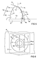
- Figure 6 is a top view of an optoelectronic package including a lens assembly.
- the optoelectronic component 2 is arranged on or in the carrier 4, and the lens or lens-shaped region 1 is arranged on or above the optoelectronic component 2.
- the upper surface 11 of the lens or lens-shaped region 1 is shown to be provided with a dimple 18.
- the lateral surface 12 of the lens or lens-shaped region 1 is axially symmetrical.
- the width of the lens or lens-shaped region 1 therefore only depends on the height above the optoelectronic component 2, but not on the lateral direction d lat .
- the width of the lens or lens-shaped region 1 decreases from a maximal width w max at the bottom surface 13 to a non-vanishing minimal width w min at the upper surface 11.
- a width of the lens or lens-shaped region 1 is always meant to be defined by the lateral surface 12 of the lens or lens-shaped region 1. If the upper surface 11 of the lens or lens-shaped region 1 is not flat, the maximal distance from the bottom surface 13 may be reached at the centre of the upper surface 11 or, if a dimple 18 is present, on a circle around the centre of the upper surface 11. In this case a width of the lens or lens-shaped region 1 is not to be measured between points lying within the upper surface 11. Hence the relevant minimal width w min shown in Figure 6 does not vary if a lateral dimension of the top of the lens or lens-shaped region 1 varies owing to a curvature of the upper surface 11 in the region above the lateral surface 12.
- the width of the lens or lens-shaped region 1 is non-vanishing, even if the upper surface 11 may have a central peak.
- the lateral width of a conical lens vanishes at the apex
- the lateral width of the lens or lens-shaped region 1 used in the lens assembly does not vanish, which makes a substantial difference.
- Figure 7 is a top view of a further optoelectronic package including a lens assembly.
- the components shown in Figure 7 that correspond to components shown in Figure 6 are designated with the same reference numerals.
- the lens or lens-shaped region 1 is not axially symmetrical. This may be desired if the field of view is not intended to be axially symmetrical either.
- the lens or lens-shaped region 1 may be a truncated elliptical cone, for example.
- the lateral surface 12 may instead be convex or concave or composed of surface areas providing discontinuous inclinations as described above.
- the lateral width measured in any fixed lateral direction decreases in the vertical direction from a maximal width at the bottom surface 13 to a non-vanishing minimal width at the upper surface 11.
- the bottom surface 13 is an ellipse.
- a lateral direction d lat of smallest width of the lens or lens-shaped region 1 and a lateral direction D lat of largest width of the lens or lens-shaped region 1 the directions corresponding to the major and minor axes of the ellipse.
- the lateral width measured in the lateral direction d lat of smallest width of the lens or lens-shaped region 1 decreases from a maximal width w max at the bottom surface 13 to a non-vanishing minimal width w min at the upper surface 11.
- the lateral width measured in the lateral direction D lat of largest width of the lens or lens-shaped region 1 decreases from a maximal width W max at the bottom surface 13 to a non-vanishing minimal width W min at the upper surface 11.
- Figure 8 shows a top view of an embodiment of the lens assembly comprising an array 19 of lenses or lens-shaped regions 1.
- a plurality of tapered lenses or lens-shaped regions 1 forming an array may thus be employed to cover a large optoelectronic component 2 or an array of optoelectronic components 2, especially if there are constraints on the height of the package.
- a tapered lens or lens-shaped region 1 can be arranged above each optoelectronic component 2 of an array of optoelectronic components 2, as shown in Figure 8 .
- groups of optoelectronic components 2 can be provided with one lens or lens-shaped region 1 of the array 19.
- a plurality of individual apertures 3 forming an array of apertures may be adapted to the upper surfaces 11 of the lenses or lens-shaped regions 1 to prevent radiation from entering the lenses or lens-shaped regions 1 through the lateral surface 12.
- Figure 9 shows a top view of a further embodiment comprising an array 19 of lenses or lens-shaped regions 1.
- the array 19 of lenses or lens-shaped regions 1 is provided for one large optoelectronic component 2.
- each optoelectronic component 2 or some of the optoelectronic components 2 may be provided with an array 19 of lenses or lens-shaped regions 1 as shown in Figure 9 .
- the array 19 of lenses can be provided with a corresponding array of individual apertures 3, in order to prevent radiation from entering the lenses or lens-shaped regions 1 through their lateral surfaces 12.
- Figure 10 is a perspective view of a lens assembly including a moulded lens.
- the lens 1 is mounted on a carrier 4 above the optoelectronic component 2, which may be integrated in the carrier 4, for example.
- a bottom portion of the lens 1 has a concave vertical curvature, while the upper portion has a convex vertical curvature.
- a bottom portion of the lens 1 may have the shape of a truncated cone, while the upper portion forms a paraboloid of revolution, for example.
- Other shapes of the lens 1, especially the shapes shown in Figures 1 to 5 may also be formed by moulding.
- Figure 10 shows the upper surface 11 of the lens 1 to be flat, but the top of the lens 1 may instead be curved, so that moulding is facilitated.
- the top of the lens 1 may especially be provided with a dimple as in the embodiments previously described. If the lens 1 is formed by moulding, a mould may be applied directly on the carrier 4, and a mould compound that is intended as the material forming the lens 1 is then filled through a runner or sprue. A sprue ridge 20 may therefore remain at the flank of the moulded lens 1, as shown in Figure 10 by way of example.
- Figure 11 is a perspective view according to Figure 10 after a partial removal of the sprue ridge 20, which may be effected by sawing, for example. A complete removal of the sprue ridge 20 may be preferred, but stubs 21 of the sprue ridge 20 may be left at the lateral surface 12 of the lens 1.
- An encasement 7 is prepared and arranged above the carrier 4 for mounting, as shown in Figure 11 .
- the encasement 7 is provided with a recess 22 in the shape of the lens 1.
- Such an encasement 7 can also be formed by moulding, in particular using an opaque material suitable to shield the intended radiation.
- the encasement 7 is put over the lens 1 and fastened on the carrier 4 by means of a suitable adhesive, for instance.
- a cover 8 as shown in Figure 1 may additionally be applied on the encasement 7.
- Figure 12 is a perspective view according to Figure 10 for an intermediate product of a variant of the method.
- the lens 1 has been embedded in a coating 23, which is provided as a sacrificial layer.
- the coating 23 can be applied by conventional dispensing or moulding, for instance.
- the lateral surface 12 of the lens 1 is preferably completely covered by the coating 23. Apart from that, the coating 23 may have any appropriate shape.
- the upper surface 11 may also be covered, or it may be free from the coating 23 as shown in Figure 12 .
- the encasement 7 may subsequently be moulded directly on the carrier 4 and the coating 23, which protects the lens 1. Only the tip of the lens 1 remains exposed, and thus the aperture 3 is formed. An opaque mold compound may be preferred for the encasement 7.
- the resulting structure is similar to the result of the method previously described, but a glueing step for mounting the encasement 7 is avoided.
- Figure 13 is a perspective view of the shape the encasement 7 takes when it is moulded on the carrier 4 comprising the lens 1 and the coating 23 according to Figure 12 .
- Figure 14 is a perspective view of an optoelectronic package comprising the lens assembly and the encasement 7 for the embodiment according to Figures 12 and 13 .
- the coating 23 comprises a material that can be removed by a suitable solvent, which does not attack the material of the lens 1, such a solvent may be applied to the exposed top surface of the coating 23, after the encasement 7 has been moulded, in order to remove the coating 23 and to form a void 10 between the lens 1 and the encasement 7.
- Bump contacts 6, which may be solder balls, for instance, can be applied on the rear side of the carrier 4 for external electric connections.
- both the transparent mould compound provided for the lens 1 and the preferably opaque mould compound provided for the encasement 7 may directly be applied onto the carrier 4, without use of a sacrificial layer like the coating 23 described above.
- the lateral surface 12 of the lens 1 can be kept at least partially free from the mould compound of the encasement 7.
- a structure of the void 10 typically resembling the void 10 shown in the cross section of Figure 1 may thus be obtained.
- An interference filter may favourably be applied to the optoelectronic component 2 to compensate for effects caused by such a void 10 being present at an area of the lateral surface 12 of the lens 1.
- the lens assembly may especially be provided by reflective surfaces to fold the path of the radiation, thus allowing the optical system to reside in a compact package, while still presenting a wide field of view.
- Nested structures multiply folding the light paths by reflection or refraction may also be applied to reduce the required dimensions of the package.
- Steep surfaces that reflect most of the light using Fresnel reflection where the light travels from a low index medium (like air, for instance) to a higher index medium (like glass or transparent or semitransparent plastic, for instance) may be particularly favourable for the described purposes.
- the efficiency of the Fresnel reflection increases as the light strikes the surface at progressively steeper glancing angles.
- the accuracy and efficiency of an optoelectronic device is enhanced by the described lens assembly. It provides a large field of view while restricting the angle of view presented to the optoelectronic component. A further benefit for the user will be the small aperture, which will be less visible than in conventional optoelectronic packages.
- the dimensions, especially the height, of the optoelectronic package using the described lens assembly are substantially reduced compared with conventional packages of ambient light sensors or the like.
- the use of an opaque mould or a metal shield as a cover eliminates the need for a rubber boot.
- the method of producing the lens assembly by moulding is appropriate for mass production and reduction of the manufacturing costs.
Landscapes
- Physics & Mathematics (AREA)
- General Physics & Mathematics (AREA)
- Spectroscopy & Molecular Physics (AREA)
- Optics & Photonics (AREA)
- Life Sciences & Earth Sciences (AREA)
- Sustainable Development (AREA)
- Led Device Packages (AREA)
Abstract
Description
- Ambient light sensors (ALS) are commonly used to control the brightness of displays, both for user comfort and for the purpose of conserving battery power in handheld devices. Customers would like the ALS to respond to light hitting the sensor aperture from a wide range of angles. At the same time, many optical sensors are prone to error when light impacts the sensor surface at large angles.
-
US 2007/0176081 A1 discloses a lens assembly for use with an ambient light sensor. The lens is arranged in an aperture of a housing to direct incident light over an area of the light sensor that is greater than the area of the housing aperture. -
US 8,319,764 B2 discloses an ambient light sensor used for a dynamical adjustment of display brightness to compensate for changes in ambient light. A wave guide is provided for improving angular response. -
US 8,378,577 B2 discloses a liquid crystal display including an electronically controlled backlight module and an ambient light sensor, which comprises a photosensitive unit and an optical sheet with a plurality of V-shaped micro structures. -
US 2014/0103816 A1 discloses an arrangement of a touchscreen glass for increasing the reception of an ambient light sensor of a mobile phone. A light uniformizing film is disposed between the touchscreen glass and an optical sensor. - It is an object of the present invention to disclose a compact optoelectronic package providing a wide field of view. It is a further object to disclose a method of producing the optoelectronic package.
This object is achieved with the lens assembly according toclaim 1, with the optoelectronic package according toclaim 11, and with the method of producing an optoelectronic package according toclaim 12. Embodiments and variants derive from the dependent claims. - The lens assembly comprises a lens or lens-shaped region, which has an upper surface, a lateral surface surrounding the lens or lens-shaped region, and a bottom surface. An optoelectronic component is arranged at or near the bottom surface, and an aperture is arranged at the upper surface, so that the lens or lens-shaped region is arranged between the optoelectronic component and the aperture. If a direction pointing from the bottom surface towards the upper surface is designated as vertical direction, and one of the directions that are orthogonal to the vertical direction is specified as the relevant lateral direction, widths of the lens or lens-shaped region are defined in this lateral direction by the lateral surface. These widths decrease in the vertical direction from a maximal width at or near the bottom surface to a non-vanishing minimal width at the upper surface.
- An embodiment of the lens assembly further comprises an opaque encasement arranged at or near at least a portion of the lateral surface.
- A further embodiment of the lens assembly comprises an encasement forming the lateral surface, and the lateral surface is reflective for radiation incident from within the lens or lens-shaped region.
- In a further embodiment of the lens assembly, an encasement is arranged adjacent to at least a portion of the lateral surface, and the encasement has an index of refraction that is smaller than the index of refraction of the lens or lens-shaped region.
- In a further embodiment of the lens assembly, the entire lens or lens-shaped region is tapered towards the aperture. This means that the widths of the lens or lens-shaped region that are measured in the same lateral direction decrease from a maximal width at the bottom surface of the lens or lens-shaped region to a non-vanishing minimal width at the upper surface of the lens or lens-shaped region, and this is true for any specified lateral direction.
- In a further embodiment of the lens assembly, the lens or lens-shaped region is not axially symmetrical.
- A further embodiment of the lens assembly comprises a dimple in the upper surface of the lens or lens-shaped region.
- In a further embodiment of the lens assembly, areas of the lateral surface of the lens or lens-shaped region join at boundaries where the inclination of the lateral surface with respect to the bottom surface is discontinuous.
- In a further embodiment of the lens assembly, the optoelectronic component is an ambient light sensor.
- In a further embodiment of the lens assembly, an array of lenses or lens-shaped regions is provided for the optoelectronic component, the lens or lens-shaped region forming part of the array. The lenses or lens-shaped regions may all be tapered and may in particular have the same shape. An array of tapered lenses or lens-shaped regions may especially be favourable if the optoelectronic component comprises an array of optoelectronic devices like photosensors, for example.
- The optoelectronic package including such a lens assembly comprises a carrier including electric interconnections. The optoelectronic component may be mounted on the carrier or integrated in the carrier.
- In an embodiment of the optoelectronic package, the carrier is a semiconductor substrate or wafer, and the optoelectronic component is integrated in the semiconductor substrate or wafer.
- In a further embodiment of the optoelectronic package, the carrier is a printed circuit board, and the optoelectronic component is mounted on the printed circuit board.
- The method of producing an optoelectronic package comprises providing a carrier including electric interconnections, arranging an optoelectronic component in or on the carrier, forming a lens or lens-shaped region or an array of lenses or lens-shaped regions and an encasement of the lens or lens-shaped region or of the array on or above the optoelectronic component, and forming an aperture of the encasement opposite the optoelectronic component. The aperture may especially be formed in a cap layer, which is mounted to the encasement.
- In a variant of the method, the encasement and the lens or lens-shaped region or the array are formed from different materials by moulding.
- In a further variant, a coating is applied to the lens or lens-shaped region after moulding. Then the encasement is formed on the carrier adjacent to the coating by moulding, and the coating is subsequently removed, thus forming a void.
- In a further variant, a lateral surface of the lens or lens-shaped region or of the array is formed by a reflective surface of the encasement.
- The following is a detailed description of examples of the lens assembly and the method of producing an optoelectronic package in conjunction with the appended figures.
- Figure 1
- is a cross section of an optoelectronic package including a lens assembly.
- Figure 2
- is a cross section of a further optoelectronic package including a lens assembly.
- Figure 3
- is a cross section of a further optoelectronic package including a tapered lens with convex sidewall.
- Figure 4
- is a cross section of a further optoelectronic package including a tapered lens with concave sidewall.
- Figure 5
- is a cross section of a further lens assembly including a lens having different bevels.
- Figure 6
- is a top view of an optoelectronic package including a lens assembly.
- Figure 7
- is a top view of a further optoelectronic package including a lens assembly.
- Figure 8
- is a top view of an optoelectronic package including a lens assembly forming an array.
- Figure 9
- is a top view of a further optoelectronic package including a lens assembly forming an array.
- Figure 10
- is a perspective view of a lens assembly including a moulded lens.
- Figure 11
- is a perspective view according to
Figure 10 with an encasement arranged for mounting. - Figure 12
- is a perspective view according to
Figure 10 after the lens has been embedded in a coating. - Figure 13
- is a perspective view of the shape of an encasement as it is moulded on the carrier.
- Figure 14
- is a perspective view of an optoelectronic package comprising the lens assembly and the encasement.
- The dimensions shown in the figures are not drawn to scale, and some aspect ratios may have been exaggerated for the sake of clarity.
-
Figure 1 is a cross section of an optoelectronic package including a lens assembly. Alens 1 formed from a transparent material or a lens-shapedregion 1, which is limited by boundary surfaces, is arranged above anoptoelectronic component 2, which may be a photodetector, for instance, or a device emitting radiation. Theoptoelectronic component 2 may especially be provided as an ambient light sensor, but other applications may be suitable as well. A surface of the lens or lens-shapedregion 1 facing theoptoelectronic component 2, which will here be designated as thebottom surface 13, may be contiguous with a surface of theoptoelectronic component 2. The lens or lens-shapedregion 1 may instead be arranged at a distance from theoptoelectronic component 2, which may be embedded in transparent material filling the interspace between theoptoelectronic component 2 and the lens or lens-shapedregion 1. At least one further optical component like an interference filter, for instance, may optionally be arranged at or on theoptoelectronic component 2.Figure 1 shows a schematic representation of theoptoelectronic component 2, which is meant to include these options. Anaperture 3 is arranged at theupper surface 11 of the lens or lens-shapedregion 1 opposite thebottom surface 13. The lens or lens-shapedregion 1 is thus arranged between theoptoelectronic component 2 and theaperture 3. - The optoelectronic package comprising the lens assembly may include a
carrier 4 with electric interconnections 5, which may be provided withbump contacts 6 or the like for external electric connection. Thecarrier 4 may be a semiconductor substrate or wafer, and theoptoelectronic component 2 may be integrated in the semiconductor substrate or wafer. In this case the interconnections 5 may form a wiring, which may also be provided for further integrated components like CMOS components, and may in particular include through-substrate vias. The interconnections 5 and integrated components may be produced in a standard CMOS process, for instance. The lens or lens-shapedregion 1 and theaperture 3 may thus be integrated at wafer level, which enables minimizing the footprint and assembly costs. Thecarrier 4 may instead be any other carrier suitable for optoelectronic packages, like a printed circuit board, for instance. Theoptoelectronic component 2 may be mounted on the printed circuit board using conventional semiconductor technology.
Anencasement 7 may be provided for the lens or lens-shapedregion 1. Theencasement 7 may be opaque, or it may by transparent, in particular comprising an index of refraction that allows total internal reflection in the lens or lens-shapedregion 1. If the lens assembly comprises alens 1 formed from a transparent material, theencasement 7 may be in contact with the entirelateral surface 12 of thelens 1, or theencasement 7 may only be contiguous with a portion of thelateral surface 12 of thelens 1, as shown inFigure 1 . Theencasement 7 may instead be arranged at a distance from thelens 1. If theencasement 7 does not cover the entirelateral surface 12 of thelens 1, a void 10, which may be filled with air, for instance, is left between theencasement 7 and thelens 1. In particular, if theencasement 7 is opaque, such avoid 10 of small index of refraction may enable the occurrence of total internal reflection in thelens 1. Thelens 1 and/or theencasement 7 can be formed by moulding, for example. - A lens-shaped
region 1 may be present instead of alens 1. The lens-shapedregion 1, which may be filled with air, for instance, can be defined by theencasement 7, which in this case provides thelateral surface 12 of the lens-shapedregion 1. Furthermore, any other suitable surface reflecting the radiation or providing a discontinuity of the index of refraction may be provided between regions of the package. In particular, thelateral surface 12 of the lens-shapedregion 1 may be provided with a reflective coating, which is not shown inFigure 1 . Surface layers that reflect the incident radiation, like aluminium coatings on plastic or glass, which may be used as the material of theencasement 7, for instance, may also be applied to fold the path of radiation. - The
aperture 3 can be formed by theencasement 7, or anoptional cap layer 8 with a window provided to form theaperture 3 can be mounted to the lens assembly. Thecap layer 8 may be opaque or semitransparent to shield stray light, and its transparency may especially depend on the wavelength. In particular, thecap layer 8 may be formed by a metal shield, for instance. - A direction pointing from the
bottom surface 13 towards theupper surface 11 will here be designated as vertical direction dv, and one of the directions that are orthogonal to the vertical direction dv is specified as the relevant lateral direction. Widths w1, w2 of the lens or lens-shapedregion 1 are defined in the specified lateral direction by thelateral surface 12.Figure 1 shows a first width w1 at a first distance d1 from thebottom surface 13 and a smaller second width w2 at a larger second distance d2 from thebottom surface 13. The widths w1, w2 thus defined decrease in the vertical direction dv from a maximal width at thebottom surface 13 to a non-vanishing minimal width at theupper surface 11. In the embodiment shown inFigure 1 , the lens or lens-shapedregion 1 especially comprises the shape of a truncated cone. Other suitable shapes will be described in the following in conjunction with various embodiments. -
Figure 2 is a cross section of a further optoelectronic package including a lens assembly. Components of the optoelectronic package according toFigure 2 that correspond to similar components of the optoelectronic package according toFigure 1 are designated with the same reference numerals. Theaperture 3 of the lens assembly shown inFigure 2 is formed by theencasement 7, which covers the entirelateral surface 12 of the lens or lens-shapedregion 1 in this embodiment. The lens or lens-shapedregion 1 can be used to direct incident radiation from a wide field of view onto theoptoelectronic component 2. In the following description, the lens assembly will be assumed to include alens 1 formed from a transparent material having an index of refraction larger than the index of refraction of air (≈1). -
Figure 2 shows aray 9 incident on theupper surface 11 of thelens 1 through theaperture 3 at an angle a1 of incidence with respect to the normal n1 to theupper surface 11. The angle a2 of refraction differs from the angle a1 of incidence according to Snell's law, taking account of the index of refraction of thelens 1. The direction of theray 9 thus deviates within thelens 1 from the direction of a virtual straight ray 9'. The refractedray 9 reaches thelateral surface 12 of thelens 1 at a further angle a3 of incidence with respect to the normal n2 to thelateral surface 12. If the index of refraction of theencasement 7 is smaller than the index of refraction of thelens 1 and the further angle a3 of incidence is sufficiently large, theray 9 is reflected by total internal reflection at thelateral surface 12 of thelens 1. The angle a3' of reflection is the same as the further angle a3 of incidence, and theray 9 is thus ultimately directed onto theoptoelectronic component 2. The original inclination of theray 9 with respect to the normal n1 is thus decreased, and the field of view of theoptoelectronic component 2 is enlarged. The direction of theray 9 may be reversed, if theoptoelectronic component 2 is a light-emitting device, for example. -
Figure 3 is a cross section of a further optoelectronic package including a lens assembly. Components of the optoelectronic package according toFigure 3 that correspond to similar components of the optoelectronic package according toFigures 1 and2 are designated with the same reference numerals. The lens assembly of the embodiment according toFigure 3 comprises a taperedlens 1 with a convex cross section of thelateral surface 12. Thelateral surface 12 is bulged in such a manner that its inclination with respect to thebottom surface 13 decreases in the vertical direction with increasing distance from thebottom surface 13. This means that, if the cross section shown inFigure 3 is at a position where thelateral surface 12 is orthogonal to the plane of the drawing, so that the normal n2 to thelateral surface 12 always lies within the cross section, the acute angle between the normal n3 to thebottom surface 13 and the normal n2 to thelateral surface 12 at a given point p of thelateral surface 12 decreases with increasing distance of the point p from thebottom surface 13. The shape of thelateral surface 12 may be selected from a variety of shapes, and its curvature can be adapted to requirements of individual applications. The curvature may be elliptical, parabolical, hyperbolical or exponential, for instance, or corresponding to any other either analytically defined or irregular geometrical shapes. - The
upper surface 11 and the portion of thelateral surface 12 that is in the vicinity of theupper surface 11 may show a pronounced deviation from the general shape of thelateral surface 12. In particular, the top of thelens 1, where radiation enters or leaves thelens 1, may be spherical, ellipsoidal or the like, irrespective of the shape of the lower portion of thelateral surface 12. - The height of the
lens 1 and its tapering may be restricted by prescribed maximal dimensions of the package and the physical width of the active area, which may cause deviations from the desired angular field of view. Such deviations can at least partially be corrected by adimple 18 formed in theupper surface 11 of thelens 1. Such adimple 18 is suitable for manufacture by moulding, which may be preferred in view of efficiency and low costs. In particular, the size of thedimple 18 and its curvature comply with requirements specified by mould manufacturers. Instead of thedimple 18, an opaque or partially opaque (i. e. translucent) ink dot placed on the tip of thelens 1 may be applied as an alternative for attenuating the radiation in the vicinity of the axis of thelens 1. -
Figure 4 is a cross section of a further optoelectronic package including a lens assembly. Components of the optoelectronic package according toFigure 4 that correspond to similar components of the optoelectronic package according toFigure 3 are designated with the same reference numerals. The lens assembly of the embodiment according toFigure 4 comprises a taperedlens 1 with a concave cross section of thelateral surface 12. Thelateral surface 12 is curved in such a manner that its inclination with respect to thebottom surface 13 increases in the vertical direction with increasing distance from thebottom surface 13. This means that, if the cross section shown inFigure 4 is at a position where thelateral surface 12 is orthogonal to the plane of the drawing, so that the normal n2 to thelateral surface 12 always lies within the cross section, the acute angle between the normal n3 to thebottom surface 13 and the normal n2 to thelateral surface 12 at a given point p of thelateral surface 12 increases with increasing distance of the point p from thebottom surface 13. - In the embodiment according to
Figure 4 , as in the embodiment according toFigure 3 , the shape of thelateral surface 12 may be selected from a variety of shapes, and its curvature can be adapted to requirements of individual applications. The curvature may be elliptical, parabolical, hyperbolical or exponential, for instance, or corresponding to any other either analytically defined or irregular geometrical shapes. In other embodiments of thelens 1, the vertical curvature may be partially convex and partially concave. - In
Figures 3 and 4 the curvature of thelateral surface 12 is clearly indicated. But in preferred embodiments of the lens assembly, the vertical curvature of thelens 1 may typically be weaker than shown in the figures, so that the shape of thelateral surface 12 does not deviate significantly from a cone. The top of thelens 1 including theupper surface 11 may deviate from the general shape of thelens 1 and may especially be spherical or ellipsoidal, irrespective of the shape of the lower portion of thelateral surface 12. - If the height of the
lens 1 and its tapering is restricted by prescribed requirements, adimple 18 can be provided in theupper surface 11 of thelens 1 as described above in conjunction with the embodiment according toFigure 3 . Such adimple 18 can also be provided in theupper surface 11 of thelens 1 of any other embodiment, in particular in theupper surface 11 of alens 1 forming a truncated cone, as in the embodiments according toFigures 1 and2 . -
Figure 5 is a cross section of a further lens assembly including a lens having different bevels. Thelateral surface 12 is formed bylateral surface areas lateral surface areas lens 1, in particular a vertical convex or concave curvature. InFigure 5 , by way of example, thelateral surface areas lateral surface areas bottom surface 13 are shown inFigure 5 by means of broken lines extending the cross sections of the upperlateral surface area 14 and the middlelateral surface area 15. The angle a4 of inclination of the upperlateral surface area 14 is smaller than the angle a5 of inclination of the middlelateral surface area 15, and the latter angle a5 is smaller than the angle a6 of inclination of the lowerlateral surface area 16. Thelateral surface areas boundaries 17 where the angles a4, a5, a6 of inclination vary discontinuously. -
Figure 5 shows how aconvex lens 1, especially alens 1 having different bevels, may be used for the direction of aray 9 by means of repeated total internal reflection. Theincident ray 9 is refracted at theupper surface 11 of thelens 1 and totally internally reflected at the upperlateral surface area 14. As the upperlateral surface area 14 and the middlelateral surface area 15 comprise normals n4, n5 that are not parallel to one another, the reflectedray 9 may impinge on the middlelateral surface area 15 and again be reflected by total internal reflection. As the middlelateral surface area 15 and the lowerlateral surface area 16 comprise normals n5, n6 that are not parallel either, the twice reflectedray 9 may also impinge on the lowerlateral surface area 16 and again be reflected by total internal reflection. The total angle of deflection of theray 9 thus achieved is essentially larger than the angle of deflection in the case of only one total internal reflection.Figure 5 also shows how the succession of different angles a4, a5, a6 of inclination of thelateral surface 12 causes a corresponding succession of angles of incidence sufficiently large for total internal reflection of theray 9. -
Figure 6 is a top view of an optoelectronic package including a lens assembly. Theoptoelectronic component 2 is arranged on or in thecarrier 4, and the lens or lens-shapedregion 1 is arranged on or above theoptoelectronic component 2. Theupper surface 11 of the lens or lens-shapedregion 1 is shown to be provided with adimple 18. In the embodiment shown inFigure 6 , thelateral surface 12 of the lens or lens-shapedregion 1 is axially symmetrical. The width of the lens or lens-shapedregion 1 therefore only depends on the height above theoptoelectronic component 2, but not on the lateral direction dlat. The width of the lens or lens-shapedregion 1 decreases from a maximal width wmax at thebottom surface 13 to a non-vanishing minimal width wmin at theupper surface 11. - In this description and in the claims, a width of the lens or lens-shaped
region 1 is always meant to be defined by thelateral surface 12 of the lens or lens-shapedregion 1. If theupper surface 11 of the lens or lens-shapedregion 1 is not flat, the maximal distance from thebottom surface 13 may be reached at the centre of theupper surface 11 or, if adimple 18 is present, on a circle around the centre of theupper surface 11. In this case a width of the lens or lens-shapedregion 1 is not to be measured between points lying within theupper surface 11. Hence the relevant minimal width wmin shown inFigure 6 does not vary if a lateral dimension of the top of the lens or lens-shapedregion 1 varies owing to a curvature of theupper surface 11 in the region above thelateral surface 12. In this sense the width of the lens or lens-shapedregion 1 is non-vanishing, even if theupper surface 11 may have a central peak. Whereas the lateral width of a conical lens vanishes at the apex, the lateral width of the lens or lens-shapedregion 1 used in the lens assembly does not vanish, which makes a substantial difference. -
Figure 7 is a top view of a further optoelectronic package including a lens assembly. The components shown inFigure 7 that correspond to components shown inFigure 6 are designated with the same reference numerals. In the embodiment shown inFigure 7 , the lens or lens-shapedregion 1 is not axially symmetrical. This may be desired if the field of view is not intended to be axially symmetrical either. The lens or lens-shapedregion 1 may be a truncated elliptical cone, for example. Thelateral surface 12 may instead be convex or concave or composed of surface areas providing discontinuous inclinations as described above. The lateral width measured in any fixed lateral direction decreases in the vertical direction from a maximal width at thebottom surface 13 to a non-vanishing minimal width at theupper surface 11. - In the embodiment according to
Figure 7 , thebottom surface 13 is an ellipse. In the case of a lens or lens-shapedregion 1 forming an elliptical cone, at any fixed distance from thebottom surface 13, there is a lateral direction dlat of smallest width of the lens or lens-shapedregion 1 and a lateral direction Dlat of largest width of the lens or lens-shapedregion 1, the directions corresponding to the major and minor axes of the ellipse. The lateral width measured in the lateral direction dlat of smallest width of the lens or lens-shapedregion 1 decreases from a maximal width wmax at thebottom surface 13 to a non-vanishing minimal width wmin at theupper surface 11. In the same way, the lateral width measured in the lateral direction Dlat of largest width of the lens or lens-shapedregion 1 decreases from a maximal width Wmax at thebottom surface 13 to a non-vanishing minimal width Wmin at theupper surface 11. -
Figure 8 shows a top view of an embodiment of the lens assembly comprising anarray 19 of lenses or lens-shapedregions 1. A plurality of tapered lenses or lens-shapedregions 1 forming an array may thus be employed to cover a largeoptoelectronic component 2 or an array ofoptoelectronic components 2, especially if there are constraints on the height of the package. A tapered lens or lens-shapedregion 1 can be arranged above eachoptoelectronic component 2 of an array ofoptoelectronic components 2, as shown inFigure 8 . Instead, groups ofoptoelectronic components 2 can be provided with one lens or lens-shapedregion 1 of thearray 19. A plurality ofindividual apertures 3 forming an array of apertures may be adapted to theupper surfaces 11 of the lenses or lens-shapedregions 1 to prevent radiation from entering the lenses or lens-shapedregions 1 through thelateral surface 12. -
Figure 9 shows a top view of a further embodiment comprising anarray 19 of lenses or lens-shapedregions 1. In the embodiment according toFigure 9 , thearray 19 of lenses or lens-shapedregions 1 is provided for one largeoptoelectronic component 2. In an array ofoptoelectronic components 2, eachoptoelectronic component 2 or some of theoptoelectronic components 2 may be provided with anarray 19 of lenses or lens-shapedregions 1 as shown inFigure 9 . Thearray 19 of lenses can be provided with a corresponding array ofindividual apertures 3, in order to prevent radiation from entering the lenses or lens-shapedregions 1 through their lateral surfaces 12. -
Figure 10 is a perspective view of a lens assembly including a moulded lens. Thelens 1 is mounted on acarrier 4 above theoptoelectronic component 2, which may be integrated in thecarrier 4, for example. In the embodiment according toFigure 10 , a bottom portion of thelens 1 has a concave vertical curvature, while the upper portion has a convex vertical curvature. Instead, a bottom portion of thelens 1 may have the shape of a truncated cone, while the upper portion forms a paraboloid of revolution, for example. Other shapes of thelens 1, especially the shapes shown inFigures 1 to 5 , may also be formed by moulding.Figure 10 shows theupper surface 11 of thelens 1 to be flat, but the top of thelens 1 may instead be curved, so that moulding is facilitated. The top of thelens 1 may especially be provided with a dimple as in the embodiments previously described. If thelens 1 is formed by moulding, a mould may be applied directly on thecarrier 4, and a mould compound that is intended as the material forming thelens 1 is then filled through a runner or sprue. Asprue ridge 20 may therefore remain at the flank of the mouldedlens 1, as shown inFigure 10 by way of example. -
Figure 11 is a perspective view according toFigure 10 after a partial removal of thesprue ridge 20, which may be effected by sawing, for example. A complete removal of thesprue ridge 20 may be preferred, but stubs 21 of thesprue ridge 20 may be left at thelateral surface 12 of thelens 1. Anencasement 7 is prepared and arranged above thecarrier 4 for mounting, as shown inFigure 11 . Theencasement 7 is provided with arecess 22 in the shape of thelens 1. Such anencasement 7 can also be formed by moulding, in particular using an opaque material suitable to shield the intended radiation. As indicated inFigure 11 by arrows, theencasement 7 is put over thelens 1 and fastened on thecarrier 4 by means of a suitable adhesive, for instance. Acover 8 as shown inFigure 1 may additionally be applied on theencasement 7. -
Figure 12 is a perspective view according toFigure 10 for an intermediate product of a variant of the method. Thelens 1 has been embedded in acoating 23, which is provided as a sacrificial layer. Thecoating 23 can be applied by conventional dispensing or moulding, for instance. Thelateral surface 12 of thelens 1 is preferably completely covered by thecoating 23. Apart from that, thecoating 23 may have any appropriate shape. Theupper surface 11 may also be covered, or it may be free from thecoating 23 as shown inFigure 12 . Theencasement 7 may subsequently be moulded directly on thecarrier 4 and thecoating 23, which protects thelens 1. Only the tip of thelens 1 remains exposed, and thus theaperture 3 is formed. An opaque mold compound may be preferred for theencasement 7. The resulting structure is similar to the result of the method previously described, but a glueing step for mounting theencasement 7 is avoided. -
Figure 13 is a perspective view of the shape theencasement 7 takes when it is moulded on thecarrier 4 comprising thelens 1 and thecoating 23 according toFigure 12 .
Figure 14 is a perspective view of an optoelectronic package comprising the lens assembly and theencasement 7 for the embodiment according toFigures 12 and 13 . If thecoating 23 comprises a material that can be removed by a suitable solvent, which does not attack the material of thelens 1, such a solvent may be applied to the exposed top surface of thecoating 23, after theencasement 7 has been moulded, in order to remove thecoating 23 and to form a void 10 between thelens 1 and theencasement 7. The resulting structure is similar to the embodiments shown inFigures 1 ,3 and 4 .Bump contacts 6, which may be solder balls, for instance, can be applied on the rear side of thecarrier 4 for external electric connections. - Instead of the described method, both the transparent mould compound provided for the
lens 1 and the preferably opaque mould compound provided for theencasement 7 may directly be applied onto thecarrier 4, without use of a sacrificial layer like thecoating 23 described above. Furthermore, by using an appropriate mould for theencasement 7, thelateral surface 12 of thelens 1 can be kept at least partially free from the mould compound of theencasement 7. A structure of the void 10 typically resembling the void 10 shown in the cross section ofFigure 1 , by way of example, may thus be obtained. An interference filter may favourably be applied to theoptoelectronic component 2 to compensate for effects caused by such a void 10 being present at an area of thelateral surface 12 of thelens 1. - The lens assembly may especially be provided by reflective surfaces to fold the path of the radiation, thus allowing the optical system to reside in a compact package, while still presenting a wide field of view. Nested structures multiply folding the light paths by reflection or refraction may also be applied to reduce the required dimensions of the package. Steep surfaces that reflect most of the light using Fresnel reflection, where the light travels from a low index medium (like air, for instance) to a higher index medium (like glass or transparent or semitransparent plastic, for instance) may be particularly favourable for the described purposes. The efficiency of the Fresnel reflection increases as the light strikes the surface at progressively steeper glancing angles.
- The accuracy and efficiency of an optoelectronic device is enhanced by the described lens assembly. It provides a large field of view while restricting the angle of view presented to the optoelectronic component. A further benefit for the user will be the small aperture, which will be less visible than in conventional optoelectronic packages. The dimensions, especially the height, of the optoelectronic package using the described lens assembly are substantially reduced compared with conventional packages of ambient light sensors or the like. The use of an opaque mould or a metal shield as a cover eliminates the need for a rubber boot. The method of producing the lens assembly by moulding is appropriate for mass production and reduction of the manufacturing costs.
-
- 1
- lens or lens-shaped region
- 2
- optoelectronic component
- 3
- aperture
- 4
- carrier
- 5
- interconnection
- 6
- bump contact
- 7
- encasement
- 8
- cap layer
- 9
- ray
- 9'
- virtual ray
- 10
- void
- 11
- upper surface
- 12
- lateral surface
- 13
- bottom surface
- 14
- upper lateral surface area
- 15
- middle lateral surface area
- 16
- lower lateral surface area
- 17
- boundary
- 18
- dimple
- 19
- array of lenses
- 20
- sprue ridge
- 21
- stub
- 22
- recess
- 23
- coating
- a1
- angle of incidence
- a2
- angle of refraction
- a3
- further angle of incidence
- a3'
- angle of reflection
- a4
- angle of inclination of the upper lateral surface area
- a5
- angle of inclination of the middle lateral surface area
- a6
- angle of inclination of the lower lateral surface area
- d1
- first distance
- d2
- second distance
- dlat
- lateral direction of smallest widths
- Dlat
- lateral direction of largest widths
- dv
- vertical direction
- n1
- normal to the upper surface
- n2
- normal to the lateral surface
- n3
- normal to the bottom surface
- n4
- normal to the upper lateral surface area
- n5
- normal to the middle lateral surface area
- n6
- normal to the lower lateral surface area
- w1
- first width
- w2
- second width
- wmax
- smallest maximal width
- Wmax
- largest maximal width
- wmin
- smallest minimal width
- Wmin
- largest minimal width
Claims (15)
- A lens assembly, comprising:- a lens or lens-shaped region (1), which has an upper surface (11), a lateral surface (12) surrounding the lens or lens-shaped region (1), and a bottom surface (13),- a lateral direction (dlat, Dlat), which is orthogonal to a vertical direction (dv) pointing from the bottom surface (13) towards the upper surface (11),- an optoelectronic component (2) arranged at or near the bottom surface (13), and- an aperture (3) at the upper surface (11), the lens or lens-shaped region (1) being arranged between the optoelectronic component (2) and the aperture (3),characterized in that- widths (w1, w2) of the lens or lens-shaped region (1) that are defined in the lateral direction (dlat, Dlat) by the lateral surface (12) decrease in the vertical direction (dv) from a maximal width (wmax, Wmax) at or near the bottom surface (13) to a non-vanishing minimal width (wmin, Wmin) at the upper surface (11).
- The lens assembly of claim 1, further comprising:an opaque encasement (7) arranged at or near at least a portion of the lateral surface (12).
- The lens assembly of claim 1, further comprising:an encasement (7) forming the lateral surface (12), and the lateral surface (12) being reflective for radiation incident from within the lens or lens-shaped region (1).
- The lens assembly of claim 1, further comprising:an index of refraction of the lens or lens-shaped region (1), andan encasement (7) having a smaller index of refraction being arranged adjacent to at least a portion of the lateral surface (12).
- The lens assembly of one of claims 1 to 4, wherein
the entire lens or lens-shaped region (1) is tapered towards the aperture (3). - The lens assembly of one of claims 1 to 5, wherein
the lens or lens-shaped region (1) is not axially symmetrical. - The lens assembly of one of claims 1 to 6, further comprising:a dimple (18) formed in the upper surface (11).
- The lens assembly of one of claims 1 to 7, wherein areas (14, 15, 16) of the lateral surface (12) of the lens or lens-shaped region (1) join at boundaries (17) where an inclination (a4, a5, a6) of the lateral surface (12) with respect to the bottom surface (13) is discontinuous.
- The lens assembly of one of claims 1 to 8, wherein the optoelectronic component (2) is an ambient light sensor.
- The lens assembly of one of claims 1 to 9, further comprising:an array (19) of lenses or lens-shaped regions provided for the optoelectronic component (2), the lens or lens-shaped region (1) forming part of the array (19).
- An optoelectronic package including a lens assembly of one of claims 1 to 10, comprising:a carrier (4) including electric interconnections (5),the optoelectronic component (2) being mounted on the carrier (4) or integrated in the carrier (4).
- A method of producing an optoelectronic package, comprising:- providing a carrier (4) including electric interconnections (5),- arranging an optoelectronic component (2) in or on the carrier (4),- forming a lens or lens-shaped region (1) or an array (19) of lenses or lens-shaped regions and an encasement (7) of the lens or lens-shaped region (1) or of the array (19) on or above the optoelectronic component (2), and- forming an aperture (3) of the encasement (7) opposite the optoelectronic component (2).
- The method of producing an optoelectronic package according to claim 12, further comprising:forming the encasement (7) and the lens or lens-shaped region (1) or the array (19) from different materials by moulding.
- The method of producing an optoelectronic package according to claim 13, further comprising:after moulding the lens or lens-shaped region (1),applying a coating (23),moulding the encasement (7) on the carrier (4) adjacent to the coating (23), andsubsequently removing the coating (23), thus forming a void (10).
- The method of producing an optoelectronic package according to one of claims 12 to 14, further comprising:forming a lateral surface (12) of the lens or lens-shaped region (1) or of the array (19) by a reflective surface of the encasement (7).
Priority Applications (1)
| Application Number | Priority Date | Filing Date | Title |
|---|---|---|---|
| PCT/EP2015/061723 WO2016005097A1 (en) | 2014-07-09 | 2015-05-27 | Lens assembly, optoelectronic package and method of producing an optoelectronic package with lens assembly |
Applications Claiming Priority (1)
| Application Number | Priority Date | Filing Date | Title |
|---|---|---|---|
| US201462022529P | 2014-07-09 | 2014-07-09 |
Publications (2)
| Publication Number | Publication Date |
|---|---|
| EP2966491A1 true EP2966491A1 (en) | 2016-01-13 |
| EP2966491B1 EP2966491B1 (en) | 2022-02-02 |
Family
ID=51625867
Family Applications (1)
| Application Number | Title | Priority Date | Filing Date |
|---|---|---|---|
| EP14186386.0A Active EP2966491B1 (en) | 2014-07-09 | 2014-09-25 | Lens assembly, optoelectronic package and method of producing an optoelectronic package with lens assembly |
Country Status (2)
| Country | Link |
|---|---|
| EP (1) | EP2966491B1 (en) |
| WO (1) | WO2016005097A1 (en) |
Cited By (1)
| Publication number | Priority date | Publication date | Assignee | Title |
|---|---|---|---|---|
| EP3166146A1 (en) * | 2015-11-06 | 2017-05-10 | ams AG | Optical package and method of producing an optical package |
Families Citing this family (1)
| Publication number | Priority date | Publication date | Assignee | Title |
|---|---|---|---|---|
| EP3242114B1 (en) | 2016-05-04 | 2019-05-01 | ams AG | Arrangement of an aperture and a filter region for a filter sensor device and filter sensor device |
Citations (9)
| Publication number | Priority date | Publication date | Assignee | Title |
|---|---|---|---|---|
| WO1996031742A1 (en) * | 1995-04-07 | 1996-10-10 | Tir Technologies, Inc. | Collimating tir lens devices employing fluorescent light sources |
| FR2887627A1 (en) * | 2005-06-28 | 2006-12-29 | Sagem Defense Securite | INFRARED RADIATION DETECTING APPARATUS, COMPRISING A COLD SCREEN WITH ELLIPTICAL SECTION |
| US20070176081A1 (en) | 2006-02-01 | 2007-08-02 | Stricklin Robert S | Lens for Ambient Light Sensor |
| US20120037205A1 (en) * | 2010-08-16 | 2012-02-16 | Saied Tadayon | Solar Cell Concentrator |
| US20120037793A1 (en) * | 2010-08-10 | 2012-02-16 | Chi Boon Ong | Lens having multiple conic sections for leds and proximity sensors |
| US8319764B2 (en) | 2009-06-29 | 2012-11-27 | Research In Motion Limited | Wave guide for improving light sensor angular response |
| US8378577B2 (en) | 2009-12-30 | 2013-02-19 | Hon Hai Precision Industry Co., Ltd. | Liquid crystal display with ambient light sensor |
| US20140103816A1 (en) | 2012-10-15 | 2014-04-17 | Huawei Device Co., Ltd | Method and Structure for Increasing Receiving Angle of Optical Sensor and Handheld Terminal |
| US20140145069A1 (en) * | 2012-11-28 | 2014-05-29 | Intersil Americas LLC | Packaged light detector semiconductor devices with non-imaging optics for ambient light and/or optical proxmity sensing, methods for manufacturing the same, and systems including the same |
Family Cites Families (1)
| Publication number | Priority date | Publication date | Assignee | Title |
|---|---|---|---|---|
| JP6003121B2 (en) * | 2012-03-15 | 2016-10-05 | オムロン株式会社 | Reflective photoelectric sensor |
-
2014
- 2014-09-25 EP EP14186386.0A patent/EP2966491B1/en active Active
-
2015
- 2015-05-27 WO PCT/EP2015/061723 patent/WO2016005097A1/en not_active Ceased
Patent Citations (9)
| Publication number | Priority date | Publication date | Assignee | Title |
|---|---|---|---|---|
| WO1996031742A1 (en) * | 1995-04-07 | 1996-10-10 | Tir Technologies, Inc. | Collimating tir lens devices employing fluorescent light sources |
| FR2887627A1 (en) * | 2005-06-28 | 2006-12-29 | Sagem Defense Securite | INFRARED RADIATION DETECTING APPARATUS, COMPRISING A COLD SCREEN WITH ELLIPTICAL SECTION |
| US20070176081A1 (en) | 2006-02-01 | 2007-08-02 | Stricklin Robert S | Lens for Ambient Light Sensor |
| US8319764B2 (en) | 2009-06-29 | 2012-11-27 | Research In Motion Limited | Wave guide for improving light sensor angular response |
| US8378577B2 (en) | 2009-12-30 | 2013-02-19 | Hon Hai Precision Industry Co., Ltd. | Liquid crystal display with ambient light sensor |
| US20120037793A1 (en) * | 2010-08-10 | 2012-02-16 | Chi Boon Ong | Lens having multiple conic sections for leds and proximity sensors |
| US20120037205A1 (en) * | 2010-08-16 | 2012-02-16 | Saied Tadayon | Solar Cell Concentrator |
| US20140103816A1 (en) | 2012-10-15 | 2014-04-17 | Huawei Device Co., Ltd | Method and Structure for Increasing Receiving Angle of Optical Sensor and Handheld Terminal |
| US20140145069A1 (en) * | 2012-11-28 | 2014-05-29 | Intersil Americas LLC | Packaged light detector semiconductor devices with non-imaging optics for ambient light and/or optical proxmity sensing, methods for manufacturing the same, and systems including the same |
Cited By (3)
| Publication number | Priority date | Publication date | Assignee | Title |
|---|---|---|---|---|
| EP3166146A1 (en) * | 2015-11-06 | 2017-05-10 | ams AG | Optical package and method of producing an optical package |
| WO2017077051A1 (en) * | 2015-11-06 | 2017-05-11 | Ams Ag | Optical package and method of producing an optical package |
| US10847664B2 (en) | 2015-11-06 | 2020-11-24 | Ams Ag | Optical package and method of producing an optical package |
Also Published As
| Publication number | Publication date |
|---|---|
| WO2016005097A1 (en) | 2016-01-14 |
| EP2966491B1 (en) | 2022-02-02 |
Similar Documents
| Publication | Publication Date | Title |
|---|---|---|
| KR100616598B1 (en) | Light emitting diode lens and backlight module having the same | |
| KR100436302B1 (en) | Optical Device for an Optical Element and Apparatus Employing the Device | |
| US20090045421A1 (en) | Surface mount type light emitting diode package device | |
| CN111448652B (en) | A display capable of detecting fingerprints | |
| CN114520281B (en) | Light-emitting device, backlight plate and display panel | |
| US9356185B2 (en) | Compact light sensing modules including reflective surfaces to enhance light collection and/or emission, and methods of fabricating such modules | |
| CN113050326A (en) | Lamp panel and backlight module | |
| WO2021035714A1 (en) | Texture image acquisition device, display device, and collimation component | |
| US10847664B2 (en) | Optical package and method of producing an optical package | |
| CN110706609A (en) | Display modules and electronic devices | |
| CN114730851A (en) | Lighting device comprising passive optical nanostructures | |
| US11437447B2 (en) | Display device and manufacturing method thereof | |
| CN205121507U (en) | Touch control display equipment | |
| CN111564519A (en) | Proximity Sensors and Electronic Machines Using The Same | |
| WO2020168953A1 (en) | Screen assembly and electronic device | |
| WO2022252269A1 (en) | Cover plate and display apparatus | |
| CN209859155U (en) | Fingerprint identification device and electronic equipment | |
| EP2966491B1 (en) | Lens assembly, optoelectronic package and method of producing an optoelectronic package with lens assembly | |
| CN113325503A (en) | Diffractive optical element and optical apparatus | |
| US20070217195A1 (en) | Light-emitting device and a lens thereof | |
| CN109742097B (en) | Display device | |
| CN209543378U (en) | Screen components and electronic equipment | |
| US12604590B2 (en) | Light emitting module and display device comprising reflective layer surrounding the light emitting units | |
| CN102841393A (en) | Reflective sheet and optical touch device of the reflective sheet | |
| CN224218751U (en) | Optical sensor and electronic device |
Legal Events
| Date | Code | Title | Description |
|---|---|---|---|
| PUAI | Public reference made under article 153(3) epc to a published international application that has entered the european phase |
Free format text: ORIGINAL CODE: 0009012 |
|
| AK | Designated contracting states |
Kind code of ref document: A1 Designated state(s): AL AT BE BG CH CY CZ DE DK EE ES FI FR GB GR HR HU IE IS IT LI LT LU LV MC MK MT NL NO PL PT RO RS SE SI SK SM TR |
|
| AX | Request for extension of the european patent |
Extension state: BA ME |
|
| 17P | Request for examination filed |
Effective date: 20160413 |
|
| RBV | Designated contracting states (corrected) |
Designated state(s): AL AT BE BG CH CY CZ DE DK EE ES FI FR GB GR HR HU IE IS IT LI LT LU LV MC MK MT NL NO PL PT RO RS SE SI SK SM TR |
|
| RAP1 | Party data changed (applicant data changed or rights of an application transferred) |
Owner name: AMS AG |
|
| STAA | Information on the status of an ep patent application or granted ep patent |
Free format text: STATUS: EXAMINATION IS IN PROGRESS |
|
| 17Q | First examination report despatched |
Effective date: 20190320 |
|
| GRAP | Despatch of communication of intention to grant a patent |
Free format text: ORIGINAL CODE: EPIDOSNIGR1 |
|
| STAA | Information on the status of an ep patent application or granted ep patent |
Free format text: STATUS: GRANT OF PATENT IS INTENDED |
|
| INTG | Intention to grant announced |
Effective date: 20210716 |
|
| GRAS | Grant fee paid |
Free format text: ORIGINAL CODE: EPIDOSNIGR3 |
|
| GRAJ | Information related to disapproval of communication of intention to grant by the applicant or resumption of examination proceedings by the epo deleted |
Free format text: ORIGINAL CODE: EPIDOSDIGR1 |
|
| GRAL | Information related to payment of fee for publishing/printing deleted |
Free format text: ORIGINAL CODE: EPIDOSDIGR3 |
|
| STAA | Information on the status of an ep patent application or granted ep patent |
Free format text: STATUS: EXAMINATION IS IN PROGRESS |
|
| GRAP | Despatch of communication of intention to grant a patent |
Free format text: ORIGINAL CODE: EPIDOSNIGR1 |
|
| STAA | Information on the status of an ep patent application or granted ep patent |
Free format text: STATUS: GRANT OF PATENT IS INTENDED |
|
| INTC | Intention to grant announced (deleted) | ||
| INTG | Intention to grant announced |
Effective date: 20211129 |
|
| GRAA | (expected) grant |
Free format text: ORIGINAL CODE: 0009210 |
|
| STAA | Information on the status of an ep patent application or granted ep patent |
Free format text: STATUS: THE PATENT HAS BEEN GRANTED |
|
| AK | Designated contracting states |
Kind code of ref document: B1 Designated state(s): AL AT BE BG CH CY CZ DE DK EE ES FI FR GB GR HR HU IE IS IT LI LT LU LV MC MK MT NL NO PL PT RO RS SE SI SK SM TR |
|
| REG | Reference to a national code |
Ref country code: GB Ref legal event code: FG4D |
|
| REG | Reference to a national code |
Ref country code: CH Ref legal event code: EP Ref country code: AT Ref legal event code: REF Ref document number: 1466734 Country of ref document: AT Kind code of ref document: T Effective date: 20220215 |
|
| REG | Reference to a national code |
Ref country code: DE Ref legal event code: R096 Ref document number: 602014082385 Country of ref document: DE |
|
| REG | Reference to a national code |
Ref country code: IE Ref legal event code: FG4D |
|
| REG | Reference to a national code |
Ref country code: LT Ref legal event code: MG9D |
|
| REG | Reference to a national code |
Ref country code: NL Ref legal event code: MP Effective date: 20220202 |
|
| REG | Reference to a national code |
Ref country code: AT Ref legal event code: MK05 Ref document number: 1466734 Country of ref document: AT Kind code of ref document: T Effective date: 20220202 |
|
| PG25 | Lapsed in a contracting state [announced via postgrant information from national office to epo] |
Ref country code: SE Free format text: LAPSE BECAUSE OF FAILURE TO SUBMIT A TRANSLATION OF THE DESCRIPTION OR TO PAY THE FEE WITHIN THE PRESCRIBED TIME-LIMIT Effective date: 20220202 Ref country code: RS Free format text: LAPSE BECAUSE OF FAILURE TO SUBMIT A TRANSLATION OF THE DESCRIPTION OR TO PAY THE FEE WITHIN THE PRESCRIBED TIME-LIMIT Effective date: 20220202 Ref country code: PT Free format text: LAPSE BECAUSE OF FAILURE TO SUBMIT A TRANSLATION OF THE DESCRIPTION OR TO PAY THE FEE WITHIN THE PRESCRIBED TIME-LIMIT Effective date: 20220602 Ref country code: NO Free format text: LAPSE BECAUSE OF FAILURE TO SUBMIT A TRANSLATION OF THE DESCRIPTION OR TO PAY THE FEE WITHIN THE PRESCRIBED TIME-LIMIT Effective date: 20220502 Ref country code: NL Free format text: LAPSE BECAUSE OF FAILURE TO SUBMIT A TRANSLATION OF THE DESCRIPTION OR TO PAY THE FEE WITHIN THE PRESCRIBED TIME-LIMIT Effective date: 20220202 Ref country code: LT Free format text: LAPSE BECAUSE OF FAILURE TO SUBMIT A TRANSLATION OF THE DESCRIPTION OR TO PAY THE FEE WITHIN THE PRESCRIBED TIME-LIMIT Effective date: 20220202 Ref country code: HR Free format text: LAPSE BECAUSE OF FAILURE TO SUBMIT A TRANSLATION OF THE DESCRIPTION OR TO PAY THE FEE WITHIN THE PRESCRIBED TIME-LIMIT Effective date: 20220202 Ref country code: ES Free format text: LAPSE BECAUSE OF FAILURE TO SUBMIT A TRANSLATION OF THE DESCRIPTION OR TO PAY THE FEE WITHIN THE PRESCRIBED TIME-LIMIT Effective date: 20220202 Ref country code: BG Free format text: LAPSE BECAUSE OF FAILURE TO SUBMIT A TRANSLATION OF THE DESCRIPTION OR TO PAY THE FEE WITHIN THE PRESCRIBED TIME-LIMIT Effective date: 20220502 |
|
| PG25 | Lapsed in a contracting state [announced via postgrant information from national office to epo] |
Ref country code: PL Free format text: LAPSE BECAUSE OF FAILURE TO SUBMIT A TRANSLATION OF THE DESCRIPTION OR TO PAY THE FEE WITHIN THE PRESCRIBED TIME-LIMIT Effective date: 20220202 Ref country code: LV Free format text: LAPSE BECAUSE OF FAILURE TO SUBMIT A TRANSLATION OF THE DESCRIPTION OR TO PAY THE FEE WITHIN THE PRESCRIBED TIME-LIMIT Effective date: 20220202 Ref country code: GR Free format text: LAPSE BECAUSE OF FAILURE TO SUBMIT A TRANSLATION OF THE DESCRIPTION OR TO PAY THE FEE WITHIN THE PRESCRIBED TIME-LIMIT Effective date: 20220503 Ref country code: FI Free format text: LAPSE BECAUSE OF FAILURE TO SUBMIT A TRANSLATION OF THE DESCRIPTION OR TO PAY THE FEE WITHIN THE PRESCRIBED TIME-LIMIT Effective date: 20220202 Ref country code: AT Free format text: LAPSE BECAUSE OF FAILURE TO SUBMIT A TRANSLATION OF THE DESCRIPTION OR TO PAY THE FEE WITHIN THE PRESCRIBED TIME-LIMIT Effective date: 20220202 |
|
| PG25 | Lapsed in a contracting state [announced via postgrant information from national office to epo] |
Ref country code: IS Free format text: LAPSE BECAUSE OF FAILURE TO SUBMIT A TRANSLATION OF THE DESCRIPTION OR TO PAY THE FEE WITHIN THE PRESCRIBED TIME-LIMIT Effective date: 20220602 |
|
| PG25 | Lapsed in a contracting state [announced via postgrant information from national office to epo] |
Ref country code: SM Free format text: LAPSE BECAUSE OF FAILURE TO SUBMIT A TRANSLATION OF THE DESCRIPTION OR TO PAY THE FEE WITHIN THE PRESCRIBED TIME-LIMIT Effective date: 20220202 Ref country code: SK Free format text: LAPSE BECAUSE OF FAILURE TO SUBMIT A TRANSLATION OF THE DESCRIPTION OR TO PAY THE FEE WITHIN THE PRESCRIBED TIME-LIMIT Effective date: 20220202 Ref country code: RO Free format text: LAPSE BECAUSE OF FAILURE TO SUBMIT A TRANSLATION OF THE DESCRIPTION OR TO PAY THE FEE WITHIN THE PRESCRIBED TIME-LIMIT Effective date: 20220202 Ref country code: EE Free format text: LAPSE BECAUSE OF FAILURE TO SUBMIT A TRANSLATION OF THE DESCRIPTION OR TO PAY THE FEE WITHIN THE PRESCRIBED TIME-LIMIT Effective date: 20220202 Ref country code: DK Free format text: LAPSE BECAUSE OF FAILURE TO SUBMIT A TRANSLATION OF THE DESCRIPTION OR TO PAY THE FEE WITHIN THE PRESCRIBED TIME-LIMIT Effective date: 20220202 Ref country code: CZ Free format text: LAPSE BECAUSE OF FAILURE TO SUBMIT A TRANSLATION OF THE DESCRIPTION OR TO PAY THE FEE WITHIN THE PRESCRIBED TIME-LIMIT Effective date: 20220202 |
|
| REG | Reference to a national code |
Ref country code: DE Ref legal event code: R097 Ref document number: 602014082385 Country of ref document: DE |
|
| PG25 | Lapsed in a contracting state [announced via postgrant information from national office to epo] |
Ref country code: AL Free format text: LAPSE BECAUSE OF FAILURE TO SUBMIT A TRANSLATION OF THE DESCRIPTION OR TO PAY THE FEE WITHIN THE PRESCRIBED TIME-LIMIT Effective date: 20220202 |
|
| PLBE | No opposition filed within time limit |
Free format text: ORIGINAL CODE: 0009261 |
|
| STAA | Information on the status of an ep patent application or granted ep patent |
Free format text: STATUS: NO OPPOSITION FILED WITHIN TIME LIMIT |
|
| 26N | No opposition filed |
Effective date: 20221103 |
|
| PG25 | Lapsed in a contracting state [announced via postgrant information from national office to epo] |
Ref country code: SI Free format text: LAPSE BECAUSE OF FAILURE TO SUBMIT A TRANSLATION OF THE DESCRIPTION OR TO PAY THE FEE WITHIN THE PRESCRIBED TIME-LIMIT Effective date: 20220202 |
|
| PG25 | Lapsed in a contracting state [announced via postgrant information from national office to epo] |
Ref country code: MC Free format text: LAPSE BECAUSE OF FAILURE TO SUBMIT A TRANSLATION OF THE DESCRIPTION OR TO PAY THE FEE WITHIN THE PRESCRIBED TIME-LIMIT Effective date: 20220202 |
|
| REG | Reference to a national code |
Ref country code: CH Ref legal event code: PL |
|
| REG | Reference to a national code |
Ref country code: BE Ref legal event code: MM Effective date: 20220930 |
|
| PG25 | Lapsed in a contracting state [announced via postgrant information from national office to epo] |
Ref country code: LU Free format text: LAPSE BECAUSE OF NON-PAYMENT OF DUE FEES Effective date: 20220925 |
|
| PG25 | Lapsed in a contracting state [announced via postgrant information from national office to epo] |
Ref country code: LI Free format text: LAPSE BECAUSE OF NON-PAYMENT OF DUE FEES Effective date: 20220930 Ref country code: IT Free format text: LAPSE BECAUSE OF FAILURE TO SUBMIT A TRANSLATION OF THE DESCRIPTION OR TO PAY THE FEE WITHIN THE PRESCRIBED TIME-LIMIT Effective date: 20220202 Ref country code: IE Free format text: LAPSE BECAUSE OF NON-PAYMENT OF DUE FEES Effective date: 20220925 Ref country code: FR Free format text: LAPSE BECAUSE OF NON-PAYMENT OF DUE FEES Effective date: 20220930 Ref country code: CH Free format text: LAPSE BECAUSE OF NON-PAYMENT OF DUE FEES Effective date: 20220930 |
|
| P01 | Opt-out of the competence of the unified patent court (upc) registered |
Effective date: 20230822 |
|
| PG25 | Lapsed in a contracting state [announced via postgrant information from national office to epo] |
Ref country code: BE Free format text: LAPSE BECAUSE OF NON-PAYMENT OF DUE FEES Effective date: 20220930 |
|
| PG25 | Lapsed in a contracting state [announced via postgrant information from national office to epo] |
Ref country code: HU Free format text: LAPSE BECAUSE OF FAILURE TO SUBMIT A TRANSLATION OF THE DESCRIPTION OR TO PAY THE FEE WITHIN THE PRESCRIBED TIME-LIMIT; INVALID AB INITIO Effective date: 20140925 |
|
| PG25 | Lapsed in a contracting state [announced via postgrant information from national office to epo] |
Ref country code: CY Free format text: LAPSE BECAUSE OF FAILURE TO SUBMIT A TRANSLATION OF THE DESCRIPTION OR TO PAY THE FEE WITHIN THE PRESCRIBED TIME-LIMIT Effective date: 20220202 |
|
| PG25 | Lapsed in a contracting state [announced via postgrant information from national office to epo] |
Ref country code: MK Free format text: LAPSE BECAUSE OF FAILURE TO SUBMIT A TRANSLATION OF THE DESCRIPTION OR TO PAY THE FEE WITHIN THE PRESCRIBED TIME-LIMIT Effective date: 20220202 |
|
| PG25 | Lapsed in a contracting state [announced via postgrant information from national office to epo] |
Ref country code: TR Free format text: LAPSE BECAUSE OF FAILURE TO SUBMIT A TRANSLATION OF THE DESCRIPTION OR TO PAY THE FEE WITHIN THE PRESCRIBED TIME-LIMIT Effective date: 20220202 |
|
| PG25 | Lapsed in a contracting state [announced via postgrant information from national office to epo] |
Ref country code: MT Free format text: LAPSE BECAUSE OF FAILURE TO SUBMIT A TRANSLATION OF THE DESCRIPTION OR TO PAY THE FEE WITHIN THE PRESCRIBED TIME-LIMIT Effective date: 20220202 |
|
| PGFP | Annual fee paid to national office [announced via postgrant information from national office to epo] |
Ref country code: DE Payment date: 20250919 Year of fee payment: 12 |
|
| PGFP | Annual fee paid to national office [announced via postgrant information from national office to epo] |
Ref country code: GB Payment date: 20250919 Year of fee payment: 12 |