EP2965217B1 - Method and apparatus for selectively terminating signals on a bidirectional bus based on bus speed - Google Patents
Method and apparatus for selectively terminating signals on a bidirectional bus based on bus speed Download PDFInfo
- Publication number
- EP2965217B1 EP2965217B1 EP14716075.8A EP14716075A EP2965217B1 EP 2965217 B1 EP2965217 B1 EP 2965217B1 EP 14716075 A EP14716075 A EP 14716075A EP 2965217 B1 EP2965217 B1 EP 2965217B1
- Authority
- EP
- European Patent Office
- Prior art keywords
- termination
- logic
- data bus
- bidirectional data
- signals
- Prior art date
- Legal status (The legal status is an assumption and is not a legal conclusion. Google has not performed a legal analysis and makes no representation as to the accuracy of the status listed.)
- Active
Links
Images

Classifications
-
- H—ELECTRICITY
- H04—ELECTRIC COMMUNICATION TECHNIQUE
- H04L—TRANSMISSION OF DIGITAL INFORMATION, e.g. TELEGRAPHIC COMMUNICATION
- H04L25/00—Baseband systems
- H04L25/02—Details ; arrangements for supplying electrical power along data transmission lines
- H04L25/0264—Arrangements for coupling to transmission lines
- H04L25/0278—Arrangements for impedance matching
-
- H—ELECTRICITY
- H03—ELECTRONIC CIRCUITRY
- H03K—PULSE TECHNIQUE
- H03K19/00—Logic circuits, i.e. having at least two inputs acting on one output; Inverting circuits
- H03K19/0175—Coupling arrangements; Interface arrangements
- H03K19/017545—Coupling arrangements; Impedance matching circuits
-
- G—PHYSICS
- G06—COMPUTING OR CALCULATING; COUNTING
- G06F—ELECTRIC DIGITAL DATA PROCESSING
- G06F13/00—Interconnection of, or transfer of information or other signals between, memories, input/output devices or central processing units
- G06F13/38—Information transfer, e.g. on bus
- G06F13/40—Bus structure
- G06F13/4063—Device-to-bus coupling
- G06F13/4068—Electrical coupling
- G06F13/4086—Bus impedance matching, e.g. termination
-
- H—ELECTRICITY
- H03—ELECTRONIC CIRCUITRY
- H03K—PULSE TECHNIQUE
- H03K19/00—Logic circuits, i.e. having at least two inputs acting on one output; Inverting circuits
- H03K19/0005—Modifications of input or output impedance
-
- Y—GENERAL TAGGING OF NEW TECHNOLOGICAL DEVELOPMENTS; GENERAL TAGGING OF CROSS-SECTIONAL TECHNOLOGIES SPANNING OVER SEVERAL SECTIONS OF THE IPC; TECHNICAL SUBJECTS COVERED BY FORMER USPC CROSS-REFERENCE ART COLLECTIONS [XRACs] AND DIGESTS
- Y02—TECHNOLOGIES OR APPLICATIONS FOR MITIGATION OR ADAPTATION AGAINST CLIMATE CHANGE
- Y02D—CLIMATE CHANGE MITIGATION TECHNOLOGIES IN INFORMATION AND COMMUNICATION TECHNOLOGIES [ICT], I.E. INFORMATION AND COMMUNICATION TECHNOLOGIES AIMING AT THE REDUCTION OF THEIR OWN ENERGY USE
- Y02D10/00—Energy efficient computing, e.g. low power processors, power management or thermal management
Definitions
- the present disclosure is directed to a method and apparatus for selectively terminating signals at each end of a bidirectional data bus, and, more specifically, toward a method and apparatus for controlling signal terminations and reference voltages at each end of a bidirectional data bus and for controlling transmission speed on the bidirectional data bus.
- Electronic devices include various pathways on which data must be transferred at high speed.
- a high-speed data pathway is a data bus between a processor and a memory device.
- signaling rates are high, it is generally necessary to use impedance matching signal terminations on pathways to control artifacts such as electrical reflections, inter-symbol interference, overshoot, undershoot, and ringing. Terminations consume significant electrical power, however, and are therefore not used when signal rates are low enough to avoid the foregoing artifacts.
- DRAM dynamic random access memory
- ODT on-die termination
- US2008/112233A1 relates to semiconductor devices with integrated circuits.
- a first exemplary embodiment comprises a method of controlling signal termination on at least one bus connecting a first device to a second device.
- the method includes connecting the first device to the second device by a bidirectional data bus, providing first termination logic for selectively terminating signals received at the first device on the bidirectional data bus, and providing second termination logic for selectively terminating signals received at the second device on the bidirectional data bus.
- the method also includes sending first signals from the first device to the second device on the bidirectional data bus at a first speed, stopping the sending of the first signals, and, after stopping the sending of the first signals, enabling the second termination logic and shifting a reference voltage of the second device from a first level to a second level.
- the method further includes, after enabling the second termination logic at the second device, sending second signals from the first device to the second device on the bidirectional data bus at a second speed, greater than the first speed, and controlling the first termination logic based on a speed of signals received at the first device on the bidirectional data bus.
- Another exemplary embodiment includes a system that has a memory interface and a memory device connected to the memory interface by a control bus and by a bidirectional data bus.
- the system includes first termination logic for selectively terminating signals received at the memory interface on the bidirectional data bus, second termination logic for selectively terminating signals received at the memory device on the bidirectional data bus, and third termination logic for selectively terminating signals received at the memory device on the control bus.
- the system has a reference voltage generator for providing a first reference voltage to the memory interface and for providing a second reference voltage to the memory device and a controller for selectively enabling the first termination logic and the second termination logic and the third termination logic and for controlling the first and second reference voltages output by the reference voltage generator.
- the controller also controls data transmission between the memory interface and the memory device on the bidirectional data bus and is configured to selectively enable the first termination logic based on a speed of signals received at the memory interface on the bidirectional data bus and to selectively enable the second termination logic based on a speed of signals received at the memory device on the bidirectional data bus and to selectively enable the third termination logic based on a speed of signals received at the memory device on the control bus.
- the controller also causes the reference voltage generator to provide a first reference voltage to the memory interface when the first termination logic is enabled and to provide a second reference voltage different than the first reference voltage to the memory interface when the first termination logic is not enabled and to provide a third reference voltage to the memory device when the third termination logic is enabled and to provide a fourth reference voltage different than the third reference voltage to the memory device when the third termination logic is not enabled.
- the controller is also configured to stop traffic on the bidirectional data bus before enabling or disabling the first termination logic and before enabling or disabling the second termination logic.
- a further exemplary embodiment includes a system having a bidirectional data bus connecting a first device to a second device, first termination means for selectively terminating signals received at the first device on the bidirectional data bus and second termination means for selectively terminating signals received at the second device on the bidirectional data bus.
- the system also includes means for sending first signals from the first device to the second device on the bidirectional data bus at a first speed and means for stopping the sending of the first signals, and includes means for enabling the second termination means and for shifting a reference voltage of the second device from a first level to a second level after stopping the sending of the first signals.
- the system also includes means for sending second signals from the first device to the second device on the bidirectional data bus at a second speed, greater than the first speed, after enabling the second termination means at the second device, and means for controlling the first termination means based on a speed of signals received at the first device on the bidirectional data bus.
- Another exemplary embodiment comprises a method of controlling signal termination on at least one bus connecting a first device to a second device that includes steps for connecting the first device to the second device by a bidirectional data bus, steps for providing first termination logic for selectively terminating signals received at the first device on the bidirectional data bus, and steps for providing second termination logic for selectively terminating signals received at the second device on the bidirectional data bus.
- the method also includes steps for sending first signals from the first device to the second device on the bidirectional data bus at a first speed, steps for stopping the sending of the first signals, and, after stopping the sending of the first signals, steps for enabling the second termination logic and shifting a reference voltage of the second device from a first level to a second level.
- the method also includes, after enabling the second termination logic at the second device, steps for sending second signals from the first device to the second device on the bidirectional data bus at a second speed, greater than the first speed, and steps for controlling the first termination logic based on a speed of signals received at the first device on the bidirectional data bus.
- Another exemplary embodiment comprises a non-transitory computer readable medium embodying instructions that, when executed by a computer, cause the computer to control signal terminations on at least one bus connecting a first device to a second device by selectively terminating signals received at the first device on the bidirectional data bus, and selectively terminating signals received at the second device on the bidirectional data bus.
- the instructions are also for causing the first device to send first signals from the first device to the second device on the bidirectional data bus at a first speed, for causing the first device to stop the sending of the first signals, and after causing the first device to stop the sending of the first signals, shifting a reference voltage of the second device from a first level to a second level.
- the instructions are also for, after enabling the second termination logic at the second device, causing the first device to send signals from the first device to the second device on the bidirectional data bus at a second speed, greater than the first speed, and controlling the first termination logic based on a speed of signals received at the first device on the bidirectional data bus.
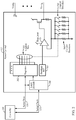
- FIG. 1 schematically illustrates a system 100 comprising a processor 102 and a memory device 104.
- the processor 102 includes a central processing unit (CPU) 106, a controller 108, which may comprise, for example, a finite state machine, a memory interface 110 and a global clock control 112. While the foregoing elements relate to the present disclosure, the processor 102 may constitute a system-on-chip (SOC) and include other conventional elements (not illustrated) necessary for the processor 102 to operate.
- the memory device 104 includes at least one memory die 114, and the memory interface 110 communicates with the memory die 114 via a control bus 116 and a bidirectional data bus 118.
- the memory interface 110 is responsible for managing communication between the processor 102 and the memory device 104.
- the system 100 also includes a power system 120 including a power controller 122 and a plurality of regulators including a first regulator 124, a second regulator 126, a third regulator 128, a fourth regulator 130 and a fifth regulator 132 that together form a reference voltage generator and which, in some embodiments, may comprise an active buffer with a high impedance ladder.
- the processor 102 communicates with the power controller 122 via a serial data bus 131 and a serial clock bus 133.
- the memory interface 110 includes a driver 134 connected to a receiver 136 on the memory die 114 by a first data line 138, and the memory interface 110 includes a receiver 140 connected to a driver 142 on the memory die 114 by a second data line 144.
- the first and second data lines 138, 144 represent logical portions of the bidirectional data bus 118 rather than discrete interconnections and are illustrated separately for ease of description only.
- the memory interface 110 includes on-die termination (ODT) logic 146 that controls a switch 148 for selectively connecting a resistor 150 to the first regulator 124 of the power system 120.
- ODT on-die termination
- the switch 148 is controlled by the ODT logic 146 and by the controller 108 which is connected to the ODT logic 146 by a line 152.
- a resistance is connected to the receiver 140 in the memory interface 110 to terminate the second data line 144 and reduce artifacts that may be produced when signals are transmitted on the second data line 144 of the bidirectional data bus 118 at a high speed.
- the memory die 114 also includes ODT logic 154 that controls a switch 156 for selectively connecting a resistor 158 to the fourth regulator 130 of the power system 120.
- the switch 156 in the memory die 114 is controlled by the ODT logic 154 and by the controller 108 of the processor 102 which is connected to the switch 156 on the memory die 114 by a line 160.
- a resistance is connected to the receiver 136 in the memory die 114 to terminate the first data line 138 and reduce artifacts that may be produced when signals are transmitted on the first data line 138 of the bidirectional data bus 118 at a high speed.
- the system 100 also includes on-board termination (OBT) logic 162 that controls a switch 164 for selectively connecting a resistor 166 to the control bus 116 for selectively connecting the control bus 116 to the fifth regulator 132 of the power system 120.
- ODT on-board termination
- the controller 108 and the OBT logic 162 control the state of the switch 164, and the controller 108 is connected to the OBT logic 162 by a line 168.
- a resistance is connected to the control bus 116 to terminate the control bus 116 and reduce artifacts that may be produced when signals are transmitted on the control bus 116 at a high speed.
- One input of the receiver 140 in the memory interface 110 is connected to the second regulator 126 of the power system 120, and one input of the receiver 136 in the memory die 114 is connected to the third regulator 128 of the power system 120.
- the second regulator 126 and the third regulator 128 provide appropriate reference voltages to the memory interface receiver 140 and the memory die receiver 136 which reference voltages are selected based on the speed that data is being transmitted on the bidirectional data bus 118.
- a "low” data rate is a rate at which data can be efficiently transferred in a system without the use of signal termination and a "high” data rate is a rate at which signal termination is necessary or desirable.
- a medium rate as used herein is a rate high enough that termination of the bidirectional data bus 118 is desirable but low enough that termination of the control bus 116 is not necessary.
- a low data rate might be anything below 400 MHz (800 Mbps), a medium data rate between 400 and 667 MHz, and a high data rate anything above 667 MHz (1333 Mbps).
- these values are programmable and are dependent on the design and sophistication of the printed circuit board routing. Low cost designs with poor impedance and/or trace skew matching may force a lowering of the frequency threshold, and higher quality designs may allow the frequency thresholds to be raised.
- the system 100 is initialized in a conventional manner, and the memory interface 110 communicates with the memory device 104 at a low data rate based in part on the clock speed set by the global clock controller 112. Signal termination is not required when data is transmitted at the low data rate, and the controller 108 maintains the switch 148 in the ODT logic 146 of the memory interface 110 and the switch 156 of the ODT logic 154 of the memory die 114 and the switch 164 of the OBT logic 162 in open states.
- the controller 108 instructs the power system 120 to provide a reference voltage having a first level from the second regulator 126 to the receiver 140 of the memory interface 110 and to provide a second reference voltage, which may be the same as the first reference voltage, to the receiver 136 of the memory die 114.
- the controller 108 may optionally cause the power controller 122 to shut down the first regulator 124, the fourth regulator 130 and the fifth regulator 132 when signal termination is not required in order to achieve additional power savings.
- Various conditions may require a higher data transfer rate between the memory interface 110 and the memory device 104, for example, when the processor 102 begins running a graphics-intensive program. As previously discussed, such a higher data rate requires signal termination for efficient data transfer. This next data rate described herein is referred to herein as a medium rate, and for this rate, signal termination should be provided at both ends of the bidirectional data bus 118. The process of changing the data rate on the bidirectional data bus 118 is described below.
- Data transfer on the bidirectional data bus 118 must be halted or stalled during the transition from one data rate to another. Therefore, when the CPU 106 informs the controller 108 that a shift from the low data rate to a medium data rate is needed, the controller 108 causes the memory interface 110 to complete any outstanding transactions with the memory device 104 and then stop sending data over the bidirectional data bus 118. During this time, the memory device 104 enters in a self-refresh mode to preserve its contents. Next, the controller 108 signals the power controller 122 to cause the second regulator 126 to change the first reference voltage provided to the receiver 140 of the memory interface 110 and to cause the third regulator 128 to change the second reference voltage provided to the receiver 136 of the memory die 114.
- the power supply 120 and the first through fifth regulators 124-132 therein are configured to change voltage quickly and without producing significant noise because the faster the reference voltages can be changed and stabilized, the faster data traffic can resume on the bidirectional data bus 118.
- This voltage change may be accomplished, for example, by using suitable circuitry in the power controller 122 as illustrated in FIG. 2 .
- the controller 108 communicates with the power controller 122 via the serial data bus 131 and the serial clock bus 133. Packets (not illustrated) are transmitted that have a command portion, an address portion and a data portion, and this allows the controller 108 to write, read, and control the power controller 122.
- FIG. 2 illustrates a portion of the power controller 122 that produces an output from the first regulator 124; similar circuitry controls the outputs of the second through fifth regulators 126, 128, 130, 132 but is not specifically illustrated.
- Incoming packets from the controller 108 are inspected by the logic decode 200 which determines what type of operation to perform and where to route the data.
- the packet from the controller 108 writes a binary voltage representation into a corresponding register 202, and the output of the register 202, controls bits 203 to close appropriate ones of control switches 204. This establishes through the control resistors 205 the predetermined Vout for the first regulator 124.
- the first regulator 124 receives an input from a bandgap reference 201 and a second input from the network of control resistors 205 for establishing an output voltage.
- Power controller 122 contains numerous regulators whose voltages can be independently controlled using this scheme. It is also possible for the controller 108 to read information back from the power controller 122, including the control bit 203 values. During a speed switch, numerous voltages in the system 100 may need to be reprogrammed quickly, and this simple and efficient interface permits rapid voltage reprogramming and reduces overall system time.
- the termination voltage that is supplied to the various terminations are directly driven by transistor outputs of the first regulator 124 and corresponding transistor outputs (not illustrated) of the second through fifth regulators 126-132. This results in a very low output impedance and correspondingly faster transient response (compared with a traditional resistor voltage divider) which significantly reduces the duration of the bus stall.
- the termination switches 148, 156, 164 are open, there is no current flow through output transistors of the first through fifth regulators 124-132 (compared with static current flow through a traditional resistor voltage divider).
- the digital re-programmability of all the regulators provides significant flexibility versus traditional resistor voltage divider. For example, DDR3, DDR3L, and DDR4 devices can be supported on identical platforms merely by reprogramming the first through fifth regulators 124-132.
- the controller 108 also signals the ODT logic 146 on the memory interface 110 to close the switch 148 to terminate the second data line 144 and signals the ODT logic 154 on the memory die 114 to close the switch 156 and terminate the first data line 138.
- the power controller 122 must also reactivate the first regulator 124 and the fourth regulator 130 if they were previously powered down for power saving reasons.
- the clock rate is increased from a low rate to a medium rate, and the system 100 will be ready to resume data transfer once the voltages provided by the power system 120 have stabilized. It takes less time to enable the ODT logic 146, 154 on the memory interface 110 and the memory die 114 than to stabilize the voltages provided by the power system 120.
- programmable timers may be used to stall data on the bidirectional data bus 118 for a time long enough to ensure a stable voltage supply. Note that this settling time of the voltages is dependent on platform variables such as the number of memory devices that are sourced by a particular voltage regulator, the number of bypassing capacitors used to quiet that voltage supply, and the construction and sophistication of the printed circuit board (PCB). Therefore, the programmable stall time can be optimized for the system components and PCB construction.
- the controller 108 causes the memory interface 110 to resume communication with the memory die 114, and the memory die 114 ceases its self-refresh operation.
- a status register is updated in the global clock control 112, and, if necessary, an interrupt is sent to the CPU 106.
- the system 100 continues to operate in this manner until a need for yet a higher data transfer speed arises.
- it is also necessary to activate the OBT logic 162 to provide signal termination on the control bus 116.
- Traffic on the bidirectional data bus 118 is stalled as was the case during the transfer from low to medium data rate, and the reference voltages provided by the second regulator 126 and the third regulator 128 to the memory interface 110 and the memory die 114 are adjusted as necessary.
- the controller 108 sends a signal to the OBT logic 162 to cause the OBT logic 162 to close the switch 164 and terminate the signal on the control bus 116.
- this fifth regulator 132 is reactivated at this time as well.
- control data traffic resumes on the control bus 116 and data traffic resumes on the bidirectional data bus 118.
- These same steps are followed in order to reduce the data rate on the bidirectional data bus 118 to the medium or low level, namely, stalling traffic on the respective bus, disabling the ODT and OBT, and changing the reference voltages provided to the receiver 140 on the memory interface 110 and the receiver 136 at the memory die 114.
- system 100 can also transition directly from the low rate condition to the high rate condition by enabling the OBT logic 162 at the same time as the ODT logic 146 of the memory interface 110 and the ODT logic 154 of the memory die 114. These transitions are under the control of the CPU 106 and the controller 108 based on the data transfer rates required by the system 100 and components (not illustrated) connected thereto.
- the system 100 described above beneficially places the control of signal termination at various locations under the control of controller 108 in a manner that allows for the dynamic control of signal termination at multiple locations in the system 100.
- the controller 108 also controls the reference voltages provided to the memory interface 110 and the memory die 114 and stops and starts the transmission of data on the bidirectional data bus 118 and on the control bus 116, the controller 108 can coordinate the stopping of data on the bidirectional data bus 118 and on the control bus 116 with the changes in signal termination and reference voltages in a manner that reduces the time that the bidirectional data bus 118 is unavailable for use by the system 100 and thus obtain energy savings while maintaining acceptable system performance. Additional flexibility is provided by using one platform to handle variations in memory interface standards, bus topology/component population, and PCB construction and routing.
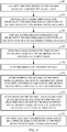
- FIG. 3 illustrates a method according to an embodiment of the disclosure that includes a block 302 of connecting the first device to the second device by a bidirectional data bus, a block 304 of providing first termination logic for selectively terminating signals received at the first device on the bidirectional data bus, and a block 306 of providing second termination logic for selectively terminating signals received at the second device on the bidirectional data bus.
- the method also includes a block 308 of sending first signals from the first device to the second device on the bidirectional data bus at a first speed, a block 310 of stopping the sending of the first signals, and a block 312 of, after stopping the sending of the first signals, enabling the second termination logic and shifting a reference voltage of the second device from a first level to a second level.
- the method includes a block 314 of, after enabling the second termination logic at the second device, sending second signals from the first device to the second device on the bidirectional data bus at a second speed, greater than the first speed, and a block 316 of controlling the first termination logic based on a speed of signals received at the first device on the bidirectional data bus.
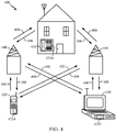
- FIG. 4 illustrates an exemplary wireless communication system 400 in which one or more embodiments of the disclosure may be advantageously employed.
- FIG. 4 shows three remote units 420, 430, and 450 and two base stations 440. It will be recognized that conventional wireless communication systems may have many more remote units and base stations.
- the remote units 420, 430, and 450 include integrated circuit or other semiconductor devices 425A, 425B and 425C (including a system as disclosed herein), which are among embodiments of the disclosure as discussed further below.
- FIG. 4 shows forward link signals 480 from the base stations 440 and the remote units 420, 430, and 450 and reverse link signals 490 from the remote units 420, 430, and 450 to the base stations 440.
- the remote unit 420 is shown as a mobile telephone
- the remote unit 430 is shown as a portable computer
- the remote unit 450 is shown as a fixed location remote unit in a wireless local loop system.
- the remote units may be any one or combination of a mobile phone, hand-held personal communication system (PCS) unit, portable data unit such as a personal data assistant (PDA), navigation device (such as GPS enabled devices), set top box, music player, video player, entertainment unit, fixed location data unit such as meter reading equipment, or any other device that stores or retrieves data or computer instructions, or any combination thereof.
- FIG. 4 illustrates remote units according to the teachings of the disclosure, the disclosure is not limited to these exemplary illustrated units. Embodiments of the disclosure may be suitably employed in any device having active integrated circuitry including memory and on-chip circuitry for test and characterization.
- a software module may reside in RAM memory, flash memory, ROM memory, EPROM memory, EEPROM memory, registers, hard disk, a removable disk, a CD-ROM, or any other form of storage medium known in the art.
- An exemplary storage medium is coupled to the processor such that the processor can read information from, and write information to, the storage medium. In the alternative, the storage medium may be integral to the processor.
- an embodiment of the invention can include a computer readable media embodying a method for causing a controller to selectively control on-die and/or on-board signal termination based on the speed of data on a line being terminated. Accordingly, the invention is not limited to illustrated examples and any means for performing the functionality described herein are included in embodiments of the invention.
Landscapes
- Engineering & Computer Science (AREA)
- Computer Hardware Design (AREA)
- General Engineering & Computer Science (AREA)
- Physics & Mathematics (AREA)
- Theoretical Computer Science (AREA)
- Computing Systems (AREA)
- Mathematical Physics (AREA)
- General Physics & Mathematics (AREA)
- Power Engineering (AREA)
- Computer Networks & Wireless Communication (AREA)
- Signal Processing (AREA)
- Power Sources (AREA)
- Logic Circuits (AREA)
- Dram (AREA)
- Memory System (AREA)
Description
- The present disclosure is directed to a method and apparatus for selectively terminating signals at each end of a bidirectional data bus, and, more specifically, toward a method and apparatus for controlling signal terminations and reference voltages at each end of a bidirectional data bus and for controlling transmission speed on the bidirectional data bus.
- Electronic devices include various pathways on which data must be transferred at high speed. One example of a high-speed data pathway is a data bus between a processor and a memory device. When signaling rates are high, it is generally necessary to use impedance matching signal terminations on pathways to control artifacts such as electrical reflections, inter-symbol interference, overshoot, undershoot, and ringing. Terminations consume significant electrical power, however, and are therefore not used when signal rates are low enough to avoid the foregoing artifacts.
- Devices that use high signal rates and thus require signal termination have heretofore often been AC line powered or contained a sufficiently large battery pack (a laptop, for example) so that the power drain of signal termination circuitry could be ignored. In addition, many electronic components, memory devices such as dynamic random access memory (DRAM) device, for example, contain built-in features like on-die termination (ODT) which selectively terminate signals based on the direction that a signal is travelling. That is, control circuitry on the DRAM device itself selectively enables signal termination during signal reception and disables it at other times.
- Manufacturers continue to look for ways to decrease power use, both to prolong battery life and to reduce the amount of heat that must be dissipated. It would therefore be desirable to provide a system and method for dynamically controlling signal termination that reduces energy use.
US2008/112233A1 relates to semiconductor devices with integrated circuits. - Exemplary embodiments of the invention are described below. A first exemplary embodiment comprises a method of controlling signal termination on at least one bus connecting a first device to a second device. The method includes connecting the first device to the second device by a bidirectional data bus, providing first termination logic for selectively terminating signals received at the first device on the bidirectional data bus, and providing second termination logic for selectively terminating signals received at the second device on the bidirectional data bus. The method also includes sending first signals from the first device to the second device on the bidirectional data bus at a first speed, stopping the sending of the first signals, and, after stopping the sending of the first signals, enabling the second termination logic and shifting a reference voltage of the second device from a first level to a second level. The method further includes, after enabling the second termination logic at the second device, sending second signals from the first device to the second device on the bidirectional data bus at a second speed, greater than the first speed, and controlling the first termination logic based on a speed of signals received at the first device on the bidirectional data bus.
- Another exemplary embodiment includes a system that has a memory interface and a memory device connected to the memory interface by a control bus and by a bidirectional data bus. The system includes first termination logic for selectively terminating signals received at the memory interface on the bidirectional data bus, second termination logic for selectively terminating signals received at the memory device on the bidirectional data bus, and third termination logic for selectively terminating signals received at the memory device on the control bus. The system has a reference voltage generator for providing a first reference voltage to the memory interface and for providing a second reference voltage to the memory device and a controller for selectively enabling the first termination logic and the second termination logic and the third termination logic and for controlling the first and second reference voltages output by the reference voltage generator. The controller also controls data transmission between the memory interface and the memory device on the bidirectional data bus and is configured to selectively enable the first termination logic based on a speed of signals received at the memory interface on the bidirectional data bus and to selectively enable the second termination logic based on a speed of signals received at the memory device on the bidirectional data bus and to selectively enable the third termination logic based on a speed of signals received at the memory device on the control bus. The controller also causes the reference voltage generator to provide a first reference voltage to the memory interface when the first termination logic is enabled and to provide a second reference voltage different than the first reference voltage to the memory interface when the first termination logic is not enabled and to provide a third reference voltage to the memory device when the third termination logic is enabled and to provide a fourth reference voltage different than the third reference voltage to the memory device when the third termination logic is not enabled. The controller is also configured to stop traffic on the bidirectional data bus before enabling or disabling the first termination logic and before enabling or disabling the second termination logic.
- A further exemplary embodiment includes a system having a bidirectional data bus connecting a first device to a second device, first termination means for selectively terminating signals received at the first device on the bidirectional data bus and second termination means for selectively terminating signals received at the second device on the bidirectional data bus. The system also includes means for sending first signals from the first device to the second device on the bidirectional data bus at a first speed and means for stopping the sending of the first signals, and includes means for enabling the second termination means and for shifting a reference voltage of the second device from a first level to a second level after stopping the sending of the first signals. The system also includes means for sending second signals from the first device to the second device on the bidirectional data bus at a second speed, greater than the first speed, after enabling the second termination means at the second device, and means for controlling the first termination means based on a speed of signals received at the first device on the bidirectional data bus.
- Another exemplary embodiment comprises a method of controlling signal termination on at least one bus connecting a first device to a second device that includes steps for connecting the first device to the second device by a bidirectional data bus, steps for providing first termination logic for selectively terminating signals received at the first device on the bidirectional data bus, and steps for providing second termination logic for selectively terminating signals received at the second device on the bidirectional data bus. The method also includes steps for sending first signals from the first device to the second device on the bidirectional data bus at a first speed, steps for stopping the sending of the first signals, and, after stopping the sending of the first signals, steps for enabling the second termination logic and shifting a reference voltage of the second device from a first level to a second level. The method also includes, after enabling the second termination logic at the second device, steps for sending second signals from the first device to the second device on the bidirectional data bus at a second speed, greater than the first speed, and steps for controlling the first termination logic based on a speed of signals received at the first device on the bidirectional data bus.
- Another exemplary embodiment comprises a non-transitory computer readable medium embodying instructions that, when executed by a computer, cause the computer to control signal terminations on at least one bus connecting a first device to a second device by selectively terminating signals received at the first device on the bidirectional data bus, and selectively terminating signals received at the second device on the bidirectional data bus. The instructions are also for causing the first device to send first signals from the first device to the second device on the bidirectional data bus at a first speed, for causing the first device to stop the sending of the first signals, and after causing the first device to stop the sending of the first signals, shifting a reference voltage of the second device from a first level to a second level. The instructions are also for, after enabling the second termination logic at the second device, causing the first device to send signals from the first device to the second device on the bidirectional data bus at a second speed, greater than the first speed, and controlling the first termination logic based on a speed of signals received at the first device on the bidirectional data bus.
- The accompanying drawings are presented to aid in the description of embodiments of the invention and are provided solely for illustration of the embodiments and not limitation thereof.
-
FIG. 1 is a circuit diagram illustrating a system including a processor and a memory device according to an embodiment of the disclosure. -
FIG. 2 is a circuit diagram of a portion of a power controller of the system ofFIG. 1 . -
FIG. 3 is a flow chart illustrating a method according to the disclosure. -
FIG. 4 is a schematic diagram of an exemplary wireless communication system in which embodiments of the disclosure may be used. - Aspects of the invention are disclosed in the following description and related drawings directed to specific embodiments of the invention. Alternate embodiments may be devised without departing from the scope of the invention. Additionally, well-known elements of the invention will not be described in detail or will be omitted so as not to obscure the relevant details of the invention.
- The word "exemplary" is used herein to mean "serving as an example, instance, or illustration." Any embodiment described herein as "exemplary" is not necessarily to be construed as preferred or advantageous over other embodiments. Likewise, the term "embodiments of the invention" does not require that all embodiments of the invention include the discussed feature, advantage or mode of operation.
- The terminology used herein is for the purpose of describing particular embodiments only and is not intended to be limiting of embodiments of the invention. As used herein, the singular forms "a", "an" and "the" are intended to include the plural forms as well, unless the context clearly indicates otherwise. It will be further understood that the terms "comprises", "comprising", "includes", and/or "including", when used herein, specify the presence of stated features, integers, steps, operations, elements, and/or components, but do not preclude the presence or addition of one or more other features, integers, steps, operations, elements, components, and/or groups thereof.
- Further, many embodiments are described in terms of sequences of actions to be performed by, for example, elements of a computing device. It will be recognized that various actions described herein can be performed by specific circuits (e.g., application specific integrated circuits (ASICs)), by program instructions being executed by one or more processors, or by a combination of both. Additionally, these sequence of actions described herein can be considered to be embodied entirely within any form of computer readable storage medium having stored therein a corresponding set of computer instructions that upon execution would cause an associated processor to perform the functionality described herein. Thus, the various aspects of the invention may be embodied in a number of different forms, all of which have been contemplated to be within the scope of the claimed subject matter. In addition, for each of the embodiments described herein, the corresponding form of any such embodiments may be described herein as, for example, "logic configured to" perform the described action.
-
FIG. 1 schematically illustrates asystem 100 comprising aprocessor 102 and amemory device 104. Theprocessor 102 includes a central processing unit (CPU) 106, acontroller 108, which may comprise, for example, a finite state machine, amemory interface 110 and aglobal clock control 112. While the foregoing elements relate to the present disclosure, theprocessor 102 may constitute a system-on-chip (SOC) and include other conventional elements (not illustrated) necessary for theprocessor 102 to operate. Thememory device 104 includes at least one memory die 114, and thememory interface 110 communicates with the memory die 114 via acontrol bus 116 and abidirectional data bus 118. Thememory interface 110 is responsible for managing communication between theprocessor 102 and thememory device 104. Thesystem 100 also includes apower system 120 including apower controller 122 and a plurality of regulators including afirst regulator 124, asecond regulator 126, athird regulator 128, afourth regulator 130 and afifth regulator 132 that together form a reference voltage generator and which, in some embodiments, may comprise an active buffer with a high impedance ladder. Theprocessor 102 communicates with thepower controller 122 via aserial data bus 131 and aserial clock bus 133. - The
memory interface 110 includes adriver 134 connected to areceiver 136 on the memory die 114 by afirst data line 138, and thememory interface 110 includes areceiver 140 connected to a driver 142 on the memory die 114 by asecond data line 144. The first andsecond data lines bidirectional data bus 118 rather than discrete interconnections and are illustrated separately for ease of description only. - The
memory interface 110 includes on-die termination (ODT)logic 146 that controls aswitch 148 for selectively connecting aresistor 150 to thefirst regulator 124 of thepower system 120. Theswitch 148 is controlled by theODT logic 146 and by thecontroller 108 which is connected to theODT logic 146 by aline 152. When theswitch 148 is closed, a resistance is connected to thereceiver 140 in thememory interface 110 to terminate thesecond data line 144 and reduce artifacts that may be produced when signals are transmitted on thesecond data line 144 of thebidirectional data bus 118 at a high speed. The memory die 114 also includes ODT logic 154 that controls a switch 156 for selectively connecting aresistor 158 to thefourth regulator 130 of thepower system 120. The switch 156 in the memory die 114 is controlled by the ODT logic 154 and by thecontroller 108 of theprocessor 102 which is connected to the switch 156 on the memory die 114 by aline 160. When the switch 156 is closed, a resistance is connected to thereceiver 136 in the memory die 114 to terminate thefirst data line 138 and reduce artifacts that may be produced when signals are transmitted on thefirst data line 138 of thebidirectional data bus 118 at a high speed. Thesystem 100 also includes on-board termination (OBT)logic 162 that controls aswitch 164 for selectively connecting aresistor 166 to thecontrol bus 116 for selectively connecting thecontrol bus 116 to thefifth regulator 132 of thepower system 120. Thecontroller 108 and theOBT logic 162 control the state of theswitch 164, and thecontroller 108 is connected to theOBT logic 162 by aline 168. When theswitch 164 is closed, a resistance is connected to thecontrol bus 116 to terminate thecontrol bus 116 and reduce artifacts that may be produced when signals are transmitted on thecontrol bus 116 at a high speed. - One input of the
receiver 140 in thememory interface 110 is connected to thesecond regulator 126 of thepower system 120, and one input of thereceiver 136 in the memory die 114 is connected to thethird regulator 128 of thepower system 120. Thesecond regulator 126 and thethird regulator 128 provide appropriate reference voltages to thememory interface receiver 140 and thememory die receiver 136 which reference voltages are selected based on the speed that data is being transmitted on thebidirectional data bus 118. - The operation of the
system 100 will now be described. Thesystem 100 will be described herein as operating at "low," "medium" and "high" data rates. Without specifically defining these data rates, a "low" data rate is a rate at which data can be efficiently transferred in a system without the use of signal termination and a "high" data rate is a rate at which signal termination is necessary or desirable. A medium rate as used herein is a rate high enough that termination of thebidirectional data bus 118 is desirable but low enough that termination of thecontrol bus 116 is not necessary. In a typical system such as a DDR3 DRAM, a low data rate might be anything below 400 MHz (800 Mbps), a medium data rate between 400 and 667 MHz, and a high data rate anything above 667 MHz (1333 Mbps). However, these values are programmable and are dependent on the design and sophistication of the printed circuit board routing. Low cost designs with poor impedance and/or trace skew matching may force a lowering of the frequency threshold, and higher quality designs may allow the frequency thresholds to be raised. - The
system 100 is initialized in a conventional manner, and thememory interface 110 communicates with thememory device 104 at a low data rate based in part on the clock speed set by theglobal clock controller 112. Signal termination is not required when data is transmitted at the low data rate, and thecontroller 108 maintains theswitch 148 in theODT logic 146 of thememory interface 110 and the switch 156 of the ODT logic 154 of the memory die 114 and theswitch 164 of theOBT logic 162 in open states. In addition, thecontroller 108 instructs thepower system 120 to provide a reference voltage having a first level from thesecond regulator 126 to thereceiver 140 of thememory interface 110 and to provide a second reference voltage, which may be the same as the first reference voltage, to thereceiver 136 of the memory die 114. Because termination is not needed at thememory interface 110 or at the memory die 114 or on thecontrol bus 116, very little power is consumed by theODT logic 146 or the ODT logic 154 or theOBT logic 162; thecontroller 108 may optionally cause thepower controller 122 to shut down thefirst regulator 124, thefourth regulator 130 and thefifth regulator 132 when signal termination is not required in order to achieve additional power savings. - Various conditions may require a higher data transfer rate between the
memory interface 110 and thememory device 104, for example, when theprocessor 102 begins running a graphics-intensive program. As previously discussed, such a higher data rate requires signal termination for efficient data transfer. This next data rate described herein is referred to herein as a medium rate, and for this rate, signal termination should be provided at both ends of thebidirectional data bus 118. The process of changing the data rate on thebidirectional data bus 118 is described below. - Data transfer on the
bidirectional data bus 118 must be halted or stalled during the transition from one data rate to another. Therefore, when theCPU 106 informs thecontroller 108 that a shift from the low data rate to a medium data rate is needed, thecontroller 108 causes thememory interface 110 to complete any outstanding transactions with thememory device 104 and then stop sending data over thebidirectional data bus 118. During this time, thememory device 104 enters in a self-refresh mode to preserve its contents. Next, thecontroller 108 signals thepower controller 122 to cause thesecond regulator 126 to change the first reference voltage provided to thereceiver 140 of thememory interface 110 and to cause thethird regulator 128 to change the second reference voltage provided to thereceiver 136 of the memory die 114. Thepower supply 120 and the first through fifth regulators 124-132 therein are configured to change voltage quickly and without producing significant noise because the faster the reference voltages can be changed and stabilized, the faster data traffic can resume on thebidirectional data bus 118. - This voltage change may be accomplished, for example, by using suitable circuitry in the
power controller 122 as illustrated inFIG. 2 . Thecontroller 108 communicates with thepower controller 122 via theserial data bus 131 and theserial clock bus 133. Packets (not illustrated) are transmitted that have a command portion, an address portion and a data portion, and this allows thecontroller 108 to write, read, and control thepower controller 122. -
FIG. 2 illustrates a portion of thepower controller 122 that produces an output from thefirst regulator 124; similar circuitry controls the outputs of the second throughfifth regulators controller 108 are inspected by thelogic decode 200 which determines what type of operation to perform and where to route the data. To change the voltage Vout from thefirst regulator 124, the packet from thecontroller 108 writes a binary voltage representation into acorresponding register 202, and the output of theregister 202, controlsbits 203 to close appropriate ones of control switches 204. This establishes through thecontrol resistors 205 the predetermined Vout for thefirst regulator 124. Thefirst regulator 124 receives an input from abandgap reference 201 and a second input from the network ofcontrol resistors 205 for establishing an output voltage. -
Power controller 122 contains numerous regulators whose voltages can be independently controlled using this scheme. It is also possible for thecontroller 108 to read information back from thepower controller 122, including thecontrol bit 203 values. During a speed switch, numerous voltages in thesystem 100 may need to be reprogrammed quickly, and this simple and efficient interface permits rapid voltage reprogramming and reduces overall system time. The termination voltage that is supplied to the various terminations are directly driven by transistor outputs of thefirst regulator 124 and corresponding transistor outputs (not illustrated) of the second through fifth regulators 126-132. This results in a very low output impedance and correspondingly faster transient response (compared with a traditional resistor voltage divider) which significantly reduces the duration of the bus stall. In addition, when the termination switches 148, 156, 164 are open, there is no current flow through output transistors of the first through fifth regulators 124-132 (compared with static current flow through a traditional resistor voltage divider). Finally, in a system which may need to support multiple DRAM interface standards, the digital re-programmability of all the regulators provides significant flexibility versus traditional resistor voltage divider. For example, DDR3, DDR3L, and DDR4 devices can be supported on identical platforms merely by reprogramming the first through fifth regulators 124-132. - The
controller 108 also signals theODT logic 146 on thememory interface 110 to close theswitch 148 to terminate thesecond data line 144 and signals the ODT logic 154 on the memory die 114 to close the switch 156 and terminate thefirst data line 138. Thepower controller 122 must also reactivate thefirst regulator 124 and thefourth regulator 130 if they were previously powered down for power saving reasons. The clock rate is increased from a low rate to a medium rate, and thesystem 100 will be ready to resume data transfer once the voltages provided by thepower system 120 have stabilized. It takes less time to enable theODT logic 146, 154 on thememory interface 110 and the memory die 114 than to stabilize the voltages provided by thepower system 120. Therefore, programmable timers (not illustrated) may be used to stall data on thebidirectional data bus 118 for a time long enough to ensure a stable voltage supply. Note that this settling time of the voltages is dependent on platform variables such as the number of memory devices that are sourced by a particular voltage regulator, the number of bypassing capacitors used to quiet that voltage supply, and the construction and sophistication of the printed circuit board (PCB). Therefore, the programmable stall time can be optimized for the system components and PCB construction. When those timers expire, thecontroller 108 causes thememory interface 110 to resume communication with the memory die 114, and the memory die 114 ceases its self-refresh operation. A status register is updated in theglobal clock control 112, and, if necessary, an interrupt is sent to theCPU 106. - The
system 100 continues to operate in this manner until a need for yet a higher data transfer speed arises. In order to switch the data rate on thebidirectional data bus 118 to a high speed, it is also necessary to activate theOBT logic 162 to provide signal termination on thecontrol bus 116. Traffic on thebidirectional data bus 118 is stalled as was the case during the transfer from low to medium data rate, and the reference voltages provided by thesecond regulator 126 and thethird regulator 128 to thememory interface 110 and the memory die 114 are adjusted as necessary. In addition, thecontroller 108 sends a signal to theOBT logic 162 to cause theOBT logic 162 to close theswitch 164 and terminate the signal on thecontrol bus 116. If thefifth regulator 132 is in an inactive state, thisfifth regulator 132 is reactivated at this time as well. Once the voltages provided by thepower supply 120 have stabilized, control data traffic resumes on thecontrol bus 116 and data traffic resumes on thebidirectional data bus 118. These same steps are followed in order to reduce the data rate on thebidirectional data bus 118 to the medium or low level, namely, stalling traffic on the respective bus, disabling the ODT and OBT, and changing the reference voltages provided to thereceiver 140 on thememory interface 110 and thereceiver 136 at the memory die 114. Of course, thesystem 100 can also transition directly from the low rate condition to the high rate condition by enabling theOBT logic 162 at the same time as theODT logic 146 of thememory interface 110 and the ODT logic 154 of the memory die 114. These transitions are under the control of theCPU 106 and thecontroller 108 based on the data transfer rates required by thesystem 100 and components (not illustrated) connected thereto. - The
system 100 described above beneficially places the control of signal termination at various locations under the control ofcontroller 108 in a manner that allows for the dynamic control of signal termination at multiple locations in thesystem 100. In addition, because thecontroller 108 also controls the reference voltages provided to thememory interface 110 and the memory die 114 and stops and starts the transmission of data on thebidirectional data bus 118 and on thecontrol bus 116, thecontroller 108 can coordinate the stopping of data on thebidirectional data bus 118 and on thecontrol bus 116 with the changes in signal termination and reference voltages in a manner that reduces the time that thebidirectional data bus 118 is unavailable for use by thesystem 100 and thus obtain energy savings while maintaining acceptable system performance. Additional flexibility is provided by using one platform to handle variations in memory interface standards, bus topology/component population, and PCB construction and routing. -
FIG. 3 illustrates a method according to an embodiment of the disclosure that includes ablock 302 of connecting the first device to the second device by a bidirectional data bus, ablock 304 of providing first termination logic for selectively terminating signals received at the first device on the bidirectional data bus, and ablock 306 of providing second termination logic for selectively terminating signals received at the second device on the bidirectional data bus. The method also includes ablock 308 of sending first signals from the first device to the second device on the bidirectional data bus at a first speed, ablock 310 of stopping the sending of the first signals, and ablock 312 of, after stopping the sending of the first signals, enabling the second termination logic and shifting a reference voltage of the second device from a first level to a second level. In addition, the method includes ablock 314 of, after enabling the second termination logic at the second device, sending second signals from the first device to the second device on the bidirectional data bus at a second speed, greater than the first speed, and ablock 316 of controlling the first termination logic based on a speed of signals received at the first device on the bidirectional data bus. -
FIG. 4 illustrates an exemplarywireless communication system 400 in which one or more embodiments of the disclosure may be advantageously employed. For purposes of illustration,FIG. 4 shows threeremote units base stations 440. It will be recognized that conventional wireless communication systems may have many more remote units and base stations. Theremote units other semiconductor devices FIG. 4 shows forward link signals 480 from thebase stations 440 and theremote units remote units base stations 440. - In
FIG. 4 , theremote unit 420 is shown as a mobile telephone, theremote unit 430 is shown as a portable computer, and theremote unit 450 is shown as a fixed location remote unit in a wireless local loop system. For example, the remote units may be any one or combination of a mobile phone, hand-held personal communication system (PCS) unit, portable data unit such as a personal data assistant (PDA), navigation device (such as GPS enabled devices), set top box, music player, video player, entertainment unit, fixed location data unit such as meter reading equipment, or any other device that stores or retrieves data or computer instructions, or any combination thereof. AlthoughFIG. 4 illustrates remote units according to the teachings of the disclosure, the disclosure is not limited to these exemplary illustrated units. Embodiments of the disclosure may be suitably employed in any device having active integrated circuitry including memory and on-chip circuitry for test and characterization. - Those of skill in the art will appreciate that information and signals may be represented using any of a variety of different technologies and techniques. For example, data, instructions, commands, information, signals, bits, symbols, and chips that may be referenced throughout the above description may be represented by voltages, currents, electromagnetic waves, magnetic fields or particles, optical fields or particles, or any combination thereof.
- Further, those of skill in the art will appreciate that the various illustrative logical blocks, modules, circuits, and algorithm steps described in connection with the embodiments disclosed herein may be implemented as electronic hardware, computer software, or combinations of both. To clearly illustrate this interchangeability of hardware and software, various illustrative components, blocks, modules, circuits, and steps have been described above generally in terms of their functionality. Whether such functionality is implemented as hardware or software depends upon the particular application and design constraints imposed on the overall system. Skilled artisans may implement the described functionality in varying ways for each particular application, but such implementation decisions should not be interpreted as causing a departure from the scope of the present invention.
- The methods, sequences and/or algorithms described in connection with the embodiments disclosed herein may be embodied directly in hardware, in a software module executed by a processor, or in a combination of the two. A software module may reside in RAM memory, flash memory, ROM memory, EPROM memory, EEPROM memory, registers, hard disk, a removable disk, a CD-ROM, or any other form of storage medium known in the art. An exemplary storage medium is coupled to the processor such that the processor can read information from, and write information to, the storage medium. In the alternative, the storage medium may be integral to the processor.
- Accordingly, an embodiment of the invention can include a computer readable media embodying a method for causing a controller to selectively control on-die and/or on-board signal termination based on the speed of data on a line being terminated. Accordingly, the invention is not limited to illustrated examples and any means for performing the functionality described herein are included in embodiments of the invention.
- While the foregoing disclosure shows illustrative embodiments of the invention, it should be noted that various changes and modifications could be made herein without departing from the scope of the invention as defined by the appended claims. The functions, steps and/or actions of the method claims in accordance with the embodiments of the invention described herein need not be performed in any particular order. Furthermore, although elements of the invention may be described or claimed in the singular, the plural is contemplated unless limitation to the singular is explicitly stated.
Claims (15)
- A method of controlling signal termination on at least one bus connecting a first device to a second device, the method characterized by:connecting (302) the first device to the second device by a bidirectional data bus;providing (304) a first termination logic for selectively terminating signals received at the first device on the bidirectional data bus;providing (306) a second termination logic for selectively terminating signals received at the second device on the bidirectional data bus;sending (308) first signals from the first device to the second device on the bidirectional data bus at a first speed;stopping (310) the sending of the first signals;after stopping the sending of the first signals, enabling (312) the second termination logic and shifting a reference voltage of the second device from a first level to a second level;after enabling the second termination logic at the second device, sending (314) second signals from the first device to the second device on the bidirectional data bus at a second speed, greater than the first speed; andcontrolling (316) the first termination logic based on a speed of signals received at the first device on the bidirectional data bus.
- The method of claim 1, wherein the first device includes a memory controller and the second device is a memory device.
- The method of claim 2, further comprising connecting the first device to the second device by a control bus.
- The method of claim 3, further comprising providing a third termination logic for selectively terminating signals received at the memory device on the control bus.
- The method of claim 4, wherein the first termination logic comprises a first on-die termination (ODT) logic on the memory controller, the second termination logic comprises a second ODT logic at the memory device and the third termination logic comprise an on-board termination (OBT) logic.
- The method of claim 4, further comprising providing a controller and controlling the first termination logic and the second termination logic and the third termination logic using the controller.
- The method of claim 4, wherein the first termination logic comprises a first ODT logic on the memory controller, the second termination logic comprises a second ODT logic at the memory device and the third termination logic comprise an OBT logic, and
wherein the first ODT logic includes a resistor and a switch for connecting the resistor to a voltage source, the method including disabling the voltage source when the signals received at the first device on the bidirectional data bus are not terminated. - The method of claim 1 further comprising:stopping the sending of the second signals;after stopping the sending of the second signals, disabling the second termination logic at the second device and shifting the reference voltage of the second device from the second level to the first level; andafter disabling the termination logic at the second device, sending the first signals from the first device to the second device at the first speed.
- The method of claim 1, further comprising providing a controller and controlling the first termination logic and the second termination logic using the controller, wherein controlling the first termination logic comprises writing a binary voltage representation into a register.
- The method of claim 1, wherein the first termination logic includes a resistor and a switch for connecting the resistor to a voltage source, the method including disabling the voltage source when the signals received at the first device on the bidirectional data bus are not terminated.
- The method of claim 1 wherein enabling the second termination logic comprises sending a first control signal from the first device to the second device.
- The method of claim 1, wherein the first device comprises a memory controller and the second device is a dynamic random access memory (DRAM) device.
- The method of claim 1,
wherein the first device comprises a memory controller and the second device is a memory device,
wherein the first termination logic comprises a first ODT logic on a memory interface, and the second termination logic comprises a second ODT logic at the memory device, and
wherein enabling the second termination logic comprises sending a first control signal from the memory interface to the second ODT logic. - A system (100) characterized by:a bidirectional data bus (118) connecting a first device (110) to a second device (114);first termination means (146) for selectively terminating signals received at the first device (110) on the bidirectional data bus (118);second termination means (156) for selectively terminating signals received at the second device (114) on the bidirectional data bus (118);means (138) for sending first signals from the first device (110) to the second device (114) on the bidirectional data bus (118) at a first speed;means (108) for stopping the sending of the first signals;means (108) for enabling the second termination means and shifting a reference voltage of the second device from a first level to a second level after stopping the sending of the first signals;means (144) for sending second signals from the first device to the second device on the bidirectional data bus at a second speed, greater than the first speed, after enabling the second termination means at the second device; andmeans (108) for controlling the first termination means based on a speed of signals received at the first device on the bidirectional data bus.
- The system of claim 14, further comprising providing third termination means for selectively terminating signals received at the second device on a control bus.
Priority Applications (3)
| Application Number | Priority Date | Filing Date | Title |
|---|---|---|---|
| RS20170544A RS56030B1 (en) | 2013-03-07 | 2014-03-06 | PROCEDURE AND DEVICE FOR SELECTIVE SIGNALING OF THE SIGNAL ON THE BIDIRECTIONAL ROAD ON THE BASIS OF THE ROAD SPEED |
| HRP20170912TT HRP20170912T1 (en) | 2013-03-07 | 2014-03-06 | PROCEDURE AND APPARATUS FOR SELECTIVE SIGNAL TERMINATION ON THE BIDIRECTIONAL ROAD ON THE BASIS OF THE ROAD SPEED |
| SM20170382T SMT201700382T1 (en) | 2013-03-07 | 2014-03-06 | Method and apparatus for selectively terminating signals on a bidirectional bus based on bus speed |
Applications Claiming Priority (2)
| Application Number | Priority Date | Filing Date | Title |
|---|---|---|---|
| US13/787,926 US9088445B2 (en) | 2013-03-07 | 2013-03-07 | Method and apparatus for selectively terminating signals on a bidirectional bus based on bus speed |
| PCT/US2014/021401 WO2014138477A1 (en) | 2013-03-07 | 2014-03-06 | Method and apparatus for selectively terminating signals on a bidirectional bus based on bus speed |
Publications (2)
| Publication Number | Publication Date |
|---|---|
| EP2965217A1 EP2965217A1 (en) | 2016-01-13 |
| EP2965217B1 true EP2965217B1 (en) | 2017-04-19 |
Family
ID=50442620
Family Applications (1)
| Application Number | Title | Priority Date | Filing Date |
|---|---|---|---|
| EP14716075.8A Active EP2965217B1 (en) | 2013-03-07 | 2014-03-06 | Method and apparatus for selectively terminating signals on a bidirectional bus based on bus speed |
Country Status (9)
| Country | Link |
|---|---|
| US (2) | US9088445B2 (en) |
| EP (1) | EP2965217B1 (en) |
| JP (1) | JP6158960B2 (en) |
| KR (1) | KR101742763B1 (en) |
| CN (1) | CN105190584B (en) |
| HR (1) | HRP20170912T1 (en) |
| RS (1) | RS56030B1 (en) |
| SM (1) | SMT201700382T1 (en) |
| WO (1) | WO2014138477A1 (en) |
Families Citing this family (7)
| Publication number | Priority date | Publication date | Assignee | Title |
|---|---|---|---|---|
| US9088445B2 (en) * | 2013-03-07 | 2015-07-21 | Qualcomm Incorporated | Method and apparatus for selectively terminating signals on a bidirectional bus based on bus speed |
| US9542305B2 (en) * | 2015-01-16 | 2017-01-10 | Harman International Industries, Inc. | Impedance matching for high speed signaling in memory system |
| TWI705666B (en) * | 2015-06-15 | 2020-09-21 | 日商新力股份有限公司 | Transmission device, receiving device, communication system |
| US9910482B2 (en) * | 2015-09-24 | 2018-03-06 | Qualcomm Incorporated | Memory interface with adjustable voltage and termination and methods of use |
| KR102529187B1 (en) * | 2016-03-31 | 2023-05-04 | 삼성전자주식회사 | Reception interface circuit supporting multiple communication standards and memory system including the same |
| US9825730B1 (en) * | 2016-09-26 | 2017-11-21 | Dell Products, Lp | System and method for optimizing link performance with lanes operating at different speeds |
| JP7383831B2 (en) | 2020-09-23 | 2023-11-20 | キオクシア株式会社 | Semiconductor storage devices and memory systems |
Family Cites Families (20)
| Publication number | Priority date | Publication date | Assignee | Title |
|---|---|---|---|---|
| US5467455A (en) | 1993-11-03 | 1995-11-14 | Motorola, Inc. | Data processing system and method for performing dynamic bus termination |
| JPH1020974A (en) * | 1996-07-03 | 1998-01-23 | Fujitsu Ltd | Bus structure and input / output buffer |
| US6557066B1 (en) * | 1999-05-25 | 2003-04-29 | Lsi Logic Corporation | Method and apparatus for data dependent, dual level output driver |
| JP3651410B2 (en) * | 2001-05-14 | 2005-05-25 | セイコーエプソン株式会社 | Transmission circuit, data transfer control device, and electronic device |
| JP3756818B2 (en) * | 2002-01-09 | 2006-03-15 | 株式会社メガチップス | Memory control circuit and control system |
| US6894691B2 (en) | 2002-05-01 | 2005-05-17 | Dell Products L.P. | Dynamic switching of parallel termination for power management with DDR memory |
| AU2005227500B2 (en) * | 2004-03-24 | 2008-12-04 | Qualcomm Incorporated | High data rate interface apparatus and method |
| US7173450B2 (en) | 2004-06-01 | 2007-02-06 | Hewlett-Packard Development Company, L.P. | Bus controller |
| KR100670702B1 (en) | 2004-10-30 | 2007-01-17 | 주식회사 하이닉스반도체 | Semiconductor memory device with on-die termination circuit |
| KR100801033B1 (en) * | 2005-11-03 | 2008-02-04 | 삼성전자주식회사 | Semiconductor device capable of testing on die termination circuit using boundary scan circuit, test system having same, and test method |
| JP4615461B2 (en) * | 2006-03-10 | 2011-01-19 | 京セラミタ株式会社 | Memory controller |
| KR100790821B1 (en) | 2006-11-15 | 2008-01-03 | 삼성전자주식회사 | On-die termination circuit in semiconductor memory device |
| US7864183B1 (en) | 2007-03-08 | 2011-01-04 | Nvidia Corporation | Dynamic switching of memory termination characteristics in a graphics system |
| US7746098B2 (en) | 2008-03-10 | 2010-06-29 | Qimonda North America Corp. | Termination switching based on data rate |
| KR101039862B1 (en) * | 2008-11-11 | 2011-06-13 | 주식회사 하이닉스반도체 | A semiconductor memory device having a clocking mode and a method of operating the same |
| KR100980417B1 (en) * | 2008-12-09 | 2010-09-07 | 주식회사 하이닉스반도체 | Data driver |
| KR100980425B1 (en) | 2008-12-30 | 2010-09-07 | 주식회사 하이닉스반도체 | Global I / O Line Termination Control Circuit |
| KR101789077B1 (en) * | 2010-02-23 | 2017-11-20 | 삼성전자주식회사 | On-die termination circuit, data output buffer, semiconductor memory device, memory module, method of operating an on-die termination circuit, method of operating a data output buffer and method of training on-die termination |
| US8274308B2 (en) | 2010-06-28 | 2012-09-25 | Intel Corporation | Method and apparatus for dynamic memory termination |
| US9088445B2 (en) * | 2013-03-07 | 2015-07-21 | Qualcomm Incorporated | Method and apparatus for selectively terminating signals on a bidirectional bus based on bus speed |
-
2013
- 2013-03-07 US US13/787,926 patent/US9088445B2/en active Active
-
2014
- 2014-03-06 JP JP2015561679A patent/JP6158960B2/en not_active Expired - Fee Related
- 2014-03-06 SM SM20170382T patent/SMT201700382T1/en unknown
- 2014-03-06 RS RS20170544A patent/RS56030B1/en unknown
- 2014-03-06 HR HRP20170912TT patent/HRP20170912T1/en unknown
- 2014-03-06 KR KR1020157027341A patent/KR101742763B1/en not_active Expired - Fee Related
- 2014-03-06 EP EP14716075.8A patent/EP2965217B1/en active Active
- 2014-03-06 WO PCT/US2014/021401 patent/WO2014138477A1/en not_active Ceased
- 2014-03-06 CN CN201480012111.2A patent/CN105190584B/en active Active
-
2015
- 2015-03-19 US US14/663,303 patent/US9246716B2/en active Active
Non-Patent Citations (1)
| Title |
|---|
| None * |
Also Published As
| Publication number | Publication date |
|---|---|
| US20140253173A1 (en) | 2014-09-11 |
| KR101742763B1 (en) | 2017-06-01 |
| JP2016514316A (en) | 2016-05-19 |
| CN105190584A (en) | 2015-12-23 |
| EP2965217A1 (en) | 2016-01-13 |
| SMT201700382T1 (en) | 2017-09-07 |
| CN105190584B (en) | 2018-10-30 |
| JP6158960B2 (en) | 2017-07-05 |
| US20150194959A1 (en) | 2015-07-09 |
| RS56030B1 (en) | 2017-09-29 |
| WO2014138477A1 (en) | 2014-09-12 |
| KR20150126895A (en) | 2015-11-13 |
| US9246716B2 (en) | 2016-01-26 |
| HRP20170912T1 (en) | 2017-09-22 |
| US9088445B2 (en) | 2015-07-21 |
Similar Documents
| Publication | Publication Date | Title |
|---|---|---|
| US9246716B2 (en) | Method and apparatus for selectively terminating signals on a bidirectional bus based on bus speed | |
| EP2406896B1 (en) | Data interface power consumption control | |
| EP1430673B1 (en) | Apparatus and method for power efficient line driver | |
| US10541019B2 (en) | Apparatuses and methods for dynamic voltage and frequency switching for dynamic random access memory | |
| US7689852B2 (en) | Method and system for providing power management for an integrated gigabit ethernet controller | |
| US10162402B2 (en) | Serial communication method | |
| US20170280385A1 (en) | Link speed control systems for power optimization | |
| US20150370305A1 (en) | Systems and methods for providing power savings and interference mitigation on physical transmission media | |
| KR20180020983A (en) | Low power physical layer driver topologies | |
| WO2010020837A1 (en) | Voltage regulator with low and high power modes | |
| CN114397955B (en) | Memory interface with adjustable voltage and termination and method of use | |
| KR101205324B1 (en) | Methods for controlling power of system with serial interface manner | |
| CN102253910A (en) | A kind of I2C transmission method and its device | |
| US10014846B2 (en) | Increasing output amplitude of a voltage-mode driver in a low supply voltage technology | |
| EP2992400B1 (en) | Frequency power manager | |
| JP6950187B2 (en) | Circuit equipment, electronic devices and cable harnesses | |
| US10833899B2 (en) | Low power physical layer driver topologies | |
| US8339162B2 (en) | Circuit device and method of controlling circuit device | |
| CN121002491A (en) | Chip select transmitter for multiple signal levels | |
| HK40022896B (en) | Power down mode for universal flash storage (ufs) |
Legal Events
| Date | Code | Title | Description |
|---|---|---|---|
| PUAI | Public reference made under article 153(3) epc to a published international application that has entered the european phase |
Free format text: ORIGINAL CODE: 0009012 |
|
| 17P | Request for examination filed |
Effective date: 20150730 |
|
| AK | Designated contracting states |
Kind code of ref document: A1 Designated state(s): AL AT BE BG CH CY CZ DE DK EE ES FI FR GB GR HR HU IE IS IT LI LT LU LV MC MK MT NL NO PL PT RO RS SE SI SK SM TR |
|
| AX | Request for extension of the european patent |
Extension state: BA ME |
|
| DAX | Request for extension of the european patent (deleted) | ||
| REG | Reference to a national code |
Ref country code: DE Ref legal event code: R079 Ref document number: 602014008809 Country of ref document: DE Free format text: PREVIOUS MAIN CLASS: G06F0013400000 Ipc: H03K0019017500 |
|
| GRAP | Despatch of communication of intention to grant a patent |
Free format text: ORIGINAL CODE: EPIDOSNIGR1 |
|
| RIC1 | Information provided on ipc code assigned before grant |
Ipc: H04L 25/02 20060101ALI20161005BHEP Ipc: H03K 19/0175 20060101AFI20161005BHEP |
|
| INTG | Intention to grant announced |
Effective date: 20161026 |
|
| STAA | Information on the status of an ep patent application or granted ep patent |
Free format text: STATUS: GRANT OF PATENT IS INTENDED |
|
| GRAS | Grant fee paid |
Free format text: ORIGINAL CODE: EPIDOSNIGR3 |
|
| GRAA | (expected) grant |
Free format text: ORIGINAL CODE: 0009210 |
|
| STAA | Information on the status of an ep patent application or granted ep patent |
Free format text: STATUS: THE PATENT HAS BEEN GRANTED |
|
| AK | Designated contracting states |
Kind code of ref document: B1 Designated state(s): AL AT BE BG CH CY CZ DE DK EE ES FI FR GB GR HR HU IE IS IT LI LT LU LV MC MK MT NL NO PL PT RO RS SE SI SK SM TR |
|
| REG | Reference to a national code |
Ref country code: GB Ref legal event code: FG4D |
|
| REG | Reference to a national code |
Ref country code: CH Ref legal event code: EP |
|
| REG | Reference to a national code |
Ref country code: AT Ref legal event code: REF Ref document number: 886821 Country of ref document: AT Kind code of ref document: T Effective date: 20170515 |
|
| REG | Reference to a national code |
Ref country code: IE Ref legal event code: FG4D |
|
| REG | Reference to a national code |
Ref country code: DE Ref legal event code: R096 Ref document number: 602014008809 Country of ref document: DE |
|
| REG | Reference to a national code |
Ref country code: HR Ref legal event code: TUEP Ref document number: P20170912 Country of ref document: HR |
|
| REG | Reference to a national code |
Ref country code: EE Ref legal event code: FG4A Ref document number: E013825 Country of ref document: EE Effective date: 20170517 |
|
| REG | Reference to a national code |
Ref country code: NL Ref legal event code: MP Effective date: 20170419 |
|
| REG | Reference to a national code |
Ref country code: LT Ref legal event code: MG4D |
|
| REG | Reference to a national code |
Ref country code: AT Ref legal event code: MK05 Ref document number: 886821 Country of ref document: AT Kind code of ref document: T Effective date: 20170419 |
|
| REG | Reference to a national code |
Ref country code: HR Ref legal event code: T1PR Ref document number: P20170912 Country of ref document: HR |
|
| PG25 | Lapsed in a contracting state [announced via postgrant information from national office to epo] |
Ref country code: NL Free format text: LAPSE BECAUSE OF FAILURE TO SUBMIT A TRANSLATION OF THE DESCRIPTION OR TO PAY THE FEE WITHIN THE PRESCRIBED TIME-LIMIT Effective date: 20170419 |
|
| PG25 | Lapsed in a contracting state [announced via postgrant information from national office to epo] |
Ref country code: LT Free format text: LAPSE BECAUSE OF FAILURE TO SUBMIT A TRANSLATION OF THE DESCRIPTION OR TO PAY THE FEE WITHIN THE PRESCRIBED TIME-LIMIT Effective date: 20170419 Ref country code: FI Free format text: LAPSE BECAUSE OF FAILURE TO SUBMIT A TRANSLATION OF THE DESCRIPTION OR TO PAY THE FEE WITHIN THE PRESCRIBED TIME-LIMIT Effective date: 20170419 Ref country code: NO Free format text: LAPSE BECAUSE OF FAILURE TO SUBMIT A TRANSLATION OF THE DESCRIPTION OR TO PAY THE FEE WITHIN THE PRESCRIBED TIME-LIMIT Effective date: 20170719 Ref country code: ES Free format text: LAPSE BECAUSE OF FAILURE TO SUBMIT A TRANSLATION OF THE DESCRIPTION OR TO PAY THE FEE WITHIN THE PRESCRIBED TIME-LIMIT Effective date: 20170419 Ref country code: GR Free format text: LAPSE BECAUSE OF FAILURE TO SUBMIT A TRANSLATION OF THE DESCRIPTION OR TO PAY THE FEE WITHIN THE PRESCRIBED TIME-LIMIT Effective date: 20170720 Ref country code: AT Free format text: LAPSE BECAUSE OF FAILURE TO SUBMIT A TRANSLATION OF THE DESCRIPTION OR TO PAY THE FEE WITHIN THE PRESCRIBED TIME-LIMIT Effective date: 20170419 |
|
| PG25 | Lapsed in a contracting state [announced via postgrant information from national office to epo] |
Ref country code: PL Free format text: LAPSE BECAUSE OF FAILURE TO SUBMIT A TRANSLATION OF THE DESCRIPTION OR TO PAY THE FEE WITHIN THE PRESCRIBED TIME-LIMIT Effective date: 20170419 Ref country code: BG Free format text: LAPSE BECAUSE OF FAILURE TO SUBMIT A TRANSLATION OF THE DESCRIPTION OR TO PAY THE FEE WITHIN THE PRESCRIBED TIME-LIMIT Effective date: 20170719 Ref country code: SE Free format text: LAPSE BECAUSE OF FAILURE TO SUBMIT A TRANSLATION OF THE DESCRIPTION OR TO PAY THE FEE WITHIN THE PRESCRIBED TIME-LIMIT Effective date: 20170419 Ref country code: LV Free format text: LAPSE BECAUSE OF FAILURE TO SUBMIT A TRANSLATION OF THE DESCRIPTION OR TO PAY THE FEE WITHIN THE PRESCRIBED TIME-LIMIT Effective date: 20170419 |
|
| REG | Reference to a national code |
Ref country code: SK Ref legal event code: T3 Ref document number: E 24831 Country of ref document: SK |
|
| REG | Reference to a national code |
Ref country code: DE Ref legal event code: R097 Ref document number: 602014008809 Country of ref document: DE |
|
| PG25 | Lapsed in a contracting state [announced via postgrant information from national office to epo] |
Ref country code: CZ Free format text: LAPSE BECAUSE OF FAILURE TO SUBMIT A TRANSLATION OF THE DESCRIPTION OR TO PAY THE FEE WITHIN THE PRESCRIBED TIME-LIMIT Effective date: 20170419 Ref country code: DK Free format text: LAPSE BECAUSE OF FAILURE TO SUBMIT A TRANSLATION OF THE DESCRIPTION OR TO PAY THE FEE WITHIN THE PRESCRIBED TIME-LIMIT Effective date: 20170419 Ref country code: RO Free format text: LAPSE BECAUSE OF FAILURE TO SUBMIT A TRANSLATION OF THE DESCRIPTION OR TO PAY THE FEE WITHIN THE PRESCRIBED TIME-LIMIT Effective date: 20170419 |
|
| PLBE | No opposition filed within time limit |
Free format text: ORIGINAL CODE: 0009261 |
|
| REG | Reference to a national code |
Ref country code: FR Ref legal event code: PLFP Year of fee payment: 5 |
|
| STAA | Information on the status of an ep patent application or granted ep patent |
Free format text: STATUS: NO OPPOSITION FILED WITHIN TIME LIMIT |
|
| 26N | No opposition filed |
Effective date: 20180122 |
|
| PGFP | Annual fee paid to national office [announced via postgrant information from national office to epo] |
Ref country code: GB Payment date: 20180223 Year of fee payment: 5 |
|
| PG25 | Lapsed in a contracting state [announced via postgrant information from national office to epo] |
Ref country code: SI Free format text: LAPSE BECAUSE OF FAILURE TO SUBMIT A TRANSLATION OF THE DESCRIPTION OR TO PAY THE FEE WITHIN THE PRESCRIBED TIME-LIMIT Effective date: 20170419 |
|
| PGFP | Annual fee paid to national office [announced via postgrant information from national office to epo] |
Ref country code: IT Payment date: 20180315 Year of fee payment: 5 Ref country code: FR Payment date: 20180223 Year of fee payment: 5 |
|
| REG | Reference to a national code |
Ref country code: CH Ref legal event code: PL |
|
| PG25 | Lapsed in a contracting state [announced via postgrant information from national office to epo] |
Ref country code: MC Free format text: LAPSE BECAUSE OF FAILURE TO SUBMIT A TRANSLATION OF THE DESCRIPTION OR TO PAY THE FEE WITHIN THE PRESCRIBED TIME-LIMIT Effective date: 20170419 |
|
| REG | Reference to a national code |
Ref country code: BE Ref legal event code: MM Effective date: 20180331 |
|
| REG | Reference to a national code |
Ref country code: IE Ref legal event code: MM4A |
|
| PG25 | Lapsed in a contracting state [announced via postgrant information from national office to epo] |
Ref country code: LU Free format text: LAPSE BECAUSE OF NON-PAYMENT OF DUE FEES Effective date: 20180306 |
|
| PG25 | Lapsed in a contracting state [announced via postgrant information from national office to epo] |
Ref country code: IE Free format text: LAPSE BECAUSE OF NON-PAYMENT OF DUE FEES Effective date: 20180306 |
|
| PG25 | Lapsed in a contracting state [announced via postgrant information from national office to epo] |
Ref country code: CH Free format text: LAPSE BECAUSE OF NON-PAYMENT OF DUE FEES Effective date: 20180331 Ref country code: LI Free format text: LAPSE BECAUSE OF NON-PAYMENT OF DUE FEES Effective date: 20180331 Ref country code: BE Free format text: LAPSE BECAUSE OF NON-PAYMENT OF DUE FEES Effective date: 20180331 |
|
| REG | Reference to a national code |
Ref country code: HR Ref legal event code: ODRP Ref document number: P20170912 Country of ref document: HR Payment date: 20190227 Year of fee payment: 6 |
|
| GBPC | Gb: european patent ceased through non-payment of renewal fee |
Effective date: 20190306 |
|
| PG25 | Lapsed in a contracting state [announced via postgrant information from national office to epo] |
Ref country code: GB Free format text: LAPSE BECAUSE OF NON-PAYMENT OF DUE FEES Effective date: 20190306 |
|
| PG25 | Lapsed in a contracting state [announced via postgrant information from national office to epo] |
Ref country code: IT Free format text: LAPSE BECAUSE OF NON-PAYMENT OF DUE FEES Effective date: 20190306 Ref country code: FR Free format text: LAPSE BECAUSE OF NON-PAYMENT OF DUE FEES Effective date: 20190331 |
|
| REG | Reference to a national code |
Ref country code: HR Ref legal event code: ODRP Ref document number: P20170912 Country of ref document: HR Payment date: 20200303 Year of fee payment: 7 |
|
| PG25 | Lapsed in a contracting state [announced via postgrant information from national office to epo] |
Ref country code: TR Free format text: LAPSE BECAUSE OF FAILURE TO SUBMIT A TRANSLATION OF THE DESCRIPTION OR TO PAY THE FEE WITHIN THE PRESCRIBED TIME-LIMIT Effective date: 20170419 |
|
| PG25 | Lapsed in a contracting state [announced via postgrant information from national office to epo] |
Ref country code: PT Free format text: LAPSE BECAUSE OF FAILURE TO SUBMIT A TRANSLATION OF THE DESCRIPTION OR TO PAY THE FEE WITHIN THE PRESCRIBED TIME-LIMIT Effective date: 20170419 |
|
| PG25 | Lapsed in a contracting state [announced via postgrant information from national office to epo] |
Ref country code: CY Free format text: LAPSE BECAUSE OF FAILURE TO SUBMIT A TRANSLATION OF THE DESCRIPTION OR TO PAY THE FEE WITHIN THE PRESCRIBED TIME-LIMIT Effective date: 20170419 Ref country code: HU Free format text: LAPSE BECAUSE OF FAILURE TO SUBMIT A TRANSLATION OF THE DESCRIPTION OR TO PAY THE FEE WITHIN THE PRESCRIBED TIME-LIMIT; INVALID AB INITIO Effective date: 20140306 |
|
| REG | Reference to a national code |
Ref country code: DE Ref legal event code: R082 Ref document number: 602014008809 Country of ref document: DE Representative=s name: MAUCHER JENKINS PATENTANWAELTE & RECHTSANWAELT, DE |
|
| REG | Reference to a national code |
Ref country code: HR Ref legal event code: ODRP Ref document number: P20170912 Country of ref document: HR Payment date: 20210218 Year of fee payment: 8 |
|
| REG | Reference to a national code |
Ref country code: HR Ref legal event code: ODRP Ref document number: P20170912 Country of ref document: HR Payment date: 20220303 Year of fee payment: 9 |
|
| REG | Reference to a national code |
Ref country code: HR Ref legal event code: ODRP Ref document number: P20170912 Country of ref document: HR Payment date: 20221230 Year of fee payment: 10 |
|
| REG | Reference to a national code |
Ref country code: HR Ref legal event code: ODRP Ref document number: P20170912 Country of ref document: HR Payment date: 20240219 Year of fee payment: 11 |
|
| REG | Reference to a national code |
Ref country code: HR Ref legal event code: ODRP Ref document number: P20170912 Country of ref document: HR Payment date: 20250213 Year of fee payment: 12 |
|
| PGFP | Annual fee paid to national office [announced via postgrant information from national office to epo] |
Ref country code: SM Payment date: 20251222 Year of fee payment: 13 |
|
| PGFP | Annual fee paid to national office [announced via postgrant information from national office to epo] |
Ref country code: MT Payment date: 20251220 Year of fee payment: 13 |
|
| REG | Reference to a national code |
Ref country code: HR Ref legal event code: ODRP Ref document number: P20170912 Country of ref document: HR Payment date: 20260219 Year of fee payment: 13 |
|
| PGFP | Annual fee paid to national office [announced via postgrant information from national office to epo] |
Ref country code: DE Payment date: 20260213 Year of fee payment: 13 |
|
| PGFP | Annual fee paid to national office [announced via postgrant information from national office to epo] |
Ref country code: HR Payment date: 20260219 Year of fee payment: 13 |
|
| PGFP | Annual fee paid to national office [announced via postgrant information from national office to epo] |
Ref country code: RS Payment date: 20260113 Year of fee payment: 13 |
|
| PGFP | Annual fee paid to national office [announced via postgrant information from national office to epo] |
Ref country code: IS Payment date: 20260305 Year of fee payment: 13 |
|
| PGFP | Annual fee paid to national office [announced via postgrant information from national office to epo] |
Ref country code: EE Payment date: 20260217 Year of fee payment: 13 Ref country code: SK Payment date: 20260209 Year of fee payment: 13 |
|
| PGFP | Annual fee paid to national office [announced via postgrant information from national office to epo] |
Ref country code: MK Payment date: 20260217 Year of fee payment: 13 |
|
| PGFP | Annual fee paid to national office [announced via postgrant information from national office to epo] |
Ref country code: AL Payment date: 20260306 Year of fee payment: 13 |