EP2961068A1 - Driving device and driving method - Google Patents
Driving device and driving method Download PDFInfo
- Publication number
- EP2961068A1 EP2961068A1 EP15173768.1A EP15173768A EP2961068A1 EP 2961068 A1 EP2961068 A1 EP 2961068A1 EP 15173768 A EP15173768 A EP 15173768A EP 2961068 A1 EP2961068 A1 EP 2961068A1
- Authority
- EP
- European Patent Office
- Prior art keywords
- signal
- control signal
- driving
- unit
- input terminal
- Prior art date
- Legal status (The legal status is an assumption and is not a legal conclusion. Google has not performed a legal analysis and makes no representation as to the accuracy of the status listed.)
- Granted
Links
Images









Classifications
-
- H—ELECTRICITY
- H02—GENERATION; CONVERSION OR DISTRIBUTION OF ELECTRIC POWER
- H02H—EMERGENCY PROTECTIVE CIRCUIT ARRANGEMENTS
- H02H3/00—Emergency protective circuit arrangements for automatic disconnection directly responsive to an undesired change from normal electric working condition with or without subsequent reconnection ; integrated protection
- H02H3/02—Details
- H02H3/05—Details with means for increasing reliability, e.g. redundancy arrangements
-
- H—ELECTRICITY
- H02—GENERATION; CONVERSION OR DISTRIBUTION OF ELECTRIC POWER
- H02M—APPARATUS FOR CONVERSION BETWEEN AC AND AC, BETWEEN AC AND DC, OR BETWEEN DC AND DC, AND FOR USE WITH MAINS OR SIMILAR POWER SUPPLY SYSTEMS; CONVERSION OF DC OR AC INPUT POWER INTO SURGE OUTPUT POWER; CONTROL OR REGULATION THEREOF
- H02M1/00—Details of apparatus for conversion
- H02M1/08—Circuits specially adapted for the generation of control voltages for semiconductor devices incorporated in static converters
- H02M1/088—Circuits specially adapted for the generation of control voltages for semiconductor devices incorporated in static converters for the simultaneous control of series or parallel connected semiconductor devices
-
- H—ELECTRICITY
- H02—GENERATION; CONVERSION OR DISTRIBUTION OF ELECTRIC POWER
- H02M—APPARATUS FOR CONVERSION BETWEEN AC AND AC, BETWEEN AC AND DC, OR BETWEEN DC AND DC, AND FOR USE WITH MAINS OR SIMILAR POWER SUPPLY SYSTEMS; CONVERSION OF DC OR AC INPUT POWER INTO SURGE OUTPUT POWER; CONTROL OR REGULATION THEREOF
- H02M1/00—Details of apparatus for conversion
- H02M1/32—Means for protecting converters other than automatic disconnection
-
- H—ELECTRICITY
- H03—ELECTRONIC CIRCUITRY
- H03K—PULSE TECHNIQUE
- H03K17/00—Electronic switching or gating, i.e. not by contact-making and –breaking
- H03K17/08—Modifications for protecting switching circuit against overcurrent or overvoltage
- H03K17/082—Modifications for protecting switching circuit against overcurrent or overvoltage by feedback from the output to the control circuit
- H03K17/0822—Modifications for protecting switching circuit against overcurrent or overvoltage by feedback from the output to the control circuit in field-effect transistor switches
-
- H—ELECTRICITY
- H03—ELECTRONIC CIRCUITRY
- H03K—PULSE TECHNIQUE
- H03K17/00—Electronic switching or gating, i.e. not by contact-making and –breaking
- H03K17/10—Modifications for increasing the maximum permissible switched voltage
- H03K17/102—Modifications for increasing the maximum permissible switched voltage in field-effect transistor switches
-
- H—ELECTRICITY
- H03—ELECTRONIC CIRCUITRY
- H03K—PULSE TECHNIQUE
- H03K17/00—Electronic switching or gating, i.e. not by contact-making and –breaking
- H03K17/51—Electronic switching or gating, i.e. not by contact-making and –breaking characterised by the components used
- H03K17/56—Electronic switching or gating, i.e. not by contact-making and –breaking characterised by the components used by the use, as active elements, of semiconductor devices
- H03K17/687—Electronic switching or gating, i.e. not by contact-making and –breaking characterised by the components used by the use, as active elements, of semiconductor devices the devices being field-effect transistors
- H03K17/689—Electronic switching or gating, i.e. not by contact-making and –breaking characterised by the components used by the use, as active elements, of semiconductor devices the devices being field-effect transistors with galvanic isolation between the control circuit and the output circuit
- H03K17/691—Electronic switching or gating, i.e. not by contact-making and –breaking characterised by the components used by the use, as active elements, of semiconductor devices the devices being field-effect transistors with galvanic isolation between the control circuit and the output circuit using transformer coupling
-
- H—ELECTRICITY
- H03—ELECTRONIC CIRCUITRY
- H03K—PULSE TECHNIQUE
- H03K3/00—Circuits for generating electric pulses; Monostable, bistable or multistable circuits
- H03K3/02—Generators characterised by the type of circuit or by the means used for producing pulses
- H03K3/021—Generators characterised by the type of circuit or by the means used for producing pulses by the use, as active elements, of more than one type of element or means, e.g. BIMOS, composite devices such as IGBT
Definitions
- the present invention relates to an electronic device and a method for controlling the same. More particularly, the present invention relates to a driving device and a driving method.
- the way of transmitting the driving signal plays a critical role. If an error occurs in the transmission process of the driving signal, the driving device cannot effectively control the serially-connected IGBTs.
- the driving device may use a logic level signal with a high-to-low voltage level, e.g. the pulse-width-modulation (PWM) signal, as a control signal for driving the serially-connected IGBTs.
- PWM pulse-width-modulation
- the transmission process of the PWM signal modulates the PWM signal into a positive-negative pulse signal, which is transmitted using a transformer, and then the positive-negative pulse signal is demodulated by a demodulating circuit to obtain the driving signal. Subsequently, the above-mentioned driving signal is used to drive the serially-connected IGBTs.
- the driving device is in an abnormal status generates severe electromagnetic interruption; in this case, the last negative pulse signal of the modulated PWM signal will be interfered and hence cannot be successfully demodulated by the demodulating circuit. As such, the serially-connected IGBT that should have been turned off will not be turned off.
- One aspect of the present disclosure is directed to a driving device, which is configured to drive the power semiconductor switch module based on a main control signal.
- Said driving device comprises a voltage-modulating unit and a driving module.
- the voltage-modulating unit receives the protection signal
- the voltage-modulating unit generates a turn-off pulse signal based on the protection signal.
- said driving module is configured to turn off the power semiconductor switch module based on the turn-off pulse signal.
- Said driving method drives a power semiconductor switch module based on a main control signal.
- Said driving method comprises the following steps: when receiving a protection signal, generating a turn-off pulse signal based on the protection signal; and turning off the power semiconductor switch module based on the turn-off pulse signal.
- embodiments of the present disclosure provide a driving device and a driving method to improve the problems of failure to drive the power semiconductor switch module correctly caused by the driving signal being interrupted during the transmission process.
- Couple refers to the direct or indirect physical or electrical contact between or among two or more components, or the mutual operation or action of two or more components.
- the present disclosure provides a driving device; the driving mechanism of said driving device can normally drive the switch component despite the occurrence of the interruption. Said driving device and driving mechanism thereof are described in detail hereinbelow.
- FIG 1A is a schematic diagram of a driving device 100 according to one embodiment of the present disclosure.
- the driving device 100 drives the power semiconductor switch module 900 based on the main control signal PWM (a logic level signal with a high-to-low voltage level).
- the driving device 100 comprises a voltage-modulating unit 110, a transforming unit 120 and a driving module 130.
- the voltage-modulating unit 110 is coupled with the transforming unit 120
- the transforming unit 120 is coupled with the driving module 130.
- the voltage-modulating unit 110 receives the protection signal S pro , the voltage-modulating unit 110 generates a turn-off pulse signal based on the protection signal S pro . Subsequently, the transforming unit 120 transmits the turn-off pulse signal from the voltage-modulating unit 110 to the driving module 130.
- the driving module 130 turns off the power semiconductor switch module 900 based on the turn-off pulse signal.
- said turn-off pulse signal can be a negative pulse signal.
- Said negative pulse signal is not limited to the types of current or voltage.
- the pulse-width of said negative pulse signal is wider than the pulse-width of the negative-narrow pulse signal that is commonly used to turn off the power semiconductor switch module. Subsequently, the driving module 130 turns off the power semiconductor switch module 900 based on the wider negative pulse signal.
- the voltage-modulating unit 110 of the driving device 100 receives the protection signal S pro , the voltage-modulating unit 110 generates a turn-off pulse signal, and since the pulse-width of the turn-off pulse signal is wider, it can make sure that the driving module 130 can effectively turn off the power semiconductor switch module 900 based on the turn-off pulse signal.
- the main control signal PWM would be modulated into the positive-narrow pulse signal and the negative-narrow pulse signal by the voltage-modulating unit 110, wherein the positive-narrow pulse signal is a turn-on pulse signal (for example, the width of the turn-on pulse signal can be any value of 50 ns-10 ⁇ s) configured to turn on the power semiconductor power module 900; the negative-narrow pulse signal is a turn-off pulse signal (for example, the width of the turn-off pulse signal can be any value of 50 ns-10 ⁇ s) configured to turn off the power semiconductor switch module 900, and the positive-narrow pulse signal and the negative-narrow pulse signal are transmitted to the driving module 130 via the transforming unit 120.
- the positive-narrow pulse signal is a turn-on pulse signal (for example, the width of the turn-on pulse signal can be any value of 50 ns-10 ⁇ s) configured to turn on the power semiconductor power module 900
- the negative-narrow pulse signal is a turn-off pulse signal (for example, the width of
- the driving module 130 demodulates and amplifies the positive-narrow pulse signal and the negative-narrow pulse signal to generate the driving signal for turning-on and turning-off the power semiconductor switch module 900.
- the driving module 130 receives the positive-narrow pulse signal
- the received positive-narrow pulse signal is latched at a high voltage level
- the driving module 130 receives the negative-narrow pulse signal the received negative-narrow pulse signal is latched at a low voltage level.
- the driving module 130 restores the received positive-narrow pulse signal and negative-narrow pulse signal into the driving signal having the high-to-low voltage level, and amplifies the driving signal, thereby allowing it to drive the power semiconductor switch module 900.
- the driving module 130 may comprise a driving unit 132 and a driving unit 134
- the power semiconductor switch module 900 may comprise a power semiconductor switch 910 and a power semiconductor switch 920.
- the driving unit 132 is coupled with the power semiconductor switch 910
- the driving unit 134 is coupled with the power semiconductor switch 920.
- the driving unit 132 is configured to drive the power semiconductor switch 910
- the driving unit 134 is configured to drive the power semiconductor switch 920.
- the present disclosure is not limited to the circuit arrangement shown in Figure 1A , persons having ordinary skill in the art may flexibly arrange the number of the power semiconductor switch in the power semiconductor switch module 900 and arrange the number of the driving unit in the driving module 130 correspondingly depending on the actual needs, so as to allow the driving module 130 may effectively drive the power semiconductor switch module 900.
- the power semiconductor switch 910 and the power semiconductor switch 920 can be serially-connected, said two serially-connected power semiconductor switches 910, 920 can be a part of an upper-bridge arm/lower-bridge arm, or they can be the whole upper-bridge arm/lower-bridge arm.
- the power semiconductor switch module 900 may only comprise a single power semiconductor switch, and correspondingly, the driving module 130 may only comprise a single driving unit, depending on the actual needs.
- FIG 1B is a schematic diagram of a transforming unit 120 of a driving device 100 according to another embodiment of the present disclosure.
- the transforming unit 120 illustrated in Figure 1A can be implemented by the structure shown in Figure 1B .
- the transformer of said transforming unit 120 comprises a primary winding and at least one secondary winding.
- the transformer comprises a primary winding 1 and the secondary winding(s) 1_1 ⁇ 1_j 1 , where j 1 is a positive integer, and so on.
- the primary winding 1 of said transformer is coupled with the voltage-modulating unit 110, while the secondary winding 1_1 ⁇ 1_j 1 of the transformer is coupled with the driving unit 132, 134 of the driving module 130.
- the transforming unit 120 may also comprise a plurality of transformers, the structure of these transformer is the same as the structure shown in Figure 1B , and hence will not be described herein in detail; the primary windings of these transformer are serially-connected, and the two terminals of the structure composed of the serially-connected primary windings are electrically coupled with the voltage-modulating unit 110.
- FIG. 1C is a schematic diagram of a transforming unit 120 of a driving device 100 according to yet another embodiment of the present disclosure.
- the transforming unit 120 illustrated in Figure 1A can be implemented by the structure shown in Figure 1C .
- the transforming unit 120 may comprise N transformers; each transformer comprises a primary winding and a secondary winding.
- the primary windings of all the transformers are serially-connected, and the two terminals of the structure composed of the serially-connected primary windings are electrically coupled with the voltage-modulating unit 110.
- each secondary winding of each transformer is electrically coupled with the driving unit 132, 134 of the driving module 130.
- the present disclosure is not limited to the circuit arrangement shown in Figure 1B and Figure 1C , which is only provided to exemplify one embodiment of the present disclosure.
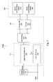
- FIG. 2 is a schematic diagram of a driving device 100A according to another embodiment of the present disclosure. Compared with Figure 1A , Figure 2 illustrates an implementation of the voltage-modulating unit 110. As illustrated in Figure 2 , the voltage-modulating unit 110 comprises a signal processing unit 112 and a turn-off circuit 114. Regarding the structural connection, the signal processing unit 112 is coupled between the turn-off circuit 114 and the transforming unit 120. In operation, the signal processing unit 112 receives the main control signal PWM. Moreover, the turn-off circuit 114 receives the protection signal S pro and generates a driving-regulating signal VT based on the protection signal S pro .
- the signal processing unit 112 generates a turn-off pulse signal based on the driving-regulating signal VT.
- Said turn-off pulse signal is transmitted to the driving module 130 via the transforming unit 120 to turn off the power semiconductor switch module 900.
- the present disclosure is not limited to the circuit arrangement shown in Figure 2 , which is only provided to exemplify one embodiment of the present disclosure.
- FIG 3 is a schematic diagram of a driving device 100B according to embodiments of the present disclosure.
- the driving device 100B of Figure 3 further comprises a control circuit 150.
- the control circuit 150 is coupled with the signal processing unit 112. In operation, initially, the control circuit 150 is used to provide the main control signal PWM to the signal processing unit 112. However, once the control circuit 150 receives the protection signal S pro , the control circuit 150 stops providing the main control signal PWM to the signal processing unit 112.
- the present disclosure is not limited to the circuit arrangement shown in Figure 3 , which is only provided to exemplify one embodiment of the present disclosure.
- the power semiconductor switch module 900 shown in Figure 3 is only one power semiconductor switch module of the inverter.
- the inverter may comprise a plurality of power semiconductor switch modules (not shown), and these power semiconductor switch module can be serially-connected, and each power semiconductor switch module may comprise one or more power semiconductor switches, these power semiconductor switches can be connected in series or in parallel, and the control circuit 150, after receiving the protection signal S pro , can turn off all the power semiconductor switch modules in the whole inverter, so that the whole system stops operating.
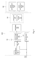
- FIG 4 is a schematic diagram of a driving device 100C according to embodiments of the present disclosure. Compared with Figure 3 , Figure 4 illustrates one implementation of the signal processing unit 112.
- the signal processing unit 112 comprises a logic unit 111 and a pulse-width modulating unit 113.
- the control circuit 150 is coupled with the logic unit 111
- the logic unit 111 is coupled with the pulse-width modulating unit 113
- the pulse-width modulating unit 113 is coupled between the turn-off circuit 114 and the transforming unit 120.
- the pulse-width modulating unit 113 receives the driving-regulating signal and generates a turn-off pulse signal based on the driving-regulating signal VT.
- Said turn-off pulse signal is transmitted to the driving module 130 via the transforming unit 120 to turn off the power semiconductor switch module 900.
- the logic unit 111 is used to receive the main control signal PWM and provide the main control signal PWM to the pulse-width modulating unit 113. However, once the logic circuit 111 receives the protection signal S pro , the logic unit 111 performs logic operation to the main control signal PWM and protection signal S pro so as to stop providing the main control signal PWM to the pulse-width modulating unit 113.
- the logic unit 111 can be implemented using the NOR scheme.
- the logic unit 111 After the logic unit 111 receives the protection signal S pro , the logic unit 111 firstly performs logic operation to the protection signal S pro and the main control signal PWM, so as to stop providing the main control signal PWM. In other words, the logic unit 111 outputs a low level signal.
- control circuit 150 and the logic unit 111 may receive the protection signal S pro at the same time. Subsequently, the logic unit 111 stops providing the main control signal PWM to the pulse-width modulating unit 113, while the control circuit 150, after receiving the protection signal S pro , stops providing the main control signal PWM to the logic unit 111, so as to turn off all the power semiconductor switch modules of the whole inverter, so that the whole system stops operating.
- the present disclosure is not limited to the circuit arrangement shown in Figure 4 , which is only provided to exemplify one embodiment of the present disclosure.
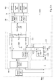
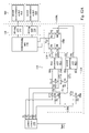
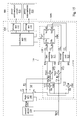
- Figure 5A is a schematic diagram of a driving device 100D according to embodiments of the present disclosure.
- Figure 5A illustrates an implementation of a logic unit 111.
- the logic unit 111 receives the main control signal PWM, so as to output the first control signal P1 and the second control signal P2.
- the output time of the first control signal P1 and the output time of the second control signal P2 are spaced by a pre-determined delay time. Said pre-determined time can be determined depending on actual conditions.
- the logic unit 111 receives the protection signal S pro
- the logic unit 111 performs logic operation to the main control signal PWM and the protection signal S pro , so as to stop outputting the first control signal P1 and the second control signal P2.
- the logic unit 111 may comprise a logic gate circuit 111A and a delay circuit 111B.
- the logic gate circuit 111A is coupled between the control circuit 150 and the delay circuit 111 B.
- the logic gate circuit 111A receives the main control signal PWM to output the first control signal P1.
- the delay circuit 111 B is configured to receive and perform delay operation to the first control signal P1 to generate a second control signal P2. Therefore, the output time of the first control signal P1 and the output time of the second control signal P2 are spaced by a pre-determined delay time.
- Figure 5A illustrates one implementation of the pulse-width modulating unit 113 and the turn-off circuit 114.
- the pulse-width modulating unit 113 comprises a first input terminal IN1 and a second input terminal IN2.
- the first input terminal IN1 of the pulse-width modulating unit 113 is coupled with the logic gate circuit 111A, while the second input terminal IN2 is coupled with the delay circuit 111 B.
- the turn-off circuit 114 is configured to receive the protection signal and generate a first driving-regulating signal VT1 and a second driving-regulating signal VT2 based on the protection signal S pro .
- the first input terminal IN1 can receive the first control signal P1 and the first driving-regulating signal VT1, while the second input terminal IN2 can receive the second control signal P2 and the second driving-regulating signal VT2.
- the turn-off circuit 114 receives the protection signal S pro
- the pulse-width modulating unit 113 generates a turn-off pulse signal based on the first driving-regulating signal VT1 and the second driving-regulating signal VT2.
- the turn-off circuit 114 comprises an input terminal 114A, a level-lowering unit 114B and a level-elevating unit 114C.
- the level-lowering unit 114B is coupled between the input terminal 114A and the first input terminal IN1 of the pulse-width modulating unit 113
- the level-elevating unit 114C is coupled between the input terminal 114A and the second input terminal IN2 of the pulse-width modulating unit 113.
- the level-lowering unit 114B In operation, when the level-lowering unit 114B receives the protection signal S pro , the level-lowering unit 114B outputs the first driving-regulating signal VT1 to the first input terminal IN1 of the pulse-width modulating unit 113, thereby lowering the first input terminal IN1 to a low level.
- the level-elevating unit 114C receives the protection signal S pro , the level-elevating unit 114C outputs the second driving-regulating signal VT2 to the second input terminal IN2 of the pulse-width modulating unit 113, thereby elevating the second input terminal IN2 to the high level.
- the pulse-width modulating unit 113 generates a turn-off pulse signal based on the first driving-regulating signal VT1 and the second driving-regulating signal VT2; that is, the pulse-width modulating unit 113 generates a turn-off pulse signal based on the low level of the first input terminal IN1 and the high level of the second input terminal IN2.
- Said turn-off pulse signal is transmitted to the driving module 130 via the transforming unit 120 to turn off the power semiconductor switch module 900.
- the level-lowering unit 114B comprises a transistor Q2.
- Said transistor Q2 comprises a first terminal, a control terminal and a second terminal.
- the first terminal is coupled with the first input terminal IN1 of the pulse-width modulating unit 113
- the control terminal is coupled with the input terminal 114A of the turn-off circuit 114
- the second terminal is coupled with the ground terminal 800.
- the level-elevating unit 114C comprises a transistor Q1.
- Said transistor Q1 comprises a first terminal, a control terminal, and a second terminal.
- the first terminal is coupled with the second input terminal IN2 of the pulse-width modulating unit 113, and the control terminal is coupled with the input terminal 114A of the turn-off circuit 114.
- the second terminal can be configured to receive the power supply V cc .
- the turn-off circuit 114 further comprises a pulse-width modulator 114D.
- Said pulse-width modulator 114D is coupled between the input terminal 114A of the turn-off circuit 114 and the control terminal of the transistor Q1, and is configured to adjust the pulse-width of turn-off pulse signal.
- the pulse-width modulator 114D comprises a capacitor C1 and a resistor R1, and the capacitor C1 and resistor R1 respectively comprise a first terminal and a second terminal.
- the first terminal of the capacitor C1 is coupled with the input terminal 114A of the turn-off circuit 114, the first terminal of the resistor R1 is coupled with the second terminal of the capacitor C1, while the second terminal of the resistor R1 is coupled with the control terminal of the transistor Q1.
- the present disclosure is not limited to the circuit arrangement shown in Figure 5A , which is only provided to exemplify one embodiment of the present disclosure.
- Figure 5B is a schematic diagram of the waveform of the driving device 100D according to embodiments of the present disclosure.
- the schematic waveform of the driving device 100D is measured when the protection signal S pro arrives after the main control signal PWM wave (during the turn-off process).
- waveforms Sa ⁇ Se respectively corresponds to the waveforms measured at points A ⁇ E marked in Figure 5A .
- the waveform Sa of the main control signal PWM is at low level, indicating that at time point t1, the main control signal PWM has completed.
- the protection signal S pro is generated.
- the voltage-modulating unit 110 generates a positive-narrow pulse signal, a negative-narrow pulse signal and a turn-off pulse signal based on the main control signal PWM and the protection signal S pro , which are transmitted to the driving module 130 via the transforming unit 120, and demodulated and amplified by the driving module 130, so as to generate a driving signal for turning on and turning off the power semiconductor switches 910, 920 of the power semiconductor switch module 900.
- Figure 5C is a schematic diagram of the waveform of the driving device 100D according to embodiments of the present disclosure.
- the schematic waveform of the driving device 100D is measured when the protection signal S pro arrives during the main control signal PWM wave (during the turn-on process).
- waveforms Sa ⁇ Se respectively corresponds to the waveforms measured at points A ⁇ E marked in Figure 5A .
- the waveforms Sa of the main control signal PWM is at the high level, indicating that it's during the turn-on process.
- the protection signal S pro is generated.
- the voltage-modulating unit 110 generates a positive-narrow pulse signal and a turn-off pulse signal based on the main control signal PWM and the protection signal S pro , which is transferred to the driving module 130 via the transforming unit 120, and demodulated and amplified by the driving module 130 so as to generate a driving signal for turning on and turning off the power semiconductor switch modules 910, 920 of the power semiconductor switch module 900.
- FIG. 6 is a schematic diagram of a driving device 100 100E according to embodiments of the present disclosure.
- the signal processing unit 112 of the Figure 6 may not require the logic unit 111.
- the operation method of the control circuit 150 is slightly different.
- Said control circuit 150 outputs the first control signal P1 and the second control signal P2.
- the main control signal comprises the first control signal P1, the second control signal P2.
- the output time of the first control signal P1 and the output time of the second control signal P2 are spaced by a pre-determined delay time, said pre-determined delay time may be determined depending on actual needs.
- control circuit 150 outputs the first control signal P1
- the signal processing unit 112 further comprises a delay circuit configured to receive and perform delay operation to the first control signal P1 so as to generate a second control signal P2; therefore, the output time of the first control signal P1 and the output time of the second control signal P2 are spaced by said pre-determined delay time.
- FIG. 7 is a schematic diagram of a driving device100F according to another embodiment of the present disclosure.
- the signal processing unit 112 of the driving device 100F of Figure 7 further comprises a logic unit 111, said logic unit 111 is coupled with the control circuit 150 and a pulse-width modulating unit 113, and is configured to receive and provide the first control signal P1 and the second control signal P2.
- the logic unit 111 receives the protection signal S pro
- the logic unit 111 performs logic operation to the first and the second control signals P1, P2 and protection signal S pro , so as to stop outputting the first control signal P1 and the second control signal P2.
- the name of the electronic component in Figure 7 is the same as that in Figure 6 , it means that the two electronic components have the common electrical operation means, and hence, detailed description thereof is omitted herein for the sake of brevity.
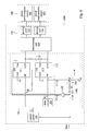
- FIG 8 is a schematic diagram of a driving device 100G according to yet another embodiment of the present disclosure.
- the control circuit 150 can be configured to output the first control signal P1
- the voltage-modulating unit 110 comprises a delay circuit 115
- the delay circuit 115 can be configured to receive and perform delay operation to the first control signal P1, so as to generate a second control signal P2.
- the pulse-width modulating unit 113 comprises a first processing unit IC1 and a second processing unit IC2.
- first processing unit IC1 and the second processing unit IC2 respectively comprise an input terminal IN and an enabling terminal EN.
- the input terminal IN of the first processing unit IC1 is coupled with the control circuit 150
- the enabling terminal EN of the first processing unit IC1 is coupled with the turn-off circuit 114
- the input terminal IN of the second processing unit IC2 is coupled with the delay circuit 115 and the turn-off circuit 114.
- the input terminal IN of the first processing unit IC1 may be configured to receive the first control signal P1, while the enabling terminal EN of the first processing unit IC1 is configured to receive the first driving-regulating signal VT1.
- the input terminal IN of the second processing unit IC2 may be configured to receive the second control signal P2 and the second driving-regulating signal VT2, while the enabling terminal EN of the second processing unit IC2 is configured to receive the voltage V DD .
- the turn-off circuit 114 When the turn-off circuit 114 receives the protection signal S pro , the turn-off circuit 114 generates a first driving-regulating signal VT1, and the enabling terminal EN of the first processing unit IC1 makes the first processing unit IC1 be in a disabled operation mode based on the first driving-regulating signal VT1; meanwhile, the second processing unit IC2 is in an enabled operation mode, and therefore, the output terminal OUT of the first processing unit IC1 and the output terminal OUT of the second processing unit IC2 generate a turn-off pulse signal based on the first driving-regulating signal VT1 and the second driving-regulating signal VT2.
- the turn-off circuit 114 comprises a phase inverter 114E.
- the phase inverter 114E is coupled between the enabling terminal EN of the first processing unit IC1 and the input terminal 114A of the turn-off circuit 114.
- the phase inverter 114E is configured to invert the phase of the protection signal S pro so as to generate a first driving-regulating signal VT1 to the enabling terminal EN of the first processing unit IC1.
- the turn-off circuit 114A comprises a level-elevating unit 114C.
- the level-elevating unit 114C is coupled between input terminal 114A of the turn-off circuit and the input terminal IN of the second processing unit IC2. In operation, when the level-elevating unit 114C receives the protection signal S pro , the level-elevating unit 114C outputs the second driving-regulating signal VT2.
- the level-elevating unit 114C comprises a transistor Q1.
- Said transistor Q1 comprises a first terminal, a control terminal, and a second terminal.
- the first terminal is coupled with the input terminal IN of the second processing unit IC2
- the control terminal is coupled with the input terminal 114A of the turn-off circuit 114.
- the second terminal may be configured to receive the power supply V cc .
- the turn-off circuit 114 further comprises a pulse-width modulator 114D.
- the pulse-width modulator 114D is coupled between the input terminal 114A of the turn-off circuit 114 and the control terminal of the transistor Q1, and is configured to adjust the pulse-width of turn-off pulse signal. More specifically, the pulse-width modulator 114D comprises a capacitor C1 and a resistor R1, while the capacitor C1 and the resistor R1 respectively comprise a first terminal and a second terminal. Regarding the structural connection, the first terminal of the capacitor C1 is coupled with the input terminal 114A of the turn-off circuit 114, the first terminal of the resistor R1 is coupled with the second terminal of the capacitor C1, while the second terminal of the resistor R1 is coupled with the control terminal of the transistor Q1.
- the present disclosure is not limited to the circuit arrangement shown in Figure 8 , which is only provided to exemplify one embodiment of the present disclosure.
- FIG. 9 is a schematic diagram of a driving device 100H according to embodiments of the present disclosure.
- the driving device 100H illustrated in Figure 9 may not require a delay circuit 115.
- the operation method of the control circuit 150 is slightly different.
- Said control circuit 150 outputs the first control signal P1 and the second control signal P2.
- the output time of the first control signal P1 and the output time of the second control signal P2 are spaced by a pre-determined delay time, said pre-determined delay time may be determined depending on actual needs.
- the name of the electronic component in Figure 9 is the same as that in Figure 8 , it means that the two electronic components have the common electrical operation means, and hence, detailed description thereof is omitted herein for the sake of brevity.
- FIG 10 is a schematic diagram of a driving device 100I according to embodiments of the present disclosure.
- a level-lowering unit 114B is used to substitute the phase inverter 114E of the turn-off circuit 114 shown in Figure 8 .
- Said level-lowering unit 114B is coupled between the input terminal 114A and the first processing unit IC1, and is configured to receive a voltage.
- the level-lowering unit 114B receives the protection signal S pro
- the level-lowering unit 114B disables the enabling terminal EN of the first processing unit IC1 so as to generate a first driving-regulating signal VT1, that is, the first processing unit IC1 is in a disabled mode.
- the level-lowering unit 114B comprises a transistor Q2.
- Said transistor Q2 comprises a first terminal, a control terminal and a second terminal.
- the first terminal is coupled with the enabling terminal EN of the first processing unit IC1
- the control terminal is coupled with the input terminal 114A of the turn-off circuit 114
- the second terminal is coupled with ground terminal 800.
- the present disclosure is not limited to the circuit arrangement shown in Figure 10 , which is only provided to exemplify one embodiment of the present disclosure.
- FIG 11 is a schematic diagram of a driving device 100J according to embodiments of the present disclosure.
- the driving device 100J shown in Figure 11 may not require a delay circuit 115.
- the operation method of the control circuit 150 is slightly different.
- Said control circuit 150 outputs the first control signal P1 and the second control signal P2.
- the output time of the first control signal P1 and the output time of the second control signal P2 are spaced by a pre-determined delay time, said pre-determined delay time may be determined depending on actual needs.
- the name of the electronic component in Figure 11 is the same as that in Figure 10 , it means that the two electronic components have the common electrical operation means, and hence, detailed description thereof is omitted herein for the sake of brevity.
- FIG 12A is a schematic diagram of a driving device 100K according to embodiments of the present disclosure.
- the driving device 100K comprises a voltage-modulating unit 110, a transforming unit 120, and a driving module 130.
- the voltage-modulating unit 110 is coupled with the transforming unit 120
- the transforming unit 120 is coupled with the driving module 130.
- the voltage-modulating unit 110 comprises a turn-off circuit 114, a first processing module IC1, a second processing module IC2 and a full-bridge circuit 118.
- the first processing module IC1 comprises a first input terminal IN1 and a second input terminal IN2;
- the second processing module IC2 comprises a first input terminal IN1 and a second input terminal IN2.
- the first processing module IC1 and the second processing module IC2 are respectively coupled with the turn-off circuit 114, while the full-bridge circuit 118 is coupled between the first processing module IC1 and the second processing module IC2.
- the turn-off circuit 114 is configured to receive the protection signal and generates a first driving-regulating signal VT1, a second driving-regulating signal VT2, a third driving-regulating signal VT3 and a fourth driving-regulating signal VT4 based on the protection signal S pro .
- the first input terminal IN1 of the first processing module IC1 is configured to receive he first control signal P1 and first driving-regulating signal VT1, and generate a first output signal O1 based on the first control signal P1 and first driving-regulating signal VT1.
- the second input terminal IN2 of the first processing module IC1 is configured to receive the second control signal P2 and the second driving-regulating signal VT2, and generate a second output signal 02 based on the second control signal P2 and the second driving-regulating signal VT2.
- the first input terminal IN1 of the second processing module IC2 is configured to receive on the third control signal P3 and third driving-regulating signal VT3, and generate a third output signal 03 based on the third control signal P3 and third driving-regulating signal VT3.
- the second input terminal IN2 of the second processing module IC2 is configured to receive the fourth control signal P4 and fourth driving-regulating signal VT4, and generate a fourth output signal 04 based on the fourth control signal P4 and the fourth driving-regulating signal VT4.
- the main control signal comprises the first control signal P1, the second control signal P2, the third control signal P3 and the fourth control signal P4.
- the turn-off circuit 114 receives the protection signal S pro
- the full-bridge circuit 118 is configured to generate a turn-off pulse signal based on the first output signal O1, the second output signal 02, the third output signal 03 and the fourth output signal 04.
- the turn-off circuit 114 comprises an input terminal 114A, a first level-lowering unit and a second level-lowering unit. More specifically, the first level-lowering unit comprises a transistor Qa and a resistor Ra, the second level-lowering unit comprises a transistor Qd and a resistor Rd; the transistor Qa and transistor Qd respectively comprise a first terminal, a control terminal and a second terminal. Regarding the structural connection, the first terminal of the transistor Qa is coupled with the first input terminal IN1 of the first processing module IC1, the control terminal of the transistor Qa is coupled with the input terminal 114A of the turn-off circuit 114 via the resistor Ra, the second terminal is configured to be coupled with a ground terminal Gnd.
- the first terminal of the transistor Qa is coupled with the first input terminal IN1 of the first processing module IC1
- the control terminal of the transistor Qa is coupled with the input terminal 114A of the turn-off circuit 114 via the resistor Ra
- the second terminal is configured to be coupled with a ground terminal Gnd.
- the first terminal of the transistor Qd is coupled with the second input terminal IN2 of the second processing module IC2
- the control terminal of the transistor Qd is coupled with the input terminal 114A of the turn-off circuit 114 via the resistor Rd
- the second terminal of the transistor Qd is configured to be coupled with the ground terminal Gnd.
- the first level-lowering unit when the first level-lowering unit receives the protection signal S pro , the first level-lowering unit outputs a first driving-regulating signal VT1 to the first input terminal IN1 of the first processing module IC1.
- the second level-lowering unit receives the protection signal S pro , the second level-lowering unit outputs a fourth driving-regulating signal VT4 to the second input terminal IN2 of the second processing module IC2.
- the turn-off circuit 114 comprises a first level-elevating unit and a second level-elevating unit. More specifically, the first level-elevating unit comprises a transistor Qb, and the second level-elevating unit comprises a transistor Qc; the transistor Qb and transistor Qc respectively comprise a first terminal, a control terminal and a second terminal. Regarding the structural connection, the first terminal of the transistor Qb is coupled with the second input terminal IN2 of the first processing module IC1, the control terminal of the transistor Qb is coupled with the input terminal 114A of the turn-off circuit 114, and the second terminal of the transistor Qb is configured to be coupled with the power supply Vcc2.
- the first terminal of the transistor Qc is coupled with the first input terminal IN1 of the second processing module IC2
- the control terminal of the transistor Qc is coupled with the input terminal 114A of the turn-off circuit 114
- the second terminal of the transistor Qc is configured to be coupled with the power supply Vcc2.
- the first level-elevating unit when the first level-elevating unit receives the protection signal S pro , the first level-elevating unit outputs a second driving-regulating signal VT2 to the second input terminal IN2 of the first processing module IC1.
- the second level-elevating unit receives the protection signal S pro , the second level-elevating unit outputs a third driving-regulating signal VT3 to the first input terminal IN1 of the second processing module IC2.
- the turn-off circuit 114 further comprises a first pulse-width modulator and a second pulse-width modulator.
- the first pulse-width modulator comprises a capacitor Cb and a resistor Rb; the capacitor Cb and the resistor Rb respectively comprise a first terminal and a second terminal.
- the second pulse-width modulator comprises a capacitor Cc and a resistor Rc; the capacitor Cc and the resistor Rc respectively comprise a first terminal and a second terminal.
- the first terminal of the capacitor Cb is coupled with the input terminal 114A of the turn-off circuit 114
- the first terminal of the resistor Rb is coupled with the second terminal of the capacitor Cb
- the second terminal of the resistor Rb is coupled with the control terminal of the transistor Qb.
- the first terminal of the capacitor Cc is coupled with the input terminal 114A of the turn-off circuit 114
- the first terminal of the resistor Rc is coupled with the second terminal of the capacitor Cc
- the second terminal of the resistor Rc is coupled with the control terminal of the transistor Qc.
- the first pulse-width modulator and the second pulse-width modulator are configured to adjust the pulse-width of the turn-off pulse signal.
- FIG 12B is a schematic diagram of the waveforms of a driving device according to embodiments of the present disclosure.
- the driving device 100K further comprises a control circuit 150; the control circuit 150 is configured to generate a first control signal P1, a second control signal P2, a third control signal P3 and a fourth control signal P4.
- the first control signal P1 and the fourth control signal P4 have the same phase
- said second control signal P2 and the third control signal P3 have the same phase
- the output time of the first control signal P1 and the fourth control signal P4 and the output time of the second control signal P2 and the third control signal P3 are spaced by a pre-determined delay time Td.
- control circuit 150 When the control circuit 150 receives the protection signal S pro , the control circuit 150 stops generating a first to fourth control signals P1 ⁇ P4.
- the present disclosure is not limited to the circuit arrangements shown in Figure 12A and Figure 12B , which are only provided to exemplify one embodiment of the present disclosure.
- Figure 13 is a schematic diagram of a driving device 100L according to embodiments of the present disclosure.
- the control circuit 150 illustrated in Figure 13 may provide a same main control signal to the first input terminal IN1 of the first processing module IC1 and the second input terminal IN2 of the second processing module IC2, and provide a same control signal to the second input terminal IN2 of the first processing module IC1 and the first input terminal IN1 of the second processing module IC2, wherein the time at which the first input terminal IN1 of the first processing module IC1 and the second input terminal IN2 of the second processing module IC2 receive the main control signal and the time at which the second input terminal IN2 of the first processing module IC1 and the first input terminal IN1 of the second processing module IC2 receives the main control signal are spaced by a pre-determined delay time.
- the name of the electronic component in Figure 13 is the same as that in Figure 12A , it means that the two electronic components have the common electrical operation means, and hence, detailed description thereof is
- FIG 14 is a schematic diagram of a driving device 100M according to embodiments of the present disclosure.
- the driving device 100M illustrated in Figure 14 further comprises a logic unit 160.
- Said logic unit 160 is configured to receive a first control signal P1, a second control signal P2, a third control signal P3 and a fourth control signal P4 from the control circuit 150; then, the logic unit 160 respectively provides the first to fourth control signals P1 ⁇ P4 to the first input terminal IN1 and the second input terminal IN2 of the first processing module IC1 and the first input terminal IN1 and the second input terminal IN2 of the second processing module IC2.
- the logic unit 160 When the logic unit 160 receives the protection signal S pro , the logic unit 160 performs logic operation to the first to fourth control signals P1 ⁇ P4 and the protection signal S pro , so as to stop providing first to fourth control signals P1 ⁇ P4. It should be noted that if the name of the electronic component in Figure 14 is the same as that in Figure 12A , it means that the two electronic components have the common electrical operation means, and hence, detailed description thereof is omitted herein for the sake of brevity.
- Figure 15 is a schematic diagram of a driving device 100N according to embodiments of the present disclosure. Compared with the 100M illustrated in Figure 14 , the arrangement and operation of 100N shown in Figure 15 are slightly different, as explained below.
- the control circuit 150 is configured to output the main control signal PWM to the logic unit 160. Then, the logic unit 160 receives the main control signal PWM and respectively provides the first control signal P1, the second control signal P2, the third control signal P3 and the fourth control signal P4 to the first input terminal IN1 and the second input terminal IN2 of the first processing module IC1 and the first input terminal IN1 and the second input terminal IN2 of the second processing module IC2 based on the main control signal PWM.
- the first control signal P1 and the fourth control signal P4 have the same phase
- the second control signal P2 and the third control signal P3 have the same phase
- the output time of the first control signal P1 and the fourth control signal P4 and the output time of the second control signal P2 and the third control signal P3 are spaced by a pre-determined delay time, said pre-determined time can be determined depending on actual needs.
- the control circuit 150 stops providing the main control signal PWM to the logic unit 160. It should be noted that if the name of the electronic component in Figure 15 is the same as that in Figure 12A , it means that the two electronic components have the common electrical operation means, and hence, detailed description thereof is omitted herein for the sake of brevity.
- FIG 16 is a flow diagram illustrating a driving method 1600 according to embodiments of the present disclosure.
- the driving method 1600 is used to drive the power semiconductor switch module based on the main control signal.
- the driving method 1600 comprises the following steps:
- step 1610 when the protection signal S pro is received, the voltage-modulating unit 110 is used to generate a turn-off pulse signal based on the protection signal S pro .
- step 1620 the driving module 130 is used to turn off the power semiconductor switch module based on the turn-off pulse signal. In this way, even though the driving signal is interrupted during the transmission process, the driving method 1600 according to the present disclosure can be used to generate a turn-off pulse signal when the protection signal S pro is received, so that it may effectively turn off the power semiconductor switch module based on the turn-off pulse signal.
- said step 1610 further comprises the steps of: generating a driving-regulating signal based on the protection signal; and generating a turn-off pulse signal based on the driving-regulating signal.
- the turn-off circuit 114 is used to generate a driving-regulating signal VT based on the protection signal S pro , and then, the turn-off circuit 114 is used to generate a turn-off pulse signal based on the driving-regulating signal VT.
- the driving method 1600 further comprises the step of: when receiving the protection signal, performing logic operation to the main control signal and the protection signal so as to stop providing the main control signal.
- the logic unit 111 receives the protection signal S pro , performing logic operation to the main control signal PWM and the protection signal S pro so as to stop providing the main control signal PWM.
- the driving method 1600 further comprises the steps of: receiving the main control signal so as to output a first control signal; and performing delay operation to the first control signal so as to generate a second control signal.
- the logic gate circuit 111A is used to receive the main control signal PWM so as to output the first control signal P1.
- the delay circuit 111 B is used to perform delay operation to the first output signal P1 so as to generate a second control signal P2.
- said step 1610 further comprises the steps of: generating a first driving-regulating signal and a second driving-regulating signal based on the protection signal; and generating a turn-off pulse signal based on the first driving-regulating signal and the second driving-regulating signal.
- the turn-off circuit 114 is used to generate a first driving-regulating signal VT1 and a second driving-regulating signal VT2 based on the protection signal S pro .
- the pulse-width modulating unit 113 is used to generate a turn-off pulse signal based on the first driving-regulating signal VT1 and the second driving-regulating signal VT2.
- the driving method 1600 further comprises the step of: adjusting the pulse-width of turn-off pulse signal.
- the pulse-width modulator 114D is used to adjust the pulse-width of turn-off pulse signal.
- the driving method 1600 further comprises the steps of: providing the first control signal and the second control signal, wherein the output time of the first control signal and the output time of the second control signal are spaced by a pre-determined delay time.
- the control circuit 150 is used to output the first control signal P1 and the second control signal P2.
- the output time of the first control signal P1 and the output time of the second control signal P2 are spaced by a pre-determined delay time, said pre-determined delay time may be determined depending on actual needs.
- the driving method 1600 further comprises the step of: when receiving the protection signal, performing logic operation to the first control signal, the second control signal, and the protection signal so as to stop outputting the first control signal and the second control signal.
- the logic unit 111 receives the protection signal S pro
- the logic unit 111 performs logic operation to the first and the second control signals P1, P2 and the protection signal S pro so as to stop outputting the first control signal P1 and the second control signal P2.
- said step 1610 further comprises the steps of: providing the first control signal; and performing delay operation to the first control signal so as to generate a second control signal.
- the control circuit 150 is used to output the first control signal P1.
- the delay circuit 115 is used to perform delay operation to the first control signal P1 so as to generate a second control signal P2.
- said step 1610 further comprises the steps of: receiving the protection signal, and generating a first driving-regulating signal, a second driving-regulating signal, a third driving-regulating signal, and a fourth driving-regulating signal based on the protection signal; receiving the first control signal and the first driving-regulating signal, and generating a first output signal based on the first control signal and the first driving-regulating signal; receiving the second control signal and the second driving-regulating signal, and generating a second output signal based on the second control signal and the second driving-regulating signal; receiving the third control signal and the third driving-regulating signal, and generating a third output signal based on the third control signal and the third driving-regulating signal; receiving the fourth control signal and the fourth driving-regulating signal, and generating a fourth output signal based on the fourth control signal and the fourth driving-regulating signal; and when receiving the protection signal, generating a turn-off pulse signal based on the first output signal, the second output signal, the third output signal and the fourth output signal.
- the turn-off circuit 114 is used to receive the protection signal S pro , and generate a first driving-regulating signal VT1, a second driving-regulating signal VT2, a third driving-regulating signal VT3, and a fourth driving-regulating signal VT4 based on the protection signal S pro .
- the first processing module IC1 is used to receive the first control signal P1 and the first driving-regulating signal VT1, and generate a first output signal O1 based on the first control signal P1 and the first driving-regulating signal VT1.
- the first processing module IC1 is used to receive the second control signal P2 and the second driving-regulating signal VT2, and generate a second output signal 02 based on the second control signal P2 and the second driving-regulating signal VT2.
- the second processing module IC2 is used to receive the third control signal P3 and the third driving-regulating signal VT3, and generate a third output signal 03 based on the third control signal P3 and the third driving-regulating signal VT3.
- the second processing module IC2 is used to receive the fourth control signal P4 and the fourth driving-regulating signal VT4, and generate a fourth output signal 04 based on the fourth control signal P4 and the fourth driving-regulating signal VT4.
- the full-bridge circuit 118 is configured to generate a turn-off pulse signal based on the first output signal O1, the second output signal 02, the third output signal 03, and the fourth output signal 04.
- the driving method 1600 further comprises the step of: providing the first control signal, the second control signal, the third control signal, and the fourth control signal, wherein the first control signal and the fourth control signal have the same phase, the second control signal and the third control signal have the same phase, and the output time of the first control signal and the fourth control signal and the output time of the second control signal and the third control signal are spaced by a pre-determined delay time.
- the control circuit 150 is used to generate a first control signal P1, a second control signal P2, a third control signal P3 and a fourth control signal P4.
- the first control signal P1 and the fourth control signal P4 have the same phase
- the second control signal P2 and the third control signal P3 have the same phase
- the output time of the first control signal P1 and the fourth control signal P4 and the output time of the second control signal P2 and the third control signal P3 are spaced by a pre-determined delay time, said pre-determined delay time may be determined depending on actual needs.
- the above-described driving method 1600 can be implemented by software, hardware and/or firmware. For example, if an implementer determines that speed and accuracy are paramount, the implementer may opt for a mainly hardware and/or firmware implementation; if flexibility is paramount, the implementer may opt for a mainly software implementation; alternatively, the collaboration of software, hardware and firmware may be adopted. It should be noted that none of the above-mentioned examples is inherently superior to the other and shall be considered limiting to the scope of the in present disclosure; rather, these examples can be utilized depending upon the context in which the unit/component will be deployed and the specific concerns of the implementer.
- the steps of the driving method 1600 are named according to the function they perform, and such naming is provided to facilitate the understanding of the present disclosure but not to limit the steps. Combining the step into a single step or dividing any one of the steps into multiple steps, or switching any step so as to be a part of another step falls within the scope of the embodiments of the present disclosure.
- the present embodiments provides a driving device and a driving method, in which the driving mechanism of the driving device can normally drive the power semiconductor switch module despite of the occurrence of the interruption; in this way, the present embodiments address the problems of failure to drive the power semiconductor switch module correctly caused by the driving signal being interrupted during the transmission process.
Landscapes
- Engineering & Computer Science (AREA)
- Power Engineering (AREA)
- Electronic Switches (AREA)
- Power Conversion In General (AREA)
- Inverter Devices (AREA)
Abstract
Description
- The present invention relates to an electronic device and a method for controlling the same. More particularly, the present invention relates to a driving device and a driving method.
- In the driving device of serially-connected insulated gate bipolar transistors (IGBTs), the way of transmitting the driving signal plays a critical role. If an error occurs in the transmission process of the driving signal, the driving device cannot effectively control the serially-connected IGBTs.
- Generally, the driving device may use a logic level signal with a high-to-low voltage level, e.g. the pulse-width-modulation (PWM) signal, as a control signal for driving the serially-connected IGBTs. Briefly, the transmission process of the PWM signal modulates the PWM signal into a positive-negative pulse signal, which is transmitted using a transformer, and then the positive-negative pulse signal is demodulated by a demodulating circuit to obtain the driving signal. Subsequently, the above-mentioned driving signal is used to drive the serially-connected IGBTs.
- However, the driving device is in an abnormal status generates severe electromagnetic interruption; in this case, the last negative pulse signal of the modulated PWM signal will be interfered and hence cannot be successfully demodulated by the demodulating circuit. As such, the serially-connected IGBT that should have been turned off will not be turned off.
- In view of the foregoing, problems and disadvantages associated with existing products still await improvements and solutions that those skilled in the art have been looking for.
- The following presents a simplified summary of the disclosure in order to provide a basic understanding to the reader. This summary is not an extensive overview of the disclosure and it does not identify key/critical elements of the present disclosure or delineate the scope of the present disclosure.
- One aspect of the present disclosure is directed to a driving device, which is configured to drive the power semiconductor switch module based on a main control signal. Said driving device comprises a voltage-modulating unit and a driving module. When the voltage-modulating unit receives the protection signal, the voltage-modulating unit generates a turn-off pulse signal based on the protection signal. Moreover, said driving module is configured to turn off the power semiconductor switch module based on the turn-off pulse signal.
- Another aspect of the present disclosure is directed to a driving method. Said driving method drives a power semiconductor switch module based on a main control signal. Said driving method comprises the following steps: when receiving a protection signal, generating a turn-off pulse signal based on the protection signal; and turning off the power semiconductor switch module based on the turn-off pulse signal.
- In view of the foregoing, embodiments of the present disclosure provide a driving device and a driving method to improve the problems of failure to drive the power semiconductor switch module correctly caused by the driving signal being interrupted during the transmission process.
- These and other features, aspects, and advantages of the present disclosure, as well as the technical means and embodiments employed by the present disclosure, will become better understood with reference to the following description in connection with the accompanying drawings and appended claims.
- The disclosure can be more fully understood by reading the following detailed description of the embodiment, with reference made to the accompanying drawings as follows:
-
Figure 1A is a schematic diagram of a driving device according to one embodiment of the present disclosure; -
Figure 1B is a schematic diagram of a transforming unit of a driving device according to yet another embodiment of the present disclosure; -
Figure 1C is a schematic diagram of a transforming unit of a driving device according to still another embodiment of the present disclosure; -
Figure 2 is a schematic diagram of a driving device according to another embodiment of the present disclosure; -
Figure 3 is a schematic diagram of a driving device according to yet another embodiment of the present disclosure; -
Figure 4 is a schematic diagram of a driving device according to still another embodiment of the present disclosure; -
Figure 5A is a schematic diagram of a driving device according to yet another embodiment of the present disclosure; -
Figure 5B is a schematic diagram of the waveform of a driving device according to another embodiment of the present disclosure; -
Figure 5C is a schematic diagram of the waveform of a driving device according to yet another embodiment of the present disclosure; -
Figure 6 is a schematic diagram of a driving device according to still another embodiment of the present disclosure; -
Figure 7 is a schematic diagram of a driving device according to another embodiment of the present disclosure; -
Figure 8 is a schematic diagram of a driving device according to yet another embodiment of the present disclosure; -
Figure 9 is a schematic diagram of a driving device according to still another embodiment of the present disclosure; -
Figure 10 is a schematic diagram of a driving device according to another embodiment of the present disclosure; -
Figure 11 is a schematic diagram of a driving device according to still another embodiment of the present disclosure; -
Figure 12A is a schematic diagram of a driving device according to another embodiment of the present disclosure; -
Figure 12B is a schematic diagram of the waveform of a driving device according to yet another embodiment of the present disclosure; -
Figure 13 is a schematic diagram of a driving device according to still another embodiment of the present disclosure; -
Figure 14 is a schematic diagram of a driving device according to another embodiment of the present disclosure; -
Figure 15 is a schematic diagram of a driving device according to yet another embodiment of the present disclosure; and -
Figure 16 is a flow diagram illustrating a driving method according to one embodiment of the present disclosure. - In accordance with common practice, the various described features/elements are not drawn to scale but instead are drawn to best illustrate specific features/elements relevant to the present disclosure. Also, wherever possible, like or the same reference numerals are used in the drawings and the description to refer to the same or like parts.
- The detailed description provided below in connection with the appended drawings is intended as a description of the present examples and is not intended to represent the only forms in which the present example may be constructed or utilized. The description sets forth the functions of the example and the sequence of steps for constructing and operating the example. However, the same or equivalent functions and sequences may be accomplished by different examples.
- Unless otherwise defined herein, scientific and technical terminologies employed in the present disclosure shall have the meanings that are commonly understood and used by one of ordinary skill in the art. Unless otherwise required by context, it will be understood that singular terms shall include plural forms of the same and plural terms shall include the singular
- Further, as used herein, the term "couple" refers to the direct or indirect physical or electrical contact between or among two or more components, or the mutual operation or action of two or more components.
- To address the problems of failure to drive the power semiconductor switch module correctly caused by the driving signal being interrupted during the transmission process, the present disclosure provides a driving device; the driving mechanism of said driving device can normally drive the switch component despite the occurrence of the interruption. Said driving device and driving mechanism thereof are described in detail hereinbelow.
-
Figure 1A is a schematic diagram of adriving device 100 according to one embodiment of the present disclosure. Generally, thedriving device 100 drives the powersemiconductor switch module 900 based on the main control signal PWM (a logic level signal with a high-to-low voltage level). As illustrated inFigure 1A , thedriving device 100 comprises a voltage-modulatingunit 110, a transformingunit 120 and adriving module 130. Regarding the structural connection, the voltage-modulatingunit 110 is coupled with the transformingunit 120, and the transformingunit 120 is coupled with thedriving module 130. - In operation, when the voltage-modulating
unit 110 receives the protection signal Spro, the voltage-modulatingunit 110 generates a turn-off pulse signal based on the protection signal Spro. Subsequently, the transformingunit 120 transmits the turn-off pulse signal from the voltage-modulatingunit 110 to thedriving module 130. Thedriving module 130 turns off the powersemiconductor switch module 900 based on the turn-off pulse signal. - In one embodiment, said turn-off pulse signal can be a negative pulse signal. Said negative pulse signal is not limited to the types of current or voltage. Moreover, the pulse-width of said negative pulse signal is wider than the pulse-width of the negative-narrow pulse signal that is commonly used to turn off the power semiconductor switch module. Subsequently, the
driving module 130 turns off the powersemiconductor switch module 900 based on the wider negative pulse signal. - In this way, even when the main control signal is interrupted during the transmission process, once the voltage-modulating
unit 110 of thedriving device 100 receives the protection signal Spro, the voltage-modulatingunit 110 generates a turn-off pulse signal, and since the pulse-width of the turn-off pulse signal is wider, it can make sure that thedriving module 130 can effectively turn off the powersemiconductor switch module 900 based on the turn-off pulse signal. - Referring to
Figure 1A , in one embodiment, if the voltage-modulatingunit 110 does not receive the protection signal Spro, the main control signal PWM would be modulated into the positive-narrow pulse signal and the negative-narrow pulse signal by the voltage-modulatingunit 110, wherein the positive-narrow pulse signal is a turn-on pulse signal (for example, the width of the turn-on pulse signal can be any value of 50 ns-10 µs) configured to turn on the powersemiconductor power module 900; the negative-narrow pulse signal is a turn-off pulse signal (for example, the width of the turn-off pulse signal can be any value of 50 ns-10 µs) configured to turn off the powersemiconductor switch module 900, and the positive-narrow pulse signal and the negative-narrow pulse signal are transmitted to thedriving module 130 via the transformingunit 120. Subsequently, thedriving module 130 demodulates and amplifies the positive-narrow pulse signal and the negative-narrow pulse signal to generate the driving signal for turning-on and turning-off the powersemiconductor switch module 900. In the present embodiment, when thedriving module 130 receives the positive-narrow pulse signal, the received positive-narrow pulse signal is latched at a high voltage level, and when thedriving module 130 receives the negative-narrow pulse signal, the received negative-narrow pulse signal is latched at a low voltage level. In other words, thedriving module 130 restores the received positive-narrow pulse signal and negative-narrow pulse signal into the driving signal having the high-to-low voltage level, and amplifies the driving signal, thereby allowing it to drive the powersemiconductor switch module 900. - In another embodiment, the
driving module 130 may comprise adriving unit 132 and adriving unit 134, and the powersemiconductor switch module 900 may comprise apower semiconductor switch 910 and apower semiconductor switch 920. Regarding the structural connection, the drivingunit 132 is coupled with thepower semiconductor switch 910, while thedriving unit 134 is coupled with thepower semiconductor switch 920. In operation, the drivingunit 132 is configured to drive thepower semiconductor switch 910, while thedriving unit 134 is configured to drive thepower semiconductor switch 920. However, the present disclosure is not limited to the circuit arrangement shown inFigure 1A , persons having ordinary skill in the art may flexibly arrange the number of the power semiconductor switch in the powersemiconductor switch module 900 and arrange the number of the driving unit in thedriving module 130 correspondingly depending on the actual needs, so as to allow thedriving module 130 may effectively drive the powersemiconductor switch module 900. - On the other hand, the
power semiconductor switch 910 and thepower semiconductor switch 920 can be serially-connected, said two serially-connected power semiconductor switches 910, 920 can be a part of an upper-bridge arm/lower-bridge arm, or they can be the whole upper-bridge arm/lower-bridge arm. Further, the powersemiconductor switch module 900 may only comprise a single power semiconductor switch, and correspondingly, thedriving module 130 may only comprise a single driving unit, depending on the actual needs. -
Figure 1B is a schematic diagram of a transformingunit 120 of adriving device 100 according to another embodiment of the present disclosure. It should be noted that, the transformingunit 120 illustrated inFigure 1A can be implemented by the structure shown inFigure 1B . As illustrated, the transformer of said transformingunit 120 comprises a primary winding and at least one secondary winding. For example, the transformer comprises a primary winding 1 and the secondary winding(s) 1_1∼1_j1, where j1 is a positive integer, and so on. Moreover, the primary winding 1 of said transformer is coupled with the voltage-modulatingunit 110, while the secondary winding 1_1∼1_j1 of the transformer is coupled with the drivingunit driving module 130. In another embodiment, the transformingunit 120 may also comprise a plurality of transformers, the structure of these transformer is the same as the structure shown inFigure 1B , and hence will not be described herein in detail; the primary windings of these transformer are serially-connected, and the two terminals of the structure composed of the serially-connected primary windings are electrically coupled with the voltage-modulatingunit 110. -
Figure 1C is a schematic diagram of a transformingunit 120 of adriving device 100 according to yet another embodiment of the present disclosure. It should be noted that, the transformingunit 120 illustrated inFigure 1A can be implemented by the structure shown inFigure 1C . As illustrated, the transformingunit 120 may comprise N transformers; each transformer comprises a primary winding and a secondary winding. Moreover, the primary windings of all the transformers are serially-connected, and the two terminals of the structure composed of the serially-connected primary windings are electrically coupled with the voltage-modulatingunit 110. On the other hand, each secondary winding of each transformer is electrically coupled with the drivingunit driving module 130. However, the present disclosure is not limited to the circuit arrangement shown inFigure 1B and Figure 1C , which is only provided to exemplify one embodiment of the present disclosure. -
Figure 2 is a schematic diagram of adriving device 100A according to another embodiment of the present disclosure. Compared withFigure 1A ,Figure 2 illustrates an implementation of the voltage-modulatingunit 110. As illustrated inFigure 2 , the voltage-modulatingunit 110 comprises asignal processing unit 112 and a turn-off circuit 114. Regarding the structural connection, thesignal processing unit 112 is coupled between the turn-off circuit 114 and the transformingunit 120. In operation, thesignal processing unit 112 receives the main control signal PWM. Moreover, the turn-off circuit 114 receives the protection signal Spro and generates a driving-regulating signal VT based on the protection signal Spro. Subsequently, thesignal processing unit 112 generates a turn-off pulse signal based on the driving-regulating signal VT. Said turn-off pulse signal is transmitted to thedriving module 130 via the transformingunit 120 to turn off the powersemiconductor switch module 900. However, the present disclosure is not limited to the circuit arrangement shown inFigure 2 , which is only provided to exemplify one embodiment of the present disclosure. -
Figure 3 is a schematic diagram of adriving device 100B according to embodiments of the present disclosure. Compared with thedriving device 100A shown inFigure 2 , the drivingdevice 100B ofFigure 3 further comprises acontrol circuit 150. Regarding the structural connection, thecontrol circuit 150 is coupled with thesignal processing unit 112. In operation, initially, thecontrol circuit 150 is used to provide the main control signal PWM to thesignal processing unit 112. However, once thecontrol circuit 150 receives the protection signal Spro, thecontrol circuit 150 stops providing the main control signal PWM to thesignal processing unit 112. However, the present disclosure is not limited to the circuit arrangement shown inFigure 3 , which is only provided to exemplify one embodiment of the present disclosure. - It should be noted that the power
semiconductor switch module 900 shown inFigure 3 is only one power semiconductor switch module of the inverter. In practice, the inverter may comprise a plurality of power semiconductor switch modules (not shown), and these power semiconductor switch module can be serially-connected, and each power semiconductor switch module may comprise one or more power semiconductor switches, these power semiconductor switches can be connected in series or in parallel, and thecontrol circuit 150, after receiving the protection signal Spro, can turn off all the power semiconductor switch modules in the whole inverter, so that the whole system stops operating. -
Figure 4 is a schematic diagram of adriving device 100C according to embodiments of the present disclosure. Compared withFigure 3 ,Figure 4 illustrates one implementation of thesignal processing unit 112. As illustrated inFigure 4 , thesignal processing unit 112 comprises alogic unit 111 and a pulse-width modulating unit 113. Regarding the structural connection, thecontrol circuit 150 is coupled with thelogic unit 111, thelogic unit 111 is coupled with the pulse-width modulating unit 113, and the pulse-width modulating unit 113 is coupled between the turn-off circuit 114 and the transformingunit 120. In operation, the pulse-width modulating unit 113 receives the driving-regulating signal and generates a turn-off pulse signal based on the driving-regulating signal VT. Said turn-off pulse signal is transmitted to thedriving module 130 via the transformingunit 120 to turn off the powersemiconductor switch module 900. - In one embodiment, referring to
Figure 4 , initially, thelogic unit 111 is used to receive the main control signal PWM and provide the main control signal PWM to the pulse-width modulating unit 113. However, once thelogic circuit 111 receives the protection signal Spro, thelogic unit 111 performs logic operation to the main control signal PWM and protection signal Spro so as to stop providing the main control signal PWM to the pulse-width modulating unit 113. For example, thelogic unit 111 can be implemented using the NOR scheme. After thelogic unit 111 receives the protection signal Spro, thelogic unit 111 firstly performs logic operation to the protection signal Spro and the main control signal PWM, so as to stop providing the main control signal PWM. In other words, thelogic unit 111 outputs a low level signal. - In another embodiment, the
control circuit 150 and thelogic unit 111 may receive the protection signal Spro at the same time. Subsequently, thelogic unit 111 stops providing the main control signal PWM to the pulse-width modulating unit 113, while thecontrol circuit 150, after receiving the protection signal Spro, stops providing the main control signal PWM to thelogic unit 111, so as to turn off all the power semiconductor switch modules of the whole inverter, so that the whole system stops operating. However, the present disclosure is not limited to the circuit arrangement shown inFigure 4 , which is only provided to exemplify one embodiment of the present disclosure. -
Figure 5A is a schematic diagram of adriving device 100D according to embodiments of the present disclosure. Compared withFigure 4 ,Figure 5A illustrates an implementation of alogic unit 111. As illustrated inFigure 5A , thelogic unit 111 receives the main control signal PWM, so as to output the first control signal P1 and the second control signal P2. The output time of the first control signal P1 and the output time of the second control signal P2 are spaced by a pre-determined delay time. Said pre-determined time can be determined depending on actual conditions. When thelogic unit 111 receives the protection signal Spro, thelogic unit 111 performs logic operation to the main control signal PWM and the protection signal Spro, so as to stop outputting the first control signal P1 and the second control signal P2. - Still referring to
Figure 5A , thelogic unit 111 may comprise alogic gate circuit 111A and adelay circuit 111B. Regarding the structural connection, thelogic gate circuit 111A is coupled between thecontrol circuit 150 and thedelay circuit 111 B. In operation, thelogic gate circuit 111A receives the main control signal PWM to output the first control signal P1. On the other hand, thedelay circuit 111 B is configured to receive and perform delay operation to the first control signal P1 to generate a second control signal P2. Therefore, the output time of the first control signal P1 and the output time of the second control signal P2 are spaced by a pre-determined delay time. - Further, compared with
Figure 4 ,Figure 5A illustrates one implementation of the pulse-width modulating unit 113 and the turn-off circuit 114. As illustrated inFigure 5A , the pulse-width modulating unit 113 comprises a first input terminal IN1 and a second input terminal IN2. Regarding the structural connection, the first input terminal IN1 of the pulse-width modulating unit 113 is coupled with thelogic gate circuit 111A, while the second input terminal IN2 is coupled with thedelay circuit 111 B. In operation, the turn-off circuit 114 is configured to receive the protection signal and generate a first driving-regulating signal VT1 and a second driving-regulating signal VT2 based on the protection signal Spro. Moreover, the first input terminal IN1 can receive the first control signal P1 and the first driving-regulating signal VT1, while the second input terminal IN2 can receive the second control signal P2 and the second driving-regulating signal VT2. When the turn-off circuit 114 receives the protection signal Spro, the pulse-width modulating unit 113 generates a turn-off pulse signal based on the first driving-regulating signal VT1 and the second driving-regulating signal VT2. - In one embodiment, referring to
Figure 5A , the turn-off circuit 114 comprises aninput terminal 114A, a level-lowering unit 114B and a level-elevatingunit 114C. Regarding the structural connection, the level-lowering unit 114B is coupled between theinput terminal 114A and the first input terminal IN1 of the pulse-width modulating unit 113, and the level-elevatingunit 114C is coupled between theinput terminal 114A and the second input terminal IN2 of the pulse-width modulating unit 113. In operation, when the level-lowering unit 114B receives the protection signal Spro, the level-lowering unit 114B outputs the first driving-regulating signal VT1 to the first input terminal IN1 of the pulse-width modulating unit 113, thereby lowering the first input terminal IN1 to a low level. On the other hand, wherein when level-elevatingunit 114C receives the protection signal Spro, the level-elevatingunit 114C outputs the second driving-regulating signal VT2 to the second input terminal IN2 of the pulse-width modulating unit 113, thereby elevating the second input terminal IN2 to the high level. Then, the pulse-width modulating unit 113 generates a turn-off pulse signal based on the first driving-regulating signal VT1 and the second driving-regulating signal VT2; that is, the pulse-width modulating unit 113 generates a turn-off pulse signal based on the low level of the first input terminal IN1 and the high level of the second input terminal IN2. Said turn-off pulse signal is transmitted to thedriving module 130 via the transformingunit 120 to turn off the powersemiconductor switch module 900. - In another embodiment, referring to
Figure 5A , the level-lowering unit 114B comprises a transistor Q2. Said transistor Q2 comprises a first terminal, a control terminal and a second terminal. Regarding the structural connection, the first terminal is coupled with the first input terminal IN1 of the pulse-width modulating unit 113, the control terminal is coupled with theinput terminal 114A of the turn-off circuit 114, and the second terminal is coupled with theground terminal 800. In yet another embodiment, the level-elevatingunit 114C comprises a transistor Q1. Said transistor Q1 comprises a first terminal, a control terminal, and a second terminal. Regarding the structural connection, the first terminal is coupled with the second input terminal IN2 of the pulse-width modulating unit 113, and the control terminal is coupled with theinput terminal 114A of the turn-off circuit 114. On the other hand, the second terminal can be configured to receive the power supply Vcc. - In still another embodiment, referring to
Figure 5A , the turn-off circuit 114 further comprises a pulse-width modulator 114D. Said pulse-width modulator 114D is coupled between theinput terminal 114A of the turn-off circuit 114 and the control terminal of the transistor Q1, and is configured to adjust the pulse-width of turn-off pulse signal. For example, the pulse-width modulator 114D comprises a capacitor C1 and a resistor R1, and the capacitor C1 and resistor R1 respectively comprise a first terminal and a second terminal. Regarding the structural connection, the first terminal of the capacitor C1 is coupled with theinput terminal 114A of the turn-off circuit 114, the first terminal of the resistor R1 is coupled with the second terminal of the capacitor C1, while the second terminal of the resistor R1 is coupled with the control terminal of the transistor Q1. However, the present disclosure is not limited to the circuit arrangement shown inFigure 5A , which is only provided to exemplify one embodiment of the present disclosure. -
Figure 5B is a schematic diagram of the waveform of thedriving device 100D according to embodiments of the present disclosure. As illustrated inFigure 5B , the schematic waveform of thedriving device 100D is measured when the protection signal Spro arrives after the main control signal PWM wave (during the turn-off process). More specifically, inFigure 5B , waveforms Sa∼Se respectively corresponds to the waveforms measured at points A∼E marked inFigure 5A . Referring toFigure 5B , at t1, the waveform Sa of the main control signal PWM is at low level, indicating that at time point t1, the main control signal PWM has completed. Moreover, referring to the waveforms Se of the protection signal Spro, at time point t1, the protection signal Spro is generated. In this case, the voltage-modulatingunit 110 generates a positive-narrow pulse signal, a negative-narrow pulse signal and a turn-off pulse signal based on the main control signal PWM and the protection signal Spro, which are transmitted to thedriving module 130 via the transformingunit 120, and demodulated and amplified by thedriving module 130, so as to generate a driving signal for turning on and turning off the power semiconductor switches 910, 920 of the powersemiconductor switch module 900. -
Figure 5C is a schematic diagram of the waveform of thedriving device 100D according to embodiments of the present disclosure. As illustrated inFigure 5C , the schematic waveform of thedriving device 100D is measured when the protection signal Spro arrives during the main control signal PWM wave (during the turn-on process). Similarly, waveforms Sa∼Se respectively corresponds to the waveforms measured at points A∼E marked inFigure 5A . Referring toFigure 5C , at time point t1, the waveforms Sa of the main control signal PWM is at the high level, indicating that it's during the turn-on process. At the same time, at time point t1, the protection signal Spro is generated. In this case, the voltage-modulatingunit 110 generates a positive-narrow pulse signal and a turn-off pulse signal based on the main control signal PWM and the protection signal Spro, which is transferred to thedriving module 130 via the transformingunit 120, and demodulated and amplified by thedriving module 130 so as to generate a driving signal for turning on and turning off the powersemiconductor switch modules semiconductor switch module 900. -
Figure 6 is a schematic diagram of adriving device 100 100E according to embodiments of the present disclosure. Compared with thedriving device 100D ofFigure 5A , thesignal processing unit 112 of theFigure 6 may not require thelogic unit 111. However, as described in detail hereinbelow, the operation method of thecontrol circuit 150 is slightly different. Saidcontrol circuit 150 outputs the first control signal P1 and the second control signal P2. In the embodiment, the main control signal comprises the first control signal P1, the second control signal P2. The output time of the first control signal P1 and the output time of the second control signal P2 are spaced by a pre-determined delay time, said pre-determined delay time may be determined depending on actual needs. It should be noted that if the name of the electronic component inFigure 6 is the same as that inFigure 5A , it means that the two electronic components have the common electrical operation means, and hence, detailed description thereof is omitted herein for the sake of brevity. In other embodiments, thecontrol circuit 150 outputs the first control signal P1, thesignal processing unit 112 further comprises a delay circuit configured to receive and perform delay operation to the first control signal P1 so as to generate a second control signal P2; therefore, the output time of the first control signal P1 and the output time of the second control signal P2 are spaced by said pre-determined delay time. -
Figure 7 is a schematic diagram of a driving device100F according to another embodiment of the present disclosure. Compared with thedriving device 100E illustrated inFigure 6 , thesignal processing unit 112 of thedriving device 100F ofFigure 7 further comprises alogic unit 111, saidlogic unit 111 is coupled with thecontrol circuit 150 and a pulse-width modulating unit 113, and is configured to receive and provide the first control signal P1 and the second control signal P2. When thelogic unit 111 receives the protection signal Spro, thelogic unit 111 performs logic operation to the first and the second control signals P1, P2 and protection signal Spro, so as to stop outputting the first control signal P1 and the second control signal P2. It should be noted that if the name of the electronic component inFigure 7 is the same as that inFigure 6 , it means that the two electronic components have the common electrical operation means, and hence, detailed description thereof is omitted herein for the sake of brevity. -
Figure 8 is a schematic diagram of adriving device 100G according to yet another embodiment of the present disclosure. Compared with thedriving device 100C illustrated inFigure 4 , one implementation of the pulse-width modulating unit 113 and turn-off circuit 114 is shown inFigure 8 . As illustrated inFigure 8 , thecontrol circuit 150 can be configured to output the first control signal P1, while the voltage-modulatingunit 110 comprises adelay circuit 115 and thedelay circuit 115 can be configured to receive and perform delay operation to the first control signal P1, so as to generate a second control signal P2. On the other hand, the pulse-width modulating unit 113 comprises a first processing unit IC1 and a second processing unit IC2. Further, the first processing unit IC1 and the second processing unit IC2 respectively comprise an input terminal IN and an enabling terminal EN. Regarding the structural connection, the input terminal IN of the first processing unit IC1 is coupled with thecontrol circuit 150, the enabling terminal EN of the first processing unit IC1 is coupled with the turn-off circuit 114, while the input terminal IN of the second processing unit IC2 is coupled with thedelay circuit 115 and the turn-off circuit 114. - In operation, the input terminal IN of the first processing unit IC1 may be configured to receive the first control signal P1, while the enabling terminal EN of the first processing unit IC1 is configured to receive the first driving-regulating signal VT1. On the other hand, the input terminal IN of the second processing unit IC2 may be configured to receive the second control signal P2 and the second driving-regulating signal VT2, while the enabling terminal EN of the second processing unit IC2 is configured to receive the voltage VDD. When the turn-
off circuit 114 receives the protection signal Spro, the turn-off circuit 114 generates a first driving-regulating signal VT1, and the enabling terminal EN of the first processing unit IC1 makes the first processing unit IC1 be in a disabled operation mode based on the first driving-regulating signal VT1; meanwhile, the second processing unit IC2 is in an enabled operation mode, and therefore, the output terminal OUT of the first processing unit IC1 and the output terminal OUT of the second processing unit IC2 generate a turn-off pulse signal based on the first driving-regulating signal VT1 and the second driving-regulating signal VT2. - In one embodiment, referring to
Figure 8 , the turn-off circuit 114 comprises aphase inverter 114E. Regarding the structural connection, thephase inverter 114E is coupled between the enabling terminal EN of the first processing unit IC1 and theinput terminal 114A of the turn-off circuit 114. In operation, thephase inverter 114E is configured to invert the phase of the protection signal Spro so as to generate a first driving-regulating signal VT1 to the enabling terminal EN of the first processing unit IC1. In another embodiment, the turn-off circuit 114A comprises a level-elevatingunit 114C. Regarding the structural connection, the level-elevatingunit 114C is coupled betweeninput terminal 114A of the turn-off circuit and the input terminal IN of the second processing unit IC2. In operation, when the level-elevatingunit 114C receives the protection signal Spro, the level-elevatingunit 114C outputs the second driving-regulating signal VT2. - In still another embodiment, referring to
Figure 8 , the level-elevatingunit 114C comprises a transistor Q1. Said transistor Q1 comprises a first terminal, a control terminal, and a second terminal. Regarding the structural connection, the first terminal is coupled with the input terminal IN of the second processing unit IC2, and the control terminal is coupled with theinput terminal 114A of the turn-off circuit 114. On the other hand, the second terminal may be configured to receive the power supply Vcc. In yet another embodiment, the turn-off circuit 114 further comprises a pulse-width modulator 114D. The pulse-width modulator 114D is coupled between theinput terminal 114A of the turn-off circuit 114 and the control terminal of the transistor Q1, and is configured to adjust the pulse-width of turn-off pulse signal. More specifically, the pulse-width modulator 114D comprises a capacitor C1 and a resistor R1, while the capacitor C1 and the resistor R1 respectively comprise a first terminal and a second terminal. Regarding the structural connection, the first terminal of the capacitor C1 is coupled with theinput terminal 114A of the turn-off circuit 114, the first terminal of the resistor R1 is coupled with the second terminal of the capacitor C1, while the second terminal of the resistor R1 is coupled with the control terminal of the transistor Q1. However, the present disclosure is not limited to the circuit arrangement shown inFigure 8 , which is only provided to exemplify one embodiment of the present disclosure. -
Figure 9 is a schematic diagram of adriving device 100H according to embodiments of the present disclosure. Compared with thedriving device 100G shown inFigure 8 , the drivingdevice 100H illustrated inFigure 9 may not require adelay circuit 115. However, as described in detail hereinbelow, the operation method of thecontrol circuit 150 is slightly different. Saidcontrol circuit 150 outputs the first control signal P1 and the second control signal P2. The output time of the first control signal P1 and the output time of the second control signal P2 are spaced by a pre-determined delay time, said pre-determined delay time may be determined depending on actual needs. It should be noted that if the name of the electronic component inFigure 9 is the same as that inFigure 8 , it means that the two electronic components have the common electrical operation means, and hence, detailed description thereof is omitted herein for the sake of brevity. -
Figure 10 is a schematic diagram of a driving device 100I according to embodiments of the present disclosure. Compared withFigure 8 , in the turn-off circuit 114 ofFigure 10 , a level-lowering unit 114B is used to substitute thephase inverter 114E of the turn-off circuit 114 shown inFigure 8 . Said level-lowering unit 114B is coupled between theinput terminal 114A and the first processing unit IC1, and is configured to receive a voltage. When the level-lowering unit 114B receives the protection signal Spro, the level-lowering unit 114B disables the enabling terminal EN of the first processing unit IC1 so as to generate a first driving-regulating signal VT1, that is, the first processing unit IC1 is in a disabled mode. - In one embodiment, referring to
Figure 10 , the level-lowering unit 114B comprises a transistor Q2. Said transistor Q2 comprises a first terminal, a control terminal and a second terminal. Regarding the structural connection, the first terminal is coupled with the enabling terminal EN of the first processing unit IC1, the control terminal is coupled with theinput terminal 114A of the turn-off circuit 114, and the second terminal is coupled withground terminal 800. However, the present disclosure is not limited to the circuit arrangement shown inFigure 10 , which is only provided to exemplify one embodiment of the present disclosure. -
Figure 11 is a schematic diagram of adriving device 100J according to embodiments of the present disclosure. Compared with the driving device 100I illustrated inFigure 10 , the drivingdevice 100J shown inFigure 11 may not require adelay circuit 115. However, as described in detail hereinbelow, the operation method of thecontrol circuit 150 is slightly different. Saidcontrol circuit 150 outputs the first control signal P1 and the second control signal P2. The output time of the first control signal P1 and the output time of the second control signal P2 are spaced by a pre-determined delay time, said pre-determined delay time may be determined depending on actual needs. It should be noted that if the name of the electronic component inFigure 11 is the same as that inFigure 10 , it means that the two electronic components have the common electrical operation means, and hence, detailed description thereof is omitted herein for the sake of brevity. -
Figure 12A is a schematic diagram of adriving device 100K according to embodiments of the present disclosure. As illustrated inFigure 12A , the drivingdevice 100K comprises a voltage-modulatingunit 110, a transformingunit 120, and adriving module 130. Regarding the structural connection, the voltage-modulatingunit 110 is coupled with the transformingunit 120, and the transformingunit 120 is coupled with thedriving module 130. - More specifically, the voltage-modulating
unit 110 comprises a turn-off circuit 114, a first processing module IC1, a second processing module IC2 and a full-bridge circuit 118. The first processing module IC1 comprises a first input terminal IN1 and a second input terminal IN2; the second processing module IC2 comprises a first input terminal IN1 and a second input terminal IN2. Regarding the structural connection, the first processing module IC1 and the second processing module IC2 are respectively coupled with the turn-off circuit 114, while the full-bridge circuit 118 is coupled between the first processing module IC1 and the second processing module IC2. In operation, the turn-off circuit 114 is configured to receive the protection signal and generates a first driving-regulating signal VT1, a second driving-regulating signal VT2, a third driving-regulating signal VT3 and a fourth driving-regulating signal VT4 based on the protection signal Spro. The first input terminal IN1 of the first processing module IC1 is configured to receive he first control signal P1 and first driving-regulating signal VT1, and generate a first output signal O1 based on the first control signal P1 and first driving-regulating signal VT1. The second input terminal IN2 of the first processing module IC1 is configured to receive the second control signal P2 and the second driving-regulating signal VT2, and generate asecond output signal 02 based on the second control signal P2 and the second driving-regulating signal VT2. The first input terminal IN1 of the second processing module IC2 is configured to receive on the third control signal P3 and third driving-regulating signal VT3, and generate athird output signal 03 based on the third control signal P3 and third driving-regulating signal VT3. The second input terminal IN2 of the second processing module IC2 is configured to receive the fourth control signal P4 and fourth driving-regulating signal VT4, and generate afourth output signal 04 based on the fourth control signal P4 and the fourth driving-regulating signal VT4. In the embodiment, the main control signal comprises the first control signal P1, the second control signal P2, the third control signal P3 and the fourth control signal P4. When the turn-off circuit 114 receives the protection signal Spro, the full-bridge circuit 118 is configured to generate a turn-off pulse signal based on the first output signal O1, thesecond output signal 02, thethird output signal 03 and thefourth output signal 04. - In one embodiment, referring to
Figure 12A , the turn-off circuit 114 comprises aninput terminal 114A, a first level-lowering unit and a second level-lowering unit. More specifically, the first level-lowering unit comprises a transistor Qa and a resistor Ra, the second level-lowering unit comprises a transistor Qd and a resistor Rd; the transistor Qa and transistor Qd respectively comprise a first terminal, a control terminal and a second terminal. Regarding the structural connection, the first terminal of the transistor Qa is coupled with the first input terminal IN1 of the first processing module IC1, the control terminal of the transistor Qa is coupled with theinput terminal 114A of the turn-off circuit 114 via the resistor Ra, the second terminal is configured to be coupled with a ground terminal Gnd. On the other hand, the first terminal of the transistor Qd is coupled with the second input terminal IN2 of the second processing module IC2, the control terminal of the transistor Qd is coupled with theinput terminal 114A of the turn-off circuit 114 via the resistor Rd, and the second terminal of the transistor Qd is configured to be coupled with the ground terminal Gnd. - In operation, when the first level-lowering unit receives the protection signal Spro, the first level-lowering unit outputs a first driving-regulating signal VT1 to the first input terminal IN1 of the first processing module IC1. When the second level-lowering unit receives the protection signal Spro, the second level-lowering unit outputs a fourth driving-regulating signal VT4 to the second input terminal IN2 of the second processing module IC2.
- In another embodiment, referring to
Figure 12A , the turn-off circuit 114 comprises a first level-elevating unit and a second level-elevating unit. More specifically, the first level-elevating unit comprises a transistor Qb, and the second level-elevating unit comprises a transistor Qc; the transistor Qb and transistor Qc respectively comprise a first terminal, a control terminal and a second terminal. Regarding the structural connection, the first terminal of the transistor Qb is coupled with the second input terminal IN2 of the first processing module IC1, the control terminal of the transistor Qb is coupled with theinput terminal 114A of the turn-off circuit 114, and the second terminal of the transistor Qb is configured to be coupled with the power supply Vcc2. On the other hand, the first terminal of the transistor Qc is coupled with the first input terminal IN1 of the second processing module IC2, the control terminal of the transistor Qc is coupled with theinput terminal 114A of the turn-off circuit 114, and the second terminal of the transistor Qc is configured to be coupled with the power supply Vcc2. - In operation, when the first level-elevating unit receives the protection signal Spro, the first level-elevating unit outputs a second driving-regulating signal VT2 to the second input terminal IN2 of the first processing module IC1. When the second level-elevating unit receives the protection signal Spro, the second level-elevating unit outputs a third driving-regulating signal VT3 to the first input terminal IN1 of the second processing module IC2.
- In still another embodiment, referring to
Figure 12A , the turn-off circuit 114 further comprises a first pulse-width modulator and a second pulse-width modulator. More specifically, the first pulse-width modulator comprises a capacitor Cb and a resistor Rb; the capacitor Cb and the resistor Rb respectively comprise a first terminal and a second terminal. The second pulse-width modulator comprises a capacitor Cc and a resistor Rc; the capacitor Cc and the resistor Rc respectively comprise a first terminal and a second terminal. Regarding the structural connection, the first terminal of the capacitor Cb is coupled with theinput terminal 114A of the turn-off circuit 114, the first terminal of the resistor Rb is coupled with the second terminal of the capacitor Cb, and the second terminal of the resistor Rb is coupled with the control terminal of the transistor Qb. On the other hand, the first terminal of the capacitor Cc is coupled with theinput terminal 114A of the turn-off circuit 114, the first terminal of the resistor Rc is coupled with the second terminal of the capacitor Cc, and the second terminal of the resistor Rc is coupled with the control terminal of the transistor Qc. In operation, the first pulse-width modulator and the second pulse-width modulator are configured to adjust the pulse-width of the turn-off pulse signal. -
Figure 12B is a schematic diagram of the waveforms of a driving device according to embodiments of the present disclosure. In another embodiment, referring to bothFigure 12A andFigure 12B , the drivingdevice 100K further comprises acontrol circuit 150; thecontrol circuit 150 is configured to generate a first control signal P1, a second control signal P2, a third control signal P3 and a fourth control signal P4. The first control signal P1 and the fourth control signal P4 have the same phase, said second control signal P2 and the third control signal P3 have the same phase, and the output time of the first control signal P1 and the fourth control signal P4 and the output time of the second control signal P2 and the third control signal P3 are spaced by a pre-determined delay time Td. When thecontrol circuit 150 receives the protection signal Spro, thecontrol circuit 150 stops generating a first to fourth control signals P1∼P4. However, the present disclosure is not limited to the circuit arrangements shown inFigure 12A andFigure 12B , which are only provided to exemplify one embodiment of the present disclosure. -
Figure 13 is a schematic diagram of adriving device 100L according to embodiments of the present disclosure. Compared withFigure 12A , thecontrol circuit 150 illustrated inFigure 13 may provide a same main control signal to the first input terminal IN1 of the first processing module IC1 and the second input terminal IN2 of the second processing module IC2, and provide a same control signal to the second input terminal IN2 of the first processing module IC1 and the first input terminal IN1 of the second processing module IC2, wherein the time at which the first input terminal IN1 of the first processing module IC1 and the second input terminal IN2 of the second processing module IC2 receive the main control signal and the time at which the second input terminal IN2 of the first processing module IC1 and the first input terminal IN1 of the second processing module IC2 receives the main control signal are spaced by a pre-determined delay time. It should be noted that if the name of the electronic component inFigure 13 is the same as that inFigure 12A , it means that the two electronic components have the common electrical operation means, and hence, detailed description thereof is omitted herein for the sake of brevity. -
Figure 14 is a schematic diagram of adriving device 100M according to embodiments of the present disclosure. Compared with the drivingdevice 100K shown inFigure 12A , the drivingdevice 100M illustrated inFigure 14 further comprises alogic unit 160. Saidlogic unit 160 is configured to receive a first control signal P1, a second control signal P2, a third control signal P3 and a fourth control signal P4 from thecontrol circuit 150; then, thelogic unit 160 respectively provides the first to fourth control signals P1∼P4 to the first input terminal IN1 and the second input terminal IN2 of the first processing module IC1 and the first input terminal IN1 and the second input terminal IN2 of the second processing module IC2. When thelogic unit 160 receives the protection signal Spro, thelogic unit 160 performs logic operation to the first to fourth control signals P1∼P4 and the protection signal Spro, so as to stop providing first to fourth control signals P1∼P4. It should be noted that if the name of the electronic component inFigure 14 is the same as that inFigure 12A , it means that the two electronic components have the common electrical operation means, and hence, detailed description thereof is omitted herein for the sake of brevity. -
Figure 15 is a schematic diagram of adriving device 100N according to embodiments of the present disclosure. Compared with the 100M illustrated inFigure 14 , the arrangement and operation of 100N shown inFigure 15 are slightly different, as explained below. Referring toFigure 15 , thecontrol circuit 150 is configured to output the main control signal PWM to thelogic unit 160. Then, thelogic unit 160 receives the main control signal PWM and respectively provides the first control signal P1, the second control signal P2, the third control signal P3 and the fourth control signal P4 to the first input terminal IN1 and the second input terminal IN2 of the first processing module IC1 and the first input terminal IN1 and the second input terminal IN2 of the second processing module IC2 based on the main control signal PWM. The first control signal P1 and the fourth control signal P4 have the same phase, the second control signal P2 and the third control signal P3 have the same phase, and the output time of the first control signal P1 and the fourth control signal P4 and the output time of the second control signal P2 and the third control signal P3 are spaced by a pre-determined delay time, said pre-determined time can be determined depending on actual needs. In one embodiment, when thecontrol circuit 150 receives the protection signal Spro, thecontrol circuit 150 stops providing the main control signal PWM to thelogic unit 160. It should be noted that if the name of the electronic component inFigure 15 is the same as that inFigure 12A , it means that the two electronic components have the common electrical operation means, and hence, detailed description thereof is omitted herein for the sake of brevity. -
Figure 16 is a flow diagram illustrating adriving method 1600 according to embodiments of the present disclosure. Generally, thedriving method 1600 is used to drive the power semiconductor switch module based on the main control signal. As illustrated inFigure 16 , thedriving method 1600 comprises the following steps: - Step 1610: when receiving the protection signal, generating a turn-off pulse signal based on the protection signal; and
- Step 1620: turning off the power semiconductor switch module based on the turn-off pulse signal.
- To facilitate the understanding of the
driving method 1600 according to the present disclosure, a reference is made to bothFigure 1A andFigure 16 . Referring to step 1610, when the protection signal Spro is received, the voltage-modulatingunit 110 is used to generate a turn-off pulse signal based on the protection signal Spro. Referring to step 1620, thedriving module 130 is used to turn off the power semiconductor switch module based on the turn-off pulse signal. In this way, even though the driving signal is interrupted during the transmission process, thedriving method 1600 according to the present disclosure can be used to generate a turn-off pulse signal when the protection signal Spro is received, so that it may effectively turn off the power semiconductor switch module based on the turn-off pulse signal. - In one embodiment, said
step 1610 further comprises the steps of: generating a driving-regulating signal based on the protection signal; and generating a turn-off pulse signal based on the driving-regulating signal. To facilitate the understanding of thestep 1610, a reference is made to bothFigure 3 andFigure 16 . In said step, the turn-off circuit 114 is used to generate a driving-regulating signal VT based on the protection signal Spro, and then, the turn-off circuit 114 is used to generate a turn-off pulse signal based on the driving-regulating signal VT. - In another embodiment, the
driving method 1600 further comprises the step of: when receiving the protection signal, performing logic operation to the main control signal and the protection signal so as to stop providing the main control signal. To facilitate the understanding of thepresent driving method 1600, a reference is made to bothFigure 4 andFigure 16 . In said step, when thelogic unit 111 receives the protection signal Spro, performing logic operation to the main control signal PWM and the protection signal Spro so as to stop providing the main control signal PWM. - In still another embodiment, the
driving method 1600 further comprises the steps of: receiving the main control signal so as to output a first control signal; and performing delay operation to the first control signal so as to generate a second control signal. To facilitate the understanding of thepresent driving method 1600, a reference is made to bothFigure 5A andFigure 16 . In said step, thelogic gate circuit 111A is used to receive the main control signal PWM so as to output the first control signal P1. Then, thedelay circuit 111 B is used to perform delay operation to the first output signal P1 so as to generate a second control signal P2. - In another embodiment, said
step 1610 further comprises the steps of: generating a first driving-regulating signal and a second driving-regulating signal based on the protection signal; and generating a turn-off pulse signal based on the first driving-regulating signal and the second driving-regulating signal. To facilitate the understanding of thestep 1610, a reference is made to bothFigure 5A andFigure 16 . In said step, the turn-off circuit 114 is used to generate a first driving-regulating signal VT1 and a second driving-regulating signal VT2 based on the protection signal Spro. Then, the pulse-width modulating unit 113 is used to generate a turn-off pulse signal based on the first driving-regulating signal VT1 and the second driving-regulating signal VT2. - In yet another embodiment, the
driving method 1600 further comprises the step of: adjusting the pulse-width of turn-off pulse signal. To facilitate the understanding of thepresent driving method 1600, a reference is made to bothFigure 5A andFigure 16 . In said step, the pulse-width modulator 114D is used to adjust the pulse-width of turn-off pulse signal. - In another embodiment, the
driving method 1600 further comprises the steps of: providing the first control signal and the second control signal, wherein the output time of the first control signal and the output time of the second control signal are spaced by a pre-determined delay time. To facilitate the understanding of thepresent driving method 1600, a reference is made to bothFigure 6 andFigure 16 . In said step, thecontrol circuit 150 is used to output the first control signal P1 and the second control signal P2. The output time of the first control signal P1 and the output time of the second control signal P2 are spaced by a pre-determined delay time, said pre-determined delay time may be determined depending on actual needs. - In yet another embodiment, the
driving method 1600 further comprises the step of: when receiving the protection signal, performing logic operation to the first control signal, the second control signal, and the protection signal so as to stop outputting the first control signal and the second control signal. To facilitate the understanding of thepresent driving method 1600, a reference is made to bothFigure 7 andFigure 16 . In said step, when thelogic unit 111 receives the protection signal Spro, thelogic unit 111 performs logic operation to the first and the second control signals P1, P2 and the protection signal Spro so as to stop outputting the first control signal P1 and the second control signal P2. - In still another embodiment, said
step 1610 further comprises the steps of: providing the first control signal; and performing delay operation to the first control signal so as to generate a second control signal. To facilitate the understanding of thestep 1610, a reference is made to bothFigure 8 andFigure 16 . In said step, thecontrol circuit 150 is used to output the first control signal P1. Then, thedelay circuit 115 is used to perform delay operation to the first control signal P1 so as to generate a second control signal P2. - In another embodiment, said
step 1610 further comprises the steps of: receiving the protection signal, and generating a first driving-regulating signal, a second driving-regulating signal, a third driving-regulating signal, and a fourth driving-regulating signal based on the protection signal; receiving the first control signal and the first driving-regulating signal, and generating a first output signal based on the first control signal and the first driving-regulating signal; receiving the second control signal and the second driving-regulating signal, and generating a second output signal based on the second control signal and the second driving-regulating signal; receiving the third control signal and the third driving-regulating signal, and generating a third output signal based on the third control signal and the third driving-regulating signal; receiving the fourth control signal and the fourth driving-regulating signal, and generating a fourth output signal based on the fourth control signal and the fourth driving-regulating signal; and when receiving the protection signal, generating a turn-off pulse signal based on the first output signal, the second output signal, the third output signal and the fourth output signal. To facilitate the understanding of thestep 1610, a reference is made to bothFigure 12A andFigure 16 . In said step, the turn-off circuit 114 is used to receive the protection signal Spro, and generate a first driving-regulating signal VT1, a second driving-regulating signal VT2, a third driving-regulating signal VT3, and a fourth driving-regulating signal VT4 based on the protection signal Spro. - Then, the first processing module IC1 is used to receive the first control signal P1 and the first driving-regulating signal VT1, and generate a first output signal O1 based on the first control signal P1 and the first driving-regulating signal VT1. The first processing module IC1 is used to receive the second control signal P2 and the second driving-regulating signal VT2, and generate a
second output signal 02 based on the second control signal P2 and the second driving-regulating signal VT2. The second processing module IC2 is used to receive the third control signal P3 and the third driving-regulating signal VT3, and generate athird output signal 03 based on the third control signal P3 and the third driving-regulating signal VT3. The second processing module IC2 is used to receive the fourth control signal P4 and the fourth driving-regulating signal VT4, and generate afourth output signal 04 based on the fourth control signal P4 and the fourth driving-regulating signal VT4. Next, when the turn-off circuit 114 receives the protection signal Spro, the full-bridge circuit 118 is configured to generate a turn-off pulse signal based on the first output signal O1, thesecond output signal 02, thethird output signal 03, and thefourth output signal 04. - In yet another embodiment, the
driving method 1600 further comprises the step of: providing the first control signal, the second control signal, the third control signal, and the fourth control signal, wherein the first control signal and the fourth control signal have the same phase, the second control signal and the third control signal have the same phase, and the output time of the first control signal and the fourth control signal and the output time of the second control signal and the third control signal are spaced by a pre-determined delay time. To facilitate the understanding of thepresent driving method 1600, a reference is made to bothFigure 12A andFigure 16 . In said step, thecontrol circuit 150 is used to generate a first control signal P1, a second control signal P2, a third control signal P3 and a fourth control signal P4. The first control signal P1 and the fourth control signal P4 have the same phase, the second control signal P2 and the third control signal P3 have the same phase, and the output time of the first control signal P1 and the fourth control signal P4 and the output time of the second control signal P2 and the third control signal P3 are spaced by a pre-determined delay time, said pre-determined delay time may be determined depending on actual needs. - The above-described
driving method 1600 can be implemented by software, hardware and/or firmware. For example, if an implementer determines that speed and accuracy are paramount, the implementer may opt for a mainly hardware and/or firmware implementation; if flexibility is paramount, the implementer may opt for a mainly software implementation; alternatively, the collaboration of software, hardware and firmware may be adopted. It should be noted that none of the above-mentioned examples is inherently superior to the other and shall be considered limiting to the scope of the in present disclosure; rather, these examples can be utilized depending upon the context in which the unit/component will be deployed and the specific concerns of the implementer. - Further, as may be appreciated by persons having ordinary skill in the art, the steps of the
driving method 1600 are named according to the function they perform, and such naming is provided to facilitate the understanding of the present disclosure but not to limit the steps. Combining the step into a single step or dividing any one of the steps into multiple steps, or switching any step so as to be a part of another step falls within the scope of the embodiments of the present disclosure. - In view of the above embodiments of the present disclosure, it is apparent that the application of the present disclosure has a number of advantages. The present embodiments provides a driving device and a driving method, in which the driving mechanism of the driving device can normally drive the power semiconductor switch module despite of the occurrence of the interruption; in this way, the present embodiments address the problems of failure to drive the power semiconductor switch module correctly caused by the driving signal being interrupted during the transmission process.
Claims (26)
- A driving device configured to drive a power semiconductor switch module (900) based on a main control signal, the driving device comprising:a voltage-modulating unit (110), wherein when the voltage-modulating unit (110) receives a protection signal, the voltage-modulating unit (110) generates a turn-off pulse signal based on the protection signal; anda driving module (130) configured to turn off the power semiconductor switch module (900) based on the turn-off pulse signal.
- The driving device of claim 1, further comprising:a transforming unit (120) coupled between the voltage-modulating unit (110) and the driving module (130), and configured to transfer the turn-off pulse signal from the voltage-modulating unit (110) to the driving module (130).
- The driving device of claim 1, wherein the voltage-modulating unit (110) comprises:a signal processing unit (112) configured to receive the main control signal; anda turn-off circuit (114) configured to receive the protection signal and generate a driving-regulating signal based on the protection signal, so that the signal processing unit (112) generates the turn-off pulse signal based on the driving-regulating signal.
- The driving device of claim 3, further comprising:a control circuit (150) configured to provide the main control signal to the signal processing unit (112), wherein when the control circuit (150) receives the protection signal, the control circuit (150) stops providing the main control signal to the signal processing unit.
- The driving device of claim 3, wherein the signal processing unit (112) further comprises:a pulse-width modulating unit (113) coupled with the turn-off circuit (114), and configured to receive the driving-regulating signal and generate the turn-off pulse signal based on the driving-regulating signal.
- The driving device of claim 5, wherein the signal processing unit (112) further comprises:a logic unit (111) coupled with the pulse-width modulating unit (113), and configured to receive and provide the main control signal to the pulse-width modulating unit (113), wherein when the logic circuit (111) receives the protection signal, the logic unit (111) performs logical operation to the main control signal and the protection signal so as to stop providing the main control signal to the pulse-width modulating unit (113).
- The driving device of claim 6, further comprising:a control circuit (150) configured to provide the main control signal to the logic unit (111), wherein when the control circuit (150) receives the protection signal, the control circuit (150) stops providing the main control signal to the logic unit (111).
- The driving device of claim 1, wherein the voltage-modulating unit (110) comprises:a logic unit (111) configured to receive the main control signal and output a first control signal and a second control signal, wherein the output time of the first control signal and the output time of the second control signal are spaced by a pre-determined delay time, wherein when the logic unit (111) receives the protection signal, the logic unit (111) performs logical operation to the main control signal and the protection signal so as to stop outputting the first control signal and the second control signal.
- The driving device of claim 8, wherein the logic unit (111) comprises:a logic gate circuit (111A) configured to receive the main control signal and output the first control signal; anda delay circuit (111 B) configured to receive the first control signal and performs a delay operation to the first control signal to generate the second control signal.
- The driving device of claim 1, further comprising:a control circuit (150) configured to output a first control signal and a second control signal, wherein the main control signal comprises the first control signal and the second control signal, wherein the output time of the first control signal and the output time of the second control signal are spaced by a pre-determined delay time.
- The driving device of claim 10, wherein the voltage-modulating unit (110) comprises:a logic unit (111) configured to receive and provide the first control signal and the second control signal, wherein when the logic unit (111) receives the protection signal, the logic unit (111) performs logic operation to the first and the second control signal and the protection signal so as to stop outputting the first control signal and the second control signal.
- The driving device of claim 8, wherein the voltage-modulating unit (110) comprises:a turn-off circuit (114) configured to receive the protection signal and generate a first driving-regulating signal and a second driving-regulating signal based on the protection signal; anda pulse-width modulating unit (113), comprising:a first input terminal (IN1) configured to receive the first control signal and the first driving-regulating signal; anda second input terminal (IN2) configured to receive the second control signal and the second driving-regulating signal, wherein when the turn-off circuit (114) receives the protection signal, the pulse-width modulating unit generates the turn-off pulse signal based on the first driving-regulating signal and the second driving-regulating signal.
- The driving device of claim 12, wherein the turn-off circuit (114) comprises:an input terminal (114A) configured to receive the protection signal;a level-lowering unit (114B) coupled between the input terminal (114A) and the first input terminal (IN1) of the pulse-width modulating unit (113), wherein when the level-lowering unit (114B) receives the protection signal, the level-lowering unit (114B) outputs the first driving-regulating signal to the first input terminal (IN1) of the pulse-width modulating unit (113); anda level-elevating unit (114C) coupled between the input terminal and the second input terminal (IN2) of the pulse-width modulating unit (113), wherein when the level-elevating unit (114C) receives the protection signal, the level-elevating unit (114C) outputs the second driving-regulating signal to the second input terminal (IN2) of the pulse-width modulating unit (113).
- The driving device of claim 1, further comprising:a control circuit (150) configured to output a first control signal,wherein the voltage-modulating unit (110) comprises:a delay circuit (111 B) configured to receive the first control signal and perform a delay operation to the first control signal so as to generate a second control signal, wherein the main control signal comprises the first control signal and the second control signal.
- The driving device of claim 14, wherein the voltage-modulating unit (110) comprises:a turn-off circuit (114) configured to receive the protection signal and generate a first driving-regulating signal and a second driving-regulating signal based on the protection signal; anda pulse-width modulating unit (113), comprising:a first processing unit (IC1), comprising:an input terminal (IN) configured to receive the first control signal; andan enabling terminal (EN) configured to receive the first driving-regulating signal; anda second processing unit (IC2), comprising:an input terminal (IN) configured to receive the second control signal and the second driving-regulating signal; andan enabling terminal (EN) configured to receive a voltage,wherein when the turn-off circuit (114) receives the protection signal, the enabling terminal (EN) of the first processing unit (IC1) puts the first processing unit (IC1) in a disabled operation mode based on the first driving-regulating signal, and between an output terminal of the first processing unit (IC1) and an output terminal (OUT) of the second processing unit (IC2) generates the turn-off pulse signal based on the first driving-regulating signal and the second driving-regulating signal.
- The driving device of claim 15, wherein the turn-off circuit (114) comprises:a phase inverter (114E) configured to perform a phase-inversion operation to the protection signal so as to generate the first driving-regulating signal to the enabling terminal (EN) of the first processing unit (IC1).
- The driving device of claim 16, wherein the turn-off circuit (114) comprises:an input terminal (114A) configured to receive the protection signal; anda level-elevating unit (114C) coupled between the input terminal and the input terminal of the second processing unit (IC2), wherein when the level-elevating unit (114C) receives the protection signal, the level-elevating unit (114C) outputs the second driving-regulating signal.
- The driving device of claim 15, wherein the turn-off circuit (114) comprises:an input terminal (114A) configured to receive the protection signal; anda level-lowering unit (114B) coupled between the input terminal (IN) and the first processing unit (IC1), and configured to receive a voltage, wherein when the level-lowering unit (114B) receives the protection signal, the level-lowering unit (114B) is configured to generate the first driving-regulating signal so as to disable the first processing unit (IC1).
- The driving device of claim 1, wherein the voltage-modulating unit (110) comprises:a turn-off circuit (114) configured to receive the protection signal and generate a first driving-regulating signal, a second driving-regulating signal, a third driving-regulating signal and a fourth driving-regulating signal, based on the protection signal;a first processing module (IC1) coupled with the turn-off circuit (114), and comprising:a first input terminal (IN1) configured to receive a first control signal and the first driving-regulating signal, and generate a first output signal based on the first control signal and the first driving-regulating signal; anda second input terminal (IN2) configured to receive second control signal and the second driving-regulating signal, and generate a second output signal based on the second control signal and the second driving-regulating signal, wherein the main control signal comprises the first control signal and the second control signal;a second processing module (IC2) coupled with the turn-off circuit (114), and comprising:a first input terminal (IN1) configured to receive a third control signal and the third driving-regulating signal, and generate a third output signal based on the third control signal and the third driving-regulating signal; anda second input terminal (IN2) configured to receive a fourth control signal and the fourth driving-regulating signal, and generate a fourth output signal based on the fourth control signal and the fourth driving-regulating signal, wherein the main control signal comprises the third control signal and the fourth control signal; anda full-bridge circuit (118), coupled between the first processing module (IC1) and the second processing module (IC2), wherein when the turn-off circuit (114) receives the protection signal, the full-bridge circuit (118) is configured to generate the turn-off pulse signal based on the first output signal, the second output signal, the third output signal and the fourth output signal.
- The driving device of claim 19, wherein the turn-off circuit (114) comprises:an input terminal (114A) configured to receive the protection signal;a first level-lowering unit coupled between the input terminal (114A) and the first input terminal (IN1) of the first processing module (IC1), wherein when the first level-lowering unit receives the protection signal, the first level-lowering unit outputs the first driving-regulating signal to the first input terminal (IN1) of the first processing module (IC1); anda second level-lowering unit coupled between the input terminal (114A) and the second input terminal (IN2) of the second processing module (IC2), wherein when the second level-lowering unit receives the protection signal, the second level-lowering unit outputs the fourth driving-regulating signal to the second input terminal (IN2) of the second processing module (IC2).
- The driving device of claim 20, wherein the turn-off circuit (114) comprises:a first level-elevating unit coupled between the input terminal (114A) and the second input terminal (IN2) of the first processing module (IC1), wherein when the first level-elevating unit receives the protection signal, the first level-elevating unit outputs the second driving-regulating signal to the second input terminal (IN2) of the first processing module (IC1); anda second level-elevating unit coupled between the input terminal (114A) and the first input terminal (IN1) of the second processing module (IC2), wherein when the second level-elevating unit receives the protection signal, the second level-elevating unit outputs the third driving-regulating signal to the first input terminal (IN1) of the second processing module (IC2).
- The driving device of claim 19, further comprising:a control circuit (150) configured to generate the first control signal, the second control signal, the third control signal and the fourth control signal, wherein the first control signal and the fourth control signal have the same phase, the second control signal and the third control signal have the same phase, and the output time of the first control signal and the fourth control signal and the output time of the second control signal and the third control signal are spaced by a pre-determined delay time,wherein when the control circuit (150) receives the protection signal, the control circuit (150) stops generating the first to fourth control signals.
- The driving device of claim 22, further comprising:a logic unit (111) configured to receive and respectively provide the first control signal, the second control signal, the third control signal and the fourth control signal to the first input terminal (IN1) and the second input terminal (IN2) of the first processing module (IC1) and the first input terminal (IN1) and the second input terminal (IN2) of the second processing module (IC2), wherein when the logic unit (111) receives the protection signal, the logic unit (111) performs logic operation to the first control signal to the fourth control signal and the protection signal, so as to stop providing the first control signal to the fourth control signal.
- The driving device of claim 19, further comprising:a logic unit (111) configured to receive the main control signal and respectively provide the first control signal, the second control signal, the third control signal and the fourth control signal to the first input terminal (IN1) and the second input terminal (IN2) of the first processing module (IC1) and the first input terminal (IN1) and the second input terminal (IN2) of the second processing module (IC2) based on the main control signal, wherein the first control signal and the fourth control signal have the same phase, the second control signal and the third control signal have the same phase, and the output time of the first control signal and the fourth control signal and the output time of the second control signal and the third control signal are spaced by a pre-determined delay time,wherein when the logic unit (111) receives the protection signal, the logic unit (111) performs logic operation to the first control signal to the fourth control signals and the protection signal, so as to stop providing the first control signal to the fourth control signal.
- The driving device of claim 24, further comprising:a control circuit (150) configured to output the main control signal to the logic unit (111), wherein when the control circuit (150) receives the protection signal, the control circuit (150) stops providing the main control signal to the logic unit (111).
- The driving device of claim 1, wherein the power semiconductor switch module (900) comprises:at least one power semiconductor switch module; andwherein the driving module (130) comprises:at least one driving unit, the driving unit being configured to receive the turn-off pulse signal, and turn off the corresponding power semiconductor switch module based on the turn-off pulse signal.
Applications Claiming Priority (1)
| Application Number | Priority Date | Filing Date | Title |
|---|---|---|---|
| CN201410292828.9A CN104135266B (en) | 2014-06-25 | 2014-06-25 | Drive device and driving method |
Publications (2)
| Publication Number | Publication Date |
|---|---|
| EP2961068A1 true EP2961068A1 (en) | 2015-12-30 |
| EP2961068B1 EP2961068B1 (en) | 2018-12-26 |
Family
ID=51807822
Family Applications (1)
| Application Number | Title | Priority Date | Filing Date |
|---|---|---|---|
| EP15173768.1A Active EP2961068B1 (en) | 2014-06-25 | 2015-06-25 | Driving device and driving method |
Country Status (5)
| Country | Link |
|---|---|
| US (1) | US9906010B2 (en) |
| EP (1) | EP2961068B1 (en) |
| CN (1) | CN104135266B (en) |
| BR (1) | BR102015015432B1 (en) |
| TW (1) | TWI574496B (en) |
Cited By (1)
| Publication number | Priority date | Publication date | Assignee | Title |
|---|---|---|---|---|
| EP3584931A1 (en) * | 2018-06-19 | 2019-12-25 | Delta Electronics, Inc. | Drive circuit of power semiconductor switch |
Families Citing this family (4)
| Publication number | Priority date | Publication date | Assignee | Title |
|---|---|---|---|---|
| KR101721107B1 (en) * | 2015-07-15 | 2017-03-29 | 엘에스산전 주식회사 | Gate driver circuit for power switching device |
| KR101806731B1 (en) * | 2016-08-17 | 2017-12-08 | 현대자동차주식회사 | Gate driving apparatus |
| JPWO2023105943A1 (en) * | 2021-12-06 | 2023-06-15 | ||
| CN114257145B (en) * | 2021-12-31 | 2025-02-14 | 四块科技(深圳)有限公司 | Motor drive control system, method and device |
Citations (5)
| Publication number | Priority date | Publication date | Assignee | Title |
|---|---|---|---|---|
| US5051609A (en) * | 1990-10-02 | 1991-09-24 | Teledyne Inet | Simplified driver circuit for solid-state power switches |
| US20070218595A1 (en) * | 2006-03-16 | 2007-09-20 | Fuji Electric Device Technology Co., Ltd. | Power electronics equipments |
| US20090322380A1 (en) * | 2008-06-24 | 2009-12-31 | Rohm Co., Ltd. | Drive circuit device for a power semiconductor, and signal transfer circuit device for use therein |
| US20140002168A1 (en) * | 2012-06-22 | 2014-01-02 | Rohm Co., Ltd. | Signal transmission circuit, integrated circuit and electric device including thereof for transmitting a plurality of signals each having different transmission speed |
| US20140049295A1 (en) * | 2012-08-20 | 2014-02-20 | Delta Electronics, Inc. | Switch-driving circuit |
Family Cites Families (9)
| Publication number | Priority date | Publication date | Assignee | Title |
|---|---|---|---|---|
| FR2556905B1 (en) * | 1983-12-14 | 1989-07-13 | Europ Agence Spatiale | CONTROL CIRCUIT FOR POWER FIELD EFFECT TRANSISTOR |
| US6275093B1 (en) | 1998-02-25 | 2001-08-14 | Intersil Corporation | IGBT gate drive circuit with short circuit protection |
| TWI220591B (en) * | 2003-05-05 | 2004-08-21 | Rou-Yong Duan | A current-source sine wave voltage driving circuit via voltage-clamping and soft-switching techniques |
| US7459390B2 (en) * | 2006-03-20 | 2008-12-02 | Texas Instruments Incorporated | Method for forming ultra thin low leakage multi gate devices |
| CN101483334B (en) * | 2009-01-22 | 2012-06-13 | 合肥工业大学 | Voltage equalizing protection control circuit for series IGBT |
| CN101640527A (en) * | 2009-08-19 | 2010-02-03 | 广州金升阳科技有限公司 | IGBT driving circuit capable of realizing signal transmission by pulse modulation demodulation system |
| JP5714455B2 (en) * | 2011-08-31 | 2015-05-07 | ルネサスエレクトロニクス株式会社 | Semiconductor integrated circuit |
| CN102427353B (en) * | 2011-12-16 | 2016-08-10 | 中国电力科学研究院 | A kind of IGBT series valve triggers monitoring system and communication means thereof |
| KR102049372B1 (en) * | 2013-03-15 | 2019-11-28 | 온세미컨덕터코리아 주식회사 | Switch control circuit, switch control method, and power supply device using the same |
-
2014
- 2014-06-25 CN CN201410292828.9A patent/CN104135266B/en active Active
- 2014-09-05 TW TW103130674A patent/TWI574496B/en active
-
2015
- 2015-05-28 US US14/723,474 patent/US9906010B2/en active Active
- 2015-06-25 BR BR102015015432-1A patent/BR102015015432B1/en active IP Right Grant
- 2015-06-25 EP EP15173768.1A patent/EP2961068B1/en active Active
Patent Citations (5)
| Publication number | Priority date | Publication date | Assignee | Title |
|---|---|---|---|---|
| US5051609A (en) * | 1990-10-02 | 1991-09-24 | Teledyne Inet | Simplified driver circuit for solid-state power switches |
| US20070218595A1 (en) * | 2006-03-16 | 2007-09-20 | Fuji Electric Device Technology Co., Ltd. | Power electronics equipments |
| US20090322380A1 (en) * | 2008-06-24 | 2009-12-31 | Rohm Co., Ltd. | Drive circuit device for a power semiconductor, and signal transfer circuit device for use therein |
| US20140002168A1 (en) * | 2012-06-22 | 2014-01-02 | Rohm Co., Ltd. | Signal transmission circuit, integrated circuit and electric device including thereof for transmitting a plurality of signals each having different transmission speed |
| US20140049295A1 (en) * | 2012-08-20 | 2014-02-20 | Delta Electronics, Inc. | Switch-driving circuit |
Cited By (4)
| Publication number | Priority date | Publication date | Assignee | Title |
|---|---|---|---|---|
| EP3584931A1 (en) * | 2018-06-19 | 2019-12-25 | Delta Electronics, Inc. | Drive circuit of power semiconductor switch |
| CN110620573A (en) * | 2018-06-19 | 2019-12-27 | 台达电子工业股份有限公司 | Drive circuit for power semiconductor switch |
| US10587258B2 (en) | 2018-06-19 | 2020-03-10 | Delta Electronics, Inc. | Drive circuit of power semiconductor switch |
| CN110620573B (en) * | 2018-06-19 | 2022-10-14 | 台达电子工业股份有限公司 | Drive circuit for power semiconductor switch |
Also Published As
| Publication number | Publication date |
|---|---|
| US9906010B2 (en) | 2018-02-27 |
| CN104135266B (en) | 2018-02-27 |
| US20150380922A1 (en) | 2015-12-31 |
| TWI574496B (en) | 2017-03-11 |
| BR102015015432A2 (en) | 2016-09-06 |
| EP2961068B1 (en) | 2018-12-26 |
| CN104135266A (en) | 2014-11-05 |
| TW201601429A (en) | 2016-01-01 |
| BR102015015432B1 (en) | 2022-09-20 |
Similar Documents
| Publication | Publication Date | Title |
|---|---|---|
| US11165345B2 (en) | Multi-level boost apparatus | |
| JP7305033B2 (en) | Drive circuit for power conversion device and its application device | |
| EP2961068B1 (en) | Driving device and driving method | |
| EP2787642A2 (en) | Capacitive level shifter devices, methods and systems | |
| US11489432B2 (en) | Self-power feed circuit and power conversion device | |
| US11569727B2 (en) | Drive circuit and power conversion device | |
| US20090091413A1 (en) | Signal transfer circuit | |
| US20140104911A1 (en) | Circuit for synchronously switching series connected electronic switches | |
| EP3278461B1 (en) | Controlling power to a load with signals along a power line | |
| US10581239B2 (en) | Device and method for protecting direct current source | |
| US10727664B2 (en) | Temperature protection circuit | |
| CN112688683B (en) | Device and method for preventing inductive load driving circuit from being damaged by back electromotive force | |
| US7660137B1 (en) | High-voltage modulator system | |
| US20180367063A1 (en) | Control system for power conversion apparatus | |
| CN116470898A (en) | Driver output stage circuit, bipolar gate driving circuit and system | |
| US10170978B1 (en) | Signal transmission circuit | |
| CN214750516U (en) | Sampling circuit and multi-winding series converter comprising same | |
| CN115706509B (en) | Driving device and electronic apparatus | |
| CN214626958U (en) | Device for preventing inductive load driving circuit from being damaged by back electromotive force | |
| US9692407B2 (en) | Circuit and method for detection of failure of the driver signal for parallel electronic switches | |
| US20200295664A1 (en) | Dc-dc conversion system and control method of dc-dc conversion system | |
| US11362594B1 (en) | Radiation tolerant gate drive scheme for active-clamp reset forward topology with active-driven synchronous rectification | |
| CN115800981B (en) | Power device drive control circuit and system | |
| EP4642163A1 (en) | Apparatus and method for dimming | |
| CN114079382B (en) | Power conversion device |
Legal Events
| Date | Code | Title | Description |
|---|---|---|---|
| PUAI | Public reference made under article 153(3) epc to a published international application that has entered the european phase |
Free format text: ORIGINAL CODE: 0009012 |
|
| AK | Designated contracting states |
Kind code of ref document: A1 Designated state(s): AL AT BE BG CH CY CZ DE DK EE ES FI FR GB GR HR HU IE IS IT LI LT LU LV MC MK MT NL NO PL PT RO RS SE SI SK SM TR |
|
| AX | Request for extension of the european patent |
Extension state: BA ME |
|
| 17P | Request for examination filed |
Effective date: 20160511 |
|
| RBV | Designated contracting states (corrected) |
Designated state(s): AL AT BE BG CH CY CZ DE DK EE ES FI FR GB GR HR HU IE IS IT LI LT LU LV MC MK MT NL NO PL PT RO RS SE SI SK SM TR |
|
| STAA | Information on the status of an ep patent application or granted ep patent |
Free format text: STATUS: EXAMINATION IS IN PROGRESS |
|
| 17Q | First examination report despatched |
Effective date: 20170323 |
|
| GRAP | Despatch of communication of intention to grant a patent |
Free format text: ORIGINAL CODE: EPIDOSNIGR1 |
|
| STAA | Information on the status of an ep patent application or granted ep patent |
Free format text: STATUS: GRANT OF PATENT IS INTENDED |
|
| INTG | Intention to grant announced |
Effective date: 20180719 |
|
| GRAS | Grant fee paid |
Free format text: ORIGINAL CODE: EPIDOSNIGR3 |
|
| GRAA | (expected) grant |
Free format text: ORIGINAL CODE: 0009210 |
|
| STAA | Information on the status of an ep patent application or granted ep patent |
Free format text: STATUS: THE PATENT HAS BEEN GRANTED |
|
| AK | Designated contracting states |
Kind code of ref document: B1 Designated state(s): AL AT BE BG CH CY CZ DE DK EE ES FI FR GB GR HR HU IE IS IT LI LT LU LV MC MK MT NL NO PL PT RO RS SE SI SK SM TR |
|
| REG | Reference to a national code |
Ref country code: GB Ref legal event code: FG4D |
|
| REG | Reference to a national code |
Ref country code: CH Ref legal event code: EP |
|
| REG | Reference to a national code |
Ref country code: AT Ref legal event code: REF Ref document number: 1082827 Country of ref document: AT Kind code of ref document: T Effective date: 20190115 |
|
| REG | Reference to a national code |
Ref country code: DE Ref legal event code: R096 Ref document number: 602015022142 Country of ref document: DE |
|
| REG | Reference to a national code |
Ref country code: IE Ref legal event code: FG4D |
|
| REG | Reference to a national code |
Ref country code: NL Ref legal event code: FP |
|
| PG25 | Lapsed in a contracting state [announced via postgrant information from national office to epo] |
Ref country code: LV Free format text: LAPSE BECAUSE OF FAILURE TO SUBMIT A TRANSLATION OF THE DESCRIPTION OR TO PAY THE FEE WITHIN THE PRESCRIBED TIME-LIMIT Effective date: 20181226 Ref country code: HR Free format text: LAPSE BECAUSE OF FAILURE TO SUBMIT A TRANSLATION OF THE DESCRIPTION OR TO PAY THE FEE WITHIN THE PRESCRIBED TIME-LIMIT Effective date: 20181226 Ref country code: LT Free format text: LAPSE BECAUSE OF FAILURE TO SUBMIT A TRANSLATION OF THE DESCRIPTION OR TO PAY THE FEE WITHIN THE PRESCRIBED TIME-LIMIT Effective date: 20181226 Ref country code: BG Free format text: LAPSE BECAUSE OF FAILURE TO SUBMIT A TRANSLATION OF THE DESCRIPTION OR TO PAY THE FEE WITHIN THE PRESCRIBED TIME-LIMIT Effective date: 20190326 Ref country code: FI Free format text: LAPSE BECAUSE OF FAILURE TO SUBMIT A TRANSLATION OF THE DESCRIPTION OR TO PAY THE FEE WITHIN THE PRESCRIBED TIME-LIMIT Effective date: 20181226 Ref country code: NO Free format text: LAPSE BECAUSE OF FAILURE TO SUBMIT A TRANSLATION OF THE DESCRIPTION OR TO PAY THE FEE WITHIN THE PRESCRIBED TIME-LIMIT Effective date: 20190326 |
|
| REG | Reference to a national code |
Ref country code: LT Ref legal event code: MG4D |
|
| PG25 | Lapsed in a contracting state [announced via postgrant information from national office to epo] |
Ref country code: SE Free format text: LAPSE BECAUSE OF FAILURE TO SUBMIT A TRANSLATION OF THE DESCRIPTION OR TO PAY THE FEE WITHIN THE PRESCRIBED TIME-LIMIT Effective date: 20181226 Ref country code: GR Free format text: LAPSE BECAUSE OF FAILURE TO SUBMIT A TRANSLATION OF THE DESCRIPTION OR TO PAY THE FEE WITHIN THE PRESCRIBED TIME-LIMIT Effective date: 20190327 Ref country code: AL Free format text: LAPSE BECAUSE OF FAILURE TO SUBMIT A TRANSLATION OF THE DESCRIPTION OR TO PAY THE FEE WITHIN THE PRESCRIBED TIME-LIMIT Effective date: 20181226 Ref country code: RS Free format text: LAPSE BECAUSE OF FAILURE TO SUBMIT A TRANSLATION OF THE DESCRIPTION OR TO PAY THE FEE WITHIN THE PRESCRIBED TIME-LIMIT Effective date: 20181226 |
|
| REG | Reference to a national code |
Ref country code: AT Ref legal event code: MK05 Ref document number: 1082827 Country of ref document: AT Kind code of ref document: T Effective date: 20181226 |
|
| PG25 | Lapsed in a contracting state [announced via postgrant information from national office to epo] |
Ref country code: ES Free format text: LAPSE BECAUSE OF FAILURE TO SUBMIT A TRANSLATION OF THE DESCRIPTION OR TO PAY THE FEE WITHIN THE PRESCRIBED TIME-LIMIT Effective date: 20181226 Ref country code: PT Free format text: LAPSE BECAUSE OF FAILURE TO SUBMIT A TRANSLATION OF THE DESCRIPTION OR TO PAY THE FEE WITHIN THE PRESCRIBED TIME-LIMIT Effective date: 20190426 Ref country code: IT Free format text: LAPSE BECAUSE OF FAILURE TO SUBMIT A TRANSLATION OF THE DESCRIPTION OR TO PAY THE FEE WITHIN THE PRESCRIBED TIME-LIMIT Effective date: 20181226 Ref country code: CZ Free format text: LAPSE BECAUSE OF FAILURE TO SUBMIT A TRANSLATION OF THE DESCRIPTION OR TO PAY THE FEE WITHIN THE PRESCRIBED TIME-LIMIT Effective date: 20181226 Ref country code: PL Free format text: LAPSE BECAUSE OF FAILURE TO SUBMIT A TRANSLATION OF THE DESCRIPTION OR TO PAY THE FEE WITHIN THE PRESCRIBED TIME-LIMIT Effective date: 20181226 |
|
| PG25 | Lapsed in a contracting state [announced via postgrant information from national office to epo] |
Ref country code: IS Free format text: LAPSE BECAUSE OF FAILURE TO SUBMIT A TRANSLATION OF THE DESCRIPTION OR TO PAY THE FEE WITHIN THE PRESCRIBED TIME-LIMIT Effective date: 20190426 Ref country code: SK Free format text: LAPSE BECAUSE OF FAILURE TO SUBMIT A TRANSLATION OF THE DESCRIPTION OR TO PAY THE FEE WITHIN THE PRESCRIBED TIME-LIMIT Effective date: 20181226 Ref country code: RO Free format text: LAPSE BECAUSE OF FAILURE TO SUBMIT A TRANSLATION OF THE DESCRIPTION OR TO PAY THE FEE WITHIN THE PRESCRIBED TIME-LIMIT Effective date: 20181226 Ref country code: SM Free format text: LAPSE BECAUSE OF FAILURE TO SUBMIT A TRANSLATION OF THE DESCRIPTION OR TO PAY THE FEE WITHIN THE PRESCRIBED TIME-LIMIT Effective date: 20181226 Ref country code: EE Free format text: LAPSE BECAUSE OF FAILURE TO SUBMIT A TRANSLATION OF THE DESCRIPTION OR TO PAY THE FEE WITHIN THE PRESCRIBED TIME-LIMIT Effective date: 20181226 |
|
| REG | Reference to a national code |
Ref country code: DE Ref legal event code: R097 Ref document number: 602015022142 Country of ref document: DE |
|
| PG25 | Lapsed in a contracting state [announced via postgrant information from national office to epo] |
Ref country code: AT Free format text: LAPSE BECAUSE OF FAILURE TO SUBMIT A TRANSLATION OF THE DESCRIPTION OR TO PAY THE FEE WITHIN THE PRESCRIBED TIME-LIMIT Effective date: 20181226 Ref country code: DK Free format text: LAPSE BECAUSE OF FAILURE TO SUBMIT A TRANSLATION OF THE DESCRIPTION OR TO PAY THE FEE WITHIN THE PRESCRIBED TIME-LIMIT Effective date: 20181226 |
|
| PLBE | No opposition filed within time limit |
Free format text: ORIGINAL CODE: 0009261 |
|
| STAA | Information on the status of an ep patent application or granted ep patent |
Free format text: STATUS: NO OPPOSITION FILED WITHIN TIME LIMIT |
|
| 26N | No opposition filed |
Effective date: 20190927 |
|
| PG25 | Lapsed in a contracting state [announced via postgrant information from national office to epo] |
Ref country code: MC Free format text: LAPSE BECAUSE OF FAILURE TO SUBMIT A TRANSLATION OF THE DESCRIPTION OR TO PAY THE FEE WITHIN THE PRESCRIBED TIME-LIMIT Effective date: 20181226 |
|
| REG | Reference to a national code |
Ref country code: CH Ref legal event code: PL |
|
| PG25 | Lapsed in a contracting state [announced via postgrant information from national office to epo] |
Ref country code: SI Free format text: LAPSE BECAUSE OF FAILURE TO SUBMIT A TRANSLATION OF THE DESCRIPTION OR TO PAY THE FEE WITHIN THE PRESCRIBED TIME-LIMIT Effective date: 20181226 |
|
| REG | Reference to a national code |
Ref country code: BE Ref legal event code: MM Effective date: 20190630 |
|
| PG25 | Lapsed in a contracting state [announced via postgrant information from national office to epo] |
Ref country code: TR Free format text: LAPSE BECAUSE OF FAILURE TO SUBMIT A TRANSLATION OF THE DESCRIPTION OR TO PAY THE FEE WITHIN THE PRESCRIBED TIME-LIMIT Effective date: 20181226 |
|
| PG25 | Lapsed in a contracting state [announced via postgrant information from national office to epo] |
Ref country code: IE Free format text: LAPSE BECAUSE OF NON-PAYMENT OF DUE FEES Effective date: 20190625 |
|
| PG25 | Lapsed in a contracting state [announced via postgrant information from national office to epo] |
Ref country code: LI Free format text: LAPSE BECAUSE OF NON-PAYMENT OF DUE FEES Effective date: 20190630 Ref country code: LU Free format text: LAPSE BECAUSE OF NON-PAYMENT OF DUE FEES Effective date: 20190625 Ref country code: CH Free format text: LAPSE BECAUSE OF NON-PAYMENT OF DUE FEES Effective date: 20190630 Ref country code: BE Free format text: LAPSE BECAUSE OF NON-PAYMENT OF DUE FEES Effective date: 20190630 |
|
| PG25 | Lapsed in a contracting state [announced via postgrant information from national office to epo] |
Ref country code: FR Free format text: LAPSE BECAUSE OF NON-PAYMENT OF DUE FEES Effective date: 20190630 |
|
| PG25 | Lapsed in a contracting state [announced via postgrant information from national office to epo] |
Ref country code: CY Free format text: LAPSE BECAUSE OF FAILURE TO SUBMIT A TRANSLATION OF THE DESCRIPTION OR TO PAY THE FEE WITHIN THE PRESCRIBED TIME-LIMIT Effective date: 20181226 |
|
| PG25 | Lapsed in a contracting state [announced via postgrant information from national office to epo] |
Ref country code: HU Free format text: LAPSE BECAUSE OF FAILURE TO SUBMIT A TRANSLATION OF THE DESCRIPTION OR TO PAY THE FEE WITHIN THE PRESCRIBED TIME-LIMIT; INVALID AB INITIO Effective date: 20150625 Ref country code: MT Free format text: LAPSE BECAUSE OF FAILURE TO SUBMIT A TRANSLATION OF THE DESCRIPTION OR TO PAY THE FEE WITHIN THE PRESCRIBED TIME-LIMIT Effective date: 20181226 |
|
| PG25 | Lapsed in a contracting state [announced via postgrant information from national office to epo] |
Ref country code: MK Free format text: LAPSE BECAUSE OF FAILURE TO SUBMIT A TRANSLATION OF THE DESCRIPTION OR TO PAY THE FEE WITHIN THE PRESCRIBED TIME-LIMIT Effective date: 20181226 |
|
| PGFP | Annual fee paid to national office [announced via postgrant information from national office to epo] |
Ref country code: NL Payment date: 20250409 Year of fee payment: 11 |
|
| PGFP | Annual fee paid to national office [announced via postgrant information from national office to epo] |
Ref country code: DE Payment date: 20250402 Year of fee payment: 11 |
|
| PGFP | Annual fee paid to national office [announced via postgrant information from national office to epo] |
Ref country code: GB Payment date: 20250401 Year of fee payment: 11 |