EP2961051A1 - Boost circuit, motor driving module, and refrigerating apparatus - Google Patents
Boost circuit, motor driving module, and refrigerating apparatus Download PDFInfo
- Publication number
- EP2961051A1 EP2961051A1 EP15173906.7A EP15173906A EP2961051A1 EP 2961051 A1 EP2961051 A1 EP 2961051A1 EP 15173906 A EP15173906 A EP 15173906A EP 2961051 A1 EP2961051 A1 EP 2961051A1
- Authority
- EP
- European Patent Office
- Prior art keywords
- current
- boost circuit
- power
- voltage
- power devices
- Prior art date
- Legal status (The legal status is an assumption and is not a legal conclusion. Google has not performed a legal analysis and makes no representation as to the accuracy of the status listed.)
- Granted
Links
Images




Classifications
-
- H—ELECTRICITY
- H02—GENERATION; CONVERSION OR DISTRIBUTION OF ELECTRIC POWER
- H02M—APPARATUS FOR CONVERSION BETWEEN AC AND AC, BETWEEN AC AND DC, OR BETWEEN DC AND DC, AND FOR USE WITH MAINS OR SIMILAR POWER SUPPLY SYSTEMS; CONVERSION OF DC OR AC INPUT POWER INTO SURGE OUTPUT POWER; CONTROL OR REGULATION THEREOF
- H02M3/00—Conversion of DC power input into DC power output
- H02M3/02—Conversion of DC power input into DC power output without intermediate conversion into AC
- H02M3/04—Conversion of DC power input into DC power output without intermediate conversion into AC by static converters
- H02M3/10—Conversion of DC power input into DC power output without intermediate conversion into AC by static converters using discharge tubes with control electrode or semiconductor devices with control electrode
- H02M3/145—Conversion of DC power input into DC power output without intermediate conversion into AC by static converters using discharge tubes with control electrode or semiconductor devices with control electrode using devices of a triode or transistor type requiring continuous application of a control signal
- H02M3/155—Conversion of DC power input into DC power output without intermediate conversion into AC by static converters using discharge tubes with control electrode or semiconductor devices with control electrode using devices of a triode or transistor type requiring continuous application of a control signal using semiconductor devices only
- H02M3/156—Conversion of DC power input into DC power output without intermediate conversion into AC by static converters using discharge tubes with control electrode or semiconductor devices with control electrode using devices of a triode or transistor type requiring continuous application of a control signal using semiconductor devices only with automatic control of output voltage or current, e.g. switching regulators
- H02M3/158—Conversion of DC power input into DC power output without intermediate conversion into AC by static converters using discharge tubes with control electrode or semiconductor devices with control electrode using devices of a triode or transistor type requiring continuous application of a control signal using semiconductor devices only with automatic control of output voltage or current, e.g. switching regulators including plural semiconductor devices as final control devices for a single load
- H02M3/1584—Conversion of DC power input into DC power output without intermediate conversion into AC by static converters using discharge tubes with control electrode or semiconductor devices with control electrode using devices of a triode or transistor type requiring continuous application of a control signal using semiconductor devices only with automatic control of output voltage or current, e.g. switching regulators including plural semiconductor devices as final control devices for a single load with a plurality of power processing stages connected in parallel
-
- H—ELECTRICITY
- H02—GENERATION; CONVERSION OR DISTRIBUTION OF ELECTRIC POWER
- H02M—APPARATUS FOR CONVERSION BETWEEN AC AND AC, BETWEEN AC AND DC, OR BETWEEN DC AND DC, AND FOR USE WITH MAINS OR SIMILAR POWER SUPPLY SYSTEMS; CONVERSION OF DC OR AC INPUT POWER INTO SURGE OUTPUT POWER; CONTROL OR REGULATION THEREOF
- H02M1/00—Details of apparatus for conversion
- H02M1/42—Circuits or arrangements for compensating for or adjusting power factor in converters or inverters
- H02M1/4208—Arrangements for improving power factor of AC input
-
- Y—GENERAL TAGGING OF NEW TECHNOLOGICAL DEVELOPMENTS; GENERAL TAGGING OF CROSS-SECTIONAL TECHNOLOGIES SPANNING OVER SEVERAL SECTIONS OF THE IPC; TECHNICAL SUBJECTS COVERED BY FORMER USPC CROSS-REFERENCE ART COLLECTIONS [XRACs] AND DIGESTS
- Y02—TECHNOLOGIES OR APPLICATIONS FOR MITIGATION OR ADAPTATION AGAINST CLIMATE CHANGE
- Y02B—CLIMATE CHANGE MITIGATION TECHNOLOGIES RELATED TO BUILDINGS, e.g. HOUSING, HOUSE APPLIANCES OR RELATED END-USER APPLICATIONS
- Y02B70/00—Technologies for an efficient end-user side electric power management and consumption
- Y02B70/10—Technologies improving the efficiency by using switched-mode power supplies [SMPS], i.e. efficient power electronics conversion e.g. power factor correction or reduction of losses in power supplies or efficient standby modes
Definitions
- the present invention relates to a rectifier that converts AC to DC, a boost circuit, a motor driving module, and a refrigerating apparatus.
- a motor driving system configured using a rectifier that converts an AC power source to DC and an inverter circuit that converts DC to AC has been widely used in home appliance and industrial equipment.
- APF annual performance factor
- the motor induced voltage (back electromotive force) is proportional to the rotating speed of a motor
- the output voltage of an inverter becomes lower than the induced voltage of the motor by limitation of DC voltage in the range of high-speed operation, and the motor cannot be normally driven in some cases.
- a conventional countermeasure there is a method such as field-weakening control.
- the losses of the motor and inverter are increased according to an increase in the reactive current of the motor, and the total efficiency of the system is deteriorated. Instead, it is effective that the DC voltage is boosted to increase the output voltage of the inverter in the case where the output voltage of the inverter is insufficient.
- a circuit configuration of boosting after converting AC voltage to DC has been developed from a long time ago, and a plurality of methods have been proposed. For example, using a three-phase PWM converter configured using six semiconductor power devices, the harmonic reduction of input current and the boosting control of output DC voltage can be performed. However, a plurality of semiconductor power devices and complicated control devices are necessary, and thus the cost of the apparatus is significantly increased. The product cost is considered to be important for consumer and industrial apparatuses such as air conditioners and general-purpose inverters, and thus it has been desirable to use inexpensive boosting devices.
- Japanese Patent No. 4937281 and Japanese Unexamined Patent Application Publication No. 2010-233439 describe a boosting chopper circuit configured using a reactor, a semiconductor switching device, and a diode provided on the output side of a diode rectifier.
- An object of the present invention is to provide a boost circuit, a motor driving module, and a refrigerating apparatus that detect the current of each power device using one current detection device, and adjust the on width of each power device to substantially equalize the current of each power device.
- the present invention provides a boost circuit including: a rectifying circuit for an AC power source; a plurality of reactors that are connected in parallel to the positive electric potential side of the rectifying circuit; a plurality of power devices that are connected in series to the plurality of reactors to turn on or off current; a single resistor that is connected between the plurality of power devices and the negative electric potential side of the rectifying circuit; and/or a control unit alternately controls the plurality of power devices so that the current flowing to the plurality of power devices is substantially equalized.
- the current of each power device is detected using one current detection device, and the on width of each power device is adjusted, so that the current of each power device can be substantially equalized. Therefore, the current detection circuit and control can be simplified, and thus it is possible to provide a boost circuit, a motor driving module, and a refrigerating apparatus at low cost and with high efficiency.
- the other configurations, actions, and effects of the present invention will be described in embodiments shown below.
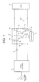
- FIG. 1 is a configuration diagram of a boost circuit according to a first embodiment of the present invention.
- the boost circuit includes a diode rectifier 2 connected to an AC power source 1 and a power factor improvement reactor 3 that is provided on the DC side of the diode rectifier 2 and is connected to one end of an output terminal of the diode rectifier 2 to improve the power factor.
- the reactor 3 improves the input power factor from the AC power source.
- the reactors 3 is connected to the positive electric potential side of the diode rectifier 2 (rectifying circuit).
- a highfrequency noise suppressing capacitor 4 Between the other end of the power factor improvement reactor 3 and the other end of the output terminal of the diode rectifier 2, arranged is a highfrequency noise suppressing capacitor 4 to suppress highfrequency noise generated from a boosting chopper circuit.
- a low-pass filter LPF is configured. Only a common mode filter that can easily filter noise on the AC side may be installed.
- two boosting reactors 5a and 5b are provided in parallel to the other end of the power factor improvement reactor 3 in the boost circuit of the embodiment.
- power devices 6a and 6b switching devices that turn on or off current flowing to each of the boosting reactors 5a and 5b are provided in series to the boosting reactors 5a and 5b, respectively.
- FSDs 7a and 7b that perform fast recovery are arranged to the boosting reactors 5a and 5b on the side opposite to the power factor improvement reactor 3.
- a current bypass diode 8 to bypass the boosting chopper circuit.
- one current detection device 9 is provided between the power devices 6a and 6b (switching devices) that turn on or off current and the other end of the diode rectifier 2. Specifically, one current detection device 9 is provided between the emitter terminal or the source terminal of each of the power devices 6a and 6b and the negative electric potential terminal of input voltage.
- the current detection device 9 employs a current sampling resistor and an amplifying circuit 9a to reduce the cost as shown in FIG. 1 . In place of the current sampling resistor, a current detection device such as a current sensor configured using hall elements may be used.
- a controller 12 of the boost circuit is configured using a semiconductor arithmetic device such as an analog circuit, a microcomputer, or a DSP (Digital Signal Processor), and processes DC voltage signals and boosting target voltage from a voltage detection device of the voltage dividing resistor 10. Further, the controller 12 generates an on/off control signal for each of the power devices 6a and 6b. In this case, voltage signals are detected by the inexpensive voltage dividing resistor 10 to reduce the cost. However, in place of the voltage dividing resistor, a device such as a DC voltage sensor may be used.
- the boosting chopper circuits are connected in parallel using two boosting reactors 5a and 5b.
- the boosting chopper circuits may be configured by arranging two or more boosting reactors in parallel according to boosting voltage and output power capacity.
- the number of parts is increased because a plurality of boosting reactors 5a and 5b are provided in parallel.
- the current is equally dispersed, and thus the current flowing to one boosting chopper circuit can be reduced.
- inexpensive general-purpose components can be used for the power devices 6a and 6b and the power factor improvement reactor 3.
- the power factor improvement reactor 3 is a large part in size, and the cost thereof is high. Thus, a significant effect of cost reduction can be realized.
- the equivalent frequency of ripple components of the entire input current is increased several times by the interleave operation of each boosting chopper, and thus the noise filter can be easily designed. It should be noted that current is equally dispersed to a plurality of boosting chopper circuits, and thus the control signal of each of the power devices 6a and 6b needs to be adjusted by detecting each current. Thus, the control by the controller 12 will be described below.
- FIG. 2 is a functional block configuration diagram of the controller 12.
- a DC voltage controller 21 calculates a current command using a difference between the DC voltage detected on the basis of the DC voltage signal from the voltage dividing resistor 10 and the boosting target voltage. Further, a ripple compensation controller 25 extracts the ripple components of the DC voltage using a device such as a bandpass filter (BPF), and creates a cancellation controlled variable to suppress the ripple. In addition, the cancellation controlled variable is added to the current command.
- BPF bandpass filter
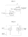
- FIG. 3 shows an internal configuration of the ripple compensation controller 25.
- the center frequency of a bandpass filter 31 is twice the frequency of the power source.
- the center frequency of the bandpass filter 31 is six times the frequency of the power source. Only the voltage ripple components are left in the output of the bandpass filter 31.
- a ripple suppressing control signal is created using a PI controller 32 so as to eliminate the voltage ripple components.
- a current controller 22 calculates a control modulation factor using the current commands from the DC voltage controller 21 and the ripple compensation controller 25 and the current signal from a current computing unit 27.
- the control modulation factor is a controlled variable to generate a PWM control signal while being compared with a carrier wave by a PWM controller 24a.
- a current signal from the current detection device 9 is converted from analog to digital by an A/D and current separator 26, and is divided as current flowing to each of the power devices 6a and 6b using an interleave switching signal.
- FIG. 4 shows a processing configuration of the A/D and current separator 26. Further, the start timing of an A/D converter is set in accordance with on-state periods of each of the power devices 6a and 6b as shown in FIG. 6 . In this case, the on-state periods mutually appear due to the interleave operation of each of the power devices 6a and 6b. Thus, even a current detection device with one sampling and hold circuit or an A/D converter can detect the current flowing to each of the power devices 6a and 6b.
- the current computing unit 27 calculates the sum and difference of two kinds of current detected by the A/D and current separator 26.
- FIG. 5 is a functional block diagram of a modulation factor adjuster 23 to equally control the current of each boosting chopper.
- the difference of current calculated by the current computing unit 27 calculates an adjusting gain through a PI controller 51. Further, each modulation factor is adjusted using a multiplier 52 in addition and subtraction processes between the adjusting gain and 1.
- the PWM controllers 24a and 24b generate a PWM (Pulse Width Modulation) control signal on the basis of a comparison between each modulation factor and carrier waves (triangular wave or sawtooth wave) from a carrier wave generator 28, and output an on/off control signal for each power device in accordance with a switching signal from a counter 29.
- PWM Pulse Width Modulation
- FIG. 6 shows waveforms of the current and control signal of each power device, the current of the current detection resistor 9, and the detected current.
- the start timing of converting from analog to digital is set at the on-state period of each power device. Specifically, it is determined from which of the plurality of power devices 6a and 6b the current flowing to the single current detection resistor 9 has come in a sampling process of the on-state period of each of the power devices 6a and 6b. Then, the current flowing to each of the power devices 6a and 6b is detected, and the on width of each power device is adjusted so as to substantially equalize the current of each power device.
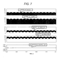
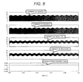
- FIG. 7 and FIG. 8 show waveforms of the current of the power devices, the boosting reactors, and the equal control gain when the current equal control is on and off.
- the equal control gain is automatically adjusted by the current equal control, and the current of each power device can be substantially similarly controlled. Accordingly, the current detection circuit and control can be simplified, and thus a boost circuit, a motor driving module, and a refrigerating apparatus at low cost and with high efficiency can be provided.
- FIG. 9 shows a configuration of a motor driving apparatus according to a second embodiment of the present invention.
- the rectifying and boost circuit parts that convert from AC to DC are the same as those shown in FIG. 1 .
- An inverter 16 is used on the DC output side of the boost circuit to drive a motor 17.
- a controller 12a generates PWM control signals for the boost circuit and the inverter to control the DC voltage and the motor. Using information such as the revolutions and current of the motor and the output voltage or the modulation factor (the ratio of the output voltage to the DC voltage) of the inverter, the optimum boosting target voltage is calculated to control the DC voltage.
- the boost circuit is controlled using the control configuration of FIG. 2 described in the first embodiment.
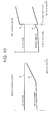
- FIG. 10 shows an image of adjusting the DC voltage using the boost circuit in the motor driving apparatus.
- the operation of the boost circuit is stopped in the middle to low speed operation range, and the motor is controlled only by the PWM control of the inverter.
- the boost circuit is operated in the high speed operation range to adjust the DC voltage, and the current of the motor is reduced by the boosting control and the PWM control of the inverter. Further, the boosting voltage target value is adjusted to improve the efficiency of the entire system and to reduce the current of the motor.
- the adjusting method is realized by preparing, for example, a relation table between preliminarily-set boosting voltage target values and the rotating speed of motor.
- the motor driving apparatus of the embodiment a motor with higher induced voltage designed can be adopted as compared to a case without the boost circuit, and accordingly the current of the motor and the loss of the inverter can be reduced in the middle to low speed range.
- the current of the inverter can be reduced by the boosting operation in the high speed range, and thus a lower-rating semiconductor switching device can be adopted.
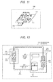
- FIG. 11 is an external diagram of a motor driving module 200 according to a third embodiment of the present invention, and shows one configuration of a finished product.
- the module 200 is a motor driving module obtained by mounting a semiconductor switching device 202 on a substrate 201, and the boost circuit, the voltage current detection circuit, the controller, the inverter circuit, and the like illustrated in FIG. 10 are mounted on the substrate 201.
- the apparatus can be downsized by modularization, and the cost of the apparatus can be reduced.
- the module means a "normalized constitutional unit", and is configured using separable hardware/software components.
- the above-described components are preferably configured on the same substrate in manufacturing.
- the substrate is not limited to one substrate. Accordingly, the above-described components may be configured on a plurality of circuit substrates incorporated in the housing.
- the cost and volume of the entire product can be reduced, and thus the versatility and convenience of the motor driving system using the module of the embodiment can be improved.
- FIG. 12 shows a fourth embodiment of the present invention, that is, a configuration diagram of a refrigerating apparatus such as an air conditioner or refrigerator that drives a compressor motor using the motor driving module.
- a refrigerating apparatus 300 is an apparatus to condition temperatures, and is configured using heat exchangers 301 and 302, fans 303 and 304 that feed air to these heat exchangers, a compressor 305 that compresses and circulates a refrigerant, a pipe 306 in which the refrigerant flows, and a motor driving unit 307.
- a compressor motor 308 is arranged inside the compressor 305 using a permanent magnet synchronous motor or a three-phase induction motor.
- the motor driving unit 307 converts the AC power source to DC, and supplies the DC power to a motor driving inverter to drive the motor.
- the boosting control of the DC voltage can be performed, and the motor can be driven with higher efficiency and in a wider range.
- the improvement of the efficiency and the cost reduction of the refrigerating apparatus can be realized.
Landscapes
- Engineering & Computer Science (AREA)
- Power Engineering (AREA)
- Dc-Dc Converters (AREA)
- Rectifiers (AREA)
- Control Of Ac Motors In General (AREA)
Abstract
Description
- The present invention relates to a rectifier that converts AC to DC, a boost circuit, a motor driving module, and a refrigerating apparatus.
- A motor driving system configured using a rectifier that converts an AC power source to DC and an inverter circuit that converts DC to AC has been widely used in home appliance and industrial equipment. In order to improve the annual performance factor (APF), it has been desirable for a refrigerating apparatus such as an air conditioner to improve the efficiency in the middle to low speed operation range where the motor is mostly operated. Therefore, the motor tends to be designed so that the motor induced voltage (back electromotive force) becomes high in recent years.
- However, since the motor induced voltage (back electromotive force) is proportional to the rotating speed of a motor, the output voltage of an inverter becomes lower than the induced voltage of the motor by limitation of DC voltage in the range of high-speed operation, and the motor cannot be normally driven in some cases. As a conventional countermeasure, there is a method such as field-weakening control. However, as shown in
FIG. 10 , the losses of the motor and inverter are increased according to an increase in the reactive current of the motor, and the total efficiency of the system is deteriorated. Instead, it is effective that the DC voltage is boosted to increase the output voltage of the inverter in the case where the output voltage of the inverter is insufficient. - A circuit configuration of boosting after converting AC voltage to DC has been developed from a long time ago, and a plurality of methods have been proposed. For example, using a three-phase PWM converter configured using six semiconductor power devices, the harmonic reduction of input current and the boosting control of output DC voltage can be performed. However, a plurality of semiconductor power devices and complicated control devices are necessary, and thus the cost of the apparatus is significantly increased. The product cost is considered to be important for consumer and industrial apparatuses such as air conditioners and general-purpose inverters, and thus it has been desirable to use inexpensive boosting devices.
- Further, as a simple boosting device, for example, Japanese Patent No.
4937281 2010-233439 - In the boost circuit described in Japanese Patent No.
4937281 - As described in Japanese Unexamined Patent Application Publication No.
2010-233439 - An object of the present invention is to provide a boost circuit, a motor driving module, and a refrigerating apparatus that detect the current of each power device using one current detection device, and adjust the on width of each power device to substantially equalize the current of each power device.
- In order to address the above-described problems, the present invention provides a boost circuit including: a rectifying circuit for an AC power source; a plurality of reactors that are connected in parallel to the positive electric potential side of the rectifying circuit; a plurality of power devices that are connected in series to the plurality of reactors to turn on or off current; a single resistor that is connected between the plurality of power devices and the negative electric potential side of the rectifying circuit; and/or a control unit alternately controls the plurality of power devices so that the current flowing to the plurality of power devices is substantially equalized.
- According to the present invention, the current of each power device is detected using one current detection device, and the on width of each power device is adjusted, so that the current of each power device can be substantially equalized. Therefore, the current detection circuit and control can be simplified, and thus it is possible to provide a boost circuit, a motor driving module, and a refrigerating apparatus at low cost and with high efficiency. The other configurations, actions, and effects of the present invention will be described in embodiments shown below.
-
-
FIG. 1 is a configuration diagram of a boost circuit according to one embodiment of the present invention; -
FIG. 2 is a functional block configuration diagram of a control unit of the boost circuit according to one embodiment of the present invention; -
FIG. 3 is a configuration diagram of a ripple compensation controller of the control unit of the boost circuit according to one embodiment of the present invention; -
FIG. 4 is a configuration diagram of an A/D and current separator of the control unit of the boost circuit according to one embodiment of the present invention; -
FIG. 5 is a configuration diagram of a modulation factor adjuster of the control unit of the boost circuit according to one embodiment of the present invention; -
FIG. 6 is an explanatory diagram of a current detection method of the boost circuit according to one embodiment of the present invention; -
FIG. 7 is an explanatory diagram of a current equalization control effect of the boost circuit according to one embodiment of the present invention; -
FIG. 8 is an explanatory diagram of the current equalization control effect of the boost circuit according to one embodiment of the present invention; -
FIG. 9 is a circuit configuration diagram of a motor driving module according to one embodiment of the present invention; -
FIG. 10 is an explanatory diagram of a boosting effect of the motor driving module according to one embodiment of the present invention; -
FIG. 11 is an external diagram of the motor driving module according to one embodiment of the present invention; and -
FIG. 12 is a configuration diagram of a refrigerating apparatus according to one embodiment of the present invention. - Hereinafter, embodiments of the present invention will be described using the drawings.
-
FIG. 1 is a configuration diagram of a boost circuit according to a first embodiment of the present invention. The boost circuit includes adiode rectifier 2 connected to anAC power source 1 and a powerfactor improvement reactor 3 that is provided on the DC side of thediode rectifier 2 and is connected to one end of an output terminal of thediode rectifier 2 to improve the power factor. Thereactor 3 improves the input power factor from the AC power source. Thereactors 3 is connected to the positive electric potential side of the diode rectifier 2 (rectifying circuit). Between the other end of the powerfactor improvement reactor 3 and the other end of the output terminal of thediode rectifier 2, arranged is a highfrequencynoise suppressing capacitor 4 to suppress highfrequency noise generated from a boosting chopper circuit. Specifically, a low-pass filter (LPF) is configured. Only a common mode filter that can easily filter noise on the AC side may be installed. - In addition, two
boosting reactors factor improvement reactor 3 in the boost circuit of the embodiment. Further,power devices boosting reactors boosting reactors - Fast recovery diodes (FRDs) 7a and 7b that perform fast recovery are arranged to the
boosting reactors factor improvement reactor 3. Between the input side and the output side of the boosting chopper circuit configured by including theboosting reactors power devices current bypass diode 8 to bypass the boosting chopper circuit. - When the operation of the boost circuit stops, current of the
boosting reactors current bypass diode 8 that is a general-purpose rectifying diode. Thus, a conduction loss when the boosting operation stops can be reduced. - In the embodiment, one
current detection device 9 is provided between thepower devices diode rectifier 2. Specifically, onecurrent detection device 9 is provided between the emitter terminal or the source terminal of each of thepower devices current detection device 9 employs a current sampling resistor and an amplifyingcircuit 9a to reduce the cost as shown inFIG. 1 . In place of the current sampling resistor, a current detection device such as a current sensor configured using hall elements may be used. - Between the output side of the fast recovery diodes (FRDs) 7a and 7b and the other end of the
diode rectifier 2, provided is avoltage dividing resistor 10 for voltage detection, and asmoothing capacitor 11 for output voltage is provided in parallel to thevoltage dividing resistor 10 for voltage detection. Acontroller 12 of the boost circuit is configured using a semiconductor arithmetic device such as an analog circuit, a microcomputer, or a DSP (Digital Signal Processor), and processes DC voltage signals and boosting target voltage from a voltage detection device of thevoltage dividing resistor 10. Further, thecontroller 12 generates an on/off control signal for each of thepower devices voltage dividing resistor 10 to reduce the cost. However, in place of the voltage dividing resistor, a device such as a DC voltage sensor may be used. - In the embodiment, the boosting chopper circuits are connected in parallel using two boosting
reactors - In the embodiment as described above, the number of parts is increased because a plurality of boosting
reactors power devices factor improvement reactor 3. Especially, the powerfactor improvement reactor 3 is a large part in size, and the cost thereof is high. Thus, a significant effect of cost reduction can be realized. - Further, the equivalent frequency of ripple components of the entire input current is increased several times by the interleave operation of each boosting chopper, and thus the noise filter can be easily designed. It should be noted that current is equally dispersed to a plurality of boosting chopper circuits, and thus the control signal of each of the
power devices controller 12 will be described below. -
FIG. 2 is a functional block configuration diagram of thecontroller 12. - Specifically, a
DC voltage controller 21 calculates a current command using a difference between the DC voltage detected on the basis of the DC voltage signal from thevoltage dividing resistor 10 and the boosting target voltage. Further, aripple compensation controller 25 extracts the ripple components of the DC voltage using a device such as a bandpass filter (BPF), and creates a cancellation controlled variable to suppress the ripple. In addition, the cancellation controlled variable is added to the current command. -
FIG. 3 shows an internal configuration of theripple compensation controller 25. In the case of a single-phase power source, the center frequency of abandpass filter 31 is twice the frequency of the power source. In the case of a three-phase power source, the center frequency of thebandpass filter 31 is six times the frequency of the power source. Only the voltage ripple components are left in the output of thebandpass filter 31. A ripple suppressing control signal is created using aPI controller 32 so as to eliminate the voltage ripple components. - A
current controller 22 calculates a control modulation factor using the current commands from theDC voltage controller 21 and theripple compensation controller 25 and the current signal from acurrent computing unit 27. The control modulation factor is a controlled variable to generate a PWM control signal while being compared with a carrier wave by aPWM controller 24a. - A current signal from the
current detection device 9 is converted from analog to digital by an A/D andcurrent separator 26, and is divided as current flowing to each of thepower devices -
FIG. 4 shows a processing configuration of the A/D andcurrent separator 26. Further, the start timing of an A/D converter is set in accordance with on-state periods of each of thepower devices FIG. 6 . In this case, the on-state periods mutually appear due to the interleave operation of each of thepower devices power devices current computing unit 27 calculates the sum and difference of two kinds of current detected by the A/D andcurrent separator 26. -
FIG. 5 is a functional block diagram of amodulation factor adjuster 23 to equally control the current of each boosting chopper. The difference of current calculated by thecurrent computing unit 27 calculates an adjusting gain through aPI controller 51. Further, each modulation factor is adjusted using amultiplier 52 in addition and subtraction processes between the adjusting gain and 1. - Finally, the
PWM controllers carrier wave generator 28, and output an on/off control signal for each power device in accordance with a switching signal from acounter 29. -
FIG. 6 shows waveforms of the current and control signal of each power device, the current of thecurrent detection resistor 9, and the detected current. The start timing of converting from analog to digital is set at the on-state period of each power device. Specifically, it is determined from which of the plurality ofpower devices current detection resistor 9 has come in a sampling process of the on-state period of each of thepower devices power devices -
FIG. 7 andFIG. 8 show waveforms of the current of the power devices, the boosting reactors, and the equal control gain when the current equal control is on and off. As shown inFIG. 8 , according to the control of the boost circuit of the embodiment as described above, the equal control gain is automatically adjusted by the current equal control, and the current of each power device can be substantially similarly controlled. Accordingly, the current detection circuit and control can be simplified, and thus a boost circuit, a motor driving module, and a refrigerating apparatus at low cost and with high efficiency can be provided. -
FIG. 9 shows a configuration of a motor driving apparatus according to a second embodiment of the present invention. The rectifying and boost circuit parts that convert from AC to DC are the same as those shown inFIG. 1 . Aninverter 16 is used on the DC output side of the boost circuit to drive amotor 17. Acontroller 12a generates PWM control signals for the boost circuit and the inverter to control the DC voltage and the motor. Using information such as the revolutions and current of the motor and the output voltage or the modulation factor (the ratio of the output voltage to the DC voltage) of the inverter, the optimum boosting target voltage is calculated to control the DC voltage. The boost circuit is controlled using the control configuration ofFIG. 2 described in the first embodiment. -
FIG. 10 shows an image of adjusting the DC voltage using the boost circuit in the motor driving apparatus. The operation of the boost circuit is stopped in the middle to low speed operation range, and the motor is controlled only by the PWM control of the inverter. The boost circuit is operated in the high speed operation range to adjust the DC voltage, and the current of the motor is reduced by the boosting control and the PWM control of the inverter. Further, the boosting voltage target value is adjusted to improve the efficiency of the entire system and to reduce the current of the motor. The adjusting method is realized by preparing, for example, a relation table between preliminarily-set boosting voltage target values and the rotating speed of motor. - Thus, if the motor driving apparatus of the embodiment is used, a motor with higher induced voltage designed can be adopted as compared to a case without the boost circuit, and accordingly the current of the motor and the loss of the inverter can be reduced in the middle to low speed range. The current of the inverter can be reduced by the boosting operation in the high speed range, and thus a lower-rating semiconductor switching device can be adopted.
-
FIG. 11 is an external diagram of amotor driving module 200 according to a third embodiment of the present invention, and shows one configuration of a finished product. Themodule 200 is a motor driving module obtained by mounting asemiconductor switching device 202 on asubstrate 201, and the boost circuit, the voltage current detection circuit, the controller, the inverter circuit, and the like illustrated inFIG. 10 are mounted on thesubstrate 201. The apparatus can be downsized by modularization, and the cost of the apparatus can be reduced. It should be noted that the module means a "normalized constitutional unit", and is configured using separable hardware/software components. Further, the above-described components are preferably configured on the same substrate in manufacturing. However, the substrate is not limited to one substrate. Accordingly, the above-described components may be configured on a plurality of circuit substrates incorporated in the housing. - According to the embodiment, the cost and volume of the entire product can be reduced, and thus the versatility and convenience of the motor driving system using the module of the embodiment can be improved.
-
FIG. 12 shows a fourth embodiment of the present invention, that is, a configuration diagram of a refrigerating apparatus such as an air conditioner or refrigerator that drives a compressor motor using the motor driving module. A refrigerating apparatus 300 is an apparatus to condition temperatures, and is configured usingheat exchangers fans compressor 305 that compresses and circulates a refrigerant, apipe 306 in which the refrigerant flows, and amotor driving unit 307. It should be noted that acompressor motor 308 is arranged inside thecompressor 305 using a permanent magnet synchronous motor or a three-phase induction motor. Themotor driving unit 307 converts the AC power source to DC, and supplies the DC power to a motor driving inverter to drive the motor. - Using the motor driving module of the third embodiment, the boosting control of the DC voltage can be performed, and the motor can be driven with higher efficiency and in a wider range. Thus, the improvement of the efficiency and the cost reduction of the refrigerating apparatus can be realized.
- Features, components and specific details of the structures of the above-described embodiments may be exchanged or combined to form further embodiments optimized for the respective application. As far as those modifications are apparent for an expert skilled in the art they shall be disclosed implicitly by the above description without specifying explicitly every possible combination.
Claims (6)
- A boost circuit (2) comprising:a rectifying circuit connected to an AC power source (1) ;a plurality of reactors that are connected in parallel to the positive electric potential side of the rectifying circuit (2);a plurality of power devices (6a, 6b) that are connected in series to the plurality of reactors to turn on or off current;a single resistor that is connected between the plurality of power devices (6a, 6b) and the negative electric potential side of the rectifying circuit (2); anda control unit (12) that determines from which of plurality of power devices (6a, 6b) the current flowing to the single current detection resistor (9) has come, and alternately controls the plurality of power devices (6a, 6b) so that the current flowing to the plurality of power devices (6a, 6b) is substantially equalized.
- The boost circuit according to claim 1, wherein
the current of each power device (6a, 6b) is detected in a sampling process of the on section of each power device (6a, 6b) using detection devices such as a sampling and hold circuit and an A/D converter. - The boost circuit according to claim 1, wherein
a difference between current values detected by the power devices (6a, 6b) is calculated so as to substantially equalize the current of each power device (6a, 6b), and is input into a feedback controller to adjust the on width of each power device (6a, 6b). - The boost circuit according to claim 1 or 2, wherein
the output voltage of the boost circuit is detected to separate ripple components using a device such as a bandpass filter (31), and the ripple components of the output voltage are suppressed by adjusting an on/off control signal of each power device (6a, 6b). - A motor driving module having an inverter (16) that drives a motor by controlling DC voltage, wherein
the boost circuit according to at least one of claims 1 to 4 is provided on the input side of the inverter (16), and the control unit (12) determines whether to stop the start of the boost circuit and adjusts the output voltage using at least one piece of information of the output voltage, the output power, and the control modulation factor (ratio of output voltage to DC voltage) of the inverter (16), the frequency of a motor (17), and the current of the motor (17). - A refrigerating apparatus comprising:a heat exchanger (301, 302);a fan (303, 304) that feeds air to the heat exchanger (301, 302);a compressor (305) that compresses and circulates a refrigerant; andan inverter (16) that drives a motor (17) for the compressor (305), whereinthe boost circuit according to at least one of claims 1 to 4 is provided on the input side of the inverter (.16).
Applications Claiming Priority (1)
| Application Number | Priority Date | Filing Date | Title |
|---|---|---|---|
| JP2014132025A JP6349165B2 (en) | 2014-06-27 | 2014-06-27 | Booster circuit, motor drive module and refrigeration equipment |
Publications (2)
| Publication Number | Publication Date |
|---|---|
| EP2961051A1 true EP2961051A1 (en) | 2015-12-30 |
| EP2961051B1 EP2961051B1 (en) | 2019-02-06 |
Family
ID=53491336
Family Applications (1)
| Application Number | Title | Priority Date | Filing Date |
|---|---|---|---|
| EP15173906.7A Active EP2961051B1 (en) | 2014-06-27 | 2015-06-25 | Boost circuit, motor driving module, and refrigerating apparatus |
Country Status (3)
| Country | Link |
|---|---|
| EP (1) | EP2961051B1 (en) |
| JP (1) | JP6349165B2 (en) |
| CN (1) | CN105305820A (en) |
Cited By (3)
| Publication number | Priority date | Publication date | Assignee | Title |
|---|---|---|---|---|
| CN110729899A (en) * | 2019-11-01 | 2020-01-24 | 山东大学 | Wide-input wide-output three-phase high-gain direct current converter and control method |
| CN112803868A (en) * | 2020-12-30 | 2021-05-14 | 宁波奥克斯电气股份有限公司 | Inverter output voltage control method and device, inverter and air conditioner |
| EP3799294A4 (en) * | 2018-11-28 | 2021-12-15 | Qingdao Haier Air-Conditioning Electronic Co., Ltd | COMPRESSOR, AIR CONDITIONER, STORAGE STORAGE PROCESS AND SUPPORT CONTROL UNIT |
Families Citing this family (7)
| Publication number | Priority date | Publication date | Assignee | Title |
|---|---|---|---|---|
| CN106655950B (en) * | 2016-11-24 | 2019-08-27 | 中国航空工业集团公司金城南京机电液压工程研究中心 | A kind of adjustable electric machine control system of voltage |
| JP2018166376A (en) * | 2017-03-28 | 2018-10-25 | 新電元工業株式会社 | Switching power supply device and control method thereof |
| CN107733250A (en) * | 2017-11-11 | 2018-02-23 | 湖南众源电子科技有限公司 | A kind of dc source based on air-conditioning system |
| US11831230B2 (en) | 2019-02-25 | 2023-11-28 | Mitsubishi Electric Corporation | Power supply, motor driver, blower, compressor, and air conditioner |
| CN111490673B (en) * | 2020-05-21 | 2021-02-09 | 四川虹美智能科技有限公司 | Output voltage control method and device |
| CN112713771A (en) * | 2020-12-23 | 2021-04-27 | 浙江飞越机电有限公司 | Power supply circuit of direct-current brushless motor with ultra-wide input voltage |
| KR20220121044A (en) | 2021-02-24 | 2022-08-31 | 주식회사 히타치엘지 데이터 스토리지 코리아 | Wireless charging device and its control method |
Citations (5)
| Publication number | Priority date | Publication date | Assignee | Title |
|---|---|---|---|---|
| US5889663A (en) * | 1997-05-14 | 1999-03-30 | Fuji Electric Co., Ltd. | Circuit for balancing steady-state currents of switching devices in electric power converter |
| JP2010233439A (en) | 2009-03-03 | 2010-10-14 | Toshiba Corp | Power supply control device and power supply device using the same |
| JP4937281B2 (en) | 2009-01-16 | 2012-05-23 | 三菱電機株式会社 | Motor drive control device, compressor, blower, air conditioner, refrigerator or freezer |
| US20130342139A1 (en) * | 2011-04-08 | 2013-12-26 | Mitsubishi Electric Corporation | Power converting device, motor driving device, and refrigerating and air-conditioning apparatus |
| US20140169049A1 (en) * | 2012-12-13 | 2014-06-19 | Power Systems Technologies, Ltd. | Controller for a Power Converter and Method of Operating the Same |
Family Cites Families (5)
| Publication number | Priority date | Publication date | Assignee | Title |
|---|---|---|---|---|
| JP4799512B2 (en) * | 2007-08-31 | 2011-10-26 | 三菱電機株式会社 | Power converter and air conditioner using the same |
| JP2009060759A (en) * | 2007-09-03 | 2009-03-19 | Toyota Motor Corp | Power supply system and charge control method thereof |
| CN102170221B (en) * | 2011-04-20 | 2013-11-06 | 上海交通大学 | Interleaved power factor corrector with approximate open-loop control |
| JP5804763B2 (en) * | 2011-05-02 | 2015-11-04 | 三菱電機株式会社 | Control device for air conditioner |
| US9077243B2 (en) * | 2012-01-31 | 2015-07-07 | Analog Devices, Inc. | Current-balancing in interleaved circuit phases using a parameter common to the phases |
-
2014
- 2014-06-27 JP JP2014132025A patent/JP6349165B2/en active Active
-
2015
- 2015-06-25 EP EP15173906.7A patent/EP2961051B1/en active Active
- 2015-06-26 CN CN201510362024.6A patent/CN105305820A/en active Pending
Patent Citations (5)
| Publication number | Priority date | Publication date | Assignee | Title |
|---|---|---|---|---|
| US5889663A (en) * | 1997-05-14 | 1999-03-30 | Fuji Electric Co., Ltd. | Circuit for balancing steady-state currents of switching devices in electric power converter |
| JP4937281B2 (en) | 2009-01-16 | 2012-05-23 | 三菱電機株式会社 | Motor drive control device, compressor, blower, air conditioner, refrigerator or freezer |
| JP2010233439A (en) | 2009-03-03 | 2010-10-14 | Toshiba Corp | Power supply control device and power supply device using the same |
| US20130342139A1 (en) * | 2011-04-08 | 2013-12-26 | Mitsubishi Electric Corporation | Power converting device, motor driving device, and refrigerating and air-conditioning apparatus |
| US20140169049A1 (en) * | 2012-12-13 | 2014-06-19 | Power Systems Technologies, Ltd. | Controller for a Power Converter and Method of Operating the Same |
Cited By (6)
| Publication number | Priority date | Publication date | Assignee | Title |
|---|---|---|---|---|
| EP3799294A4 (en) * | 2018-11-28 | 2021-12-15 | Qingdao Haier Air-Conditioning Electronic Co., Ltd | COMPRESSOR, AIR CONDITIONER, STORAGE STORAGE PROCESS AND SUPPORT CONTROL UNIT |
| US11480374B2 (en) | 2018-11-28 | 2022-10-25 | Qingdao Haier Air-Conditioning Electronic Co., Ltd. | Device and method for field weakening control of compressor, air conditioner and storage medium |
| CN110729899A (en) * | 2019-11-01 | 2020-01-24 | 山东大学 | Wide-input wide-output three-phase high-gain direct current converter and control method |
| CN110729899B (en) * | 2019-11-01 | 2020-08-04 | 山东大学 | Wide-input wide-output three-phase high-gain direct current converter and control method |
| CN112803868A (en) * | 2020-12-30 | 2021-05-14 | 宁波奥克斯电气股份有限公司 | Inverter output voltage control method and device, inverter and air conditioner |
| CN112803868B (en) * | 2020-12-30 | 2022-07-12 | 宁波奥克斯电气股份有限公司 | Inverter output voltage control method and device, inverter and air conditioner |
Also Published As
| Publication number | Publication date |
|---|---|
| EP2961051B1 (en) | 2019-02-06 |
| CN105305820A (en) | 2016-02-03 |
| JP2016012952A (en) | 2016-01-21 |
| JP6349165B2 (en) | 2018-06-27 |
Similar Documents
| Publication | Publication Date | Title |
|---|---|---|
| EP2961051B1 (en) | Boost circuit, motor driving module, and refrigerating apparatus | |
| JP5119222B2 (en) | Converter device, motor driving module, and refrigeration device | |
| CN106464172B (en) | Compressor drive device, compressor having the same, and refrigeration cycle device having the same | |
| JP5558530B2 (en) | Motor drive control device, compressor, blower, air conditioner, refrigerator or freezer | |
| JP6614825B2 (en) | Power conversion device, motor drive device, refrigeration device | |
| US20190052210A1 (en) | Motor drive device and refrigeration equipment | |
| US9960703B2 (en) | DC power-supply device and refrigeration-cycle application device including the same | |
| JP5557660B2 (en) | Power conversion device and equipment using the same | |
| EP2096742B1 (en) | Power factor correction circuit for air conditioning equipment | |
| US10003287B2 (en) | Magnet degradation and damage controls and diagnostics for permanent magnet motors | |
| JP5518097B2 (en) | Converter device, motor drive module, and refrigeration equipment | |
| EP3182574B1 (en) | Converter unit, drive controller, motor, and compressor | |
| US20190097559A1 (en) | Power conversion device, motor drive device, and refrigerator using same | |
| WO2014103745A1 (en) | Booster circuit, motor drive module and refrigerating equipment | |
| CN109075695A (en) | For DC to the AC of variable-speed motor and high-speed motor power inverter | |
| JP2003348892A (en) | Control unit for a plurality of motors, power converter, inverter module and converter module | |
| JP4887216B2 (en) | Power converter for driving refrigeration cycle compressor and refrigeration system using the same | |
| JP5975830B2 (en) | Motor control device and refrigeration equipment using the same | |
| JP2012151993A (en) | Electric power conversion system and rotary machine drive system using the same | |
| CN114128131A (en) | Power conversion device | |
| US9654049B2 (en) | Variable frequency drive active harmonic mitigation controls and diagnostics | |
| JP2015023785A (en) | Power conversion device and air conditioner | |
| WO2025069182A1 (en) | Power conversion device, electric-motor drive device, and apparatus in which a cryocooling cycle is applied | |
| EP2949037A1 (en) | Variable frequency drive active harmonic mitigation controls and diagnostics | |
| KR20160086695A (en) | Power converter and air conditioner including the same |
Legal Events
| Date | Code | Title | Description |
|---|---|---|---|
| PUAI | Public reference made under article 153(3) epc to a published international application that has entered the european phase |
Free format text: ORIGINAL CODE: 0009012 |
|
| 17P | Request for examination filed |
Effective date: 20150814 |
|
| AK | Designated contracting states |
Kind code of ref document: A1 Designated state(s): AL AT BE BG CH CY CZ DE DK EE ES FI FR GB GR HR HU IE IS IT LI LT LU LV MC MK MT NL NO PL PT RO RS SE SI SK SM TR |
|
| AX | Request for extension of the european patent |
Extension state: BA ME |
|
| RAP1 | Party data changed (applicant data changed or rights of an application transferred) |
Owner name: JOHNSON CONTROLS-HITACHI AIR CONDITIONING TECHNOLO |
|
| RAP1 | Party data changed (applicant data changed or rights of an application transferred) |
Owner name: HITACHI-JOHNSON CONTROLS AIR CONDITIONING, INC. |
|
| GRAP | Despatch of communication of intention to grant a patent |
Free format text: ORIGINAL CODE: EPIDOSNIGR1 |
|
| STAA | Information on the status of an ep patent application or granted ep patent |
Free format text: STATUS: GRANT OF PATENT IS INTENDED |
|
| GRAJ | Information related to disapproval of communication of intention to grant by the applicant or resumption of examination proceedings by the epo deleted |
Free format text: ORIGINAL CODE: EPIDOSDIGR1 |
|
| STAA | Information on the status of an ep patent application or granted ep patent |
Free format text: STATUS: REQUEST FOR EXAMINATION WAS MADE |
|
| GRAP | Despatch of communication of intention to grant a patent |
Free format text: ORIGINAL CODE: EPIDOSNIGR1 |
|
| RIC1 | Information provided on ipc code assigned before grant |
Ipc: H02M 3/158 20060101AFI20180706BHEP |
|
| STAA | Information on the status of an ep patent application or granted ep patent |
Free format text: STATUS: GRANT OF PATENT IS INTENDED |
|
| INTG | Intention to grant announced |
Effective date: 20180727 |
|
| INTG | Intention to grant announced |
Effective date: 20180816 |
|
| GRAS | Grant fee paid |
Free format text: ORIGINAL CODE: EPIDOSNIGR3 |
|
| GRAA | (expected) grant |
Free format text: ORIGINAL CODE: 0009210 |
|
| STAA | Information on the status of an ep patent application or granted ep patent |
Free format text: STATUS: THE PATENT HAS BEEN GRANTED |
|
| AK | Designated contracting states |
Kind code of ref document: B1 Designated state(s): AL AT BE BG CH CY CZ DE DK EE ES FI FR GB GR HR HU IE IS IT LI LT LU LV MC MK MT NL NO PL PT RO RS SE SI SK SM TR |
|
| REG | Reference to a national code |
Ref country code: GB Ref legal event code: FG4D |
|
| REG | Reference to a national code |
Ref country code: CH Ref legal event code: EP Ref country code: AT Ref legal event code: REF Ref document number: 1095484 Country of ref document: AT Kind code of ref document: T Effective date: 20190215 |
|
| REG | Reference to a national code |
Ref country code: IE Ref legal event code: FG4D |
|
| REG | Reference to a national code |
Ref country code: DE Ref legal event code: R096 Ref document number: 602015024273 Country of ref document: DE |
|
| REG | Reference to a national code |
Ref country code: NL Ref legal event code: MP Effective date: 20190206 |
|
| REG | Reference to a national code |
Ref country code: LT Ref legal event code: MG4D |
|
| PG25 | Lapsed in a contracting state [announced via postgrant information from national office to epo] |
Ref country code: PT Free format text: LAPSE BECAUSE OF FAILURE TO SUBMIT A TRANSLATION OF THE DESCRIPTION OR TO PAY THE FEE WITHIN THE PRESCRIBED TIME-LIMIT Effective date: 20190606 Ref country code: SE Free format text: LAPSE BECAUSE OF FAILURE TO SUBMIT A TRANSLATION OF THE DESCRIPTION OR TO PAY THE FEE WITHIN THE PRESCRIBED TIME-LIMIT Effective date: 20190206 Ref country code: NO Free format text: LAPSE BECAUSE OF FAILURE TO SUBMIT A TRANSLATION OF THE DESCRIPTION OR TO PAY THE FEE WITHIN THE PRESCRIBED TIME-LIMIT Effective date: 20190506 Ref country code: FI Free format text: LAPSE BECAUSE OF FAILURE TO SUBMIT A TRANSLATION OF THE DESCRIPTION OR TO PAY THE FEE WITHIN THE PRESCRIBED TIME-LIMIT Effective date: 20190206 Ref country code: NL Free format text: LAPSE BECAUSE OF FAILURE TO SUBMIT A TRANSLATION OF THE DESCRIPTION OR TO PAY THE FEE WITHIN THE PRESCRIBED TIME-LIMIT Effective date: 20190206 Ref country code: LT Free format text: LAPSE BECAUSE OF FAILURE TO SUBMIT A TRANSLATION OF THE DESCRIPTION OR TO PAY THE FEE WITHIN THE PRESCRIBED TIME-LIMIT Effective date: 20190206 |
|
| REG | Reference to a national code |
Ref country code: AT Ref legal event code: MK05 Ref document number: 1095484 Country of ref document: AT Kind code of ref document: T Effective date: 20190206 |
|
| PG25 | Lapsed in a contracting state [announced via postgrant information from national office to epo] |
Ref country code: BG Free format text: LAPSE BECAUSE OF FAILURE TO SUBMIT A TRANSLATION OF THE DESCRIPTION OR TO PAY THE FEE WITHIN THE PRESCRIBED TIME-LIMIT Effective date: 20190506 Ref country code: GR Free format text: LAPSE BECAUSE OF FAILURE TO SUBMIT A TRANSLATION OF THE DESCRIPTION OR TO PAY THE FEE WITHIN THE PRESCRIBED TIME-LIMIT Effective date: 20190507 Ref country code: IS Free format text: LAPSE BECAUSE OF FAILURE TO SUBMIT A TRANSLATION OF THE DESCRIPTION OR TO PAY THE FEE WITHIN THE PRESCRIBED TIME-LIMIT Effective date: 20190606 Ref country code: HR Free format text: LAPSE BECAUSE OF FAILURE TO SUBMIT A TRANSLATION OF THE DESCRIPTION OR TO PAY THE FEE WITHIN THE PRESCRIBED TIME-LIMIT Effective date: 20190206 Ref country code: LV Free format text: LAPSE BECAUSE OF FAILURE TO SUBMIT A TRANSLATION OF THE DESCRIPTION OR TO PAY THE FEE WITHIN THE PRESCRIBED TIME-LIMIT Effective date: 20190206 Ref country code: RS Free format text: LAPSE BECAUSE OF FAILURE TO SUBMIT A TRANSLATION OF THE DESCRIPTION OR TO PAY THE FEE WITHIN THE PRESCRIBED TIME-LIMIT Effective date: 20190206 |
|
| PG25 | Lapsed in a contracting state [announced via postgrant information from national office to epo] |
Ref country code: RO Free format text: LAPSE BECAUSE OF FAILURE TO SUBMIT A TRANSLATION OF THE DESCRIPTION OR TO PAY THE FEE WITHIN THE PRESCRIBED TIME-LIMIT Effective date: 20190206 Ref country code: IT Free format text: LAPSE BECAUSE OF FAILURE TO SUBMIT A TRANSLATION OF THE DESCRIPTION OR TO PAY THE FEE WITHIN THE PRESCRIBED TIME-LIMIT Effective date: 20190206 Ref country code: EE Free format text: LAPSE BECAUSE OF FAILURE TO SUBMIT A TRANSLATION OF THE DESCRIPTION OR TO PAY THE FEE WITHIN THE PRESCRIBED TIME-LIMIT Effective date: 20190206 Ref country code: CZ Free format text: LAPSE BECAUSE OF FAILURE TO SUBMIT A TRANSLATION OF THE DESCRIPTION OR TO PAY THE FEE WITHIN THE PRESCRIBED TIME-LIMIT Effective date: 20190206 Ref country code: ES Free format text: LAPSE BECAUSE OF FAILURE TO SUBMIT A TRANSLATION OF THE DESCRIPTION OR TO PAY THE FEE WITHIN THE PRESCRIBED TIME-LIMIT Effective date: 20190206 Ref country code: DK Free format text: LAPSE BECAUSE OF FAILURE TO SUBMIT A TRANSLATION OF THE DESCRIPTION OR TO PAY THE FEE WITHIN THE PRESCRIBED TIME-LIMIT Effective date: 20190206 Ref country code: SK Free format text: LAPSE BECAUSE OF FAILURE TO SUBMIT A TRANSLATION OF THE DESCRIPTION OR TO PAY THE FEE WITHIN THE PRESCRIBED TIME-LIMIT Effective date: 20190206 Ref country code: AL Free format text: LAPSE BECAUSE OF FAILURE TO SUBMIT A TRANSLATION OF THE DESCRIPTION OR TO PAY THE FEE WITHIN THE PRESCRIBED TIME-LIMIT Effective date: 20190206 |
|
| REG | Reference to a national code |
Ref country code: DE Ref legal event code: R097 Ref document number: 602015024273 Country of ref document: DE |
|
| PG25 | Lapsed in a contracting state [announced via postgrant information from national office to epo] |
Ref country code: PL Free format text: LAPSE BECAUSE OF FAILURE TO SUBMIT A TRANSLATION OF THE DESCRIPTION OR TO PAY THE FEE WITHIN THE PRESCRIBED TIME-LIMIT Effective date: 20190206 Ref country code: SM Free format text: LAPSE BECAUSE OF FAILURE TO SUBMIT A TRANSLATION OF THE DESCRIPTION OR TO PAY THE FEE WITHIN THE PRESCRIBED TIME-LIMIT Effective date: 20190206 |
|
| PLBE | No opposition filed within time limit |
Free format text: ORIGINAL CODE: 0009261 |
|
| STAA | Information on the status of an ep patent application or granted ep patent |
Free format text: STATUS: NO OPPOSITION FILED WITHIN TIME LIMIT |
|
| PG25 | Lapsed in a contracting state [announced via postgrant information from national office to epo] |
Ref country code: AT Free format text: LAPSE BECAUSE OF FAILURE TO SUBMIT A TRANSLATION OF THE DESCRIPTION OR TO PAY THE FEE WITHIN THE PRESCRIBED TIME-LIMIT Effective date: 20190206 |
|
| 26N | No opposition filed |
Effective date: 20191107 |
|
| PG25 | Lapsed in a contracting state [announced via postgrant information from national office to epo] |
Ref country code: MC Free format text: LAPSE BECAUSE OF FAILURE TO SUBMIT A TRANSLATION OF THE DESCRIPTION OR TO PAY THE FEE WITHIN THE PRESCRIBED TIME-LIMIT Effective date: 20190206 |
|
| REG | Reference to a national code |
Ref country code: CH Ref legal event code: PL |
|
| PG25 | Lapsed in a contracting state [announced via postgrant information from national office to epo] |
Ref country code: SI Free format text: LAPSE BECAUSE OF FAILURE TO SUBMIT A TRANSLATION OF THE DESCRIPTION OR TO PAY THE FEE WITHIN THE PRESCRIBED TIME-LIMIT Effective date: 20190206 |
|
| REG | Reference to a national code |
Ref country code: BE Ref legal event code: MM Effective date: 20190630 |
|
| PG25 | Lapsed in a contracting state [announced via postgrant information from national office to epo] |
Ref country code: TR Free format text: LAPSE BECAUSE OF FAILURE TO SUBMIT A TRANSLATION OF THE DESCRIPTION OR TO PAY THE FEE WITHIN THE PRESCRIBED TIME-LIMIT Effective date: 20190206 |
|
| PG25 | Lapsed in a contracting state [announced via postgrant information from national office to epo] |
Ref country code: IE Free format text: LAPSE BECAUSE OF NON-PAYMENT OF DUE FEES Effective date: 20190625 |
|
| PG25 | Lapsed in a contracting state [announced via postgrant information from national office to epo] |
Ref country code: BE Free format text: LAPSE BECAUSE OF NON-PAYMENT OF DUE FEES Effective date: 20190630 Ref country code: CH Free format text: LAPSE BECAUSE OF NON-PAYMENT OF DUE FEES Effective date: 20190630 Ref country code: LI Free format text: LAPSE BECAUSE OF NON-PAYMENT OF DUE FEES Effective date: 20190630 Ref country code: LU Free format text: LAPSE BECAUSE OF NON-PAYMENT OF DUE FEES Effective date: 20190625 |
|
| PG25 | Lapsed in a contracting state [announced via postgrant information from national office to epo] |
Ref country code: CY Free format text: LAPSE BECAUSE OF FAILURE TO SUBMIT A TRANSLATION OF THE DESCRIPTION OR TO PAY THE FEE WITHIN THE PRESCRIBED TIME-LIMIT Effective date: 20190206 |
|
| PG25 | Lapsed in a contracting state [announced via postgrant information from national office to epo] |
Ref country code: MT Free format text: LAPSE BECAUSE OF FAILURE TO SUBMIT A TRANSLATION OF THE DESCRIPTION OR TO PAY THE FEE WITHIN THE PRESCRIBED TIME-LIMIT Effective date: 20190206 Ref country code: HU Free format text: LAPSE BECAUSE OF FAILURE TO SUBMIT A TRANSLATION OF THE DESCRIPTION OR TO PAY THE FEE WITHIN THE PRESCRIBED TIME-LIMIT; INVALID AB INITIO Effective date: 20150625 |
|
| PG25 | Lapsed in a contracting state [announced via postgrant information from national office to epo] |
Ref country code: MK Free format text: LAPSE BECAUSE OF FAILURE TO SUBMIT A TRANSLATION OF THE DESCRIPTION OR TO PAY THE FEE WITHIN THE PRESCRIBED TIME-LIMIT Effective date: 20190206 |
|
| PGFP | Annual fee paid to national office [announced via postgrant information from national office to epo] |
Ref country code: DE Payment date: 20250520 Year of fee payment: 11 |
|
| PGFP | Annual fee paid to national office [announced via postgrant information from national office to epo] |
Ref country code: GB Payment date: 20250520 Year of fee payment: 11 |
|
| PGFP | Annual fee paid to national office [announced via postgrant information from national office to epo] |
Ref country code: FR Payment date: 20250520 Year of fee payment: 11 |