EP2960676A1 - Lens with proximity detection performance improvement layer - Google Patents
Lens with proximity detection performance improvement layer Download PDFInfo
- Publication number
- EP2960676A1 EP2960676A1 EP15173415.9A EP15173415A EP2960676A1 EP 2960676 A1 EP2960676 A1 EP 2960676A1 EP 15173415 A EP15173415 A EP 15173415A EP 2960676 A1 EP2960676 A1 EP 2960676A1
- Authority
- EP
- European Patent Office
- Prior art keywords
- lens
- proximity
- ink layer
- layer
- transmitting ink
- Prior art date
- Legal status (The legal status is an assumption and is not a legal conclusion. Google has not performed a legal analysis and makes no representation as to the accuracy of the status listed.)
- Withdrawn
Links
- 238000001514 detection method Methods 0.000 title claims description 48
- 230000006872 improvement Effects 0.000 title claims description 30
- 230000005855 radiation Effects 0.000 claims description 34
- 238000010295 mobile communication Methods 0.000 claims description 24
- LIVNPJMFVYWSIS-UHFFFAOYSA-N silicon monoxide Chemical compound [Si-]#[O+] LIVNPJMFVYWSIS-UHFFFAOYSA-N 0.000 claims description 14
- 230000002209 hydrophobic effect Effects 0.000 claims description 8
- 238000000034 method Methods 0.000 claims description 6
- MCMNRKCIXSYSNV-UHFFFAOYSA-N ZrO2 Inorganic materials O=[Zr]=O MCMNRKCIXSYSNV-UHFFFAOYSA-N 0.000 claims description 5
- 238000004519 manufacturing process Methods 0.000 claims description 5
- BPUBBGLMJRNUCC-UHFFFAOYSA-N oxygen(2-);tantalum(5+) Chemical compound [O-2].[O-2].[O-2].[O-2].[O-2].[Ta+5].[Ta+5] BPUBBGLMJRNUCC-UHFFFAOYSA-N 0.000 claims description 5
- RVTZCBVAJQQJTK-UHFFFAOYSA-N oxygen(2-);zirconium(4+) Chemical compound [O-2].[O-2].[Zr+4] RVTZCBVAJQQJTK-UHFFFAOYSA-N 0.000 claims description 5
- 125000001997 phenyl group Chemical group [H]C1=C([H])C([H])=C(*)C([H])=C1[H] 0.000 claims description 5
- PBCFLUZVCVVTBY-UHFFFAOYSA-N tantalum pentoxide Inorganic materials O=[Ta](=O)O[Ta](=O)=O PBCFLUZVCVVTBY-UHFFFAOYSA-N 0.000 claims description 5
- GWEVSGVZZGPLCZ-UHFFFAOYSA-N Titan oxide Chemical compound O=[Ti]=O GWEVSGVZZGPLCZ-UHFFFAOYSA-N 0.000 claims description 4
- XLOMVQKBTHCTTD-UHFFFAOYSA-N Zinc monoxide Chemical compound [Zn]=O XLOMVQKBTHCTTD-UHFFFAOYSA-N 0.000 claims description 4
- 238000007639 printing Methods 0.000 claims description 4
- 229920001296 polysiloxane Polymers 0.000 claims description 3
- 239000004408 titanium dioxide Substances 0.000 claims 1
- 239000011787 zinc oxide Substances 0.000 claims 1
- 239000006116 anti-fingerprint coating Substances 0.000 abstract description 7
- 230000009286 beneficial effect Effects 0.000 abstract description 2
- 239000000976 ink Substances 0.000 description 43
- 238000004891 communication Methods 0.000 description 35
- 230000003666 anti-fingerprint Effects 0.000 description 10
- 239000000463 material Substances 0.000 description 10
- 239000011521 glass Substances 0.000 description 6
- 238000006243 chemical reaction Methods 0.000 description 5
- 238000005516 engineering process Methods 0.000 description 5
- 230000005540 biological transmission Effects 0.000 description 3
- 230000006870 function Effects 0.000 description 3
- 239000003921 oil Substances 0.000 description 3
- 230000003287 optical effect Effects 0.000 description 3
- 238000012545 processing Methods 0.000 description 3
- 230000003321 amplification Effects 0.000 description 2
- 230000003466 anti-cipated effect Effects 0.000 description 2
- 230000001419 dependent effect Effects 0.000 description 2
- 238000001914 filtration Methods 0.000 description 2
- 238000003199 nucleic acid amplification method Methods 0.000 description 2
- 230000008569 process Effects 0.000 description 2
- 230000000284 resting effect Effects 0.000 description 2
- 238000012552 review Methods 0.000 description 2
- 210000004243 sweat Anatomy 0.000 description 2
- XLYOFNOQVPJJNP-UHFFFAOYSA-N water Substances O XLYOFNOQVPJJNP-UHFFFAOYSA-N 0.000 description 2
- NIXOWILDQLNWCW-UHFFFAOYSA-N acrylic acid group Chemical group C(C=C)(=O)O NIXOWILDQLNWCW-UHFFFAOYSA-N 0.000 description 1
- 239000000853 adhesive Substances 0.000 description 1
- 230000001070 adhesive effect Effects 0.000 description 1
- 230000002411 adverse Effects 0.000 description 1
- 230000004075 alteration Effects 0.000 description 1
- 238000013459 approach Methods 0.000 description 1
- 238000013461 design Methods 0.000 description 1
- 230000000694 effects Effects 0.000 description 1
- 230000001939 inductive effect Effects 0.000 description 1
- 239000004973 liquid crystal related substance Substances 0.000 description 1
- 230000007774 longterm Effects 0.000 description 1
- 238000005259 measurement Methods 0.000 description 1
- 238000012986 modification Methods 0.000 description 1
- 230000004048 modification Effects 0.000 description 1
- 229920000515 polycarbonate Polymers 0.000 description 1
- 239000004417 polycarbonate Substances 0.000 description 1
- 229920000642 polymer Polymers 0.000 description 1
- 229920002578 polythiourethane polymer Polymers 0.000 description 1
- 238000004088 simulation Methods 0.000 description 1
- 230000001360 synchronised effect Effects 0.000 description 1
- 238000012546 transfer Methods 0.000 description 1
Images

Classifications
-
- G—PHYSICS
- G01—MEASURING; TESTING
- G01S—RADIO DIRECTION-FINDING; RADIO NAVIGATION; DETERMINING DISTANCE OR VELOCITY BY USE OF RADIO WAVES; LOCATING OR PRESENCE-DETECTING BY USE OF THE REFLECTION OR RERADIATION OF RADIO WAVES; ANALOGOUS ARRANGEMENTS USING OTHER WAVES
- G01S7/00—Details of systems according to groups G01S13/00, G01S15/00, G01S17/00
- G01S7/48—Details of systems according to groups G01S13/00, G01S15/00, G01S17/00 of systems according to group G01S17/00
- G01S7/481—Constructional features, e.g. arrangements of optical elements
- G01S7/4811—Constructional features, e.g. arrangements of optical elements common to transmitter and receiver
-
- G—PHYSICS
- G01—MEASURING; TESTING
- G01S—RADIO DIRECTION-FINDING; RADIO NAVIGATION; DETERMINING DISTANCE OR VELOCITY BY USE OF RADIO WAVES; LOCATING OR PRESENCE-DETECTING BY USE OF THE REFLECTION OR RERADIATION OF RADIO WAVES; ANALOGOUS ARRANGEMENTS USING OTHER WAVES
- G01S17/00—Systems using the reflection or reradiation of electromagnetic waves other than radio waves, e.g. lidar systems
- G01S17/02—Systems using the reflection of electromagnetic waves other than radio waves
- G01S17/04—Systems determining the presence of a target
Definitions
- the present application relates generally to proximity detection in mobile communication devices and, more specifically, to a mobile communication device with a lens overlaying a proximity detector and where the lens has a layer having qualities that lead to improved proximity detection.
- a proximity sensor is especially of use in smart phones that have a touchscreen.
- a smart phone may be configured to ignore receipt of input from the touchscreen under certain circumstances.
- such circumstances may include receipt of input from a proximity sensor that indicates that a user is holding the smart phone against the user's head while, for example, involved in a telephone call. Responsive to the user removing the smart phone from against the user's head, say, at the end of the telephone call or to review data on the smart phone in the midst of the telephone call, input from the proximity sensor may allow the smart phone to resume considering receipt of input from the touch screen.
- the matter may be, for just three examples, water, sweat and/or oil.
- the smart phone touchscreen is uncoated glass, there is typically minimal adverse effect caused by the presence of the matter.
- modern smart phones often include an anti-fingerprint coating, on the outer surface of the glass screen.
- the anti-fingerprint coating is specifically designed to reduce the appearance of fingerprints and smudges.
- the properties of the anti-fingerprint coating may have unintended consequences for proximity sensing.
- the matter when matter is deposited on the anti-fingerprint coated screen of the smart phone, especially in an area of the screen overlaying the proximity sensor, the matter may hamper correct operation of the proximity sensor, which, in turn, may hamper expected operation of the smart phone. For example, if the matter on the anti-fingerprint coated screen of the smart phone prevents the proximity sensor from determining that the smart phone has been taken away from the user's head, the smart phone may not appropriately resume considering receipt of input from the touch screen.
- the area of the screen overlaying the proximity sensor may be called a lens.
- the new layer may be seen to improve proximity sensor performance in the presence of matter on a smart phone touchscreen with an anti-fingerprint coating.
- a proximity detector lens includes a hydrophobic layer on a first side of the lens, an infrared transmitting ink layer on a second side of the lens, the infrared transmitting ink layer having an infrared transmitting ink layer refractive index and a proximity detection improvement layer on the infrared transmitting ink layer, the proximity detection improvement layer having a proximity detection improvement layer refractive index that is greater than the infrared transmitting ink layer refractive index.
- a proximity detection system includes an emitter of infrared radiation, a sensor of infrared radiation and a proximity detector lens overlaying the emitter.
- the lens includes a hydrophobic layer on a first side of the lens, an infrared transmitting ink layer on a second side of the lens, the second side of the lens facing the emitter, the infrared transmitting ink layer having an infrared transmitting ink layer refractive index and a proximity detection improvement layer on the infrared transmitting ink layer, the proximity detection improvement layer having a proximity detection improvement layer refractive index that is greater than the infrared transmitting ink layer refractive index.
- a mobile communication device includes an emitter of infrared radiation, a sensor of infrared radiation and a display screen. A portion of the display screen is designated as a proximity detector lens overlaying the emitter.
- the lens includes a hydrophobic layer on a first side of the lens, an infrared transmitting ink layer on a second side of the lens, the second side of the lens facing the emitter, the infrared transmitting ink layer having an infrared transmitting ink layer refractive index and a proximity detection improvement layer on the infrared transmitting ink layer, the proximity detection improvement layer having a proximity detection improvement layer refractive index that is greater than the infrared transmitting ink layer refractive index
- Inductive sensors and capacitive sensors may be grouped together as each using electrical technology.
- Infrared sensors, ambient light sensors and LASER sensors may be grouped together as each using optical technology.
- Other options available include sensors employing magnetic technology and sensors employing SONAR technology.
- IR radiation When infrared (IR) radiation is used for proximity detection, an emitter is controlled to emit IR radiation and a sensor is used to determine an extent to which the emitted IR radiation has been reflected back to the sensor. In this proximity detection scheme, an extent of reflected IR radiation that exceeds a threshold may be interpreted as indicative of the smart phone being in close proximity to something.
- IR infrared
- FIG. 1A illustrates a first proximity detector lens 104A.
- a first amount of matter 106A rests on the first proximity detector lens 104A.
- FIG. 1B illustrates a second proximity detector lens 104B.
- the second proximity detector lens 104B includes an anti-fingerprint layer 108.
- a second amount of matter 106B rests on the anti-fingerprint layer 108.
- Both the first proximity detector lens 104A and the second proximity detector lens 104B may be coated, on the underside, with IR transmitting ink layer 109.
- the IR transmitting ink layer 109 can be selected for color and for which wavelengths the IR transmitting ink layer 109 transmits, to fulfill various needs on transparent sheet material like smart phone touch screens.
- Example IR transmitting inks suitable for the IR transmitting ink layer 109 include inks in the 1400N series from Seiko of Tokyo, Japan and inks in the GLS-HF series from Teikoku of Tokyo, Japan.
- the difference between the shape that the matter 106A takes in FIG. 1A and the shape that the matter 106B takes in FIG. 1B should be evident and can be explained as being a result of the first proximity detector lens 104A ( FIG. 1A ) being hydrophilic and the anti-fingerprint layer 108 being hydrophobic. As a consequence of the hydrophobic quality of the anti-fingerprint layer 108, the second amount of matter 106B displays a greater surface tension that the first amount of matter 106A.
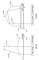
- FIG. 2A illustrates a first emitter 210A of infrared radiation positioned under the first proximity detector lens 104A with a first IR sensor 214A.
- FIG. 2B illustrates a second emitter 210B of infrared radiation positioned under the second proximity detector lens 104B with a second IR sensor 214B.
- a first beam 212A-1 of IR radiation is illustrated passing through a center point of the first amount of matter 106A.
- a second beam 212A-2 of IR radiation is illustrated passing through an off-center point of the first amount of matter 106A.
- the second beam 212A-2 passes through the boundary between the first amount of matter 106A and air, the second beam 212A-2 is refracted such that the second beam 212A-2, which is parallel to the first beam 212A-1 within the first amount of matter 106A, adopts a path toward the first beam 212A-1.
- the first beam 212A-1 and the second beam 212A-2 may reflect from a proximate object and take a return path through the first amount of matter 106A, the first proximity detector lens 104A and the IR transmitting ink layer 109 to be received by the first IR sensor 214A. Based on information, received from the first emitter 210A, the first IR sensor 214A may assess how proximate the object is to the associated smart phone.
- a first beam 212B-1 of IR radiation is illustrated passing through a center point of the second amount of matter 106B.
- a second beam 212B-2 of IR radiation is illustrated passing through an off-center point of the second amount of matter 106B.
- the second beam 212B-2 arrives at the boundary between the second amount of matter 106B and air, the second beam 212B-2 is reflected such that the second beam 212B-2, which is initially parallel to the first beam 212B-1 within the second amount of matter 106B, adopts a path toward the first beam 212A-1 within the second amount of matter 106B.
- the second beam 212B-2 arrives at another boundary between the second amount of matter 106B and air, the second beam 212B-2 is reflected such that the second beam 212B-2 adopts a path back toward the second proximity detector lens 104B.
- the first beam 212B-1 may reflect from a proximate object and take a return path through the second amount of matter 106B, the anti-fingerprint layer 108, the second proximity detector lens 104B and the IR transmitting ink layer 109 to be received by the second IR sensor 214B.
- the second beam 212B-2 may reflect, as illustrated, back to the second IR sensor 214B without having reached the object.
- the second IR sensor 214B may assess how proximate the object is to the associated smart phone. Given that the reflection of the first beam 212B-1 is inconsistent with the reflection of the second beam 212B-2, the second IR sensor 214B may not be able to form an accurate assessment regarding how proximate the object is to the associated smart phone.
- An increase in reflected IR beams may be measured when the second proximity detector lens 104B (with the anti-fingerprint layer 108) is compared to the first proximity detector lens 104A in the presence (on the lens 104A or on the anti-fingerprint layer 108) of material, such as water, sweat or oil.
- the increase in reflected IR beams may manifest as a reduced efficacy of proximity detection, as assessed by the second IR sensor 214B.
- the first proximity detector lens 104A and the second proximity detector lens 104B may be considered to have a refractive index of around 1.52. Air, of course, may be considered to have a refractive index of 1.00.
- the IR transmitting ink layer 109 may be considered to have a refractive index of around 1.45. Face oil may be considered to have a refractive index of around 1.40.
- an adapted system featuring a further layer on the underside of a proximity detector lens.
- the further layer has appropriately selected refractive index and transparency, proximity detection, as assessed by an IR sensor in the adapted system, may be improved over a system lacking the further layer.
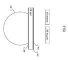
- FIG. 3 illustrates an adapted proximity detection system.
- the adapted system includes, in common with the system of FIG. 2B , an IR emitter and an IR sensor.
- FIG. 3 illustrates a third emitter 310 of infrared radiation positioned, with a third IR sensor 314, under a third proximity detector lens 304.
- the third proximity detector lens 304 has an anti-fingerprint coating 308 on one side and an IR transmitting ink layer 309 on the other side.
- a third amount of matter 306 is illustrated on the anti-fingerprint coating 308.
- the adapted system includes, distinct from the system of FIG. 2B , a proximity detection improvement layer 316 on the IR transmitting ink layer 309.
- a "high" refractive index may be defined as being a refractive index that is greater than the refractive index of the IR transmitting ink layer 309.
- a "high" transparency may be defined as being a transparency that is in the range from 80% to 99% inclusive.
- Example materials considered to be suitable for the proximity detection improvement layer 316 include titanium dioxide (TiO 2 ), zirconium dioxide (ZrO 2 ), tantalum pentoxide (Ta 2 O 5 ), zinc oxide (ZnO), silicon monoxide (SiO) and phenyl silicone (phenyl type SiO).
- the refractive index of a given material is different for different wavelengths of radiation.
- the wavelength range of interest extends roughly from 850nm to 1000nm.
- the refractive index of the suggested materials are as follows: Material Refractive index at 850nm titanium dioxide (TiO 2 ), 2.51 zirconium dioxide (ZrO 2 ) 2.17 tantalum pentoxide (Ta 2 O 5 ) 1.78 zinc oxide (ZnO) 1.95 silicon monoxide (SiO) 1.40 phenyl silicone (phenyl type SiO) 1.51
- the proximity detection improvement layer 316 may be added to the IR transmitting ink layer 309 by a printing process such that manufacturing of the smart phone screen of which the proximity detector lens 304 forms a part may remain straightforward and relatively low cost. Details of the printing process are expected to be known to a person of ordinary skill in the art of working with these materials. Further conveniently, it may be shown that the addition of the proximity detection improvement layer 316 has little impact on the thickness of the smart phone screen of which the proximity detector lens 304 forms a part.
- a method of manufacturing the mobile communication device display screen may begin with obtaining material suitable for a mobile communication device display screen.
- the suitable material may be glass having a hydrophobic layer on a first side. Such glass is typically available from Corning Incorporated of Corning, NY and from Asahi Glass Company of Tokyo, Japan.
- the method may include applying the IR transmitting ink layer 309 to the proximity detector lens 304.
- the method may also include printing the proximity detection improvement layer 316 on the IR transmitting ink layer 309.
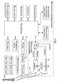
- FIG. 4 illustrates a mobile communication device 400 as an example of a device that may include the proximity detection system of FIG. 3 .
- the mobile communication device 400 includes a housing, an input device (e.g., a keyboard 424 having a plurality of keys) and an output device (e.g., a display 426), which may comprise a full graphic, or full color, Liquid Crystal Display (LCD).
- the display 426 may comprise a touchscreen display screen.
- the keyboard 424 may comprise a virtual keyboard.
- Other types of output devices may additionally, or alternatively, be utilized.
- a processing device (a microprocessor 428) is shown schematically in FIG. 4 as coupled between the keyboard 424 and the display 426.
- the microprocessor 428 controls the operation of the display 426, as well as the overall operation of the mobile communication device 400, in part, responsive to actuation of the keys on the keyboard 424 by a user.
- FIGS. 2A and 2B illustrate beams 212A-1, 212A-2, 212B-1, 212B-2 (collectively or individually 212) of IR radiation passing through the IR transmitting ink layer 109, the proximity detector lens 104, the amount of matter 106 and, in the case illustrated in FIG. 2B , the anti-fingerprint layer 108.
- all four of the illustrated beams 212 of IR radiation arrive at the IR transmitting ink layer 109 normal to the plane defined by the proximity detector lens 104. Accordingly, there is no refraction of the beams 212 illustrates in FIGS. 2A and 2B .
- the first emitter 210A, the second emitter 210B and the third IR emitter 310 emit IR radiation in a multitude of directions, with the result being that few, if any, of the beams of IR radiation that reach the plane defined by the proximity detector lens 104 are normal to that plane.
- n air refractive index 1.00
- the beam is refracted toward an axis normal to the plane defined by the proximity detector lens 104.
- an incident beam is refracted further toward an axis normal to the plane defined by the proximity detector lens 104.
- ⁇ air 30 degrees
- the resultant ⁇ pdi 14.86 degrees.
- an incident beam is refracted away from the axis normal to the plane defined by the proximity detector lens 104.
- the presence of the proximity detection improvement layer 316 leads to an increase in the IR radiation that is emitted from the third amount of matter 306, expressed, say, as a percentage of the IR radiation that is emitted from the emitter 310.
- the third amount of matter 306 compared to the IR radiation emitted from the second amount of matter 106B for the same initial conditions, it follows that comparatively more IR radiation will be returned to the third IR sensor 314 than would be returned to the second IR sensor 214B. With more IR radiation returned, it is anticipated that proximity detection would be improved.
- the signal to noise ratio of the radiation received by the third IR sensor 314 is higher than the signal to noise ratio of the radiation received by the second IR sensor 214B under identical conditions.
- FIG. 4 Elements of the proximity detection system of FIG. 3 , including the third IR emitter 310 and the third IR sensor 314, are illustrated in FIG. 4 , with the third IR sensor 314 in communication with the microprocessor 428 .
- the housing may be elongated vertically, or may take on other sizes and shapes (including clamshell housing structures).
- the keyboard 424 may include a mode selection key, or other hardware or software, for switching between alphabetic entry and numeric entry.
- the mobile communication device 400 may include a communications subsystem 402, a short-range communications subsystem 404, the keyboard 424 and the display 426.
- the mobile communication device 400 may further include other input/output devices, such as a set of auxiliary I/O devices 406, a serial port 408, a speaker 411 and a microphone 412.
- the mobile communication device 400 may further include memory devices including a flash memory 416 and a Random Access Memory (RAM) 418 and various other device subsystems 420.
- the mobile communication device 400 may comprise a two-way radio frequency (RF) communication device having voice and data communication capabilities.
- the mobile communication device 400 may have the capability to communicate with other computer systems via the Internet.
- RF radio frequency
- Operating system software executed by the microprocessor 428 may be stored in a computer readable medium, such as the flash memory 416, but may be stored in other types of memory devices, such as a read only memory (ROM) or similar storage element.
- system software, specific device applications, or parts thereof may be temporarily loaded into a volatile store, such as the RAM 418.
- Communication signals received by the mobile device may also be stored to the RAM 418.
- the microprocessor 428 in addition to its operating system functions, enables execution of software applications on the mobile communication device 400.
- a predetermined set of software applications that control basic device operations such as a voice communications module 430A and a data communications module 430B, may be installed on the mobile communication device 400 during manufacture.
- additional software modules illustrated as an other software module 430N, which may comprise, for instance, a personal information manager (PIM) application, may be installed during manufacture.
- the PIM application may be capable of organizing and managing data items, such as e-mail messages, calendar events, voice mail messages, appointments and task items.
- the PIM application may also be capable of sending and receiving data items via a wireless carrier network 470 represented by a radio tower.
- the data items managed by the PIM application may be seamlessly integrated, synchronized and updated via the wireless carrier network 470 with the device user's corresponding data items stored or associated with a host computer system.
- the communication subsystem 402 includes a receiver 450, a transmitter 452 and one or more antennas, illustrated as a receive antenna 454 and a transmit antenna 456.
- the communication subsystem 402 also includes a processing module, such as a digital signal processor (DSP) 458, and local oscillators (LOs) 460.
- DSP digital signal processor
- LOs local oscillators
- the specific design and implementation of the communication subsystem 402 is dependent upon the communication network in which the mobile communication device 400 is intended to operate.
- the communication subsystem 402 of the mobile communication device 400 may be designed to operate with mobile data communication networks and voice communication networks, such as, but not limited to, Long Term Evolution (LTE). Other types of data and voice networks, both separate and integrated, may also be utilized with the mobile communication device 400.
- LTE Long Term Evolution
- the mobile communication device 400 may send and receive communication signals over the wireless carrier network 470.
- Signals received from the wireless carrier network 470 by the receive antenna 454 are routed to the receiver 450, which provides for signal amplification, frequency down conversion, filtering, channel selection, etc., and may also provide analog to digital conversion. Analog-to-digital conversion of the received signal allows the DSP 458 to perform more complex communication functions, such as demodulation and decoding.
- signals to be transmitted to the wireless carrier network 470 are processed (e.g., modulated and encoded) by the DSP 458 and are then provided to the transmitter 452 for digital to analog conversion, frequency up conversion, filtering, amplification and transmission to the wireless carrier network 470 (or networks) via the transmit antenna 456.
- the DSP 458 provides for control of the receiver 450 and the transmitter 452. For example, gains applied to communication signals in the receiver 450 and the transmitter 452 may be adaptively controlled through automatic gain control algorithms implemented in the DSP 458.
- a received signal such as a text message or web page download
- the communication subsystem 402 is input to the microprocessor 428.
- the received signal is then further processed by the microprocessor 428 for output to the display 426, or alternatively to some auxiliary I/O devices 406.
- a device user may also compose data items, such as e-mail messages, using the keyboard 424 and/or some other auxiliary I/O device 406, such as a touchpad, a rocker switch, a thumb-wheel, a trackball, a touchscreen, or some other type of input device.
- the composed data items may then be transmitted over the wireless carrier network 470 via the communication subsystem 402.
- a voice communication mode In a voice communication mode, overall operation of the device is substantially similar to the data communication mode, except that received signals are output to the speaker 411, and signals for transmission are generated by a microphone 412.
- Alternative voice or audio I/O subsystems such as a voice message recording subsystem, may also be implemented on the mobile communication device 400.
- the display 426 may also be utilized in voice communication mode, for example, to display the identity of a calling party, the duration of a voice call, or other voice call related information.
- the short-range communications subsystem 404 enables communication between the mobile communication device 400 and other proximate systems or devices, which need not necessarily be similar devices.
- the short-range communications subsystem may include an infrared device and associated circuits and components, or a BluetoothTM communication module to provide for communication with similarly-enabled systems and devices, or a near field communication module, etc.
Landscapes
- Engineering & Computer Science (AREA)
- Physics & Mathematics (AREA)
- Computer Networks & Wireless Communication (AREA)
- General Physics & Mathematics (AREA)
- Radar, Positioning & Navigation (AREA)
- Remote Sensing (AREA)
- Electromagnetism (AREA)
- Telephone Set Structure (AREA)
- Telephone Function (AREA)
Abstract
Description
- The present application relates generally to proximity detection in mobile communication devices and, more specifically, to a mobile communication device with a lens overlaying a proximity detector and where the lens has a layer having qualities that lead to improved proximity detection.
- It is common for a modern smart phone to include a proximity sensor. In particular, a proximity sensor is especially of use in smart phones that have a touchscreen. Beneficially, a smart phone may be configured to ignore receipt of input from the touchscreen under certain circumstances. For example, such circumstances may include receipt of input from a proximity sensor that indicates that a user is holding the smart phone against the user's head while, for example, involved in a telephone call. Responsive to the user removing the smart phone from against the user's head, say, at the end of the telephone call or to review data on the smart phone in the midst of the telephone call, input from the proximity sensor may allow the smart phone to resume considering receipt of input from the touch screen.
- Accordingly there is provided a lens, detection system and mobile device as detailed in the claims that follow. Advantageous features are provided in the dependent claims. An independent method is also provided.
- Reference will now be made, by way of example, to the accompanying drawings which show example implementations; and in which:
-
FIG. 1A illustrates a first proximity detector lens with a first amount of matter resting thereon; -
FIG. 1B illustrates a second proximity detector lens with a second amount of matter resting thereon; -
FIG. 2A illustrates the first proximity detector lens ofFIG. 1A with a first emitter of infrared radiation positioned under the first proximity detector lens with a first IR sensor; -
FIG. 2B illustrates the second proximity detector lens ofFIG. 1B with a second emitter of infrared radiation positioned under the second proximity detector lens with a second IR sensor; -
FIG. 3 illustrates an adapted proximity detection system including, in accordance with an embodiment of the present application, an IR emitter and an IR sensor positioned under a third proximity detector lens; and -
FIG. 4 illustrates a mobile communication device as an example of a device that may include the adapted proximity detection system ofFIG. 3 . - Frequently, as a result of the user holding the smart phone against the user's head, there is a transfer of matter from the user's head to the touchscreen of the smart phone. The matter may be, for just three examples, water, sweat and/or oil. In cases for which the smart phone touchscreen is uncoated glass, there is typically minimal adverse effect caused by the presence of the matter. However, modern smart phones often include an anti-fingerprint coating, on the outer surface of the glass screen. The anti-fingerprint coating is specifically designed to reduce the appearance of fingerprints and smudges. However, the properties of the anti-fingerprint coating may have unintended consequences for proximity sensing. That is, when matter is deposited on the anti-fingerprint coated screen of the smart phone, especially in an area of the screen overlaying the proximity sensor, the matter may hamper correct operation of the proximity sensor, which, in turn, may hamper expected operation of the smart phone. For example, if the matter on the anti-fingerprint coated screen of the smart phone prevents the proximity sensor from determining that the smart phone has been taken away from the user's head, the smart phone may not appropriately resume considering receipt of input from the touch screen.
- The area of the screen overlaying the proximity sensor may be called a lens.
- Although the screen of the typical smart phone is referenced above as glass, a person of ordinary skill in the art of smart phone displays will understand that the material for the screen is often a modern polymer.
- It is proposed herein to add a new layer to the inner surface of the proximity detector lens of, for example, a smart phone. The new layer, with beneficial qualities such as high transparency and high refractive index, may be seen to improve proximity sensor performance in the presence of matter on a smart phone touchscreen with an anti-fingerprint coating.
- According to an aspect of the present disclosure, there is provided a proximity detector lens. The proximity detector lens includes a hydrophobic layer on a first side of the lens, an infrared transmitting ink layer on a second side of the lens, the infrared transmitting ink layer having an infrared transmitting ink layer refractive index and a proximity detection improvement layer on the infrared transmitting ink layer, the proximity detection improvement layer having a proximity detection improvement layer refractive index that is greater than the infrared transmitting ink layer refractive index.
- According to a further aspect of the present disclosure, there is provided a proximity detection system. The system includes an emitter of infrared radiation, a sensor of infrared radiation and a proximity detector lens overlaying the emitter. The lens includes a hydrophobic layer on a first side of the lens, an infrared transmitting ink layer on a second side of the lens, the second side of the lens facing the emitter, the infrared transmitting ink layer having an infrared transmitting ink layer refractive index and a proximity detection improvement layer on the infrared transmitting ink layer, the proximity detection improvement layer having a proximity detection improvement layer refractive index that is greater than the infrared transmitting ink layer refractive index.
- According to an even further aspect of the present disclosure, there is provided a mobile communication device. The device includes an emitter of infrared radiation, a sensor of infrared radiation and a display screen. A portion of the display screen is designated as a proximity detector lens overlaying the emitter. The lens includes a hydrophobic layer on a first side of the lens, an infrared transmitting ink layer on a second side of the lens, the second side of the lens facing the emitter, the infrared transmitting ink layer having an infrared transmitting ink layer refractive index and a proximity detection improvement layer on the infrared transmitting ink layer, the proximity detection improvement layer having a proximity detection improvement layer refractive index that is greater than the infrared transmitting ink layer refractive index
- Other aspects and features of the present disclosure will become apparent to those of ordinary skill in the art upon review of the following description of specific implementations of the disclosure in conjunction with the accompanying figures.
- It is known that there are a variety of technology options for proximity detection. Inductive sensors and capacitive sensors may be grouped together as each using electrical technology. Infrared sensors, ambient light sensors and LASER sensors may be grouped together as each using optical technology. Other options available include sensors employing magnetic technology and sensors employing SONAR technology.
- When infrared (IR) radiation is used for proximity detection, an emitter is controlled to emit IR radiation and a sensor is used to determine an extent to which the emitted IR radiation has been reflected back to the sensor. In this proximity detection scheme, an extent of reflected IR radiation that exceeds a threshold may be interpreted as indicative of the smart phone being in close proximity to something.
-
FIG. 1A illustrates a firstproximity detector lens 104A. A first amount ofmatter 106A rests on the firstproximity detector lens 104A. -
FIG. 1B illustrates a secondproximity detector lens 104B. InFIG. 1B , the secondproximity detector lens 104B includes ananti-fingerprint layer 108. A second amount ofmatter 106B rests on theanti-fingerprint layer 108. - Both the first
proximity detector lens 104A and the secondproximity detector lens 104B may be coated, on the underside, with IR transmittingink layer 109. The IR transmittingink layer 109 can be selected for color and for which wavelengths the IR transmittingink layer 109 transmits, to fulfill various needs on transparent sheet material like smart phone touch screens. Example IR transmitting inks suitable for the IRtransmitting ink layer 109 include inks in the 1400N series from Seiko of Tokyo, Japan and inks in the GLS-HF series from Teikoku of Tokyo, Japan. - The difference between the shape that the
matter 106A takes inFIG. 1A and the shape that thematter 106B takes inFIG. 1B should be evident and can be explained as being a result of the firstproximity detector lens 104A (FIG. 1A ) being hydrophilic and theanti-fingerprint layer 108 being hydrophobic. As a consequence of the hydrophobic quality of theanti-fingerprint layer 108, the second amount ofmatter 106B displays a greater surface tension that the first amount ofmatter 106A. -
FIG. 2A illustrates afirst emitter 210A of infrared radiation positioned under the firstproximity detector lens 104A with afirst IR sensor 214A.FIG. 2B illustrates asecond emitter 210B of infrared radiation positioned under the secondproximity detector lens 104B with asecond IR sensor 214B. - In
FIG. 2A , afirst beam 212A-1 of IR radiation is illustrated passing through a center point of the first amount ofmatter 106A. Additionally, asecond beam 212A-2 of IR radiation is illustrated passing through an off-center point of the first amount ofmatter 106A. As thesecond beam 212A-2 passes through the boundary between the first amount ofmatter 106A and air, thesecond beam 212A-2 is refracted such that thesecond beam 212A-2, which is parallel to thefirst beam 212A-1 within the first amount ofmatter 106A, adopts a path toward thefirst beam 212A-1. - In operation, the
first beam 212A-1 and thesecond beam 212A-2 may reflect from a proximate object and take a return path through the first amount ofmatter 106A, the firstproximity detector lens 104A and the IRtransmitting ink layer 109 to be received by thefirst IR sensor 214A. Based on information, received from thefirst emitter 210A, thefirst IR sensor 214A may assess how proximate the object is to the associated smart phone. - In
FIG. 2B , afirst beam 212B-1 of IR radiation is illustrated passing through a center point of the second amount ofmatter 106B. Additionally, asecond beam 212B-2 of IR radiation is illustrated passing through an off-center point of the second amount ofmatter 106B. As thesecond beam 212B-2 arrives at the boundary between the second amount ofmatter 106B and air, thesecond beam 212B-2 is reflected such that thesecond beam 212B-2, which is initially parallel to thefirst beam 212B-1 within the second amount ofmatter 106B, adopts a path toward thefirst beam 212A-1 within the second amount ofmatter 106B. As thesecond beam 212B-2 arrives at another boundary between the second amount ofmatter 106B and air, thesecond beam 212B-2 is reflected such that thesecond beam 212B-2 adopts a path back toward the secondproximity detector lens 104B. - In operation, the
first beam 212B-1 may reflect from a proximate object and take a return path through the second amount ofmatter 106B, theanti-fingerprint layer 108, the secondproximity detector lens 104B and the IRtransmitting ink layer 109 to be received by thesecond IR sensor 214B. Also, thesecond beam 212B-2 may reflect, as illustrated, back to thesecond IR sensor 214B without having reached the object. Based on information, received from thesecond emitter 210B, thesecond IR sensor 214B may assess how proximate the object is to the associated smart phone. Given that the reflection of thefirst beam 212B-1 is inconsistent with the reflection of thesecond beam 212B-2, thesecond IR sensor 214B may not be able to form an accurate assessment regarding how proximate the object is to the associated smart phone. - An increase in reflected IR beams may be measured when the second
proximity detector lens 104B (with the anti-fingerprint layer 108) is compared to the firstproximity detector lens 104A in the presence (on thelens 104A or on the anti-fingerprint layer 108) of material, such as water, sweat or oil. - The increase in reflected IR beams may manifest as a reduced efficacy of proximity detection, as assessed by the
second IR sensor 214B. - The first
proximity detector lens 104A and the secondproximity detector lens 104B may be considered to have a refractive index of around 1.52. Air, of course, may be considered to have a refractive index of 1.00. The IRtransmitting ink layer 109 may be considered to have a refractive index of around 1.45. Face oil may be considered to have a refractive index of around 1.40. - In overview, it is proposed herein to provide an adapted system featuring a further layer on the underside of a proximity detector lens. When the further layer has appropriately selected refractive index and transparency, proximity detection, as assessed by an IR sensor in the adapted system, may be improved over a system lacking the further layer.
-
FIG. 3 illustrates an adapted proximity detection system. The adapted system includes, in common with the system ofFIG. 2B , an IR emitter and an IR sensor. In particular,FIG. 3 illustrates athird emitter 310 of infrared radiation positioned, with athird IR sensor 314, under a thirdproximity detector lens 304. The thirdproximity detector lens 304 has ananti-fingerprint coating 308 on one side and an IRtransmitting ink layer 309 on the other side. A third amount ofmatter 306 is illustrated on theanti-fingerprint coating 308. The adapted system includes, distinct from the system ofFIG. 2B , a proximitydetection improvement layer 316 on the IRtransmitting ink layer 309. - As discussed briefly hereinbefore, it is proposed herein to select the proximity
detection improvement layer 316 to have high transparency and high refractive index. To clarify, a "high" refractive index may be defined as being a refractive index that is greater than the refractive index of the IRtransmitting ink layer 309. To further clarify, a "high" transparency may be defined as being a transparency that is in the range from 80% to 99% inclusive. - Example materials considered to be suitable for the proximity
detection improvement layer 316 include titanium dioxide (TiO2), zirconium dioxide (ZrO2), tantalum pentoxide (Ta2O5), zinc oxide (ZnO), silicon monoxide (SiO) and phenyl silicone (phenyl type SiO). - As will be understood, the refractive index of a given material is different for different wavelengths of radiation. For proximity detection systems, the wavelength range of interest extends roughly from 850nm to 1000nm. At 850nm, the refractive index of the suggested materials are as follows:
Material Refractive index at 850nm titanium dioxide (TiO2), 2.51 zirconium dioxide (ZrO2) 2.17 tantalum pentoxide (Ta2O5) 1.78 zinc oxide (ZnO) 1.95 silicon monoxide (SiO) 1.40 phenyl silicone (phenyl type SiO) 1.51 - Off-the-shelf components with high Refractive Index include LaSF glass from Schott North America, Inc. of Duryea, PA (n in between 1.9 and 2.1), sheets of polythiourethane (n = 1.61), sheets of polycarbonate (n = 1.59) or sheets of Acrylic film (n = 1.60 to 1.80) and Optical Adhesive (n around 1.58 - 1.65).
- Conveniently, the proximity
detection improvement layer 316 may be added to the IRtransmitting ink layer 309 by a printing process such that manufacturing of the smart phone screen of which theproximity detector lens 304 forms a part may remain straightforward and relatively low cost. Details of the printing process are expected to be known to a person of ordinary skill in the art of working with these materials. Further conveniently, it may be shown that the addition of the proximitydetection improvement layer 316 has little impact on the thickness of the smart phone screen of which theproximity detector lens 304 forms a part. - A method of manufacturing the mobile communication device display screen, a portion of which is illustrated in
FIG. 3 , may begin with obtaining material suitable for a mobile communication device display screen. The suitable material may be glass having a hydrophobic layer on a first side. Such glass is typically available from Corning Incorporated of Corning, NY and from Asahi Glass Company of Tokyo, Japan. Where a portion of the display screen is designated as theproximity detector lens 304 overlaying thethird IR emitter 310, the method may include applying the IRtransmitting ink layer 309 to theproximity detector lens 304. The method may also include printing the proximitydetection improvement layer 316 on the IRtransmitting ink layer 309. - While, to this point, the proximity
detection improvement layer 316 has been presented as particularly useful in the context of aproximity detector lens 304, it is also worth noting that the proximitydetection improvement layer 316 may find uses on the underside of an optical touchpad navigating device (not shown) and, indeed, in any application similar to the proximity detector example, where something is determined through the transmission of IR through a medium and measurement of the reflections.FIG. 4 illustrates amobile communication device 400 as an example of a device that may include the proximity detection system ofFIG. 3 . Themobile communication device 400 includes a housing, an input device (e.g., akeyboard 424 having a plurality of keys) and an output device (e.g., a display 426), which may comprise a full graphic, or full color, Liquid Crystal Display (LCD). In some embodiments, thedisplay 426 may comprise a touchscreen display screen. In such embodiments, thekeyboard 424 may comprise a virtual keyboard. Other types of output devices may additionally, or alternatively, be utilized. A processing device (a microprocessor 428) is shown schematically inFIG. 4 as coupled between thekeyboard 424 and thedisplay 426. Themicroprocessor 428 controls the operation of thedisplay 426, as well as the overall operation of themobile communication device 400, in part, responsive to actuation of the keys on thekeyboard 424 by a user. -
FIGS. 2A and 2B illustratebeams 212A-1, 212A-2, 212B-1, 212B-2 (collectively or individually 212) of IR radiation passing through the IRtransmitting ink layer 109, the proximity detector lens 104, the amount of matter 106 and, in the case illustrated inFIG. 2B , theanti-fingerprint layer 108. Notably, all four of the illustrated beams 212 of IR radiation arrive at the IRtransmitting ink layer 109 normal to the plane defined by the proximity detector lens 104. Accordingly, there is no refraction of the beams 212 illustrates inFIGS. 2A and 2B . In reality, however, thefirst emitter 210A, thesecond emitter 210B and thethird IR emitter 310 emit IR radiation in a multitude of directions, with the result being that few, if any, of the beams of IR radiation that reach the plane defined by the proximity detector lens 104 are normal to that plane. - At the boundary between air (with refractive index nair = 1.00) and the IR transmitting ink layer 109 (with, e.g., refractive index nir = 1.45), a beam of IR radiation approaching at an angle θair is expected to be refracted in a manner in accordance with the relationship nir x sin(θir) = nair x sin(θair). According to this relationship, when the initial refractive index (θair, in this case) is less than the subsequent refractive index (θir, in this case), the beam is refracted toward an axis normal to the plane defined by the proximity detector lens 104. For example, when θair = 30 degrees, the resultant θir = 20.17 degrees. It follows that the beam incident at the border between the IR
transmitting ink layer 109 and the proximity detector lens 104 may be defined, in part, by the angle θir = 20.17. - In the embodiment presented in
FIG. 3 , at the boundary between air and the proximity detection improvement layer 316 (with, e.g., refractive index npdi = 1.95), an incident beam is refracted further toward an axis normal to the plane defined by the proximity detector lens 104. For example, when θair = 30 degrees, the resultant θpdi = 14.86 degrees. At the boundary between the proximitydetection improvement layer 316 and the IRtransmitting ink layer 309, an incident beam is refracted away from the axis normal to the plane defined by the proximity detector lens 104. Notably, it follows that the beam incident at the border between the IRtransmitting ink layer 109 and the proximity detector lens 104 may be defined, in part, by the angle θir = 20.17, which is the same as in the case wherein the proximitydetection improvement layer 316 is absent. - It is worth noting that the IR
transmitting ink layer 309 is not a transparent layer. Indeed, it is anticipated that the IRtransmitting ink layer 309 will scatter the incident beams. That is, not all of the 30-degree-incident beams on the border between air and the IRtransmitting ink layer 309 on the proximity detector lens 104 will continue on through the IRtransmitting ink layer 109/309 and approach the border between the IRtransmitting ink layer 109/309 and the proximity detector lens 104 at the angle θir = 20.17, as would be predicted if the IRtransmitting ink layer 109/309 was transparent. For some beams, the angle will be higher; for other beams the angle will be lower. It can be shown, through simulation, that the presence of the proximitydetection improvement layer 316 leads to an increase in the IR radiation that is emitted from the third amount ofmatter 306, expressed, say, as a percentage of the IR radiation that is emitted from theemitter 310. As a consequence of more IR radiation being emitted from the third amount ofmatter 306, compared to the IR radiation emitted from the second amount ofmatter 106B for the same initial conditions, it follows that comparatively more IR radiation will be returned to thethird IR sensor 314 than would be returned to thesecond IR sensor 214B. With more IR radiation returned, it is anticipated that proximity detection would be improved. - As a general observation, it may be considered that, due to the presence of the proximity
detection improvement layer 316, the signal to noise ratio of the radiation received by thethird IR sensor 314 is higher than the signal to noise ratio of the radiation received by thesecond IR sensor 214B under identical conditions. - Elements of the proximity detection system of
FIG. 3 , including thethird IR emitter 310 and thethird IR sensor 314, are illustrated inFIG. 4 , with thethird IR sensor 314 in communication with themicroprocessor 428 . - The housing may be elongated vertically, or may take on other sizes and shapes (including clamshell housing structures). In the case in which the
keyboard 424 includes keys that are associated with at least one alphabetic character and at least one numeric character, thekeyboard 424 may include a mode selection key, or other hardware or software, for switching between alphabetic entry and numeric entry. - In addition to the
microprocessor 428, other parts of themobile communication device 400 are shown schematically inFIG. 4 . These may include acommunications subsystem 402, a short-range communications subsystem 404, thekeyboard 424 and thedisplay 426. Themobile communication device 400 may further include other input/output devices, such as a set of auxiliary I/O devices 406, aserial port 408, aspeaker 411 and amicrophone 412. Themobile communication device 400 may further include memory devices including aflash memory 416 and a Random Access Memory (RAM) 418 and variousother device subsystems 420. Themobile communication device 400 may comprise a two-way radio frequency (RF) communication device having voice and data communication capabilities. In addition, themobile communication device 400 may have the capability to communicate with other computer systems via the Internet. - Operating system software executed by the
microprocessor 428 may be stored in a computer readable medium, such as theflash memory 416, but may be stored in other types of memory devices, such as a read only memory (ROM) or similar storage element. In addition, system software, specific device applications, or parts thereof, may be temporarily loaded into a volatile store, such as theRAM 418. Communication signals received by the mobile device may also be stored to theRAM 418. - The
microprocessor 428, in addition to its operating system functions, enables execution of software applications on themobile communication device 400. A predetermined set of software applications that control basic device operations, such as avoice communications module 430A and adata communications module 430B, may be installed on themobile communication device 400 during manufacture. As well, additional software modules, illustrated as another software module 430N, which may comprise, for instance, a personal information manager (PIM) application, may be installed during manufacture. The PIM application may be capable of organizing and managing data items, such as e-mail messages, calendar events, voice mail messages, appointments and task items. The PIM application may also be capable of sending and receiving data items via awireless carrier network 470 represented by a radio tower. The data items managed by the PIM application may be seamlessly integrated, synchronized and updated via thewireless carrier network 470 with the device user's corresponding data items stored or associated with a host computer system. - Communication functions, including data and voice communications, are performed through the
communication subsystem 402 and, possibly, through the short-range communications subsystem 404. Thecommunication subsystem 402 includes areceiver 450, atransmitter 452 and one or more antennas, illustrated as a receiveantenna 454 and a transmitantenna 456. In addition, thecommunication subsystem 402 also includes a processing module, such as a digital signal processor (DSP) 458, and local oscillators (LOs) 460. The specific design and implementation of thecommunication subsystem 402 is dependent upon the communication network in which themobile communication device 400 is intended to operate. For example, thecommunication subsystem 402 of themobile communication device 400 may be designed to operate with mobile data communication networks and voice communication networks, such as, but not limited to, Long Term Evolution (LTE). Other types of data and voice networks, both separate and integrated, may also be utilized with themobile communication device 400. - The
mobile communication device 400 may send and receive communication signals over thewireless carrier network 470. Signals received from thewireless carrier network 470 by the receiveantenna 454 are routed to thereceiver 450, which provides for signal amplification, frequency down conversion, filtering, channel selection, etc., and may also provide analog to digital conversion. Analog-to-digital conversion of the received signal allows theDSP 458 to perform more complex communication functions, such as demodulation and decoding. In a similar manner, signals to be transmitted to thewireless carrier network 470 are processed (e.g., modulated and encoded) by theDSP 458 and are then provided to thetransmitter 452 for digital to analog conversion, frequency up conversion, filtering, amplification and transmission to the wireless carrier network 470 (or networks) via the transmitantenna 456. - In addition to processing communication signals, the
DSP 458 provides for control of thereceiver 450 and thetransmitter 452. For example, gains applied to communication signals in thereceiver 450 and thetransmitter 452 may be adaptively controlled through automatic gain control algorithms implemented in theDSP 458. - In a data communication mode, a received signal, such as a text message or web page download, is processed by the
communication subsystem 402 and is input to themicroprocessor 428. The received signal is then further processed by themicroprocessor 428 for output to thedisplay 426, or alternatively to some auxiliary I/O devices 406. A device user may also compose data items, such as e-mail messages, using thekeyboard 424 and/or some other auxiliary I/O device 406, such as a touchpad, a rocker switch, a thumb-wheel, a trackball, a touchscreen, or some other type of input device. The composed data items may then be transmitted over thewireless carrier network 470 via thecommunication subsystem 402. - In a voice communication mode, overall operation of the device is substantially similar to the data communication mode, except that received signals are output to the
speaker 411, and signals for transmission are generated by amicrophone 412. Alternative voice or audio I/O subsystems, such as a voice message recording subsystem, may also be implemented on themobile communication device 400. In addition, thedisplay 426 may also be utilized in voice communication mode, for example, to display the identity of a calling party, the duration of a voice call, or other voice call related information. - The short-range communications subsystem 404 enables communication between the
mobile communication device 400 and other proximate systems or devices, which need not necessarily be similar devices. For example, the short-range communications subsystem may include an infrared device and associated circuits and components, or a Bluetooth™ communication module to provide for communication with similarly-enabled systems and devices, or a near field communication module, etc. - The above-described implementations of the present application are intended to be examples only. Alterations, modifications and variations may be effected to the particular implementations by those skilled in the art without departing from the scope of the application, which is defined by the claims appended hereto.
Claims (7)
- A proximity detector lens comprising:a hydrophobic layer (308) on a first side of the lens (304);an infrared transmitting ink layer (309) on a second side of the lens, the infrared transmitting ink layer having an infrared transmitting ink layer refractive index; anda proximity detection improvement layer (316) on the infrared transmitting ink layer, the proximity detection improvement layer having a proximity detection improvement layer refractive index at a given wavelength that is greater than the infrared transmitting ink layer refractive index at the given wavelength.
- The proximity detector lens of claim 1 wherein the infrared transmitting ink layer refractive index is around 1.45 index at the given wavelength.
- The proximity detector lens of claim 2 wherein the proximity detection improvement layer comprises one of titanium dioxide, zirconium dioxide, tantalum pentoxide, zinc oxide, silicon monoxide and phenyl silicone.
- The proximity detector lens of any one of claims 1 to 3 wherein the given wavelength is in the range from 850nm to 1000nm.
- A proximity detection system comprising:an emitter (310) of infrared radiation;a sensor (314) of infrared radiation;a proximity detector lens (304) as claimed in any preceding claim, the lens overlaying the emitter and arranged such that the second side of the lens faces the emitter.
- A mobile communication device (400) comprising a proximity detection system as claimed in claim 5, the device comprising a display screen (426), a portion of the display screen designated as the proximity detector lens overlaying the emitter.
- A method of manufacturing a proximity detector lens (304) designed for overlaying an emitter of infrared radiation, the mobile communication device display screen having a hydrophobic layer on a first side, the method comprising:applying an infrared transmitting ink layer (309) on a second side of the lens portion of the display screen, the infrared transmitting ink layer having an infrared transmitting ink layer refractive index; andprinting a proximity detection improvement layer (316) on the infrared transmitting ink layer, the proximity detection improvement layer having a proximity detection improvement layer refractive index at a given wavelength that is greater than the infrared transmitting ink layer refractive index at the given wavelength.
Applications Claiming Priority (1)
| Application Number | Priority Date | Filing Date | Title |
|---|---|---|---|
| US14/312,863 US20150369906A1 (en) | 2014-06-24 | 2014-06-24 | Lens with proximity detection performance improvement layer |
Publications (1)
| Publication Number | Publication Date |
|---|---|
| EP2960676A1 true EP2960676A1 (en) | 2015-12-30 |
Family
ID=53491300
Family Applications (1)
| Application Number | Title | Priority Date | Filing Date |
|---|---|---|---|
| EP15173415.9A Withdrawn EP2960676A1 (en) | 2014-06-24 | 2015-06-23 | Lens with proximity detection performance improvement layer |
Country Status (2)
| Country | Link |
|---|---|
| US (1) | US20150369906A1 (en) |
| EP (1) | EP2960676A1 (en) |
Families Citing this family (2)
| Publication number | Priority date | Publication date | Assignee | Title |
|---|---|---|---|---|
| CN113523548B (en) * | 2021-07-26 | 2023-05-02 | 天津荣盛盟固利新能源科技有限公司 | Method for detecting dirt degree of laser welding protective lens |
| CN115469319B (en) * | 2022-09-14 | 2025-10-17 | 维沃移动通信有限公司 | Display device and electronic apparatus |
Citations (3)
| Publication number | Priority date | Publication date | Assignee | Title |
|---|---|---|---|---|
| US20120129579A1 (en) * | 2010-11-19 | 2012-05-24 | Apple Inc. | Proximity sensor arrangement in a mobile device |
| EP2595366A1 (en) * | 2011-11-18 | 2013-05-22 | Research In Motion Limited | Touch tracking optical input device |
| EP2728387A1 (en) * | 2012-10-31 | 2014-05-07 | ams AG | Proximity sensor module |
Family Cites Families (1)
| Publication number | Priority date | Publication date | Assignee | Title |
|---|---|---|---|---|
| US9465442B2 (en) * | 2013-02-05 | 2016-10-11 | Apple Inc. | Optical proximity sensor system having reduced sensitivity to distinct near-field optical effects |
-
2014
- 2014-06-24 US US14/312,863 patent/US20150369906A1/en not_active Abandoned
-
2015
- 2015-06-23 EP EP15173415.9A patent/EP2960676A1/en not_active Withdrawn
Patent Citations (3)
| Publication number | Priority date | Publication date | Assignee | Title |
|---|---|---|---|---|
| US20120129579A1 (en) * | 2010-11-19 | 2012-05-24 | Apple Inc. | Proximity sensor arrangement in a mobile device |
| EP2595366A1 (en) * | 2011-11-18 | 2013-05-22 | Research In Motion Limited | Touch tracking optical input device |
| EP2728387A1 (en) * | 2012-10-31 | 2014-05-07 | ams AG | Proximity sensor module |
Non-Patent Citations (1)
| Title |
|---|
| "Product Information Mylar - Optical Properties", 30 June 2003 (2003-06-30), XP055220880, Retrieved from the Internet <URL:http://usa.dupontteijinfilms.com/informationcenter/downloads/Optical_Properties.pdf> [retrieved on 20151014] * |
Also Published As
| Publication number | Publication date |
|---|---|
| US20150369906A1 (en) | 2015-12-24 |
Similar Documents
| Publication | Publication Date | Title |
|---|---|---|
| EP3809326B1 (en) | Display screen, and electronic device | |
| US10139532B2 (en) | Camera module and terminal | |
| KR102342609B1 (en) | Lcd display screen, electronic device, manufacturing method for lcd display screen | |
| US10503952B2 (en) | Fingerprint identification display device | |
| ES2977973T3 (en) | Method and apparatus of exposure | |
| CN108279408B (en) | Proximity sensor calibration method, device, mobile terminal and computer readable medium | |
| CN109300942B (en) | Display panel and display device having the same | |
| CN117590558B (en) | Optical transmission components, camera modules and electronic equipment | |
| CN109557697B (en) | A display adjustment method and terminal | |
| WO2012054517A2 (en) | System and method to manage visual voice mail messages | |
| US11720209B2 (en) | Pressure detection apparatus, screen assembly, and mobile terminal | |
| CN107463897B (en) | Fingerprint identification method and mobile terminal | |
| US20110261015A1 (en) | Optical touch display device | |
| US11004364B2 (en) | Supporting structure for flexible screen, flexible screen structure and terminal device | |
| EP2960676A1 (en) | Lens with proximity detection performance improvement layer | |
| WO2021097719A1 (en) | Under-screen fingerprint recognition device and system, light guide plate assembly and liquid crystal display screen | |
| WO2025195219A1 (en) | Display panel and electronic device | |
| CN112462463A (en) | Anti-reflective infrared cut filter coatings for electronic devices | |
| US20220308381A1 (en) | Display panel and display apparatus | |
| WO2026056608A1 (en) | Display module, display screen, electronic device, and display control method | |
| CN110149429B (en) | Terminal equipment | |
| EP4040223B1 (en) | Display panel and display device | |
| EP4040229B1 (en) | Liquid crystal display panel and liquid crystal display device | |
| US11010582B2 (en) | TFT panel type fingerprint recognition sensor | |
| JP2017505480A (en) | Optical film and digital pen system using the same |
Legal Events
| Date | Code | Title | Description |
|---|---|---|---|
| PUAI | Public reference made under article 153(3) epc to a published international application that has entered the european phase |
Free format text: ORIGINAL CODE: 0009012 |
|
| AK | Designated contracting states |
Kind code of ref document: A1 Designated state(s): AL AT BE BG CH CY CZ DE DK EE ES FI FR GB GR HR HU IE IS IT LI LT LU LV MC MK MT NL NO PL PT RO RS SE SI SK SM TR |
|
| AX | Request for extension of the european patent |
Extension state: BA ME |
|
| STAA | Information on the status of an ep patent application or granted ep patent |
Free format text: STATUS: THE APPLICATION HAS BEEN WITHDRAWN |
|
| 17P | Request for examination filed |
Effective date: 20160630 |
|
| RBV | Designated contracting states (corrected) |
Designated state(s): AL AT BE BG CH CY CZ DE DK EE ES FI FR GB GR HR HU IE IS IT LI LT LU LV MC MK MT NL NO PL PT RO RS SE SI SK SM TR |
|
| RIN1 | Information on inventor provided before grant (corrected) |
Inventor name: LEE, HSIN CHIN Inventor name: GAO, YU Inventor name: BROGA, ANTANAS MATTHEW |
|
| R17P | Request for examination filed (corrected) |
Effective date: 20160630 |
|
| 18W | Application withdrawn |
Effective date: 20160727 |