EP2958102A1 - Reduced off current switching transistor in an organic light-emitting diode display device - Google Patents
Reduced off current switching transistor in an organic light-emitting diode display device Download PDFInfo
- Publication number
- EP2958102A1 EP2958102A1 EP15172514.0A EP15172514A EP2958102A1 EP 2958102 A1 EP2958102 A1 EP 2958102A1 EP 15172514 A EP15172514 A EP 15172514A EP 2958102 A1 EP2958102 A1 EP 2958102A1
- Authority
- EP
- European Patent Office
- Prior art keywords
- gate
- layer
- interlayer dielectric
- display device
- insulating layer
- Prior art date
- Legal status (The legal status is an assumption and is not a legal conclusion. Google has not performed a legal analysis and makes no representation as to the accuracy of the status listed.)
- Ceased
Links
Images






Classifications
-
- G—PHYSICS
- G09—EDUCATION; CRYPTOGRAPHY; DISPLAY; ADVERTISING; SEALS
- G09G—ARRANGEMENTS OR CIRCUITS FOR CONTROL OF INDICATING DEVICES USING STATIC MEANS TO PRESENT VARIABLE INFORMATION
- G09G3/00—Control arrangements or circuits, of interest only in connection with visual indicators other than cathode-ray tubes
- G09G3/20—Control arrangements or circuits, of interest only in connection with visual indicators other than cathode-ray tubes for presentation of an assembly of a number of characters, e.g. a page, by composing the assembly by combination of individual elements arranged in a matrix no fixed position being assigned to or needed to be assigned to the individual characters or partial characters
- G09G3/22—Control arrangements or circuits, of interest only in connection with visual indicators other than cathode-ray tubes for presentation of an assembly of a number of characters, e.g. a page, by composing the assembly by combination of individual elements arranged in a matrix no fixed position being assigned to or needed to be assigned to the individual characters or partial characters using controlled light sources
- G09G3/30—Control arrangements or circuits, of interest only in connection with visual indicators other than cathode-ray tubes for presentation of an assembly of a number of characters, e.g. a page, by composing the assembly by combination of individual elements arranged in a matrix no fixed position being assigned to or needed to be assigned to the individual characters or partial characters using controlled light sources using electroluminescent panels
- G09G3/32—Control arrangements or circuits, of interest only in connection with visual indicators other than cathode-ray tubes for presentation of an assembly of a number of characters, e.g. a page, by composing the assembly by combination of individual elements arranged in a matrix no fixed position being assigned to or needed to be assigned to the individual characters or partial characters using controlled light sources using electroluminescent panels semiconductive, e.g. using light-emitting diodes [LED]
- G09G3/3208—Control arrangements or circuits, of interest only in connection with visual indicators other than cathode-ray tubes for presentation of an assembly of a number of characters, e.g. a page, by composing the assembly by combination of individual elements arranged in a matrix no fixed position being assigned to or needed to be assigned to the individual characters or partial characters using controlled light sources using electroluminescent panels semiconductive, e.g. using light-emitting diodes [LED] organic, e.g. using organic light-emitting diodes [OLED]
- G09G3/3225—Control arrangements or circuits, of interest only in connection with visual indicators other than cathode-ray tubes for presentation of an assembly of a number of characters, e.g. a page, by composing the assembly by combination of individual elements arranged in a matrix no fixed position being assigned to or needed to be assigned to the individual characters or partial characters using controlled light sources using electroluminescent panels semiconductive, e.g. using light-emitting diodes [LED] organic, e.g. using organic light-emitting diodes [OLED] using an active matrix
- G09G3/3258—Control arrangements or circuits, of interest only in connection with visual indicators other than cathode-ray tubes for presentation of an assembly of a number of characters, e.g. a page, by composing the assembly by combination of individual elements arranged in a matrix no fixed position being assigned to or needed to be assigned to the individual characters or partial characters using controlled light sources using electroluminescent panels semiconductive, e.g. using light-emitting diodes [LED] organic, e.g. using organic light-emitting diodes [OLED] using an active matrix with pixel circuitry controlling the voltage across the light-emitting element
-
- H—ELECTRICITY
- H10—SEMICONDUCTOR DEVICES; ELECTRIC SOLID-STATE DEVICES NOT OTHERWISE PROVIDED FOR
- H10K—ORGANIC ELECTRIC SOLID-STATE DEVICES
- H10K59/00—Integrated devices, or assemblies of multiple devices, comprising at least one organic light-emitting element covered by group H10K50/00
- H10K59/10—OLED displays
- H10K59/12—Active-matrix OLED [AMOLED] displays
- H10K59/121—Active-matrix OLED [AMOLED] displays characterised by the geometry or disposition of pixel elements
-
- G—PHYSICS
- G09—EDUCATION; CRYPTOGRAPHY; DISPLAY; ADVERTISING; SEALS
- G09G—ARRANGEMENTS OR CIRCUITS FOR CONTROL OF INDICATING DEVICES USING STATIC MEANS TO PRESENT VARIABLE INFORMATION
- G09G3/00—Control arrangements or circuits, of interest only in connection with visual indicators other than cathode-ray tubes
- G09G3/20—Control arrangements or circuits, of interest only in connection with visual indicators other than cathode-ray tubes for presentation of an assembly of a number of characters, e.g. a page, by composing the assembly by combination of individual elements arranged in a matrix no fixed position being assigned to or needed to be assigned to the individual characters or partial characters
- G09G3/22—Control arrangements or circuits, of interest only in connection with visual indicators other than cathode-ray tubes for presentation of an assembly of a number of characters, e.g. a page, by composing the assembly by combination of individual elements arranged in a matrix no fixed position being assigned to or needed to be assigned to the individual characters or partial characters using controlled light sources
- G09G3/30—Control arrangements or circuits, of interest only in connection with visual indicators other than cathode-ray tubes for presentation of an assembly of a number of characters, e.g. a page, by composing the assembly by combination of individual elements arranged in a matrix no fixed position being assigned to or needed to be assigned to the individual characters or partial characters using controlled light sources using electroluminescent panels
- G09G3/32—Control arrangements or circuits, of interest only in connection with visual indicators other than cathode-ray tubes for presentation of an assembly of a number of characters, e.g. a page, by composing the assembly by combination of individual elements arranged in a matrix no fixed position being assigned to or needed to be assigned to the individual characters or partial characters using controlled light sources using electroluminescent panels semiconductive, e.g. using light-emitting diodes [LED]
- G09G3/3208—Control arrangements or circuits, of interest only in connection with visual indicators other than cathode-ray tubes for presentation of an assembly of a number of characters, e.g. a page, by composing the assembly by combination of individual elements arranged in a matrix no fixed position being assigned to or needed to be assigned to the individual characters or partial characters using controlled light sources using electroluminescent panels semiconductive, e.g. using light-emitting diodes [LED] organic, e.g. using organic light-emitting diodes [OLED]
-
- G—PHYSICS
- G09—EDUCATION; CRYPTOGRAPHY; DISPLAY; ADVERTISING; SEALS
- G09G—ARRANGEMENTS OR CIRCUITS FOR CONTROL OF INDICATING DEVICES USING STATIC MEANS TO PRESENT VARIABLE INFORMATION
- G09G3/00—Control arrangements or circuits, of interest only in connection with visual indicators other than cathode-ray tubes
- G09G3/20—Control arrangements or circuits, of interest only in connection with visual indicators other than cathode-ray tubes for presentation of an assembly of a number of characters, e.g. a page, by composing the assembly by combination of individual elements arranged in a matrix no fixed position being assigned to or needed to be assigned to the individual characters or partial characters
- G09G3/22—Control arrangements or circuits, of interest only in connection with visual indicators other than cathode-ray tubes for presentation of an assembly of a number of characters, e.g. a page, by composing the assembly by combination of individual elements arranged in a matrix no fixed position being assigned to or needed to be assigned to the individual characters or partial characters using controlled light sources
- G09G3/30—Control arrangements or circuits, of interest only in connection with visual indicators other than cathode-ray tubes for presentation of an assembly of a number of characters, e.g. a page, by composing the assembly by combination of individual elements arranged in a matrix no fixed position being assigned to or needed to be assigned to the individual characters or partial characters using controlled light sources using electroluminescent panels
- G09G3/32—Control arrangements or circuits, of interest only in connection with visual indicators other than cathode-ray tubes for presentation of an assembly of a number of characters, e.g. a page, by composing the assembly by combination of individual elements arranged in a matrix no fixed position being assigned to or needed to be assigned to the individual characters or partial characters using controlled light sources using electroluminescent panels semiconductive, e.g. using light-emitting diodes [LED]
- G09G3/3208—Control arrangements or circuits, of interest only in connection with visual indicators other than cathode-ray tubes for presentation of an assembly of a number of characters, e.g. a page, by composing the assembly by combination of individual elements arranged in a matrix no fixed position being assigned to or needed to be assigned to the individual characters or partial characters using controlled light sources using electroluminescent panels semiconductive, e.g. using light-emitting diodes [LED] organic, e.g. using organic light-emitting diodes [OLED]
- G09G3/3225—Control arrangements or circuits, of interest only in connection with visual indicators other than cathode-ray tubes for presentation of an assembly of a number of characters, e.g. a page, by composing the assembly by combination of individual elements arranged in a matrix no fixed position being assigned to or needed to be assigned to the individual characters or partial characters using controlled light sources using electroluminescent panels semiconductive, e.g. using light-emitting diodes [LED] organic, e.g. using organic light-emitting diodes [OLED] using an active matrix
- G09G3/3233—Control arrangements or circuits, of interest only in connection with visual indicators other than cathode-ray tubes for presentation of an assembly of a number of characters, e.g. a page, by composing the assembly by combination of individual elements arranged in a matrix no fixed position being assigned to or needed to be assigned to the individual characters or partial characters using controlled light sources using electroluminescent panels semiconductive, e.g. using light-emitting diodes [LED] organic, e.g. using organic light-emitting diodes [OLED] using an active matrix with pixel circuitry controlling the current through the light-emitting element
-
- G—PHYSICS
- G09—EDUCATION; CRYPTOGRAPHY; DISPLAY; ADVERTISING; SEALS
- G09G—ARRANGEMENTS OR CIRCUITS FOR CONTROL OF INDICATING DEVICES USING STATIC MEANS TO PRESENT VARIABLE INFORMATION
- G09G3/00—Control arrangements or circuits, of interest only in connection with visual indicators other than cathode-ray tubes
- G09G3/20—Control arrangements or circuits, of interest only in connection with visual indicators other than cathode-ray tubes for presentation of an assembly of a number of characters, e.g. a page, by composing the assembly by combination of individual elements arranged in a matrix no fixed position being assigned to or needed to be assigned to the individual characters or partial characters
- G09G3/22—Control arrangements or circuits, of interest only in connection with visual indicators other than cathode-ray tubes for presentation of an assembly of a number of characters, e.g. a page, by composing the assembly by combination of individual elements arranged in a matrix no fixed position being assigned to or needed to be assigned to the individual characters or partial characters using controlled light sources
- G09G3/30—Control arrangements or circuits, of interest only in connection with visual indicators other than cathode-ray tubes for presentation of an assembly of a number of characters, e.g. a page, by composing the assembly by combination of individual elements arranged in a matrix no fixed position being assigned to or needed to be assigned to the individual characters or partial characters using controlled light sources using electroluminescent panels
- G09G3/32—Control arrangements or circuits, of interest only in connection with visual indicators other than cathode-ray tubes for presentation of an assembly of a number of characters, e.g. a page, by composing the assembly by combination of individual elements arranged in a matrix no fixed position being assigned to or needed to be assigned to the individual characters or partial characters using controlled light sources using electroluminescent panels semiconductive, e.g. using light-emitting diodes [LED]
- G09G3/3208—Control arrangements or circuits, of interest only in connection with visual indicators other than cathode-ray tubes for presentation of an assembly of a number of characters, e.g. a page, by composing the assembly by combination of individual elements arranged in a matrix no fixed position being assigned to or needed to be assigned to the individual characters or partial characters using controlled light sources using electroluminescent panels semiconductive, e.g. using light-emitting diodes [LED] organic, e.g. using organic light-emitting diodes [OLED]
- G09G3/3225—Control arrangements or circuits, of interest only in connection with visual indicators other than cathode-ray tubes for presentation of an assembly of a number of characters, e.g. a page, by composing the assembly by combination of individual elements arranged in a matrix no fixed position being assigned to or needed to be assigned to the individual characters or partial characters using controlled light sources using electroluminescent panels semiconductive, e.g. using light-emitting diodes [LED] organic, e.g. using organic light-emitting diodes [OLED] using an active matrix
- G09G3/3233—Control arrangements or circuits, of interest only in connection with visual indicators other than cathode-ray tubes for presentation of an assembly of a number of characters, e.g. a page, by composing the assembly by combination of individual elements arranged in a matrix no fixed position being assigned to or needed to be assigned to the individual characters or partial characters using controlled light sources using electroluminescent panels semiconductive, e.g. using light-emitting diodes [LED] organic, e.g. using organic light-emitting diodes [OLED] using an active matrix with pixel circuitry controlling the current through the light-emitting element
- G09G3/3241—Control arrangements or circuits, of interest only in connection with visual indicators other than cathode-ray tubes for presentation of an assembly of a number of characters, e.g. a page, by composing the assembly by combination of individual elements arranged in a matrix no fixed position being assigned to or needed to be assigned to the individual characters or partial characters using controlled light sources using electroluminescent panels semiconductive, e.g. using light-emitting diodes [LED] organic, e.g. using organic light-emitting diodes [OLED] using an active matrix with pixel circuitry controlling the current through the light-emitting element the current through the light-emitting element being set using a data current provided by the data driver, e.g. by using a two-transistor current mirror
- G09G3/325—Control arrangements or circuits, of interest only in connection with visual indicators other than cathode-ray tubes for presentation of an assembly of a number of characters, e.g. a page, by composing the assembly by combination of individual elements arranged in a matrix no fixed position being assigned to or needed to be assigned to the individual characters or partial characters using controlled light sources using electroluminescent panels semiconductive, e.g. using light-emitting diodes [LED] organic, e.g. using organic light-emitting diodes [OLED] using an active matrix with pixel circuitry controlling the current through the light-emitting element the current through the light-emitting element being set using a data current provided by the data driver, e.g. by using a two-transistor current mirror the data current flowing through the driving transistor during a setting phase, e.g. by using a switch for connecting the driving transistor to the data driver
-
- G—PHYSICS
- G09—EDUCATION; CRYPTOGRAPHY; DISPLAY; ADVERTISING; SEALS
- G09G—ARRANGEMENTS OR CIRCUITS FOR CONTROL OF INDICATING DEVICES USING STATIC MEANS TO PRESENT VARIABLE INFORMATION
- G09G3/00—Control arrangements or circuits, of interest only in connection with visual indicators other than cathode-ray tubes
- G09G3/20—Control arrangements or circuits, of interest only in connection with visual indicators other than cathode-ray tubes for presentation of an assembly of a number of characters, e.g. a page, by composing the assembly by combination of individual elements arranged in a matrix no fixed position being assigned to or needed to be assigned to the individual characters or partial characters
- G09G3/22—Control arrangements or circuits, of interest only in connection with visual indicators other than cathode-ray tubes for presentation of an assembly of a number of characters, e.g. a page, by composing the assembly by combination of individual elements arranged in a matrix no fixed position being assigned to or needed to be assigned to the individual characters or partial characters using controlled light sources
- G09G3/30—Control arrangements or circuits, of interest only in connection with visual indicators other than cathode-ray tubes for presentation of an assembly of a number of characters, e.g. a page, by composing the assembly by combination of individual elements arranged in a matrix no fixed position being assigned to or needed to be assigned to the individual characters or partial characters using controlled light sources using electroluminescent panels
- G09G3/32—Control arrangements or circuits, of interest only in connection with visual indicators other than cathode-ray tubes for presentation of an assembly of a number of characters, e.g. a page, by composing the assembly by combination of individual elements arranged in a matrix no fixed position being assigned to or needed to be assigned to the individual characters or partial characters using controlled light sources using electroluminescent panels semiconductive, e.g. using light-emitting diodes [LED]
- G09G3/3208—Control arrangements or circuits, of interest only in connection with visual indicators other than cathode-ray tubes for presentation of an assembly of a number of characters, e.g. a page, by composing the assembly by combination of individual elements arranged in a matrix no fixed position being assigned to or needed to be assigned to the individual characters or partial characters using controlled light sources using electroluminescent panels semiconductive, e.g. using light-emitting diodes [LED] organic, e.g. using organic light-emitting diodes [OLED]
- G09G3/3266—Details of drivers for scan electrodes
-
- G—PHYSICS
- G09—EDUCATION; CRYPTOGRAPHY; DISPLAY; ADVERTISING; SEALS
- G09G—ARRANGEMENTS OR CIRCUITS FOR CONTROL OF INDICATING DEVICES USING STATIC MEANS TO PRESENT VARIABLE INFORMATION
- G09G3/00—Control arrangements or circuits, of interest only in connection with visual indicators other than cathode-ray tubes
- G09G3/20—Control arrangements or circuits, of interest only in connection with visual indicators other than cathode-ray tubes for presentation of an assembly of a number of characters, e.g. a page, by composing the assembly by combination of individual elements arranged in a matrix no fixed position being assigned to or needed to be assigned to the individual characters or partial characters
- G09G3/22—Control arrangements or circuits, of interest only in connection with visual indicators other than cathode-ray tubes for presentation of an assembly of a number of characters, e.g. a page, by composing the assembly by combination of individual elements arranged in a matrix no fixed position being assigned to or needed to be assigned to the individual characters or partial characters using controlled light sources
- G09G3/30—Control arrangements or circuits, of interest only in connection with visual indicators other than cathode-ray tubes for presentation of an assembly of a number of characters, e.g. a page, by composing the assembly by combination of individual elements arranged in a matrix no fixed position being assigned to or needed to be assigned to the individual characters or partial characters using controlled light sources using electroluminescent panels
- G09G3/32—Control arrangements or circuits, of interest only in connection with visual indicators other than cathode-ray tubes for presentation of an assembly of a number of characters, e.g. a page, by composing the assembly by combination of individual elements arranged in a matrix no fixed position being assigned to or needed to be assigned to the individual characters or partial characters using controlled light sources using electroluminescent panels semiconductive, e.g. using light-emitting diodes [LED]
- G09G3/3208—Control arrangements or circuits, of interest only in connection with visual indicators other than cathode-ray tubes for presentation of an assembly of a number of characters, e.g. a page, by composing the assembly by combination of individual elements arranged in a matrix no fixed position being assigned to or needed to be assigned to the individual characters or partial characters using controlled light sources using electroluminescent panels semiconductive, e.g. using light-emitting diodes [LED] organic, e.g. using organic light-emitting diodes [OLED]
- G09G3/3275—Details of drivers for data electrodes
-
- H—ELECTRICITY
- H10—SEMICONDUCTOR DEVICES; ELECTRIC SOLID-STATE DEVICES NOT OTHERWISE PROVIDED FOR
- H10D—INORGANIC ELECTRIC SEMICONDUCTOR DEVICES
- H10D30/00—Field-effect transistors [FET]
- H10D30/60—Insulated-gate field-effect transistors [IGFET]
- H10D30/67—Thin-film transistors [TFT]
- H10D30/6704—Thin-film transistors [TFT] having supplementary regions or layers in the thin films or in the insulated bulk substrates for controlling properties of the device
- H10D30/6706—Thin-film transistors [TFT] having supplementary regions or layers in the thin films or in the insulated bulk substrates for controlling properties of the device for preventing leakage current
-
- H—ELECTRICITY
- H10—SEMICONDUCTOR DEVICES; ELECTRIC SOLID-STATE DEVICES NOT OTHERWISE PROVIDED FOR
- H10D—INORGANIC ELECTRIC SEMICONDUCTOR DEVICES
- H10D30/00—Field-effect transistors [FET]
- H10D30/60—Insulated-gate field-effect transistors [IGFET]
- H10D30/67—Thin-film transistors [TFT]
- H10D30/6704—Thin-film transistors [TFT] having supplementary regions or layers in the thin films or in the insulated bulk substrates for controlling properties of the device
- H10D30/6723—Thin-film transistors [TFT] having supplementary regions or layers in the thin films or in the insulated bulk substrates for controlling properties of the device having light shields
-
- H—ELECTRICITY
- H10—SEMICONDUCTOR DEVICES; ELECTRIC SOLID-STATE DEVICES NOT OTHERWISE PROVIDED FOR
- H10D—INORGANIC ELECTRIC SEMICONDUCTOR DEVICES
- H10D30/00—Field-effect transistors [FET]
- H10D30/60—Insulated-gate field-effect transistors [IGFET]
- H10D30/67—Thin-film transistors [TFT]
- H10D30/674—Thin-film transistors [TFT] characterised by the active materials
- H10D30/6741—Group IV materials, e.g. germanium or silicon carbide
- H10D30/6743—Silicon
-
- H—ELECTRICITY
- H10—SEMICONDUCTOR DEVICES; ELECTRIC SOLID-STATE DEVICES NOT OTHERWISE PROVIDED FOR
- H10D—INORGANIC ELECTRIC SEMICONDUCTOR DEVICES
- H10D30/00—Field-effect transistors [FET]
- H10D30/60—Insulated-gate field-effect transistors [IGFET]
- H10D30/67—Thin-film transistors [TFT]
- H10D30/674—Thin-film transistors [TFT] characterised by the active materials
- H10D30/6755—Oxide semiconductors, e.g. zinc oxide, copper aluminium oxide or cadmium stannate
-
- H—ELECTRICITY
- H10—SEMICONDUCTOR DEVICES; ELECTRIC SOLID-STATE DEVICES NOT OTHERWISE PROVIDED FOR
- H10D—INORGANIC ELECTRIC SEMICONDUCTOR DEVICES
- H10D86/00—Integrated devices formed in or on insulating or conducting substrates, e.g. formed in silicon-on-insulator [SOI] substrates or on stainless steel or glass substrates
- H10D86/40—Integrated devices formed in or on insulating or conducting substrates, e.g. formed in silicon-on-insulator [SOI] substrates or on stainless steel or glass substrates characterised by multiple TFTs
- H10D86/421—Integrated devices formed in or on insulating or conducting substrates, e.g. formed in silicon-on-insulator [SOI] substrates or on stainless steel or glass substrates characterised by multiple TFTs having a particular composition, shape or crystalline structure of the active layer
- H10D86/423—Integrated devices formed in or on insulating or conducting substrates, e.g. formed in silicon-on-insulator [SOI] substrates or on stainless steel or glass substrates characterised by multiple TFTs having a particular composition, shape or crystalline structure of the active layer comprising semiconductor materials not belonging to the Group IV, e.g. InGaZnO
-
- H—ELECTRICITY
- H10—SEMICONDUCTOR DEVICES; ELECTRIC SOLID-STATE DEVICES NOT OTHERWISE PROVIDED FOR
- H10D—INORGANIC ELECTRIC SEMICONDUCTOR DEVICES
- H10D86/00—Integrated devices formed in or on insulating or conducting substrates, e.g. formed in silicon-on-insulator [SOI] substrates or on stainless steel or glass substrates
- H10D86/40—Integrated devices formed in or on insulating or conducting substrates, e.g. formed in silicon-on-insulator [SOI] substrates or on stainless steel or glass substrates characterised by multiple TFTs
- H10D86/421—Integrated devices formed in or on insulating or conducting substrates, e.g. formed in silicon-on-insulator [SOI] substrates or on stainless steel or glass substrates characterised by multiple TFTs having a particular composition, shape or crystalline structure of the active layer
- H10D86/425—Integrated devices formed in or on insulating or conducting substrates, e.g. formed in silicon-on-insulator [SOI] substrates or on stainless steel or glass substrates characterised by multiple TFTs having a particular composition, shape or crystalline structure of the active layer having different crystal properties in different TFTs or within an individual TFT
-
- H—ELECTRICITY
- H10—SEMICONDUCTOR DEVICES; ELECTRIC SOLID-STATE DEVICES NOT OTHERWISE PROVIDED FOR
- H10D—INORGANIC ELECTRIC SEMICONDUCTOR DEVICES
- H10D86/00—Integrated devices formed in or on insulating or conducting substrates, e.g. formed in silicon-on-insulator [SOI] substrates or on stainless steel or glass substrates
- H10D86/40—Integrated devices formed in or on insulating or conducting substrates, e.g. formed in silicon-on-insulator [SOI] substrates or on stainless steel or glass substrates characterised by multiple TFTs
- H10D86/471—Integrated devices formed in or on insulating or conducting substrates, e.g. formed in silicon-on-insulator [SOI] substrates or on stainless steel or glass substrates characterised by multiple TFTs having different architectures, e.g. having both top-gate and bottom-gate TFTs
-
- H—ELECTRICITY
- H10—SEMICONDUCTOR DEVICES; ELECTRIC SOLID-STATE DEVICES NOT OTHERWISE PROVIDED FOR
- H10D—INORGANIC ELECTRIC SEMICONDUCTOR DEVICES
- H10D86/00—Integrated devices formed in or on insulating or conducting substrates, e.g. formed in silicon-on-insulator [SOI] substrates or on stainless steel or glass substrates
- H10D86/40—Integrated devices formed in or on insulating or conducting substrates, e.g. formed in silicon-on-insulator [SOI] substrates or on stainless steel or glass substrates characterised by multiple TFTs
- H10D86/60—Integrated devices formed in or on insulating or conducting substrates, e.g. formed in silicon-on-insulator [SOI] substrates or on stainless steel or glass substrates characterised by multiple TFTs wherein the TFTs are in active matrices
-
- G—PHYSICS
- G09—EDUCATION; CRYPTOGRAPHY; DISPLAY; ADVERTISING; SEALS
- G09G—ARRANGEMENTS OR CIRCUITS FOR CONTROL OF INDICATING DEVICES USING STATIC MEANS TO PRESENT VARIABLE INFORMATION
- G09G2300/00—Aspects of the constitution of display devices
- G09G2300/04—Structural and physical details of display devices
- G09G2300/0404—Matrix technologies
- G09G2300/0417—Special arrangements specific to the use of low carrier mobility technology
-
- G—PHYSICS
- G09—EDUCATION; CRYPTOGRAPHY; DISPLAY; ADVERTISING; SEALS
- G09G—ARRANGEMENTS OR CIRCUITS FOR CONTROL OF INDICATING DEVICES USING STATIC MEANS TO PRESENT VARIABLE INFORMATION
- G09G2300/00—Aspects of the constitution of display devices
- G09G2300/04—Structural and physical details of display devices
- G09G2300/0421—Structural details of the set of electrodes
- G09G2300/0426—Layout of electrodes and connections
-
- G—PHYSICS
- G09—EDUCATION; CRYPTOGRAPHY; DISPLAY; ADVERTISING; SEALS
- G09G—ARRANGEMENTS OR CIRCUITS FOR CONTROL OF INDICATING DEVICES USING STATIC MEANS TO PRESENT VARIABLE INFORMATION
- G09G2300/00—Aspects of the constitution of display devices
- G09G2300/04—Structural and physical details of display devices
- G09G2300/0421—Structural details of the set of electrodes
- G09G2300/043—Compensation electrodes or other additional electrodes in matrix displays related to distortions or compensation signals, e.g. for modifying TFT threshold voltage in column driver
-
- G—PHYSICS
- G09—EDUCATION; CRYPTOGRAPHY; DISPLAY; ADVERTISING; SEALS
- G09G—ARRANGEMENTS OR CIRCUITS FOR CONTROL OF INDICATING DEVICES USING STATIC MEANS TO PRESENT VARIABLE INFORMATION
- G09G2300/00—Aspects of the constitution of display devices
- G09G2300/08—Active matrix structure, i.e. with use of active elements, inclusive of non-linear two terminal elements, in the pixels together with light emitting or modulating elements
- G09G2300/0809—Several active elements per pixel in active matrix panels
- G09G2300/0819—Several active elements per pixel in active matrix panels used for counteracting undesired variations, e.g. feedback or autozeroing
-
- G—PHYSICS
- G09—EDUCATION; CRYPTOGRAPHY; DISPLAY; ADVERTISING; SEALS
- G09G—ARRANGEMENTS OR CIRCUITS FOR CONTROL OF INDICATING DEVICES USING STATIC MEANS TO PRESENT VARIABLE INFORMATION
- G09G2300/00—Aspects of the constitution of display devices
- G09G2300/08—Active matrix structure, i.e. with use of active elements, inclusive of non-linear two terminal elements, in the pixels together with light emitting or modulating elements
- G09G2300/0809—Several active elements per pixel in active matrix panels
- G09G2300/0842—Several active elements per pixel in active matrix panels forming a memory circuit, e.g. a dynamic memory with one capacitor
-
- G—PHYSICS
- G09—EDUCATION; CRYPTOGRAPHY; DISPLAY; ADVERTISING; SEALS
- G09G—ARRANGEMENTS OR CIRCUITS FOR CONTROL OF INDICATING DEVICES USING STATIC MEANS TO PRESENT VARIABLE INFORMATION
- G09G2300/00—Aspects of the constitution of display devices
- G09G2300/08—Active matrix structure, i.e. with use of active elements, inclusive of non-linear two terminal elements, in the pixels together with light emitting or modulating elements
- G09G2300/0809—Several active elements per pixel in active matrix panels
- G09G2300/0842—Several active elements per pixel in active matrix panels forming a memory circuit, e.g. a dynamic memory with one capacitor
- G09G2300/0852—Several active elements per pixel in active matrix panels forming a memory circuit, e.g. a dynamic memory with one capacitor being a dynamic memory with more than one capacitor
-
- G—PHYSICS
- G09—EDUCATION; CRYPTOGRAPHY; DISPLAY; ADVERTISING; SEALS
- G09G—ARRANGEMENTS OR CIRCUITS FOR CONTROL OF INDICATING DEVICES USING STATIC MEANS TO PRESENT VARIABLE INFORMATION
- G09G2300/00—Aspects of the constitution of display devices
- G09G2300/08—Active matrix structure, i.e. with use of active elements, inclusive of non-linear two terminal elements, in the pixels together with light emitting or modulating elements
- G09G2300/0809—Several active elements per pixel in active matrix panels
- G09G2300/0842—Several active elements per pixel in active matrix panels forming a memory circuit, e.g. a dynamic memory with one capacitor
- G09G2300/0861—Several active elements per pixel in active matrix panels forming a memory circuit, e.g. a dynamic memory with one capacitor with additional control of the display period without amending the charge stored in a pixel memory, e.g. by means of additional select electrodes
-
- G—PHYSICS
- G09—EDUCATION; CRYPTOGRAPHY; DISPLAY; ADVERTISING; SEALS
- G09G—ARRANGEMENTS OR CIRCUITS FOR CONTROL OF INDICATING DEVICES USING STATIC MEANS TO PRESENT VARIABLE INFORMATION
- G09G2310/00—Command of the display device
- G09G2310/02—Addressing, scanning or driving the display screen or processing steps related thereto
- G09G2310/0262—The addressing of the pixel, in a display other than an active matrix LCD, involving the control of two or more scan electrodes or two or more data electrodes, e.g. pixel voltage dependent on signals of two data electrodes
-
- G—PHYSICS
- G09—EDUCATION; CRYPTOGRAPHY; DISPLAY; ADVERTISING; SEALS
- G09G—ARRANGEMENTS OR CIRCUITS FOR CONTROL OF INDICATING DEVICES USING STATIC MEANS TO PRESENT VARIABLE INFORMATION
- G09G2310/00—Command of the display device
- G09G2310/06—Details of flat display driving waveforms
-
- G—PHYSICS
- G09—EDUCATION; CRYPTOGRAPHY; DISPLAY; ADVERTISING; SEALS
- G09G—ARRANGEMENTS OR CIRCUITS FOR CONTROL OF INDICATING DEVICES USING STATIC MEANS TO PRESENT VARIABLE INFORMATION
- G09G2310/00—Command of the display device
- G09G2310/08—Details of timing specific for flat panels, other than clock recovery
-
- G—PHYSICS
- G09—EDUCATION; CRYPTOGRAPHY; DISPLAY; ADVERTISING; SEALS
- G09G—ARRANGEMENTS OR CIRCUITS FOR CONTROL OF INDICATING DEVICES USING STATIC MEANS TO PRESENT VARIABLE INFORMATION
- G09G2320/00—Control of display operating conditions
- G09G2320/02—Improving the quality of display appearance
- G09G2320/0247—Flicker reduction other than flicker reduction circuits used for single beam cathode-ray tubes
-
- G—PHYSICS
- G09—EDUCATION; CRYPTOGRAPHY; DISPLAY; ADVERTISING; SEALS
- G09G—ARRANGEMENTS OR CIRCUITS FOR CONTROL OF INDICATING DEVICES USING STATIC MEANS TO PRESENT VARIABLE INFORMATION
- G09G2320/00—Control of display operating conditions
- G09G2320/02—Improving the quality of display appearance
- G09G2320/0252—Improving the response speed
-
- G—PHYSICS
- G09—EDUCATION; CRYPTOGRAPHY; DISPLAY; ADVERTISING; SEALS
- G09G—ARRANGEMENTS OR CIRCUITS FOR CONTROL OF INDICATING DEVICES USING STATIC MEANS TO PRESENT VARIABLE INFORMATION
- G09G2320/00—Control of display operating conditions
- G09G2320/04—Maintaining the quality of display appearance
- G09G2320/043—Preventing or counteracting the effects of ageing
-
- G—PHYSICS
- G09—EDUCATION; CRYPTOGRAPHY; DISPLAY; ADVERTISING; SEALS
- G09G—ARRANGEMENTS OR CIRCUITS FOR CONTROL OF INDICATING DEVICES USING STATIC MEANS TO PRESENT VARIABLE INFORMATION
- G09G2330/00—Aspects of power supply; Aspects of display protection and defect management
- G09G2330/02—Details of power systems and of start or stop of display operation
- G09G2330/021—Power management, e.g. power saving
-
- G—PHYSICS
- G09—EDUCATION; CRYPTOGRAPHY; DISPLAY; ADVERTISING; SEALS
- G09G—ARRANGEMENTS OR CIRCUITS FOR CONTROL OF INDICATING DEVICES USING STATIC MEANS TO PRESENT VARIABLE INFORMATION
- G09G2340/00—Aspects of display data processing
- G09G2340/04—Changes in size, position or resolution of an image
- G09G2340/0407—Resolution change, inclusive of the use of different resolutions for different screen areas
- G09G2340/0435—Change or adaptation of the frame rate of the video stream
Definitions
- the present invention relates to an organic light-emitting diode display device.
- a Flat Panel Display is being widely used in portable computers, such as laptop computers and PDAs, and handheld telephone terminals as well as in the monitors of desktop computers due to advantages of a small size and light weight.
- Such an FPD may include a Liquid Crystal Display (LCD), a Plasma Display Panel (PDP), a Field Emission Display (FED), and an Organic Light Emitting Diode Display (hereinafter referred to as an OLED device).
- LCD Liquid Crystal Display
- PDP Plasma Display Panel
- FED Field Emission Display
- OLED device Organic Light Emitting Diode Display
- An OLED device is advantageous in that it has fast response speed, can represent luminance having high emission efficiency, and has a wide viewing angle. Owing to such many advantages, the OLED device is being used in various fields, such as portable displays including mobile phones and handheld electronic watches as well as large-screen display devices. Display devices used in various fields have different requirements, such as consumption power and reliability of driving suitable for the characteristics of their application fields.
- the pixel of a conventional OLED device does not suggest a functional structure corresponding to various requirements.
- An embodiment of the present invention is directed to the provision of an OLED device capable of satisfying various requirements depending on the characteristics of a field in which a display device is used.
- An embodiment of the present invention is directed to the provision of an active matrix OLED display device including an array of pixels, each pixel including an OLED, a driving transistor (DT) coupled to drive current through the OLED, a storage capacitor, and a switching transistor (also referred to as scanning transistor) (ST) coupled to control charge on the storage capacitor corresponding to a data voltage for said pixel.
- the display device also includes a timing controller configured to control the ST of each pixel to update the charge stored on the storage capacitor of each pixel at a frame rate including at least one frequency within a range of 1-10 Hertz (Hz).
- each driving transistor (DT) comprises: a DT active layer formed on a substrate, the DT active layer formed of a low-temperature polysilicon material; a DT source and a DT drain both formed in the DT active layer; a gate insulating layer formed on the DT active layer; a DT gate formed on the gate insulating layer above the DT active layer; an insulating layer formed above the DT gate; wherein each switching transistor (ST) comprises: a ST gate formed on the gate insulating layer, the ST gate at least partially covered by the insulating layer; a ST active region formed on the insulating layer above the ST gate, the ST active layer formed of an oxide semiconductor material; and a ST source and a ST drain both contacting the ST active region on opposite sides of the ST gate; and wherein each OLED comprises an anode electrically coupled to the DT drain, and wherein the DT gate is electrically coupled to the ST source.
- the oxide semiconductor material is at least one selected from the group consisting of: zinc oxide (ZnO) and Gallium Indium Zinc Oxide (GIZO).
- both the DT gate and the ST gate are formed using a same metal layer.
- the DT further comprises a first ILD formed on the DT gate; a second ILD formed on the first ILD; and wherein a third ILD is formed on the second ILD, and wherein the insulating layer is the third interlayer dielectric (ILD).
- the DT further comprises: a first ILD formed on the DT gate; and a second ILD formed on the first ILD; and wherein the insulating layer is the second interlayer dielectric (ILD).
- the insulating layer physically contacts the ST gate and the ST active layer.
- the storage capacitor of each pixel further comprises a first layer formed with a portion of the DT active layer; a second layer formed with a portion of a metal layer, the metal layer also including the DT gate and the ST gate.
- the first layer and the second layer are separated by a portion of the gate insulating layer, wherein the portion of the gate insulating layer between the first and the second layers is formed with a substance having a high dielectric constant.
- each pixel further comprises: a second storage capacitor comprising: the second layer; and a third layer formed with a portion of a second metal layer, the second metal layer also including the DT source electrode and the DT drain electrode.
- each driving transistor (DT) comprises: a DT active layer formed on a substrate having a thickness d1, the DT active layer formed of a low-temperature polysilicon material; a DT source and a DT drain both formed in the DT active layer; a gate insulating layer having a height h1 formed on the DT active layer; a DT gate having a channel width w1 formed on the gate insulating layer above the DT active layer; an insulating layer formed on the DT gate; wherein each switching transistor (ST) comprises: a ST active layer formed on the substrate having a thickness d2, the ST active layer formed of the low-temperature polysilicon material; a ST source and a ST drain both formed in the DT active layer; a ST gate having a channel width w2 formed on the gate insulating layer above the ST active layer, a portion of
- h2 is between 5-15% greater than h1.
- w1 is between 5-15% greater than w2.
- d1 is between 5-15% greater than d2.
- the DT source and DT drain both comprise a first lightly doped drain (LDD) implantation of charge carriers i1; wherein the ST source and the ST drain both comprise a second LDD implantation of charge carriers i2; and wherein the concentration of charge carriers in i2 is lower than that in i1.
- LDD lightly doped drain
- the ST comprises a dual gate structure, such that the ST gate comprises two physically separate portions, the ST active layer comprises two portions, and a portion of each active region on either side of both portions of the ST gate includes a lightly doped drain (LDD) implantation of charge carriers.
- both the DT gate and the ST gate are formed using a same metal layer.
- the DT further comprises: a first ILD formed on the DT gate; a second ILD formed on the first ILD; and wherein a third ILD is formed on the second ILD, and wherein the insulating layer is the third interlayer dielectric (ILD).
- the DT further comprises: a first ILD formed on the DT gate; and a second ILD formed on the first ILD; and wherein the insulating layer is the second interlayer dielectric (ILD).
- FIG. 1 is a diagram illustrating an OLED device in accordance with an embodiment of the present invention.
- the OLED device in accordance with an embodiment of the present invention may include a display panel 10 in which pixels P are arranged in a matrix form, a data driving circuit 12, a gate driving circuit 13, and a timing controller 11.
- the display panel 10 includes a plurality of the pixels P and represents an image based on gray levels displayed by the respective pixels P.
- a plurality of the pixels P is arranged in each of horizontal lines at specific intervals and disposed in an active matrix form within the display panel 10.
- each of the pixels P is disposed in an area in which a data line unit 14 and a plurality of gate line units 15 orthogonal to each other are intersected.
- Each of the data line units 14 connected to the pixels P may include an initialization line 14a and a data line 14b.
- Each of the gate line units 15 connected to the pixels P may include a first scan line 15a, a second scan line 15b, and an emission line 15c.
- each of the pixels P may include an OLED, a driving transistor DT, a switching transistor ST, first and second transistors T1 and T2, a storage capacitor Cs, and an auxiliary capacitor C1, as illustrated in FIG. 2 .
- the timing controller 11 functions to control driving timing of the data driving circuit 12 and the gate driving circuit 13. To this end, the timing controller 11 may rearrange external digital video data RGB according to resolution of the display panel 10 and supply the rearranged video data to the data driving circuit 12. Furthermore, the timing controller 11 generates a data control signal DDC for controlling operating timing of the data driving circuit 12 and a gate control signal GDC for controlling operating timing of the gate driving circuit 13 based on timing signals, such as a vertical sync signal Vsync, a horizontal sync signal Hsync, a dot clock signal DCLK, and a data enable signal DE.
- the timing controller 11 controls the frame rate, or rate at which the image projected by each pixel in the display is updated based on the charge maintained on the storage capacitor, as dictated by the data driving circuit 12 described immediately below.
- the timing controller 11 is configured to update the pixels at a frame rate of 1 Hz, then the timing controller 11 will cause the images projected by all of the pixels in the display once per second.
- the data driving circuit 12 functions to drive the data line unit 14. To this end, the data driving circuit 12 may convert the digital video data RGB, received from the timing controller 11, into an analog data voltage in response to the data control signal DDC and supply the converted analog data voltage to the data lines 14.
- the gate driving circuit 13 functions to drive the gate line units 15. To this end, the gate driving circuit 13 may generate a scan signal, an emission control signal, and an initialization signal in response to the gate control signal GDC.
- the gate driving circuit 13 supplies the scan signal to the scan lines 15a in a line-sequential manner, supplies the emission control signal to the emission lines 15b in a line-sequential manner, and supplies the initialization signal to the initialization lines 15c in a line-sequential manner.
- FIG. 2 illustrates an example of the pixel P illustrated in FIG. 1 and illustrates one of the pixels P in the horizontal line.
- the pixel P in accordance with an embodiment of the present invention may include the OLED, the driving transistor DT, the switching transistor ST, the first and the second transistors T1 and T2, the storage capacitor Cs, and the auxiliary capacitor C1.
- the OLED emits light in response to a driving current supplied by the driving transistor DT.
- a multilayer organic compound layer is formed between the anode electrode and cathode electrode of the OLED.
- the organic compound layer includes a Hole Injection Layer (HIL), a Hole Transport Layer (HTL), an emission Layer (EML), an Electron Transport Layer (ETL), and an Electron Injection Layer (EIL).
- HIL Hole Injection Layer
- HTL Hole Transport Layer
- EML emission Layer
- ETL Electron Transport Layer
- EIL Electron Injection Layer
- the anode electrode of the OLED is connected to the source electrode of the driving transistor DT, and the cathode electrode thereof is connected to a low-voltage driving voltage EVSS.
- the driving transistor DT controls a driving current applied to the OLED using its own gate-source voltage.
- the gate electrode of the driving transistor DT may be connected to an input terminal for a data voltage Vdata
- the drain electrode of the driving transistor DT may be connected to an input terminal for a driving voltage EVDD
- the source electrode of the driving transistor DT may be connected to the low-voltage driving voltage EVSS.
- the first transistor T1 controls a current path between the input terminal for the driving voltage EVDD and the driving transistor DT in response to an emission control signal EM.
- the gate electrode of the first transistor T1 may be connected to the emission line 15c
- the drain electrode of the first transistor T1 may be connected to the input terminal for the driving voltage EVDD
- the source electrode of the first transistor T1 may be connected to the driving transistor DT.
- the second transistor T2 supplies a second node n2 with an initialization voltage Vini, supplied by the initialization line 14a, in response to a second scan signal Scan2, that is, the scan signal of an (n-1) th horizontal line.
- the gate electrode of the second transistor T2 may be connected to an (n-1) th scan line 15a
- the drain electrode of the second transistor T2 may be connected to the initialization line 14a
- the source electrode of the second transistor T2 may be connected to the second node n2.
- the driving transistor DT and the first and the second transistors T1 and T2 are formed of transistors using Low-Temperature PolySilicon (LTPS).
- LTPS Low-Temperature PolySilicon
- the LTPS transistor can implement a high-performance display device because it has a high electron mobility and excellent reliability.
- the switching transistor ST supplies the driving transistor DT with a reference voltage Vref or the data voltage Vdata, supplied by the data line 14b, in response to a first scan signal Scan1, that is, the scan signal of an n th horizontal line.
- the gate electrode of the switching transistor ST may be connected to the first scan line Scan1
- the drain electrode of the switching transistor ST may be connected to the data line 14b
- the source electrode of the switching transistor ST may be connected to the driving transistor DT.
- the switching transistor ST is formed of an oxide transistor using an oxide semiconductor, such as zinc oxide (ZnO) or GaInZnO (GIZO), as an active layer. Since the oxide transistor has a low off current, the switching transistor ST using the oxide transistor can prevent the gate-source potential of the driving transistor DT from being reduced due to the off current. Accordingly, even in the case of low-frequency driving, a flicker can be prevented from occurring due to a reduction in the gate-source potential of the driving transistor DT attributable to the off current.
- an oxide semiconductor such as zinc oxide (ZnO) or GaInZnO (GIZO)
- the storage capacitor Cs maintains the data voltage Vdata provided by the data line 14b for one frame so that the driving transistor DT maintains a constant voltage.
- the storage capacitor Cs may be connected to the gate electrode and source electrode of the driving transistor DT.
- the auxiliary capacitor C1 is connected in series to the storage capacitor Cs in the second node n2, thereby improving efficiency of the driving voltage Vdata.
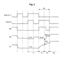
- FIG. 3 is a waveform diagram illustrating the signals EM, SCAN, INIT, and DATA applied to the pixel P of FIG. 2 and a change of the potential of the gate electrode and source electrode of the driving transistor DT.
- an operation of the pixel P in accordance with an embodiment of the present invention may include an initialization period Ti in which the gate-source potential of the driving transistor DT is initialized to a specific voltage, a sampling period Ts in which the threshold voltage Vth of the driving transistor DT is detected and stored, a writing period Tw in which the data voltage Vdata is applied, and an emission period Te in which a driving current applied to the OLED is compensated for regardless of the threshold voltage Vth using the threshold voltage Vth and the data voltage Vdata.
- the second transistor T2 supplies the second node n2 with the initialization voltage Vini, supplied by the initialization line 14a, in response to the second scan signal Scan2. Accordingly, the source voltage Vs of the driving transistor DT, that is, the voltage of the second node n2, has the same potential as the initialization voltage Vini. Furthermore, the switching transistor ST supplies the first node n1 of the gate electrode of the driving transistor DT with the reference voltage Vref, supplied by the data line 14b, in response to the first scan signal Scan1. Accordingly, the gate voltage Vg of the driving transistor DT, that is, the voltage of the first node n1, has the same potential as the reference voltage Vref.
- the initialization voltage Vini supplied to the second node n2 initializes the pixel P to a specific level.
- the initialization voltage Vini is set as a voltage value smaller than the operating voltage of the OLED so that the OLED does not emit light.
- the initialization voltage Vini may be set as a value of -1 to +1 V.
- the switching transistor ST supplies the first node n1 with the reference voltage Vref, supplied by the data line 14b, in response to the first scan signal Scan1. Furthermore, the first transistor T1 supplies the driving voltage EVDD to the driving transistor DT in response to the emission control signal EM. In this case, the voltage Vg of the gate electrode of the driving transistor DT maintains the reference voltage Vref. Furthermore, when the second node n2 is in a floating state, an electric current flowing from the input terminal for the driving voltage EVDD to the first transistor T1 and the driving transistor DT is accumulated in a voltage at the second node n2.
- the voltage raised in the sampling period Ts is saturated to a voltage having an amount corresponding to a difference between the reference voltage Vref and the threshold voltage Vth of the driving transistor DT. That is, the potential between the gate and source electrodes of the driving transistor DT is the same as the threshold voltage Vth of the driving transistor DT through the sampling period Ts.
- the first and the second transistors T1 and T2 are turned off. Furthermore, when the switching transistor ST is turned on, the data voltage Vdata supplied by the data line 14b is supplied to the first node n1. In this case, a voltage at the second node n2 in the floating state is increased or decreased because the storage capacitor Cs and the auxiliary capacitor C1 are coupled at their ratio.
- the second transistor T2 and the switching transistor ST are turned off, and the first transistor T1 is turned on.
- the data voltage Vdata stored in the storage capacitor Cs is supplied to the OLED. Accordingly, the OLED emits light with luminance proportional to the data voltage Vdata.
- an electric current flows in the driving transistor DT by the voltages of the first node n1 and second node 2 determined in the writing period Tw. Accordingly, a desired electric current is supplied to the OLED, and the OLED device may control its luminance based on the data voltage Vdata.
- a voltage drop of the storage capacitor Cs can be suppressed because the switching transistor ST is formed of an oxide semiconductor transistor having a low off current.
- the off current of the switching transistor ST is an electric current that flows from the drain electrode of the switching transistor ST to the source electrode in the state in which the switching transistor ST has been turned off because the gate-source potential of the switching transistor ST is less than the threshold voltage Vth.
- the off current of the switching transistor ST causes a voltage drop of the storage capacitor Cs.
- Such a voltage drop of the storage capacitor Cs causes a change ⁇ Vgs of the gate-source potential of the driving transistor DT.
- the voltage drop of the storage capacitor Cs causes a reduction in the luminance of the OLED because the gate-source potential of the driving transistor DT determines the emission luminance of the OLED. That is, the off current of the switching transistor ST causes a reduction in the luminance of the OLED. If luminance is reduced during one frame period, a flicker phenomenon is generated when a frame is changed due to a difference between the reduced luminance and the initial luminance of a subsequent frame.
- FIG. 4(a) is a diagram illustrating the off current of the LTPS transistor depending on the gate-source potential
- FIG. 4(b) is a diagram illustrating the off current of the oxide semiconductor transistor depending on the gate-source potential.
- the off current of the oxide semiconductor transistor is very smaller than that of the LTPS transistor and may not be accurately measured in a measurement range or less of measurement equipment.
- the switching transistor ST according to an embodiment has a very low off current that may be negligible because it is formed of an oxide semiconductor. Accordingly, the OLED device in accordance with an embodiment of the present invention can suppress a flicker phenomenon attributable to the off current.
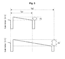
- FIG. 5 is a diagram illustrating a change of luminance between frames depending on the frequency.
- an emission period Te2 for low-frequency driving is longer than an emission period Te1 for standard frequency driving. Accordingly, a flicker problem is significantly reduced in low-frequency driving because a change of luminance ⁇ L' in low-frequency driving is greater than a change of luminance ⁇ L in standard frequency driving.
- a flicker phenomenon is not generated even in the case of low-frequency driving because the off current of the switching transistor ST is very small and thus a voltage drop of the storage capacitor Cs is very small.
- FIG. 6 (a) is a diagram illustrating a change of a flicker depending on a driving frequency, that is, a frame rate.
- FIG. 6(b) is a diagram illustrating a human sensitivity depending on a driving frequency.
- FIG. 6(c) is a diagram illustrating a change of a flicker that is felt by a person depending on a driving frequency as a result of the integration of FIGS. 6(a) and (b) .
- a first graph 1 illustrates a change of a flicker in a display device in which the switching transistor is made of low-temperature polysilicon
- a second graph 2 illustrates a change of a flicker in a display device in which the switching transistor is formed of an oxide semiconductor transistor in accordance with an embodiment of the present invention
- a difference of flicker between a first graph 1 and second graph 2 begins below driving frequency 40 Hz or less.
- the difference begins to increase in a driving frequency of 20 Hz or less and further increases in a driving frequency of 10 Hz or less.
- the display device in which the switching transistor is made of low-temperature polysilicon is applied to a display device having a driving frequency of 30 Hz or less, a flicker problem is occurred.
- the switching transistor ST is formed of an oxide semiconductor transistor as in an embodiment of the present invention (or in accordance with an embodiment described with respect to FIG. 8 below), a flicker is rarely generated although low-frequency driving close to a still image is performed.
- the human sensitivity is most sensitive in a driving frequency of 10 Hz, as illustrated in FIG. 6(b) .
- a flicker is suddenly decreased in a driving frequency of 10 Hz or less in the OLED device in accordance with an embodiment of the present invention.
- the flicker depending on the driving frequency as illustrated FIG. 6(a) may vary on a temperature.
- the effect in accordance with an embodiment of the present invention may be expected from the driving frequency of 30 Hz or less.
- a difference is generated from a driving frequency having a great change of a flicker between the display device using only low-temperature polysilicon and the display device using an oxide transistor as the switching transistor.
- a flicker is reduced more in the display device according to an embodiment of the present invention than in the display device using only low-temperature polysilicon from a driving frequency of 60 Hz or less.
- an embodiment of the present invention may be applied to a display device using a low-driving frequency in order to reduce consumption power because a flicker is not generated in a driving frequency having a low frame rate.
- an embodiment of the present invention may be applied to a case where a driving frequency is greatly reduced in order to reduce consumption power in portable display devices. For example, in the case of a portable electronic watch, if a display screen is changed for each second, a driving frequency of 1 Hz may be used. In an embodiment of the present invention, a flicker is rarely generated although a driving frequency that is 1 Hz or close to a still image is used.
- consumption power can be significantly reduced because a driving frequency can be greatly reduced when a still image is displayed as in the standby screen of a portable terminal.
- an embodiment of the present invention may be applied to a terminal not requiring a high driving frequency equivalent to a moving image level, such as an E-book, thereby greatly reducing consumption power. Accordingly, the portability of a portable terminal can be improved.
- a benefit of a display device including pixels including an ST and a DT as described herein is that the pixels of the display device can be driven at a frame rate (or refresh rate) at any frequency between 1-10, inclusive, while only rarely generating flicker.
- a frame rate or refresh rate
- the display device can also be driven normally at a more traditional frame rate such as at or near 60 Hz.
- the display device may switch operation as operational needs dictate between a relatively static, low power mode (e.g., 1 Hz frame rate), and a normal frame rate, higher power mode (e.g., 60 Hz frame rate).
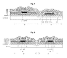
- FIG. 7 is a cross-sectional view illustrating the structure of the driving transistor DT and switching transistor ST in accordance with an embodiment of the present invention.
- the structure of the driving transistor DT and switching transistor ST and a method of forming the driving transistor DT and the switching transistor ST are described below with reference to FIG. 7 .
- a process of forming the driving transistor DT may include forming a buffer layer in a substrate.
- the buffer layer may be formed of an oxide (SiO 2 ) layer.
- a low-temperature polysilicon layer p-Si used as the active layer of the driving transistor DT may be formed on the buffer layer. Some region of the low-temperature polysilicon layer p-Si may be implemented into source and drain regions S and D through an ion injection process (also referred to as a charge carrier implantation process or charge carrier doping).
- a gate insulating layer GI may be formed on the low-temperature polysilicon layer p-Si.
- the gate insulating layer GI may be formed of an oxide (SiO 2 ) layer.
- a first gate layer Gate1 may be formed on the gate insulating layer GI.
- the gate may be made of a metal such as Molybdenum or Aluminum, or an alloy or combination of materials including a metal.
- one or more insulating layers may be sequentially formed to cover the first gate layer Gate1.
- the insulating layers include a first ILD and a second ILD.
- the insulating layers include a first, a second, and a third ILD.
- only a single insulation layer may be formed, or more than three insulation layers may be formed.
- a passivation layer PAS may be formed on the third insulating layer ILD3. Multiple insulating layers can prevent the current characteristics and reliability of transistor from being reduced.
- a process of forming the switching transistor ST may include forming a buffer layer in the substrate.
- a second gate layer Gate2 may be formed on the gate insulating layer GI.
- the third insulating layer ILD3 (or second ILD2 in an implementation where only two ILDs are used in the DT) may be formed to cover the second gate layer Gate2.
- An oxide semiconductor layer Active may be formed on the third insulating layer ILD3 (or, again ILD2 depending upon the implementation).
- the source and drain electrodes S and D may be formed in some region of the oxide semiconductor layer Active.
- the passivation layer PAS may be formed to cover the source electrode S and the drain electrode D.
- FIG. 8 is a cross-sectional view illustrating the structure of the driving transistor DT and switching transistor ST of the OLED device in accordance with another embodiment of the present invention.
- the same elements as those of the aforementioned embodiment are assigned the same reference numerals, and a detailed description thereof is omitted.
- the OLED device in accordance with another embodiment of the present invention uses low-temperature polysilicon transistors as both the driving transistor DT and the switching transistor ST.
- the channel width W2 of the switching transistor ST may be 5 ⁇ 15% (5 to 15%) smaller than the channel width W1 of the driving transistor DT.
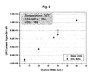
- the off current of the switching transistor ST and driving transistor DT is proportional to the channel width W2 of the switching transistor ST. Accordingly, in an embodiment of the present invention, the off current of the switching transistor ST can be reduced by setting the channel width W2 of the switching transistor ST smaller than the channel width W1 of the driving transistor DT.
- the off current of the switching transistor ST is reduced according to a reduction of the channel width W2 of the switching transistor ST, but the channel width W2 of the switching transistor ST may be set 5 ⁇ 15% narrower than the channel width W1 of the driving transistor DT so that reliability of driving is not affected.
- the doping concentration of the active layer p-Si of the switching transistor ST may be 5 ⁇ 15% higher than that of the active layer p-Si of the driving transistor DT.
- the off current of the switching transistor ST and driving transistor DT is in inverse proportion to the doping concentration of the switching transistor ST. The reason for this is that if the doping concentration of the active layer p-Si increases, resistance of a PN junction with a Lightly Doped Drain (LDD) region is increased and the off current is decreased.
- LDD Lightly Doped Drain
- the off current of the switching transistor ST can be reduced by setting the doping concentration of the active layer p-Si of the switching transistor ST higher than the doping concentration of the active layer p-Si of the driving transistor DT.
- the off current is decreased as the doping concentration of the switching transistor ST is increased, but the doping concentration of the active layer p-Si of the switching transistor ST may be set to be 5 ⁇ 15% higher than that of the active layer p-Si of the driving transistor DT so that reliability of driving is not affected.
- the thickness d2 of the active layer p-Si of the switching transistor ST may be 5 ⁇ 15% smaller than the thickness d1 of the active layer p-Si of the driving transistor DT.
- the off current of the switching transistor ST and driving transistor DT is proportional to the thickness d2 of the active layer p-Si. Accordingly, in an embodiment of the present invention, the off current can be reduced by setting the thickness d2 of the active layer of the switching transistor ST smaller than the thickness d1 of the active layer of the driving transistor DT.
- the off current is reduced as the thickness d2 of the active layer p-Si of the switching transistor ST is reduced, but the thickness d2 of the active layer p-Si of the switching transistor ST may be 5 ⁇ 15% smaller than the thickness d1 of the active layer p-Si of the driving transistor DT so that reliability of driving is not affected.
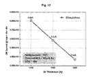
- the thickness (herein also referred to as height) h2 of the gate insulating layer GI of the switching transistor ST may be 5 ⁇ 15% greater than the thickness (herein also referred to as height) h1 of the gate insulating layer GI of the driving transistor DT.
- the off current of the switching transistor ST and driving transistor DT is in inverse proportion to the thickness of the gate insulating layer GI. Accordingly, in an embodiment of the present invention, the off current can be reduced by setting the thickness h2 of the gate insulating layer GI of the switching transistor ST greater than the thickness h1 of the gate insulating layer GI of the driving transistor DT.
- the off current is reduced as the thickness h2 of the gate insulating layer GI of the switching transistor ST is increased, but the thickness h2 of the gate insulating layer GI of the switching transistor ST may be 5 ⁇ 15% greater than the thickness h1 of the gate insulating layer GI the driving transistor DT so that reliability of driving is not affected.
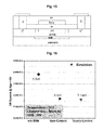
- FIGS. 13 , 15 , and 17 illustrate modification examples of the switching transistor ST using low-temperature polysilicon, an example of which is illustrated in FIG. 8 , described above.
- the doping concentration of a Lightly Doped Drain (LDD) region in the source and drain of the switching transistor ST may be 5 ⁇ 15% lower (e.g., less doping of additional n-type charge carriers) than that of the LDD region in the source and drain of the driving transistor DT (not shown in FIG. 13 ).
- the off current of the switching transistor ST and driving transistor DT is proportional to the doping concentration of the LDD region. The reason for this is that if the doping concentration of the LDD region increases, resistance of a junction with the active layer is reduced and thus the off current also increases.
- the off current can be reduced by setting the doping concentration of the LDD region of the switching transistor ST lower than that of the LDD region of the driving transistor DT.
- the off current is reduced as the doping concentration of the LDD region of the switching transistor ST is decreased, but the doping concentration of the LDD region of the switching transistor ST may be 5 ⁇ 15% lower than that of the LDD region of the driving transistor DT so that reliability of driving is not affected.
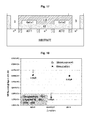
- the switching transistor ST may further include a Bottom Shield Metal (BSM) layer.
- BSM Bottom Shield Metal
- the BSM layer is formed under a channel layer with a buffer layer BUFFER interposed between the BSM layer and the channel layer.
- the BSM layer may be electrically connected to a gate Gate or a source/drain S, D.
- the BSM layer functions to reduce the off current by reducing an illumination effect that may affect the active layer of a device.
- the BSM layer functions to suppress the generation of carriers that may be introduced into the active layer in the off condition of the transistor due to a field distribution of a contact between the gate Gate and the source S. Accordingly, as illustrated in FIG. 16 , the off current of the switching transistor ST further including the BSM layer is reduced 6% or more. That is, the switching transistor ST in accordance with an embodiment of the present invention can further reduce the off current by additionally including the BSM layer.
- the switching transistor ST may be formed to have a dual gate electrode structure. From FIG. 18 , it may be seen that the off current of the switching transistor ST formed to have the dual gate electrode structure is 50% or more smaller than that of the driving transistor DT formed to have a single gate electrode structure. That is, the switching transistor ST in accordance with an embodiment of the present invention can reduce the off current using the switching transistor ST of a dual gate electrode structure.
- the low-temperature polysilicon switching transistor ST has a lower unit off current than the low-temperature polysilicon driving transistor DT when the unit off current, that is, an off current per unit length of the channel of the low-temperature polysilicon switching transistor ST is compared with that of the low-temperature polysilicon driving transistor DT because the switching transistor ST and the driving transistor DT have different channel lengths.
- the level of a flicker is in inverse proportion to capacitance of the storage capacitor Cs in addition to the off current. That is, a reduction of luminance attributable to the off current can be prevented because a voltage drop attributable to the off current can be reduced according to an increase of capacitance of the storage capacitor Cs.
- FIG. 19 is a diagram illustrating a first embodiment of the storage capacitor Cs in accordance with an embodiment of the present invention.
- the storage capacitor Cs has a structure in which a first metal layer 191, a first insulating layer GI, and a second metal layer 192 are sequentially stacked.
- the first metal layer 191 may be formed by making conductive the same semiconductor layer as the active layer Active of the driving transistor DT and switching transistor ST.
- the second metal layer 192 may be formed of the same metal layer as the gate layer Gate of the driving transistor DT and switching transistor ST.
- the first insulating layer GI may be formed using the same insulating layer as an insulating layer that covers the active layer Active of the driving transistor DT and switching transistor ST.
- the first insulating layer GI may be made of a substance having a high dielectric constant only in a region in which the storage capacitor Cs is formed. Hafnium Dioxide HfO2 and Zirconium Dioxide ZrO2 is used to achieve high dielectric constant. Accordingly, the storage capacitor Cs according to the first embodiment has a higher capacitance. A flicker can be improved because the storage capacitor Cs according to the first embodiment has high capacitance as described above.
- the gap between the first metal layer 191 and the second metal layer 192 may be narrow in order for the storage capacitor Cs according to the first embodiment to have high capacitance.
- FIG. 20 is a diagram illustrating a second embodiment of the storage capacitor Cs in accordance with an embodiment of the present invention.
- the storage capacitor Cs may include a first storage capacitor Cs and a second storage capacitor Cs stacked together.
- the first storage capacitor Cpa_1 may have a structure in which a first metal layer 191, a first insulating layer GI, and a second metal layer 192 are sequentially stacked.
- the first metal layer 191 may be formed of the same metal layer as the active layer of the driving transistor DT and switching transistor ST.
- the second metal layer 192 may be formed of the same metal layer as the gate layer Gate of the driving transistor DT and switching transistor ST.
- the first insulating layer GI may be formed of the same insulating layer that covers the active layer Active of the driving transistor DT and switching transistor ST.
- the second storage capacitor Cpa_2 may include a second metal layer 192, a second insulating layer ILD1, and a third metal layer 193.
- the second insulating layer ILD1 may be formed of the same insulating layer as an insulating layer that covers the gate Gate of the driving transistor DT and switching transistor ST.
- the third metal layer 193 may be made of the same metal layer as the source/drain electrode of the driving transistor DT and switching transistor ST.
- the storage capacitor Cs according to the second embodiment has high capacitance because it includes the first and the second capacitors Cpa_1 and Cpa2 connected in parallel. Accordingly, the storage capacitor Cs according to the second embodiment can improve a flicker because it has high capacitance.
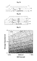
- FIG. 21 is a diagram illustrating that a flicker is changed depending on the off current when capacitance of the storage capacitor Cs is three times “ ⁇ 3" to five times “ ⁇ 5" greater than capacitance " ⁇ 1" of a common storage capacitor. From FIG. 21 , it may be seen that a flicker is reduced as capacitance of the storage capacitor is increased and the off current is reduced.
Landscapes
- Engineering & Computer Science (AREA)
- Physics & Mathematics (AREA)
- Computer Hardware Design (AREA)
- General Physics & Mathematics (AREA)
- Theoretical Computer Science (AREA)
- Geometry (AREA)
- Microelectronics & Electronic Packaging (AREA)
- Electroluminescent Light Sources (AREA)
- Chemical & Material Sciences (AREA)
- Crystallography & Structural Chemistry (AREA)
- Control Of El Displays (AREA)
Abstract
Description
- This application claims the priority benefit of Korean Patent Application No.
10-2014-0076096 filed on June 20, 2014 - The present invention relates to an organic light-emitting diode display device.
- A Flat Panel Display (FPD) is being widely used in portable computers, such as laptop computers and PDAs, and handheld telephone terminals as well as in the monitors of desktop computers due to advantages of a small size and light weight. Such an FPD may include a Liquid Crystal Display (LCD), a Plasma Display Panel (PDP), a Field Emission Display (FED), and an Organic Light Emitting Diode Display (hereinafter referred to as an OLED device).
- An OLED device is advantageous in that it has fast response speed, can represent luminance having high emission efficiency, and has a wide viewing angle. Owing to such many advantages, the OLED device is being used in various fields, such as portable displays including mobile phones and handheld electronic watches as well as large-screen display devices. Display devices used in various fields have different requirements, such as consumption power and reliability of driving suitable for the characteristics of their application fields. The pixel of a conventional OLED device does not suggest a functional structure corresponding to various requirements.
- An embodiment of the present invention is directed to the provision of an OLED device capable of satisfying various requirements depending on the characteristics of a field in which a display device is used.
- An embodiment of the present invention is directed to the provision of an active matrix OLED display device including an array of pixels, each pixel including an OLED, a driving transistor (DT) coupled to drive current through the OLED, a storage capacitor, and a switching transistor (also referred to as scanning transistor) (ST) coupled to control charge on the storage capacitor corresponding to a data voltage for said pixel. The display device also includes a timing controller configured to control the ST of each pixel to update the charge stored on the storage capacitor of each pixel at a frame rate including at least one frequency within a range of 1-10 Hertz (Hz). In an embodiment, each driving transistor (DT) comprises: a DT active layer formed on a substrate, the DT active layer formed of a low-temperature polysilicon material; a DT source and a DT drain both formed in the DT active layer; a gate insulating layer formed on the DT active layer; a DT gate formed on the gate insulating layer above the DT active layer; an insulating layer formed above the DT gate; wherein each switching transistor (ST) comprises: a ST gate formed on the gate insulating layer, the ST gate at least partially covered by the insulating layer; a ST active region formed on the insulating layer above the ST gate, the ST active layer formed of an oxide semiconductor material; and a ST source and a ST drain both contacting the ST active region on opposite sides of the ST gate; and wherein each OLED comprises an anode electrically coupled to the DT drain, and wherein the DT gate is electrically coupled to the ST source. In an embodiment, the oxide semiconductor material is at least one selected from the group consisting of: zinc oxide (ZnO) and Gallium Indium Zinc Oxide (GIZO). In an embodiment, both the DT gate and the ST gate are formed using a same metal layer. In an embodiment, the DT further comprises a first ILD formed on the DT gate; a second ILD formed on the first ILD; and wherein a third ILD is formed on the second ILD, and wherein the insulating layer is the third interlayer dielectric (ILD). In an embodiment, the DT further comprises: a first ILD formed on the DT gate; and a second ILD formed on the first ILD; and wherein the insulating layer is the second interlayer dielectric (ILD). In an embodiment, the insulating layer physically contacts the ST gate and the ST active layer. In an embodiment, the storage capacitor of each pixel further comprises a first layer formed with a portion of the DT active layer; a second layer formed with a portion of a metal layer, the metal layer also including the DT gate and the ST gate. In an embodiment, the first layer and the second layer are separated by a portion of the gate insulating layer, wherein the portion of the gate insulating layer between the first and the second layers is formed with a substance having a high dielectric constant. In an embodiment, each pixel further comprises: a second storage capacitor comprising: the second layer; and a third layer formed with a portion of a second metal layer, the second metal layer also including the DT source electrode and the DT drain electrode. In an embodiment, the second layer and the third layer are separated by a first interlayer dielectric (ILD) formed between the second layer and the third layer. In an embodiment, each driving transistor (DT) comprises: a DT active layer formed on a substrate having a thickness d1, the DT active layer formed of a low-temperature polysilicon material; a DT source and a DT drain both formed in the DT active layer; a gate insulating layer having a height h1 formed on the DT active layer; a DT gate having a channel width w1 formed on the gate insulating layer above the DT active layer; an insulating layer formed on the DT gate; wherein each switching transistor (ST) comprises: a ST active layer formed on the substrate having a thickness d2, the ST active layer formed of the low-temperature polysilicon material; a ST source and a ST drain both formed in the DT active layer; a ST gate having a channel width w2 formed on the gate insulating layer above the ST active layer, a portion of the insulating layer having a height h2 formed above the ST gate; wherein the OLED comprises an anode electrically coupled to the drain of the driving transistor, and wherein the DT gate is electrically coupled to the ST source; and wherein at least one of the height h2, the thickness d2, and the width w2 differs from the height h1, the thickness d1, and the width w1, respectively. In an embodiment, h2 is between 5-15% greater than h1. In an embodiment, w1 is between 5-15% greater than w2. In an embodiment, d1 is between 5-15% greater than d2. In an embodiment, the DT source and DT drain both comprise a first lightly doped drain (LDD) implantation of charge carriers i1; wherein the ST source and the ST drain both comprise a second LDD implantation of charge carriers i2; and wherein the concentration of charge carriers in i2 is lower than that in i1. In an embodiment, the ST comprises a dual gate structure, such that the ST gate comprises two physically separate portions, the ST active layer comprises two portions, and a portion of each active region on either side of both portions of the ST gate includes a lightly doped drain (LDD) implantation of charge carriers. In an embodiment, both the DT gate and the ST gate are formed using a same metal layer. In an embodiment, the DT further comprises: a first ILD formed on the DT gate; a second ILD formed on the first ILD; and wherein a third ILD is formed on the second ILD, and wherein the insulating layer is the third interlayer dielectric (ILD). In an embodiment, the DT further comprises: a first ILD formed on the DT gate; and a second ILD formed on the first ILD; and wherein the insulating layer is the second interlayer dielectric (ILD).
- The accompanying drawings, which are included to provide a further understanding of the invention and are incorporated in and constitute a part of this specification, illustrate embodiments of the invention and together with the description serve to explain the principles of the invention. In the drawings:
-
FIG. 1 is a diagram illustrating an OLED device in accordance with an embodiment of the present invention. -
FIG. 2 is a diagram illustrating an embodiment of a pixel included in the OLED device in accordance with an embodiment of the present invention. -
FIG. 3 is a timing diagram illustrating that the OLED device is driven in accordance with an embodiment of the present invention. -
FIGS. 4a and 4b are diagrams illustrating the off currents of a low-temperature polysilicon transistor and oxide semiconductor transistor. -
FIG. 5 is a diagram illustrating a change of luminance depending on a frame rate. -
FIG. 6 is a diagram illustrating a change of a flicker depending on a frame rate. -
FIG. 7 is a cross-sectional view illustrating the structure of a driving transistor and switching transistor in accordance with an embodiment of the present invention. -
FIG. 8 is a cross-sectional view illustrating the structure of a driving transistor and switching transistor in accordance with another embodiment of the present invention. -
FIG. 9 is a diagram illustrating a change of the off current depending on the channel width of the switching transistor. -
FIG. 10 is a diagram illustrating a change of the off current depending on the channel doping of the switching transistor. -
FIG. 11 is a diagram illustrating a change of the off current depending on the thickness of the active layer of the switching transistor. -
FIG. 12 is a diagram illustrating a change of the off current depending on the thickness of the gate insulating layer of the switching transistor. -
FIG. 13 is a cross-sectional view illustrating an embodiment of the switching transistor. -
FIG. 14 is a diagram illustrating a change of the off current depending on the doping concentration of the LDD of the switching transistor. -
FIG. 15 is a cross-sectional view illustrating another embodiment of the switching transistor. -
FIG. 16 is a diagram illustrating a change of the off current depending on whether the bottom shield metal of the switching transistor is present or not. -
FIG. 17 is a cross-sectional view illustrating yet another embodiment of the switching transistor. -
FIG. 18 is a diagram illustrating a difference in the off current between a dual gate structure and a single gate structure. -
FIG. 19 is a diagram illustrating a first embodiment of a storage capacitor in accordance with an embodiment of the present invention. -
FIG. 20 is a diagram illustrating a second embodiment of the storage capacitor in accordance with an embodiment of the present invention. -
FIG. 21 is a diagram illustrating a change of the off current depending on the capacitance of a storage capacitor. - Reference will now be made in detail to embodiments of the invention, examples of which are illustrated in the accompanying drawings. Wherever possible, the same reference numbers will be used throughout the drawings to refer to the same or like parts. It will be paid attention that detailed description of known arts will be omitted if it is determined that the arts can mislead the embodiments of the invention.
-
FIG. 1 is a diagram illustrating an OLED device in accordance with an embodiment of the present invention. - Referring to
FIG. 1 , the OLED device in accordance with an embodiment of the present invention may include adisplay panel 10 in which pixels P are arranged in a matrix form, adata driving circuit 12, agate driving circuit 13, and atiming controller 11. - The
display panel 10 includes a plurality of the pixels P and represents an image based on gray levels displayed by the respective pixels P. A plurality of the pixels P is arranged in each of horizontal lines at specific intervals and disposed in an active matrix form within thedisplay panel 10. - In this case, each of the pixels P is disposed in an area in which a
data line unit 14 and a plurality ofgate line units 15 orthogonal to each other are intersected. Each of thedata line units 14 connected to the pixels P may include aninitialization line 14a and adata line 14b. Each of thegate line units 15 connected to the pixels P may include afirst scan line 15a, asecond scan line 15b, and anemission line 15c. - Furthermore, each of the pixels P may include an OLED, a driving transistor DT, a switching transistor ST, first and second transistors T1 and T2, a storage capacitor Cs, and an auxiliary capacitor C1, as illustrated in
FIG. 2 . - The
timing controller 11 functions to control driving timing of thedata driving circuit 12 and thegate driving circuit 13. To this end, thetiming controller 11 may rearrange external digital video data RGB according to resolution of thedisplay panel 10 and supply the rearranged video data to thedata driving circuit 12. Furthermore, thetiming controller 11 generates a data control signal DDC for controlling operating timing of thedata driving circuit 12 and a gate control signal GDC for controlling operating timing of thegate driving circuit 13 based on timing signals, such as a vertical sync signal Vsync, a horizontal sync signal Hsync, a dot clock signal DCLK, and a data enable signal DE. - Consequently, the
timing controller 11 controls the frame rate, or rate at which the image projected by each pixel in the display is updated based on the charge maintained on the storage capacitor, as dictated by thedata driving circuit 12 described immediately below. Thus, if for example thetiming controller 11 is configured to update the pixels at a frame rate of 1 Hz, then thetiming controller 11 will cause the images projected by all of the pixels in the display once per second. - The
data driving circuit 12 functions to drive thedata line unit 14. To this end, thedata driving circuit 12 may convert the digital video data RGB, received from thetiming controller 11, into an analog data voltage in response to the data control signal DDC and supply the converted analog data voltage to the data lines 14. - The
gate driving circuit 13 functions to drive thegate line units 15. To this end, thegate driving circuit 13 may generate a scan signal, an emission control signal, and an initialization signal in response to the gate control signal GDC. Thegate driving circuit 13 supplies the scan signal to thescan lines 15a in a line-sequential manner, supplies the emission control signal to theemission lines 15b in a line-sequential manner, and supplies the initialization signal to theinitialization lines 15c in a line-sequential manner. -
FIG. 2 illustrates an example of the pixel P illustrated inFIG. 1 and illustrates one of the pixels P in the horizontal line. - Referring to
FIG. 2 , the pixel P in accordance with an embodiment of the present invention may include the OLED, the driving transistor DT, the switching transistor ST, the first and the second transistors T1 and T2, the storage capacitor Cs, and the auxiliary capacitor C1. - The OLED emits light in response to a driving current supplied by the driving transistor DT. A multilayer organic compound layer is formed between the anode electrode and cathode electrode of the OLED. The organic compound layer includes a Hole Injection Layer (HIL), a Hole Transport Layer (HTL), an emission Layer (EML), an Electron Transport Layer (ETL), and an Electron Injection Layer (EIL). The anode electrode of the OLED is connected to the source electrode of the driving transistor DT, and the cathode electrode thereof is connected to a low-voltage driving voltage EVSS.
- The driving transistor DT controls a driving current applied to the OLED using its own gate-source voltage. To this end, the gate electrode of the driving transistor DT may be connected to an input terminal for a data voltage Vdata, the drain electrode of the driving transistor DT may be connected to an input terminal for a driving voltage EVDD, and the source electrode of the driving transistor DT may be connected to the low-voltage driving voltage EVSS.
- The first transistor T1 controls a current path between the input terminal for the driving voltage EVDD and the driving transistor DT in response to an emission control signal EM. To this end, the gate electrode of the first transistor T1 may be connected to the
emission line 15c, the drain electrode of the first transistor T1 may be connected to the input terminal for the driving voltage EVDD, and the source electrode of the first transistor T1 may be connected to the driving transistor DT. - The second transistor T2 supplies a second node n2 with an initialization voltage Vini, supplied by the
initialization line 14a, in response to a second scan signal Scan2, that is, the scan signal of an (n-1)th horizontal line. To this end, the gate electrode of the second transistor T2 may be connected to an (n-1)thscan line 15a, the drain electrode of the second transistor T2 may be connected to theinitialization line 14a, and the source electrode of the second transistor T2 may be connected to the second node n2. - The driving transistor DT and the first and the second transistors T1 and T2 are formed of transistors using Low-Temperature PolySilicon (LTPS). The LTPS transistor can implement a high-performance display device because it has a high electron mobility and excellent reliability.
- The switching transistor ST supplies the driving transistor DT with a reference voltage Vref or the data voltage Vdata, supplied by the
data line 14b, in response to a first scan signal Scan1, that is, the scan signal of an nth horizontal line. To this end, the gate electrode of the switching transistor ST may be connected to the first scan line Scan1, the drain electrode of the switching transistor ST may be connected to thedata line 14b, and the source electrode of the switching transistor ST may be connected to the driving transistor DT. - The switching transistor ST is formed of an oxide transistor using an oxide semiconductor, such as zinc oxide (ZnO) or GaInZnO (GIZO), as an active layer. Since the oxide transistor has a low off current, the switching transistor ST using the oxide transistor can prevent the gate-source potential of the driving transistor DT from being reduced due to the off current. Accordingly, even in the case of low-frequency driving, a flicker can be prevented from occurring due to a reduction in the gate-source potential of the driving transistor DT attributable to the off current.
- The storage capacitor Cs maintains the data voltage Vdata provided by the
data line 14b for one frame so that the driving transistor DT maintains a constant voltage. To this end, the storage capacitor Cs may be connected to the gate electrode and source electrode of the driving transistor DT. The auxiliary capacitor C1 is connected in series to the storage capacitor Cs in the second node n2, thereby improving efficiency of the driving voltage Vdata. - An operation of the pixel P configured as described above is described below.
FIG. 3 is a waveform diagram illustrating the signals EM, SCAN, INIT, and DATA applied to the pixel P ofFIG. 2 and a change of the potential of the gate electrode and source electrode of the driving transistor DT. - Referring to
FIG. 3 , an operation of the pixel P in accordance with an embodiment of the present invention may include an initialization period Ti in which the gate-source potential of the driving transistor DT is initialized to a specific voltage, a sampling period Ts in which the threshold voltage Vth of the driving transistor DT is detected and stored, a writing period Tw in which the data voltage Vdata is applied, and an emission period Te in which a driving current applied to the OLED is compensated for regardless of the threshold voltage Vth using the threshold voltage Vth and the data voltage Vdata. - In the initialization period Ti, the second transistor T2 supplies the second node n2 with the initialization voltage Vini, supplied by the
initialization line 14a, in response to the second scan signal Scan2. Accordingly, the source voltage Vs of the driving transistor DT, that is, the voltage of the second node n2, has the same potential as the initialization voltage Vini. Furthermore, the switching transistor ST supplies the first node n1 of the gate electrode of the driving transistor DT with the reference voltage Vref, supplied by thedata line 14b, in response to the first scan signal Scan1. Accordingly, the gate voltage Vg of the driving transistor DT, that is, the voltage of the first node n1, has the same potential as the reference voltage Vref. - In the initialization period Ti, the initialization voltage Vini supplied to the second node n2 initializes the pixel P to a specific level. In this case, the initialization voltage Vini is set as a voltage value smaller than the operating voltage of the OLED so that the OLED does not emit light. For example, the initialization voltage Vini may be set as a value of -1 to +1 V.
- In the sampling period Ts, the switching transistor ST supplies the first node n1 with the reference voltage Vref, supplied by the
data line 14b, in response to the first scan signal Scan1. Furthermore, the first transistor T1 supplies the driving voltage EVDD to the driving transistor DT in response to the emission control signal EM. In this case, the voltage Vg of the gate electrode of the driving transistor DT maintains the reference voltage Vref. Furthermore, when the second node n2 is in a floating state, an electric current flowing from the input terminal for the driving voltage EVDD to the first transistor T1 and the driving transistor DT is accumulated in a voltage at the second node n2. The voltage raised in the sampling period Ts is saturated to a voltage having an amount corresponding to a difference between the reference voltage Vref and the threshold voltage Vth of the driving transistor DT. That is, the potential between the gate and source electrodes of the driving transistor DT is the same as the threshold voltage Vth of the driving transistor DT through the sampling period Ts. - In the writing period Tw, the first and the second transistors T1 and T2 are turned off. Furthermore, when the switching transistor ST is turned on, the data voltage Vdata supplied by the
data line 14b is supplied to the first node n1. In this case, a voltage at the second node n2 in the floating state is increased or decreased because the storage capacitor Cs and the auxiliary capacitor C1 are coupled at their ratio. - In the emission period Te, the second transistor T2 and the switching transistor ST are turned off, and the first transistor T1 is turned on. In the emission period Te, the data voltage Vdata stored in the storage capacitor Cs is supplied to the OLED. Accordingly, the OLED emits light with luminance proportional to the data voltage Vdata. In this case, an electric current flows in the driving transistor DT by the voltages of the first node n1 and
second node 2 determined in the writing period Tw. Accordingly, a desired electric current is supplied to the OLED, and the OLED device may control its luminance based on the data voltage Vdata. - In the process of the OLED emitting light, a voltage drop of the storage capacitor Cs can be suppressed because the switching transistor ST is formed of an oxide semiconductor transistor having a low off current.
- The off current of the switching transistor ST is an electric current that flows from the drain electrode of the switching transistor ST to the source electrode in the state in which the switching transistor ST has been turned off because the gate-source potential of the switching transistor ST is less than the threshold voltage Vth. The off current of the switching transistor ST causes a voltage drop of the storage capacitor Cs. Such a voltage drop of the storage capacitor Cs causes a change ΔVgs of the gate-source potential of the driving transistor DT. The voltage drop of the storage capacitor Cs causes a reduction in the luminance of the OLED because the gate-source potential of the driving transistor DT determines the emission luminance of the OLED. That is, the off current of the switching transistor ST causes a reduction in the luminance of the OLED. If luminance is reduced during one frame period, a flicker phenomenon is generated when a frame is changed due to a difference between the reduced luminance and the initial luminance of a subsequent frame.
-
FIG. 4(a) is a diagram illustrating the off current of the LTPS transistor depending on the gate-source potential, andFIG. 4(b) is a diagram illustrating the off current of the oxide semiconductor transistor depending on the gate-source potential. The off current of the oxide semiconductor transistor is very smaller than that of the LTPS transistor and may not be accurately measured in a measurement range or less of measurement equipment. As illustrated inFIG. 4(b) , the switching transistor ST according to an embodiment has a very low off current that may be negligible because it is formed of an oxide semiconductor. Accordingly, the OLED device in accordance with an embodiment of the present invention can suppress a flicker phenomenon attributable to the off current. - Accordingly, the OLED device in accordance with an embodiment of the present invention can provide a display device in which a flicker phenomenon is not generated even in the case of low-frequency driving.
FIG. 5 is a diagram illustrating a change of luminance between frames depending on the frequency. As illustrate inFIG. 5 , an emission period Te2 for low-frequency driving is longer than an emission period Te1 for standard frequency driving. Accordingly, a flicker problem is significantly reduced in low-frequency driving because a change of luminance ΔL' in low-frequency driving is greater than a change of luminance ΔL in standard frequency driving. - In an embodiment of the present invention, a flicker phenomenon is not generated even in the case of low-frequency driving because the off current of the switching transistor ST is very small and thus a voltage drop of the storage capacitor Cs is very small.
-
FIG. 6 (a) is a diagram illustrating a change of a flicker depending on a driving frequency, that is, a frame rate.FIG. 6(b) is a diagram illustrating a human sensitivity depending on a driving frequency.FIG. 6(c) is a diagram illustrating a change of a flicker that is felt by a person depending on a driving frequency as a result of the integration ofFIGS. 6(a) and (b) . - In
FIGS. 6(a) and (c) , afirst graph ① illustrates a change of a flicker in a display device in which the switching transistor is made of low-temperature polysilicon, and asecond graph ② illustrates a change of a flicker in a display device in which the switching transistor is formed of an oxide semiconductor transistor in accordance with an embodiment of the present invention. As illustrated inFIG. 6(a) , in the display device in which the switching transistor is made of low-temperature polysilicon, if a driving frequency is 30 Hz or less, a flicker suddenly increases as the driving frequency decreases. In contrast, in the display device in which the switching transistor ST is formed of the oxide semiconductor transistor, a flicker is decreased as a driving frequency is decreased. A difference of flicker between afirst graph ① andsecond graph ② begins below drivingfrequency 40 Hz or less. The difference begins to increase in a driving frequency of 20 Hz or less and further increases in a driving frequency of 10 Hz or less. As a result, if the display device in which the switching transistor is made of low-temperature polysilicon is applied to a display device having a driving frequency of 30 Hz or less, a flicker problem is occurred. - However, in the display device in which the switching transistor ST is formed of an oxide semiconductor transistor as in an embodiment of the present invention (or in accordance with an embodiment described with respect to
FIG. 8 below), a flicker is rarely generated although low-frequency driving close to a still image is performed. - Furthermore, the human sensitivity is most sensitive in a driving frequency of 10 Hz, as illustrated in
FIG. 6(b) . FromFIG. 6(b) , it may be seen that a flicker is suddenly decreased in a driving frequency of 10 Hz or less in the OLED device in accordance with an embodiment of the present invention. The flicker depending on the driving frequency as illustratedFIG. 6(a) may vary on a temperature. For example, as illustrated inFIG. 6(a) , at room temperature, the effect in accordance with an embodiment of the present invention may be expected from the driving frequency of 30 Hz or less. In contrast, at high temperature, a difference is generated from a driving frequency having a great change of a flicker between the display device using only low-temperature polysilicon and the display device using an oxide transistor as the switching transistor. For example, at high temperature, a flicker is reduced more in the display device according to an embodiment of the present invention than in the display device using only low-temperature polysilicon from a driving frequency of 60 Hz or less. - As described above, an embodiment of the present invention may be applied to a display device using a low-driving frequency in order to reduce consumption power because a flicker is not generated in a driving frequency having a low frame rate. In particular, an embodiment of the present invention may be applied to a case where a driving frequency is greatly reduced in order to reduce consumption power in portable display devices. For example, in the case of a portable electronic watch, if a display screen is changed for each second, a driving frequency of 1 Hz may be used. In an embodiment of the present invention, a flicker is rarely generated although a driving frequency that is 1 Hz or close to a still image is used. Furthermore, in an embodiment of the present invention, consumption power can be significantly reduced because a driving frequency can be greatly reduced when a still image is displayed as in the standby screen of a portable terminal.
- Furthermore, an embodiment of the present invention may be applied to a terminal not requiring a high driving frequency equivalent to a moving image level, such as an E-book, thereby greatly reducing consumption power. Accordingly, the portability of a portable terminal can be improved.
- Thus, in one embodiment, a benefit of a display device including pixels including an ST and a DT as described herein is that the pixels of the display device can be driven at a frame rate (or refresh rate) at any frequency between 1-10, inclusive, while only rarely generating flicker. This is advantageous, as it allows for creation of a comparatively static display device that consumes very little power. Additionally, the display device can also be driven normally at a more traditional frame rate such as at or near 60 Hz. As a result, the display device may switch operation as operational needs dictate between a relatively static, low power mode (e.g., 1 Hz frame rate), and a normal frame rate, higher power mode (e.g., 60 Hz frame rate).
-
FIG. 7 is a cross-sectional view illustrating the structure of the driving transistor DT and switching transistor ST in accordance with an embodiment of the present invention. The structure of the driving transistor DT and switching transistor ST and a method of forming the driving transistor DT and the switching transistor ST are described below with reference toFIG. 7 . - A process of forming the driving transistor DT may include forming a buffer layer in a substrate. The buffer layer may be formed of an oxide (SiO2) layer. A low-temperature polysilicon layer p-Si used as the active layer of the driving transistor DT may be formed on the buffer layer. Some region of the low-temperature polysilicon layer p-Si may be implemented into source and drain regions S and D through an ion injection process (also referred to as a charge carrier implantation process or charge carrier doping). A gate insulating layer GI may be formed on the low-temperature polysilicon layer p-Si. The gate insulating layer GI may be formed of an oxide (SiO2) layer. A first gate layer Gate1 may be formed on the gate insulating layer GI. The gate may be made of a metal such as Molybdenum or Aluminum, or an alloy or combination of materials including a metal.
- Thereafter, one or more insulating layers (also referred to as interlayer dielectrics or ILDs) may be sequentially formed to cover the first gate layer Gate1. In one implementation, the insulating layers include a first ILD and a second ILD. In another implementation, the insulating layers include a first, a second, and a third ILD. In other implementations, only a single insulation layer may be formed, or more than three insulation layers may be formed. Furthermore, a passivation layer PAS may be formed on the third insulating layer ILD3. Multiple insulating layers can prevent the current characteristics and reliability of transistor from being reduced.
- A process of forming the switching transistor ST may include forming a buffer layer in the substrate. A second gate layer Gate2 may be formed on the gate insulating layer GI. The third insulating layer ILD3 (or second ILD2 in an implementation where only two ILDs are used in the DT) may be formed to cover the second gate layer Gate2. An oxide semiconductor layer Active may be formed on the third insulating layer ILD3 (or, again ILD2 depending upon the implementation). The source and drain electrodes S and D may be formed in some region of the oxide semiconductor layer Active. The passivation layer PAS may be formed to cover the source electrode S and the drain electrode D.
-
FIG. 8 is a cross-sectional view illustrating the structure of the driving transistor DT and switching transistor ST of the OLED device in accordance with another embodiment of the present invention. In the present embodiment, the same elements as those of the aforementioned embodiment are assigned the same reference numerals, and a detailed description thereof is omitted. - Referring to
FIG. 8 , the OLED device in accordance with another embodiment of the present invention uses low-temperature polysilicon transistors as both the driving transistor DT and the switching transistor ST. - The channel width W2 of the switching transistor ST may be 5~15% (5 to 15%) smaller than the channel width W1 of the driving transistor DT. As illustrated in
FIG. 9 , the off current of the switching transistor ST and driving transistor DT is proportional to the channel width W2 of the switching transistor ST. Accordingly, in an embodiment of the present invention, the off current of the switching transistor ST can be reduced by setting the channel width W2 of the switching transistor ST smaller than the channel width W1 of the driving transistor DT. The off current of the switching transistor ST is reduced according to a reduction of the channel width W2 of the switching transistor ST, but the channel width W2 of the switching transistor ST may be set 5~15% narrower than the channel width W1 of the driving transistor DT so that reliability of driving is not affected. - The doping concentration of the active layer p-Si of the switching transistor ST may be 5~15% higher than that of the active layer p-Si of the driving transistor DT. As illustrated in
FIG. 10 , the off current of the switching transistor ST and driving transistor DT is in inverse proportion to the doping concentration of the switching transistor ST. The reason for this is that if the doping concentration of the active layer p-Si increases, resistance of a PN junction with a Lightly Doped Drain (LDD) region is increased and the off current is decreased. Accordingly, in an embodiment of the present invention, the off current of the switching transistor ST can be reduced by setting the doping concentration of the active layer p-Si of the switching transistor ST higher than the doping concentration of the active layer p-Si of the driving transistor DT. The off current is decreased as the doping concentration of the switching transistor ST is increased, but the doping concentration of the active layer p-Si of the switching transistor ST may be set to be 5~15% higher than that of the active layer p-Si of the driving transistor DT so that reliability of driving is not affected. - The thickness d2 of the active layer p-Si of the switching transistor ST may be 5~15% smaller than the thickness d1 of the active layer p-Si of the driving transistor DT. As illustrated in
FIG. 11 , the off current of the switching transistor ST and driving transistor DT is proportional to the thickness d2 of the active layer p-Si. Accordingly, in an embodiment of the present invention, the off current can be reduced by setting the thickness d2 of the active layer of the switching transistor ST smaller than the thickness d1 of the active layer of the driving transistor DT. The off current is reduced as the thickness d2 of the active layer p-Si of the switching transistor ST is reduced, but the thickness d2 of the active layer p-Si of the switching transistor ST may be 5~15% smaller than the thickness d1 of the active layer p-Si of the driving transistor DT so that reliability of driving is not affected. - The thickness (herein also referred to as height) h2 of the gate insulating layer GI of the switching transistor ST may be 5~15% greater than the thickness (herein also referred to as height) h1 of the gate insulating layer GI of the driving transistor DT. As illustrated in
FIG. 12 , the off current of the switching transistor ST and driving transistor DT is in inverse proportion to the thickness of the gate insulating layer GI. Accordingly, in an embodiment of the present invention, the off current can be reduced by setting the thickness h2 of the gate insulating layer GI of the switching transistor ST greater than the thickness h1 of the gate insulating layer GI of the driving transistor DT. The off current is reduced as the thickness h2 of the gate insulating layer GI of the switching transistor ST is increased, but the thickness h2 of the gate insulating layer GI of the switching transistor ST may be 5~15% greater than the thickness h1 of the gate insulating layer GI the driving transistor DT so that reliability of driving is not affected. -
FIGS. 13 ,15 , and17 illustrate modification examples of the switching transistor ST using low-temperature polysilicon, an example of which is illustrated inFIG. 8 , described above. - Referring to
FIG. 13 , in an embodiment of the present invention, the doping concentration of a Lightly Doped Drain (LDD) region in the source and drain of the switching transistor ST (adjacent to the active region labeled ACT inFIG. 13 ) may be 5~15% lower (e.g., less doping of additional n-type charge carriers) than that of the LDD region in the source and drain of the driving transistor DT (not shown inFIG. 13 ). As illustrated inFIG. 14 , the off current of the switching transistor ST and driving transistor DT is proportional to the doping concentration of the LDD region. The reason for this is that if the doping concentration of the LDD region increases, resistance of a junction with the active layer is reduced and thus the off current also increases. Accordingly, in an embodiment of the present invention, the off current can be reduced by setting the doping concentration of the LDD region of the switching transistor ST lower than that of the LDD region of the driving transistor DT. The off current is reduced as the doping concentration of the LDD region of the switching transistor ST is decreased, but the doping concentration of the LDD region of the switching transistor ST may be 5~15% lower than that of the LDD region of the driving transistor DT so that reliability of driving is not affected. - Referring to
FIG. 15 , the switching transistor ST may further include a Bottom Shield Metal (BSM) layer. The BSM layer is formed under a channel layer with a buffer layer BUFFER interposed between the BSM layer and the channel layer. Although not illustrated, the BSM layer may be electrically connected to a gate Gate or a source/drain S, D. The BSM layer functions to reduce the off current by reducing an illumination effect that may affect the active layer of a device. Furthermore, the BSM layer functions to suppress the generation of carriers that may be introduced into the active layer in the off condition of the transistor due to a field distribution of a contact between the gate Gate and the source S. Accordingly, as illustrated inFIG. 16 , the off current of the switching transistor ST further including the BSM layer is reduced 6% or more. That is, the switching transistor ST in accordance with an embodiment of the present invention can further reduce the off current by additionally including the BSM layer. - Referring to
FIG. 17 , the switching transistor ST may be formed to have a dual gate electrode structure. FromFIG. 18 , it may be seen that the off current of the switching transistor ST formed to have the dual gate electrode structure is 50% or more smaller than that of the driving transistor DT formed to have a single gate electrode structure. That is, the switching transistor ST in accordance with an embodiment of the present invention can reduce the off current using the switching transistor ST of a dual gate electrode structure. - As described above, in the aforementioned embodiments, a flicker can be improved by reducing the off current. In accordance with an embodiment of the present invention, the low-temperature polysilicon switching transistor ST has a lower unit off current than the low-temperature polysilicon driving transistor DT when the unit off current, that is, an off current per unit length of the channel of the low-temperature polysilicon switching transistor ST is compared with that of the low-temperature polysilicon driving transistor DT because the switching transistor ST and the driving transistor DT have different channel lengths.
- The level of a flicker is in inverse proportion to capacitance of the storage capacitor Cs in addition to the off current. That is, a reduction of luminance attributable to the off current can be prevented because a voltage drop attributable to the off current can be reduced according to an increase of capacitance of the storage capacitor Cs.
- Embodiments in which capacitance of the storage capacitor Cs has been improved in order to improve a flicker are described below.
-
FIG. 19 is a diagram illustrating a first embodiment of the storage capacitor Cs in accordance with an embodiment of the present invention. - Referring to
FIG. 19 , the storage capacitor Cs has a structure in which afirst metal layer 191, a first insulating layer GI, and asecond metal layer 192 are sequentially stacked. Thefirst metal layer 191 may be formed by making conductive the same semiconductor layer as the active layer Active of the driving transistor DT and switching transistor ST. Thesecond metal layer 192 may be formed of the same metal layer as the gate layer Gate of the driving transistor DT and switching transistor ST. The first insulating layer GI may be formed using the same insulating layer as an insulating layer that covers the active layer Active of the driving transistor DT and switching transistor ST. - The first insulating layer GI may be made of a substance having a high dielectric constant only in a region in which the storage capacitor Cs is formed. Hafnium Dioxide HfO2 and Zirconium Dioxide ZrO2 is used to achieve high dielectric constant. Accordingly, the storage capacitor Cs according to the first embodiment has a higher capacitance. A flicker can be improved because the storage capacitor Cs according to the first embodiment has high capacitance as described above.
- The gap between the
first metal layer 191 and thesecond metal layer 192 may be narrow in order for the storage capacitor Cs according to the first embodiment to have high capacitance. -
FIG. 20 is a diagram illustrating a second embodiment of the storage capacitor Cs in accordance with an embodiment of the present invention. - Referring to
FIG. 20 , the storage capacitor Cs according to the second embodiment may include a first storage capacitor Cs and a second storage capacitor Cs stacked together. The first storage capacitor Cpa_1 may have a structure in which afirst metal layer 191, a first insulating layer GI, and asecond metal layer 192 are sequentially stacked. Thefirst metal layer 191 may be formed of the same metal layer as the active layer of the driving transistor DT and switching transistor ST. Thesecond metal layer 192 may be formed of the same metal layer as the gate layer Gate of the driving transistor DT and switching transistor ST. The first insulating layer GI may be formed of the same insulating layer that covers the active layer Active of the driving transistor DT and switching transistor ST. The second storage capacitor Cpa_2 may include asecond metal layer 192, a second insulating layer ILD1, and athird metal layer 193. The second insulating layer ILD1 may be formed of the same insulating layer as an insulating layer that covers the gate Gate of the driving transistor DT and switching transistor ST. Furthermore, thethird metal layer 193 may be made of the same metal layer as the source/drain electrode of the driving transistor DT and switching transistor ST. - The storage capacitor Cs according to the second embodiment has high capacitance because it includes the first and the second capacitors Cpa_1 and Cpa2 connected in parallel. Accordingly, the storage capacitor Cs according to the second embodiment can improve a flicker because it has high capacitance.
-
FIG. 21 is a diagram illustrating that a flicker is changed depending on the off current when capacitance of the storage capacitor Cs is three times "×3" to five times "×5" greater than capacitance "×1" of a common storage capacitor. FromFIG. 21 , it may be seen that a flicker is reduced as capacitance of the storage capacitor is increased and the off current is reduced. - Although embodiments have been described with reference to a number of illustrative embodiments thereof, it should be understood that numerous other modifications and embodiments can be devised by those skilled in the art that will fall within the scope of the principles of this disclosure. More particularly, various variations and modifications are possible in the component parts and/or arrangements of the subject combination arrangement within the scope of the disclosure, the drawings and the appended claims. In addition to variations and modifications in the component parts and/or arrangements, alternative uses will also be apparent to those skilled in the art.
Claims (15)
- An organic light emitting diode (OLED) display device comprising:an active matrix OLED array comprising a plurality of pixels (P) arranged in a row and column structure, each pixel (P) comprising an OLED, a driving transistor - hereinafter abbreviated as "DT" - coupled to drive current through the OLED, a storage capacitor (Cs), and a switching transistor - hereinafter abbreviated as "ST" - coupled to control charge on the storage capacitor (Cs) corresponding to a data voltage for said pixel (P); anda timing controller (11) configured to control the ST of each pixel (P) to update the charge stored on the storage capacitor (Cs) of each pixel (P) at a frame rate including at least one frequency within a range of 1-10 Hertz (Hz).
- The OLED display device of claim 1,
wherein each driving transistor comprises:a DT active layer formed on a substrate, the DT active layer formed of a low-temperature polysilicon material;a DT source and a DT drain both formed in the DT active layer;a gate insulating layer (GI) formed on the DT active layer;a DT gate (GATE1) formed on the gate insulating layer above the DT active layer;an insulating layer formed above the DT gate (GATE1);wherein each switching transistor (ST) comprises:a ST gate (Gate2) formed on the gate insulating layer (GI), the ST gate (Gate2) at least partially covered by the insulating layer;a ST active region formed on the insulating layer above the ST gate (Gate2), the ST active layer formed of an oxide semiconductor material; anda ST source and a ST drain both contacting the ST active region on opposite sides of the ST gate (Gate2); andwherein each OLED comprises an anode electrically coupled to the DT drain, and wherein the DT gate (GATE1) is electrically coupled to the ST source,
wherein, preferably, the oxide semiconductor material is at least one selected from the group consisting of: zinc oxide (ZnO) and Gallium Indium Zinc Oxide (GIZO). - The OLED display device of claim 2, wherein both the DT gate (GATE1) and the ST gate (Gate2) are formed using a same metal layer.
- The OLED display device of claim 2 or 3, wherein the DT further comprises:a first interlayer dielectric (ILD1) formed on the DT gate (GATE1);a second interlayer dielectric (ILD2) formed on the first interlayer dielectric (ILD1); andwherein a third interlayer dielectric (ILD3) is formed on the second interlayer dielectric (ILD2), andwherein the insulating layer is the third interlayer dielectric (ILD3).
- The OLED display device of claims 2 or 3, wherein the DT further comprises:a first interlayer dielectric (ILD1) formed on the DT gate (GATE1); anda second interlayer dielectric (ILD2) formed on the first interlayer dielectric (ILD1); andwherein the insulating layer is the second interlayer dielectric (ILD2).
- The OLED display device of any one of claims 2 to 5, wherein the insulating layer physically contacts the ST gate (Gate2) and the ST active layer.
- The OLED display device of claim 2 or 3, wherein the storage capacitor (Cs) of each pixel (P) further comprises:a first layer (191) formed with a portion of the DT active layer;
a second layer (192) formed with a portion of a metal layer, the metal layer also including the DT gate (GATE1) and the ST gate (Gate2),
wherein, preferably, the first layer (191) and the second layer (192) are separated by a portion of the gate insulating layer (GI), wherein the portion of the gate insulating layer (GI) between the first and the second layers (191, 192) is formed with a substance having a high dielectric constant. - The OLED display device of claim 7, wherein each pixel (P) further comprises:a second storage capacitor (Cpa._2) comprising:the second layer (192); anda third layer (193) formed with a portion of a second metal layer, the second metal layer also including the DT source electrode and the DT drain electrode,wherein, preferably, the second layer (192) and the third layer (193) are separated by a first interlayer dielectric (ILD1) formed between the second layer (192) and the third layer (193).
- The OLED display device of claim 1,
wherein each driving transistor comprises:a DT active layer formed on a substrate having a thickness d1, the DT active layer formed of a low-temperature polysilicon material;a DT source and a DT drain both formed in the DT active layer;a gate insulating layer (GI) having a height h1 formed on the DT active layer;a DT gate (GATE) having a channel width w1 formed on the gate insulating layer above the DT active layer;an insulating layer formed on the DT gate (GATE);wherein each switching transistor comprises:a ST active layer formed on the substrate having thickness d2, the ST active layer formed of the low-temperature polysilicon material;a ST source and a ST drain both formed in the DT active layer;a ST gate (GATE) having a channel width w2 formed on the gate insulating layer (GI) above the ST active layer, a portion of the insulating layer having a height h2 formed above the ST gate (GATE);wherein the OLED comprises an anode electrically coupled to the drain of the driving transistor, and wherein the DT gate (GATE) is electrically coupled to the ST source; and
wherein at least one of the height h2, the thickness d2, and the width w2 differs from the height h1, the thickness d1, and the width w1, respectively,
wherein, preferably, both the DT gate (GATE) and the ST gate (GATE) are formed using a same metal layer. - The OLED display device of claim 9, wherein h2 is between 5-15% greater than h1.
- The OLED display device of claim 9 or 10, wherein w1 is between 5-15% greater than w2.
- The OLED display device of any one of claims 9 to 11, wherein d1 is between 5-15% greater than d2.
- The OLED display device of any one of claims 9 to 12,
wherein the DT source and DT drain both comprise a first lightly doped drain (LDD) implantation of charge carriers i1;
wherein the ST source and the ST drain both comprise a second lightly doped drain (LDD) implantation of charge carriers i2; and
wherein the concentration of charge carriers in i2 is lower than that in i1. - The OLED display device of any one of claims 9 to 13, wherein the ST comprises a dual gate structure, such that the ST gate (GATE) comprises two physically separate portions, the ST active layer comprises two portions, and a portion of each active region on either side of both portions of the ST gate includes a lightly doped drain (LDD) implantation of charge carriers.
- The OLED display device of any one of claims 9 to 14, wherein the DT further comprises:a first interlayer dielectric (ILD1) formed on the DT gate;a second interlayer dielectric (ILD2) formed on the first interlayer dielectric (ILD1);wherein a third interlayer dielectric (ILD3) is formed on the second interlayer dielectric (ILD2), andwherein the insulating layer is the third interlayer dielectric (ILD3);or wherein the DT further comprises:a first interlayer dielectric (ILD1) formed on the DT gate (GATE); anda second interlayer dielectric (ILD2) formed on the first interlayer dielectric (ILD1); andwherein the insulating layer is the second interlayer dielectric (ILD2).
Applications Claiming Priority (1)
| Application Number | Priority Date | Filing Date | Title |
|---|---|---|---|
| KR1020140076096A KR102298336B1 (en) | 2014-06-20 | 2014-06-20 | Organic Light Emitting diode Display |
Publications (1)
| Publication Number | Publication Date |
|---|---|
| EP2958102A1 true EP2958102A1 (en) | 2015-12-23 |
Family
ID=53434266
Family Applications (1)
| Application Number | Title | Priority Date | Filing Date |
|---|---|---|---|
| EP15172514.0A Ceased EP2958102A1 (en) | 2014-06-20 | 2015-06-17 | Reduced off current switching transistor in an organic light-emitting diode display device |
Country Status (4)
| Country | Link |
|---|---|
| US (2) | US9412303B2 (en) |
| EP (1) | EP2958102A1 (en) |
| KR (1) | KR102298336B1 (en) |
| CN (1) | CN105225633B (en) |
Families Citing this family (60)
| Publication number | Priority date | Publication date | Assignee | Title |
|---|---|---|---|---|
| KR102206287B1 (en) * | 2014-06-13 | 2021-01-25 | 삼성디스플레이 주식회사 | Display device and method of driving a display device |
| KR20160011248A (en) * | 2014-07-21 | 2016-02-01 | 삼성디스플레이 주식회사 | Display panel and organic light emitting display device having the same |
| CN106558593B (en) * | 2015-09-18 | 2019-12-17 | 鸿富锦精密工业(深圳)有限公司 | Array substrate, display panel, display device and method for preparing array substrate |
| WO2021035414A1 (en) | 2019-08-23 | 2021-03-04 | 京东方科技集团股份有限公司 | Pixel circuit and driving method therefor, and display substrate and driving method therefor, and display device |
| US11600234B2 (en) | 2015-10-15 | 2023-03-07 | Ordos Yuansheng Optoelectronics Co., Ltd. | Display substrate and driving method thereof |
| CN105185816A (en) | 2015-10-15 | 2015-12-23 | 京东方科技集团股份有限公司 | Array substrate, manufacturing method, and display device |
| KR102457757B1 (en) * | 2015-10-28 | 2022-10-24 | 삼성디스플레이 주식회사 | Pixel circuit and organic light emitting display device including the same |
| JP2017116576A (en) * | 2015-12-21 | 2017-06-29 | 株式会社ジャパンディスプレイ | Display device |
| CN105489615B (en) * | 2016-01-13 | 2019-03-08 | 深圳市华星光电技术有限公司 | Thin film transistor array substrate for AMOLED and manufacturing method thereof |
| WO2017183355A1 (en) * | 2016-04-22 | 2017-10-26 | ソニー株式会社 | Display apparatus and electronic device |
| KR102617379B1 (en) | 2016-05-02 | 2023-12-27 | 삼성디스플레이 주식회사 | Organic light emitting display apparatus and manufacturing method thereof |
| JP6668160B2 (en) * | 2016-05-06 | 2020-03-18 | 株式会社ジャパンディスプレイ | Display device manufacturing method |
| DE112017003050B4 (en) | 2016-06-20 | 2026-05-07 | Sony Corporation | Display device and electronic device |
| KR20180004370A (en) * | 2016-07-01 | 2018-01-11 | 삼성디스플레이 주식회사 | Pixel and stage circuit and organic light emitting display device having the pixel and the stage circuit |
| KR102561294B1 (en) | 2016-07-01 | 2023-08-01 | 삼성디스플레이 주식회사 | Pixel and stage circuit and organic light emitting display device having the pixel and the stage circuit |
| US10339855B2 (en) | 2016-08-30 | 2019-07-02 | Apple, Inc. | Device and method for improved LED driving |
| CN114155812A (en) * | 2016-08-30 | 2022-03-08 | 索尼半导体解决方案公司 | Display device and electronic apparatus |
| KR102795156B1 (en) * | 2016-08-31 | 2025-04-15 | 엘지디스플레이 주식회사 | Organic Light Emitting Display |
| JP2018063351A (en) * | 2016-10-13 | 2018-04-19 | 株式会社ジャパンディスプレイ | Organic el display device and method for driving organic el display device |
| KR102516721B1 (en) * | 2016-11-30 | 2023-03-30 | 엘지디스플레이 주식회사 | Transistor substrate, organic light emitting display panel using the same, method of manufacturing the same, and organic light emitting display apparatus using the same |
| KR102541552B1 (en) | 2016-11-30 | 2023-06-07 | 엘지디스플레이 주식회사 | Transistor substrate and organic light emitting display panel and organic light emitting display apparatus using the same |
| KR102566551B1 (en) | 2016-12-05 | 2023-08-14 | 삼성디스플레이주식회사 | Display device and method for driving the same |
| KR102775758B1 (en) | 2017-02-24 | 2025-03-07 | 삼성디스플레이 주식회사 | Pixel and organic light emitting display device having the pixel |
| US10672338B2 (en) * | 2017-03-24 | 2020-06-02 | Apple Inc. | Organic light-emitting diode display with external compensation and anode reset |
| KR102309097B1 (en) | 2017-04-10 | 2021-10-07 | 삼성디스플레이 주식회사 | Display device and method of driving the same |
| TWI620111B (en) * | 2017-05-19 | 2018-04-01 | 友達光電股份有限公司 | Display device and operating method thereof |
| CN107293552A (en) * | 2017-06-05 | 2017-10-24 | 深圳市华星光电技术有限公司 | A kind of array base palte and display device |
| KR102464131B1 (en) | 2017-06-30 | 2022-11-04 | 엘지디스플레이 주식회사 | Electroluminescence DISPLAY DEVICE |
| KR102462008B1 (en) * | 2017-09-22 | 2022-11-03 | 삼성디스플레이 주식회사 | Organic light emitting display device |
| CN107818991B (en) * | 2017-10-23 | 2020-06-05 | 京东方科技集团股份有限公司 | Array substrate and preparation method thereof, and display panel |
| KR102547410B1 (en) * | 2017-10-31 | 2023-06-22 | 엘지디스플레이 주식회사 | Light emitting display apparatus |
| KR102328441B1 (en) * | 2017-11-10 | 2021-11-17 | 엘지디스플레이 주식회사 | Organic light emitting display device |
| CN108257975B (en) * | 2018-01-02 | 2022-10-04 | 京东方科技集团股份有限公司 | Array substrate and preparation method thereof, display device and preparation method of thin film transistor |
| KR102509795B1 (en) | 2018-05-03 | 2023-03-15 | 삼성디스플레이 주식회사 | Display apparatus, method of driving display panel using the same |
| KR102565412B1 (en) | 2018-08-28 | 2023-08-10 | 삼성디스플레이 주식회사 | Organic light emitting display device |
| KR102482335B1 (en) * | 2018-10-04 | 2022-12-29 | 삼성디스플레이 주식회사 | Display apparatus, method of driving display panel using the same |
| CN109285502B (en) * | 2018-11-14 | 2020-06-16 | 武汉华星光电半导体显示技术有限公司 | OLED display panel |
| KR102583819B1 (en) * | 2018-12-18 | 2023-10-04 | 삼성디스플레이 주식회사 | Display apparatus, method of driving display panel using the same |
| KR102678855B1 (en) | 2019-01-28 | 2024-06-28 | 삼성디스플레이 주식회사 | Display apparatus and method of driving display panel using the same |
| KR102854478B1 (en) * | 2019-03-05 | 2025-09-03 | 삼성디스플레이 주식회사 | Display device and manufacturing method of the same |
| CN110299322B (en) * | 2019-07-03 | 2022-03-08 | 京东方科技集团股份有限公司 | Display substrate, manufacturing method thereof and display device |
| US11930664B2 (en) | 2019-08-23 | 2024-03-12 | Boe Technology Group Co., Ltd. | Display device with transistors oriented in directions intersecting direction of driving transistor and manufacturing method thereof |
| US12266303B2 (en) | 2019-08-23 | 2025-04-01 | Boe Technology Group Co., Ltd. | Display device and manufacturing method thereof |
| US11600681B2 (en) | 2019-08-23 | 2023-03-07 | Boe Technology Group Co., Ltd. | Display device and manufacturing method thereof |
| CN112840461B (en) | 2019-08-23 | 2025-02-25 | 京东方科技集团股份有限公司 | Display panel and manufacturing method thereof, and display device |
| EP4020572B1 (en) | 2019-08-23 | 2026-05-06 | BOE Technology Group Co., Ltd. | Display device and manufacturing method therefor |
| CN114694590B (en) * | 2019-08-23 | 2024-06-11 | 京东方科技集团股份有限公司 | Display device and method for manufacturing the same |
| US11404451B2 (en) | 2019-08-27 | 2022-08-02 | Boe Technology Group Co., Ltd. | Electronic device substrate, manufacturing method thereof, and electronic device |
| CN110707095A (en) * | 2019-09-04 | 2020-01-17 | 深圳市华星光电半导体显示技术有限公司 | display panel |
| CN118763123A (en) | 2019-09-24 | 2024-10-11 | 乐金显示有限公司 | Thin film transistor, substrate thereof, and display device including the thin film transistor |
| KR102615673B1 (en) * | 2019-12-26 | 2023-12-18 | 엘지디스플레이 주식회사 | Display device |
| CN111682047A (en) * | 2020-06-12 | 2020-09-18 | 福建华佳彩有限公司 | A compensation capacitor structure and a method for improving its capacitance |
| CN111627387B (en) | 2020-06-24 | 2022-09-02 | 京东方科技集团股份有限公司 | Pixel driving circuit and driving method thereof, display panel and display device |
| JP2022035402A (en) | 2020-08-20 | 2022-03-04 | シャープ株式会社 | Display device, display drive method, and display drive program |
| JP7030162B1 (en) | 2020-08-20 | 2022-03-04 | シャープ株式会社 | Control device, display device with self-luminous element, control method and control program |
| CN112034616B (en) * | 2020-08-31 | 2022-06-03 | 同济大学 | Variable lens for scalable low-energy laser ultra-high speed scanning and application |
| CN112071259B (en) * | 2020-09-15 | 2021-11-23 | 武汉华星光电半导体显示技术有限公司 | Pixel circuit and display panel |
| CN116097924A (en) * | 2021-03-11 | 2023-05-09 | 京东方科技集团股份有限公司 | Array substrate, display panel and display device thereof |
| CN113161404B (en) * | 2021-04-23 | 2023-04-18 | 武汉天马微电子有限公司 | Display panel and display device |
| CN116844472B (en) * | 2023-07-20 | 2026-01-23 | 京东方科技集团股份有限公司 | Pixel data processing method, device, display equipment and storage medium |
Citations (3)
| Publication number | Priority date | Publication date | Assignee | Title |
|---|---|---|---|---|
| US20110115839A1 (en) * | 2009-11-13 | 2011-05-19 | Semiconductor Energy Laboratory Co., Ltd. | Display device and electronic device including the same |
| US20140152630A1 (en) * | 2012-11-30 | 2014-06-05 | Semiconductor Energy Laboratory Co., Ltd. | Display device |
| EP2911201A1 (en) * | 2014-02-24 | 2015-08-26 | LG Display Co., Ltd. | Thin film transistor substrate and display using the same |
Family Cites Families (22)
| Publication number | Priority date | Publication date | Assignee | Title |
|---|---|---|---|---|
| TW591584B (en) * | 1999-10-21 | 2004-06-11 | Semiconductor Energy Lab | Active matrix type display device |
| JP3899886B2 (en) * | 2001-10-10 | 2007-03-28 | 株式会社日立製作所 | Image display device |
| US6852997B2 (en) * | 2001-10-30 | 2005-02-08 | Semiconductor Energy Laboratory Co., Ltd. | Light emitting device |
| US7915723B2 (en) * | 2004-01-29 | 2011-03-29 | Casio Computer Co., Ltd. | Transistor array, manufacturing method thereof and image processor |
| KR100600878B1 (en) * | 2004-06-29 | 2006-07-14 | 삼성에스디아이 주식회사 | Thin film transistor and its manufacturing method |
| US7646367B2 (en) * | 2005-01-21 | 2010-01-12 | Semiconductor Energy Laboratory Co., Ltd. | Semiconductor device, display device and electronic apparatus |
| US8681077B2 (en) * | 2005-03-18 | 2014-03-25 | Semiconductor Energy Laboratory Co., Ltd. | Semiconductor device, and display device, driving method and electronic apparatus thereof |
| KR20070081829A (en) * | 2006-02-14 | 2007-08-20 | 삼성전자주식회사 | OLED display and manufacturing method thereof |
| JP2008042010A (en) * | 2006-08-08 | 2008-02-21 | Sharp Corp | SEMICONDUCTOR DEVICE, SEMICONDUCTOR DEVICE MANUFACTURING METHOD, AND ELECTRONIC DEVICE |
| US20080042131A1 (en) | 2006-08-15 | 2008-02-21 | Tpo Displays Corp. | System for displaying images including thin film transistor device and method for fabricating the same |
| US8040334B2 (en) * | 2006-12-29 | 2011-10-18 | 02Micro International Limited | Method of driving display device |
| JP5142550B2 (en) | 2007-02-22 | 2013-02-13 | 株式会社半導体エネルギー研究所 | Method for manufacturing semiconductor device |
| KR101596935B1 (en) * | 2008-12-26 | 2016-02-24 | 엘지디스플레이 주식회사 | Organic electroluminescent device and manufacturing method thereof |
| KR101117739B1 (en) * | 2010-03-15 | 2012-02-24 | 삼성모바일디스플레이주식회사 | Thin film transistor and method for fabrication thereof |
| US9111810B2 (en) * | 2010-04-30 | 2015-08-18 | Sharp Kabushiki Kaisha | Circuit board and display device including first and second channel layers made of different semiconductor materials |
| TWI464869B (en) | 2011-07-14 | 2014-12-11 | 友達光電股份有限公司 | Semiconductor element and electroluminescent element and manufacturing method thereof |
| TWI419336B (en) | 2011-08-26 | 2013-12-11 | Au Optronics Corp | Semiconductor component and manufacturing method thereof |
| JP5422626B2 (en) * | 2011-10-03 | 2014-02-19 | 株式会社半導体エネルギー研究所 | Semiconductor device |
| TWI463663B (en) * | 2011-12-30 | 2014-12-01 | 財團法人工業技術研究院 | Semiconductor component and method of manufacturing same |
| KR102023185B1 (en) * | 2013-07-08 | 2019-11-05 | 삼성디스플레이 주식회사 | Organic light emitting diode display |
| US9818765B2 (en) | 2013-08-26 | 2017-11-14 | Apple Inc. | Displays with silicon and semiconducting oxide thin-film transistors |
| US9412799B2 (en) | 2013-08-26 | 2016-08-09 | Apple Inc. | Display driver circuitry for liquid crystal displays with semiconducting-oxide thin-film transistors |
-
2014
- 2014-06-20 KR KR1020140076096A patent/KR102298336B1/en active Active
-
2015
- 2015-06-16 US US14/740,564 patent/US9412303B2/en active Active
- 2015-06-17 EP EP15172514.0A patent/EP2958102A1/en not_active Ceased
- 2015-06-19 CN CN201510344910.6A patent/CN105225633B/en active Active
-
2016
- 2016-05-31 US US15/169,251 patent/US9721509B2/en active Active
Patent Citations (3)
| Publication number | Priority date | Publication date | Assignee | Title |
|---|---|---|---|---|
| US20110115839A1 (en) * | 2009-11-13 | 2011-05-19 | Semiconductor Energy Laboratory Co., Ltd. | Display device and electronic device including the same |
| US20140152630A1 (en) * | 2012-11-30 | 2014-06-05 | Semiconductor Energy Laboratory Co., Ltd. | Display device |
| EP2911201A1 (en) * | 2014-02-24 | 2015-08-26 | LG Display Co., Ltd. | Thin film transistor substrate and display using the same |
Also Published As
| Publication number | Publication date |
|---|---|
| CN105225633B (en) | 2018-11-16 |
| US20160275867A1 (en) | 2016-09-22 |
| US9412303B2 (en) | 2016-08-09 |
| US9721509B2 (en) | 2017-08-01 |
| US20150371589A1 (en) | 2015-12-24 |
| KR102298336B1 (en) | 2021-09-08 |
| KR20150146117A (en) | 2015-12-31 |
| CN105225633A (en) | 2016-01-06 |
Similar Documents
| Publication | Publication Date | Title |
|---|---|---|
| US9721509B2 (en) | Reduced off current switching transistor in an organic light-emitting diode display device | |
| US12118939B2 (en) | Pixel circuit and driving method therefor, array substrate, and display device | |
| US20220139321A1 (en) | Pixel circuit and method of driving the same, display device | |
| KR102795676B1 (en) | Thin film transistor with small storage capacitor with metal oxide switch | |
| US11798473B2 (en) | Pixel driving circuit and display panel | |
| US11915651B2 (en) | Electroluminescent display | |
| US10312312B2 (en) | Display device having LTPS and oxide TFTs integrated on the same substrate | |
| US11107391B2 (en) | Light emitting display device | |
| US10755636B2 (en) | Pixel circuit and driving method for the same, display substrate and display device | |
| US9595546B2 (en) | Display backplane and method of fabricating the same | |
| US11222587B2 (en) | Pixel circuit, display device, driving method of pixel circuit, and electronic apparatus | |
| US20210327347A1 (en) | Pixel circuit and driving method thereof, and display panel | |
| US11270638B2 (en) | Display compensation circuit and method for controlling the same, and display apparatus | |
| US9576525B2 (en) | AMOLED pixel unit, method for driving the same, and display device | |
| US10916196B2 (en) | Organic light emitting display device and method of driving the same | |
| WO2021185015A1 (en) | Pixel circuit, display panel and display apparatus | |
| US10043450B2 (en) | Organic light emitting display panel including sub-pixels corresponding to different coupling capacitances | |
| WO2019137105A1 (en) | Pixel circuit, drive method, electroluminescent light emitting display panel, and display apparatus | |
| US12100348B2 (en) | Pixel circuit and driving method thereof, display panel, and display device | |
| US20160035276A1 (en) | Oled pixel circuit, driving method of the same, and display device | |
| US11244624B2 (en) | Pixel circuit and driving method therefor, display substrate and display device | |
| US11289019B2 (en) | Pixel circuit, display device, method for driving pixel circuit, and electronic apparatus | |
| US20240331628A1 (en) | Pixel circuit and driving method thereof, display panel, and display apparatus | |
| US12347373B2 (en) | Display panel and display device |
Legal Events
| Date | Code | Title | Description |
|---|---|---|---|
| PUAI | Public reference made under article 153(3) epc to a published international application that has entered the european phase |
Free format text: ORIGINAL CODE: 0009012 |
|
| 17P | Request for examination filed |
Effective date: 20150617 |
|
| AK | Designated contracting states |
Kind code of ref document: A1 Designated state(s): AL AT BE BG CH CY CZ DE DK EE ES FI FR GB GR HR HU IE IS IT LI LT LU LV MC MK MT NL NO PL PT RO RS SE SI SK SM TR |
|
| AX | Request for extension of the european patent |
Extension state: BA ME |
|
| RBV | Designated contracting states (corrected) |
Designated state(s): AL AT BE BG CH CY CZ DE DK EE ES FI FR GB GR HR HU IE IS IT LI LT LU LV MC MK MT NL NO PL PT RO RS SE SI SK SM TR |
|
| STAA | Information on the status of an ep patent application or granted ep patent |
Free format text: STATUS: REQUEST FOR EXAMINATION WAS MADE |
|
| R17P | Request for examination filed (corrected) |
Effective date: 20150617 |
|
| STAA | Information on the status of an ep patent application or granted ep patent |
Free format text: STATUS: EXAMINATION IS IN PROGRESS |
|
| 17Q | First examination report despatched |
Effective date: 20181220 |
|
| STAA | Information on the status of an ep patent application or granted ep patent |
Free format text: STATUS: THE APPLICATION HAS BEEN REFUSED |
|
| 18R | Application refused |
Effective date: 20221003 |